EP2221976A2 - Quantizer overload prevention for feed-back type delta-sigma modulators - Google Patents
Quantizer overload prevention for feed-back type delta-sigma modulators Download PDFInfo
- Publication number
- EP2221976A2 EP2221976A2 EP10004438A EP10004438A EP2221976A2 EP 2221976 A2 EP2221976 A2 EP 2221976A2 EP 10004438 A EP10004438 A EP 10004438A EP 10004438 A EP10004438 A EP 10004438A EP 2221976 A2 EP2221976 A2 EP 2221976A2
- Authority
- EP
- European Patent Office
- Prior art keywords
- signal
- filter
- quantizer
- output
- filter stage
- Prior art date
- Legal status (The legal status is an assumption and is not a legal conclusion. Google has not performed a legal analysis and makes no representation as to the accuracy of the status listed.)
- Granted
Links
Images


Classifications
-
- H—ELECTRICITY
- H03—ELECTRONIC CIRCUITRY
- H03M—CODING; DECODING; CODE CONVERSION IN GENERAL
- H03M7/00—Conversion of a code where information is represented by a given sequence or number of digits to a code where the same, similar or subset of information is represented by a different sequence or number of digits
- H03M7/30—Compression; Expansion; Suppression of unnecessary data, e.g. redundancy reduction
- H03M7/3002—Conversion to or from differential modulation
- H03M7/3004—Digital delta-sigma modulation
- H03M7/3015—Structural details of digital delta-sigma modulators
- H03M7/3031—Structural details of digital delta-sigma modulators characterised by the order of the loop filter, e.g. having a first order loop filter in the feedforward path
- H03M7/3033—Structural details of digital delta-sigma modulators characterised by the order of the loop filter, e.g. having a first order loop filter in the feedforward path the modulator having a higher order loop filter in the feedforward path, e.g. with distributed feedforward inputs
- H03M7/3035—Structural details of digital delta-sigma modulators characterised by the order of the loop filter, e.g. having a first order loop filter in the feedforward path the modulator having a higher order loop filter in the feedforward path, e.g. with distributed feedforward inputs with provisions for rendering the modulator inherently stable, e.g. by restricting the swing within the loop, by removing part of the zeroes using local feedback loops, by positioning zeroes outside the unit circle causing the modulator to operate in a chaotic regime
-
- H—ELECTRICITY
- H03—ELECTRONIC CIRCUITRY
- H03M—CODING; DECODING; CODE CONVERSION IN GENERAL
- H03M7/00—Conversion of a code where information is represented by a given sequence or number of digits to a code where the same, similar or subset of information is represented by a different sequence or number of digits
- H03M7/30—Compression; Expansion; Suppression of unnecessary data, e.g. redundancy reduction
- H03M7/3002—Conversion to or from differential modulation
- H03M7/3004—Digital delta-sigma modulation
- H03M7/3015—Structural details of digital delta-sigma modulators
- H03M7/302—Structural details of digital delta-sigma modulators characterised by the number of quantisers and their type and resolution
- H03M7/3024—Structural details of digital delta-sigma modulators characterised by the number of quantisers and their type and resolution having one quantiser only
- H03M7/3026—Structural details of digital delta-sigma modulators characterised by the number of quantisers and their type and resolution having one quantiser only the quantiser being a multiple bit one
-
- H—ELECTRICITY
- H03—ELECTRONIC CIRCUITRY
- H03M—CODING; DECODING; CODE CONVERSION IN GENERAL
- H03M7/00—Conversion of a code where information is represented by a given sequence or number of digits to a code where the same, similar or subset of information is represented by a different sequence or number of digits
- H03M7/30—Compression; Expansion; Suppression of unnecessary data, e.g. redundancy reduction
- H03M7/3002—Conversion to or from differential modulation
- H03M7/3004—Digital delta-sigma modulation
- H03M7/3015—Structural details of digital delta-sigma modulators
- H03M7/302—Structural details of digital delta-sigma modulators characterised by the number of quantisers and their type and resolution
- H03M7/3024—Structural details of digital delta-sigma modulators characterised by the number of quantisers and their type and resolution having one quantiser only
- H03M7/3028—Structural details of digital delta-sigma modulators characterised by the number of quantisers and their type and resolution having one quantiser only the quantiser being a single bit one
-
- H—ELECTRICITY
- H03—ELECTRONIC CIRCUITRY
- H03M—CODING; DECODING; CODE CONVERSION IN GENERAL
- H03M7/00—Conversion of a code where information is represented by a given sequence or number of digits to a code where the same, similar or subset of information is represented by a different sequence or number of digits
- H03M7/30—Compression; Expansion; Suppression of unnecessary data, e.g. redundancy reduction
- H03M7/3002—Conversion to or from differential modulation
- H03M7/3004—Digital delta-sigma modulation
- H03M7/3015—Structural details of digital delta-sigma modulators
- H03M7/3031—Structural details of digital delta-sigma modulators characterised by the order of the loop filter, e.g. having a first order loop filter in the feedforward path
- H03M7/3033—Structural details of digital delta-sigma modulators characterised by the order of the loop filter, e.g. having a first order loop filter in the feedforward path the modulator having a higher order loop filter in the feedforward path, e.g. with distributed feedforward inputs
- H03M7/304—Structural details of digital delta-sigma modulators characterised by the order of the loop filter, e.g. having a first order loop filter in the feedforward path the modulator having a higher order loop filter in the feedforward path, e.g. with distributed feedforward inputs with distributed feedback, i.e. with feedback paths from the quantiser output to more than one filter stage
Definitions
- the present invention relates in general to the field of signal processing, and more specifically to a system and method for providing overload prevention for delta-sigma modulators using a multi-order, feedback loop filter topology.
- Delta sigma modulators produce a high resolution output signal using a low-resolution quantizer. Delta sigma modulators achieve the high resolution by using oversampling data rates higher than the Nyquist rate. Many signal processing systems include delta sigma modulators to quantize an input signal into one or more bits at a high rate to produce a high resolution output signal. "Delta-sigma modulators” are also commonly referred to using other interchangeable terms such as “sigma-delta modulators”, “delta-sigma converters”, “sigma delta converters”, and “noise shapers”.
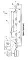
- Figure 1 depicts a basic N-order delta sigma modulator 100.
- the delta sigma modulator 100 includes a difference stage 101 to determine a difference signal u d (n) between an input signal x(n) and a quantizer feedback signal y(n-1).
- the digital input signal x(n) represents an oversampled version of an input signal from a signal source 103, such as a microphone or audio/visual playback device.
- the input signal can be any type of input signal, such as an audio input signal.
- a preprocessor generally includes a digital interpolator to generate the oversampled digital input signal.
- the quantizer feedback signal y(n-1) represents a one (1) cycle delay of the quantizer output signal y(n).
- Delta sigma modulator 100 includes a loop filter 102 to filter the difference signal u d (n).
- the loop filter 102 is implemented using a feed-forward type loop filter topology of order N, wherein N is a positive integer.
- the loop filter 102 includes N series connected filter stages 104.0, 104.1, ... , 104.N-1.
- Each of the filter stages 104.0, 104.1, ... , 104.N-1 includes an integrator, whose z domain representation is depicted in the exploded schematic 106.
- Each integrator of the filter stages 104.0, 104.1, ... , 104.N-1 also generally includes a gain coefficient (not shown) that is determined using well-known digital design techniques to achieve the desired frequency response of the loop filter 102.
- the loop filter 102 functions as a low pass filter during non-quantizer overload conditions with a relatively high gain for frequencies in the baseband.
- the quantizer 108 provides a single-bit or multi-bit output signal y(n).
- the quantizer introduces a quantization error. Filtering of the quantization error by the delta sigma modulator 100 minimizes the quantization error at low, baseband frequencies. Thus, the delta sigma modulator 100 exhibits "noise shaping" behavior by reducing noise in the baseband. Subsequent signal processing of output signal y(n) can filter out signal frequencies, including noise, located above the baseband.
- the attainable signal-to-noise ratio (SNR) of the delta sigma modulator 100 in the baseband depends in part on the amount of oversampling of the original input signal and the order of the loop filter 102. Higher order filters require less oversampling to maintain acceptable SNR. However, the order is limited by instabilities in the loop filter 102. Instabilities in the loop filter 102 can be caused by, for example, large sample-to-sample excursions of the input signal x(n). The order of loop filter 102 is also limited by overload of the quantizer 108. Quantizer overload occurs when the quantizer input signal u f (n) exceeds an input signal peak operating range of the quantizer 108.
- one solution to prevent quantizer overload conservatively limits the amplitude range of the input signal x(n) to values that with a high degree of certainty prevent the delta sigma modulator 100 from going into quantizer overload.
- conservatively limiting the range of input signal x(n) also artificially limits the dynamic range of input signal x(n).
- a second solution for preventing quantizer overload is to clip the quantizer input signal u f (n) and, thus, limit the quantizer input signal u f (n) to values within the non-overload operating range of quantizer 108.
- conventional techniques that limit the quantizer input signal u f (n) suffer from poor signal-to-noise ratios at least during clipping operations.
- U.S. Patent No. 5,243,345 (referred to herein as the "Naus Patent") describes an embodiment of the second quantizer overload prevention solution.
- the Naus Patent describes a delta sigma modulator that includes a feed-forward type loop filter and signal limiters to regressively limit the quantizer input signal u f (n) while providing less restrictions on the amplitude range for the input signal x(n).
- the Naus Patent is entitled "Sigma-Delta Modulator Having a Plural Order Loop Filter with Successive Filter stages of Successively Smaller Signal Excursion Range", inventors Naus et al., filed Feb. 21, 1992, and assigned to U.S. Philips Corp.
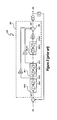
- FIG. 2 depicts one embodiment of the delta sigma modulator 200 described by the Naus Patent.
- the delta sigma modulator 200 includes an N-order, low pass loop filter 202 having series connected filter stages 204.0, 204.1, ... , 204.N-1.
- Each filter stage 204.x includes an integrator 206.x and a limiter 208.x to limit the output signal amplitude of each filter stage 204.x, where x ⁇ ⁇ 0, 1, ... , N-1 ⁇ .
- 204.N-1 are adjusted by respective coefficients c.0, c.1, ..., c.N-1 (also referred to as "weight factors") and added together by an adder stage 208 to generate a filter output/quantizer input signal u f (n).
- G 0 G 1 ...G N-1 represent the gains of respective filter stages 204.0, 204.1, ..., 204.N-1.
- the limiters 210.0, 210.1, ..., 210.N-1 regressively limit the filter stage output signals to respective limit values L 0 , L 1 , ..., L N-1 .
- the limiters prevent instabilities in the delta sigma modulator 200 in the event of an increasing input signal 210.0, 210.1, ..., 210.N-1 by limiting the filter output signal u f (n) with the last limiter 210.N-1 and systematically regressively limiting the output of immediately preceding filter stages.
- the systematic, regressive limitation of preceding filter stages is accomplished by setting limiting values L x in accordance with: L x G 0 ⁇ G 1 ... G x ⁇ L x - 1 G 0 ⁇ G 1 ... G x - 1 , where x ⁇ 0 , 1 , ... , N - 1 .
- the noise performance of the Naus Patent delta sigma modulator suffers during overload conditions because the signal transfer function (STF) of the feed-forward loop filter peaks in the near out of band frequencies, thus, severely compromising low pass performance and accentuating noise during overload.
- STF signal transfer function
- a method of preventing quantizer overload in a delta sigma modulator includes providing quantizer output feedback to an initial filter stage of a loop filter of the delta sigma modulator and providing quantizer feedback to at least one additional filter stage of the loop filter. The method further includes limiting an output of the initial filter stage of the loop filter during quantizer overload prevention conditions and providing an output signal of the initial filter stage to a second filter stage of the loop filter.
- a signal processing system in another embodiment, includes a delta-sigma modulator having a feedback topology to convert an input signal into an output signal.
- the delta-sigma modulator includes a delta sigma modulator input to receive the input signal and a quantizer to quantize a quantizer input signal and provide a quantizer output signal via a quantizer output.
- the delta-sigma modulator further includes a loop filter to provide the quantizer input signal to the quantizer.
- the loop filter includes an initial filter stage having a limiter L 0 to limit an output signal of the initial filter stage.
- the initial filter stage is coupled to the delta sigma modulator input and the quantizer output.
- the loop filter also includes a filter section coupled to an output of the initial filter stage and the quantizer output. A transfer function of the loop filter maintains a low pass transfer function when limiter L 0 is active.
- a signal processing system includes a delta-sigma modulator to convert an input signal into an output signal.
- the delta-sigma modulator includes a quantizer to generate a quantizer output signal and a loop filter coupled to the quantizer.
- the loop filter has a feedback topology.
- the loop filter includes an initial N successive filter stages (FS) arranged in ascending order FS 0 through FS N-1 wherein:
- a method of preventing quantizer overload in a delta sigma modulator includes integrating a first difference signal to produce a first integrated output signal.
- the difference signal includes a difference between a delta sigma modulator input signal and a first quantizer feedback signal.
- the method further includes limiting the first integrated output signal during quantizer overload prevention conditions to produce a first limited output signal.
- the method also includes integrating a second difference signal to produce a second integrated output signal.
- the second difference signal includes a difference between a second quantizer output signal and the first limited output signal, and otherwise the second difference signal includes difference between the second quantizer output signal and the first integrated output signal.
- the method also includes limiting the second integrated output signal if limiting the first integrated output signal is insufficient to prevent quantizer overload.
- an apparatus for preventing quantizer overload in a delta sigma modulator includes means for providing quantizer output feedback to an initial filter stage of a loop filter of the delta sigma modulator.
- the apparatus further includes means for providing quantizer feedback to at least one additional filter stage of the loop filter and means for limiting an output of the initial filter stage of the loop filter during quantizer overload prevention conditions.
- the apparatus also includes means for providing an output signal of the initial filter stage to a second filter stage of the loop filter.
- an apparatus for preventing quantizer overload in a delta sigma modulator includes means for integrating a first difference signal to produce a first integrated output signal, wherein the difference signal comprises a difference between a delta sigma modulator input signal and a first quantizer feedback signal.
- the apparatus also includes means for limiting the first integrated output signal during quantizer overload prevention conditions to produce a first limited output signal.
- the apparatus further includes means for integrating a second difference signal to produce a second integrated output signal, wherein, during quantizer overload prevention conditions, the second difference signal comprises a difference between a second quantizer output signal and the first limited output signal, and otherwise the second difference signal comprises a difference between the second quantizer output signal and the first integrated output signal.
- the apparatus also includes means for limiting the second integrated output signal if limiting the first integrated output signal is insufficient to prevent quantizer overload.
- Figure 1 (labeled prior art) depicts an N-order delta sigma modulator.
- Figure 2 (labeled prior art) depicts a feed-forward-type N-order delta sigma modulator with systematic, regressive limitation of filter stages beginning with the (N-1) filter stage.
- Figure 3 depicts a quantizer overload protected, feedback-type delta sigma modulator with progressive limitation of filter stages.
- Figure 4 depicts a quantizer overload protected, feedback-type delta sigma modulator with progressive limitation of filter stages and forward path delays in one or more filter stages.
- Figure 5 depicts an exemplary signal processing system that includes a quantizer overload protected, feedback-type delta sigma modulator.
- a digital signal processing system includes a delta sigma modulator with a loop filter that maintains a low pass output and a relatively high signal-to-noise ratio during quantizer overload prevention conditions.
- the low pass output is achieved by maintaining a low pass transfer function of a closed loop in the delta sigma modulator during quantizer overload prevention conditions.
- the closed loop includes a filter section of the loop filter coupled to a quantizer of the delta sigma modulator.
- quantizer overload prevention conditions refer to predetermined output signal levels of at least the initial filter stage of the delta sigma modulator loop filter that could cause the quantizer to overload.
- the delta sigma modulator includes a quantizer overload protected delta sigma modulator with an N-order feedback-type loop filter that initially limits an output of an initial filter stage during quantizer overload prevention conditions. In at least one embodiment, if limiting the output of the initial filter stage is insufficient to prevent quantizer overload, the delta sigma modulator progressively limits an output of at least the next successive filter stage to prevent quantizer overload, where N is a positive integer greater than or equal to two (2).
- a quantizer of the delta sigma modulator provides feedback to at least the first two filter stages of the loop filter.
- the N filter stages are successively coupled to each other so that each of the N-1 filter stages after the initial filter stage receives an output signal from the immediately preceding filter stage.
- the delta sigma modulator utilizes a feedback loop filter topology
- the signal transfer function of the delta sigma modulator is low pass.
- the signal processed by the loop filter is filtered at a high rate before being clipped, which helps reduce clipping artifacts that would otherwise degrade the SNR of the delta sigma modulator output signal.
- limiters limit the output of one or more of the subsequent filter stages.
- the limiter of the initial filter stage is configured to limit the output of the initial filter stage before any subsequent limiter limits the output of any subsequent filter stage.
- the limiters are configured to progressively limit successive filter stages.
- the filter stages include a first order integrator, and the limiter for each filter stage resides within a loop of the integrator.
- each limiter not only limits the output of a filter stage, the limiter also provides a limit for the state variable(s) of each integrator.
- a delay is included in a forward path of at least the initial filter stage and preferably in the forward path of each filter stage of the loop filter to improve the SNR of the delta sigma modulator.
- the feedback-type delta sigma modulator exhibits superior noise reduction, stability, and faster recovery from quantizer overload than conventional technologies such as the feed-forward with limiters technology disclosed in the Naus Patent.
- the noise performance of the Naus Patent delta sigma modulator suffers during overload prevention conditions because the signal transfer function (STF) of the feed-forward loop filter peaks in the near out of band frequencies, thus, potentially severely compromising low pass performance and accentuating noise during overload.
- STF signal transfer function
- embodiments of the feedback-type delta sigma modulator with overload prevention described herein maintain a low pass loop filter transfer function with a sharp cut-off frequency in the near out of band frequencies.
- the feedback-type delta sigma modulator maintains superior noise reduction performance.
- the Naus Patent discloses limiting the output of each filter stage with a limiter connected outside of the integrating network.
- increasing signals to the filter stage continue to cause the state variable(s) of the integrating network to increase.
- recovery time from input signals in an overload range increases and SNR can decrease during the extended recovery time.
- FIG. 3 depicts one embodiment of a quantizer overload protected, feedback-type delta sigma modulator.
- the delta sigma modulator 300 utilizes a feedback-type loop filter 302 with at least two successive filter stages.
- the delta sigma modulator 300 receives an oversampled input signal x(n), low pass filters input signal x(n), quantizes the filtered signal u f (n), and generates a quantizer output signal y(n).
- the loop filter includes N successive filter stages (FS) FS 0 , FS 1 , ...., FS N-1, and at least the initial filter stage, FS 0, includes limiter 306.0 to limit the respective filter stage output signal uo 0 during quantizer overload prevention conditions, where N ⁇ 2.
- Filter stages FS 1 through FS N-1 and the quantizer 302 form a closed loop 307 through the feedback path that includes delay 304.
- the output signal uo 0 of the initial filter stage FS 0 can include harmonics outside the baseband frequencies.
- the closed loop 307 maintains a low pass transfer function and, thus, attenuates the harmonics, when the limiter 306.0 is active during overload prevention conditions.
- one or more successive filter stages FS 1 ,..., FS N-1 also include limiters 306.1, ..., 306.N-1 (shown in dashed lines) to limit the respective output signals of filter stages FS 1 , FS 2 , ..., FS N-1 during quantizer overload prevention conditions.
- closed loop 307 maintains a low pass transfer function when any of limiters 306.0, 306.1, ..., 306.N-1 are active.
- each limiter 306.1 included in loop filter 302 is inactive, i.e. the limiter 306.i does not limit the input signal ui i .
- Filter stage FS 0 is the initial filter stage, and when a potential quantizer overload prevention condition is detected the limiter L 0 of filter stage FS 0 is active to limit the output signal uo 0 before any subsequent limiter in subsequent filter stages becomes active, i.e. the input signal to the limiter reaches a predetermined level and begins limiting the output signal of the respective filter stage.
- the limit levels L (also commonly referred to as "clipping levels") of each filter stage having a limiter are preferably set to prevent quantizer overload. Comparator technology can be used to determine when an input signal ui i to a limiter has reached the limit L i of the limiter 306 i . If the input signal ui i reaches the limit L i , the limiter 306.i is activated and limits (clips) the input signal ui i to limit L i . In one embodiment, the limit L i represents a magnitude level that in most cases will prevent quantizer overload.
- the initial limiter 306.0 limits the input signal ui 0 to 1dB to 3dB above the signal level seen at filter stage FS 0 for a normal full scale value of input signal ui 0 .
- the limits L i for optional limiters 306.1 through 306.N-1 in filter stages after the initial filter stage are set to approximately 6 dB above a normal full-scale design input signal ui i , i ⁇ ⁇ 1, 2, ..., N-1 ⁇ .
- the quantizer can be designed to generate a single-bit or multi-bit quantizer output signal y(n).
- the quantizer output signal y(n) is fed back through a delay 304 to each of the N successive filter stages FS 0 , FS 1 ,..., FS N-1 .
- the delayed quantizer output signal y(n-1) can be weighted by coefficients c 0 , c 1 , ... , C N-1 to obtain a desired frequency response.
- Determination of the coefficients c 0 , c 1 ,..., c N-1 can be accomplished conventionally as, for example, described in Norsworthy et al, "Delta Sigma Data Converters - Theory, Design, and Simulation", 1997, ISBN 0-7803-1045-4, particularly in chapters 3 and 5.
- Loop filter 302 is depicted with at least four (4) filter stages, an initial filter stage FS 0 and a filter section that includes at least three (3) subsequent filter stages FS 1 , FS 2 , and FS N-1.
- the number N of filter stages is a design choice and is any number greater than or equal to two (2).
- the loop filter 302 can also include additional filter stages coupled to the N initial filter stages.
- the additional filter stages are also not required to include limiters.
- each filter stage FS i is a first order integrator with a limiter 306 i in the integration loop. Inclusion of the limiter 306 i in the integration loop limits the output of filter stage FS i to prevent quantizer overload and limits the state variable of filter stage FS i to a maximum value to speed recovery from overload prevention conditions.
- the initial filter stage FS 0 receives an input signal ui 0 (n) derived from the delta sigma modulator input signal x(n) and the quantizer feedback signal y(n).
- the first stage input signal ui 0 (n) is a difference between input signal x(n) and the weighted quantizer output signal c 0 ⁇ y(n-1), i.e. ui 0 ⁇ (n)-[c 0 ⁇ y(n-1)].
- the input signal ui i (n) for each subsequent filter stage FS i , i ⁇ ⁇ 1, 2, ..., N -1 ⁇ is derived from the output signal uo i-1 (n) of the previous filter stage FS i-1 and the quantizer feedback signal y(n).
- the input signal ui i (n) uo i-1 (n) -[c i ⁇ y(n-1)].
- "(n)" is omitted from the filter stage input and output signals to limit congestion.
- limiter 306 i limits the output signal uo i of filter stage FS i to a predetermined level limit L i if the input signal ui i (n)+uo i (n-1) reaches limit L i .
- Signs of values can be manipulated to change addition operations to subtraction operations and visa versa.
- the predetermined limit L 0 is established so that limiter 306.0 will limit the output signal uo 0 of filter stage FS 0 before any subsequent limiters 306.1-306.N-1 limit the respective output signals of filter stages FS 1 through FS N-1 .
- the predetermined limit L 0 is set so that limiting by limiter 306.0 does not occur until the input signal x(n) is 10-20% above a full-scale value of filter stage when the delta sigma modulator 300 is excited by input signal ui 0 (n).
- the full-scale value of filter stage input signal ui 0 (n) is defined by the modulation index of delta sigma modulator 300 times the quantizer feedback signal y(n).
- limiters 306.0 through 306.N-1 progressively limit respective filter stages FS 0 through FS N-1 to maximize noise reduction and minimize recovery time.
- loop filter 302 can also include an optional resonator 308 with a gain coefficient of-gl.
- Resonators are commonly used in delta sigma modulator loop filters to provide more effective noise shaping.
- Figure 4 depicts another embodiment of a quantizer overload protected, feedback-type delta sigma modulator.
- the delta sigma modulator 400 is identical to delta sigma modulator 300 except that delays 402.0, 402.1, ..., 402.N-1 are included in the respective forward paths of the filter stages FS 0 , FS 1 , ..., FS N-1 rather than in the feedback loop of the filter stage integrators.
- the delays 402.0, 402.1, ..., 402.N-1 improve the low pass filter characteristics of the loop filter 400 of delta sigma modulator 400 during quantizer overload prevention conditions.
- the transfer function of each filter stage FS 0 , FS 1 , ..., FS N-1 with forward path delays is (z -1 )/(1- z -1 ).
- one or more of filter stages FS 0 , FS 1 , ..., FS N-1 limits the respective filter stage output signal, and delta sigma modulator 400 continues to modulate the delta sigma modulator input signal x(n) with a low pass filter transfer function.
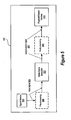
- signal processing system 500 depicts one embodiment of a signal processing system that includes a delta sigma modulator 502 that maintains a low pass loop filter transfer function during quantizer overload prevention conditions.
- the delta sigma modulator 502 represents delta sigma modulators such as delta sigma modulator 300 and delta sigma modulator 400, which both include a loop filter for progressively limiting filter stage output signals to provide quantizer overload prevention.
- Signal processing system 500 is particularly useful for use in a digital-to-analog (“DAC") implementation to drive output devices such as audio speakers.
- DAC digital-to-analog
- Signal processing system 500 processes an input signal 504 generated by an input signal source 503.
- the input signal 504 may be digital or analog and may be from any signal source including signals generated as part of a recording/mixing process or other high end audio sources or from lower-end sources such as a compact disk player, MP3 player, audio/video system, audio tape player, or other signal recording and/or playback device.
- the input signal 504 may be an audio signal, a video signal, an audio plus video signal, and/or other signal type.
- input signal 504 undergoes some preprocessing 506 prior to being modulated by delta sigma modulator 502.
- pre-processing 506 can involve an interpolation filter to oversample a digital input signal 504 in a well-known manner.
- Pre-processing 506 can include an analog-to-digital converter to convert an analog input signal 504 into a digital signal.
- Pre-processing 506 can also include mixing, reverberation, equalization, editing, out-of-band noise filtering and other filtering operations.
- pre-processing 506 provides discrete input signals x[n] to look-ahead delta sigma modulator 502.
- Each discrete input signal x[n] is an N-bit signal, where N is greater than one.
- look-ahead delta sigma modulator 502 processes M input signals x[n] and patterns of M output candidates y[n] to determine an output signal 507 from the output candidates corresponding to each input signal x[n].
- Output signal 507 is, for example, a collection of one-bit output values. The output signal 507, thus, becomes an encoded version of the input signal 504.
- Signal processing system 500 typically includes post-processing 508 to post-process the output signal 507 of delta sigma modulator 502.
- Post-processing 508 can include an analog filter to convert the output signal 507 into an analog drive signal for playback/output devices 510.
- the playback/output devices 510 represent audio speakers.
- the signal processing systems disclosed herein can be manufactured using well-known integrated, discrete, or a combination of integrated and discrete components. Additionally, software in combination with a processor can be used to implement features of the signal processing systems. In particular, the delta sigma modulators described herein can be implemented using hardware, software, or a combination of hardware and software.
Landscapes
- Engineering & Computer Science (AREA)
- Theoretical Computer Science (AREA)
- Compression, Expansion, Code Conversion, And Decoders (AREA)
Abstract
Description
- The present invention relates in general to the field of signal processing, and more specifically to a system and method for providing overload prevention for delta-sigma modulators using a multi-order, feedback loop filter topology.
- Delta sigma modulators produce a high resolution output signal using a low-resolution quantizer. Delta sigma modulators achieve the high resolution by using oversampling data rates higher than the Nyquist rate. Many signal processing systems include delta sigma modulators to quantize an input signal into one or more bits at a high rate to produce a high resolution output signal. "Delta-sigma modulators" are also commonly referred to using other interchangeable terms such as "sigma-delta modulators", "delta-sigma converters", "sigma delta converters", and "noise shapers".
-
Figure 1 depicts a basic N-orderdelta sigma modulator 100. Thedelta sigma modulator 100 includes adifference stage 101 to determine a difference signal ud(n) between an input signal x(n) and a quantizer feedback signal y(n-1). The digital input signal x(n) represents an oversampled version of an input signal from asignal source 103, such as a microphone or audio/visual playback device. The input signal can be any type of input signal, such as an audio input signal. A preprocessor generally includes a digital interpolator to generate the oversampled digital input signal. The quantizer feedback signal y(n-1) represents a one (1) cycle delay of the quantizer output signal y(n). Deltasigma modulator 100 includes aloop filter 102 to filter the difference signal ud(n). Theloop filter 102 is implemented using a feed-forward type loop filter topology of order N, wherein N is a positive integer. Theloop filter 102 includes N series connected filter stages 104.0, 104.1, ... , 104.N-1. Each of the filter stages 104.0, 104.1, ... , 104.N-1 includes an integrator, whose z domain representation is depicted in the exploded schematic 106. The output signals of all filter stages 104.0, 104.1, ... , 104.N-1 are adjusted by respective coefficients c0, c1, ..., CN-1 (also referred to as "weight factors") and added together by an adder stage 110 to generate a filter output/quantizer input signal uf(n). Each integrator of the filter stages 104.0, 104.1, ... , 104.N-1 also generally includes a gain coefficient (not shown) that is determined using well-known digital design techniques to achieve the desired frequency response of theloop filter 102. For low frequency baseband signals, such as audio signals (approx. 0 Hz to 25 kHz), theloop filter 102 functions as a low pass filter during non-quantizer overload conditions with a relatively high gain for frequencies in the baseband. - The
quantizer 108 provides a single-bit or multi-bit output signal y(n). The quantizer introduces a quantization error. Filtering of the quantization error by thedelta sigma modulator 100 minimizes the quantization error at low, baseband frequencies. Thus, thedelta sigma modulator 100 exhibits "noise shaping" behavior by reducing noise in the baseband. Subsequent signal processing of output signal y(n) can filter out signal frequencies, including noise, located above the baseband. - The attainable signal-to-noise ratio (SNR) of the
delta sigma modulator 100 in the baseband depends in part on the amount of oversampling of the original input signal and the order of theloop filter 102. Higher order filters require less oversampling to maintain acceptable SNR. However, the order is limited by instabilities in theloop filter 102. Instabilities in theloop filter 102 can be caused by, for example, large sample-to-sample excursions of the input signal x(n). The order ofloop filter 102 is also limited by overload of thequantizer 108. Quantizer overload occurs when the quantizer input signal uf(n) exceeds an input signal peak operating range of thequantizer 108. In multi-order delta sigma modulators, estimating a maximum range of input signal x(n) that will with certainty prevent the quantizer input signal ud(n) from a obtaining a value outside the operation range ofquantizer 108 is difficult to determine exactly. Estimations of a maximum range for input signal x(n) remains difficult because of the complexity of causal relationships, the influence of noise generated by the delta sigma modulator from non-ideal physical components, rounding errors, and/or other factors. - Consequently, one solution to prevent quantizer overload conservatively limits the amplitude range of the input signal x(n) to values that with a high degree of certainty prevent the
delta sigma modulator 100 from going into quantizer overload. However, conservatively limiting the range of input signal x(n) also artificially limits the dynamic range of input signal x(n). A second solution for preventing quantizer overload is to clip the quantizer input signal uf(n) and, thus, limit the quantizer input signal uf(n) to values within the non-overload operating range ofquantizer 108. However, conventional techniques that limit the quantizer input signal uf(n) suffer from poor signal-to-noise ratios at least during clipping operations. -
U.S. Patent No. 5,243,345 (referred to herein as the "Naus Patent") describes an embodiment of the second quantizer overload prevention solution. The Naus Patent describes a delta sigma modulator that includes a feed-forward type loop filter and signal limiters to regressively limit the quantizer input signal uf(n) while providing less restrictions on the amplitude range for the input signal x(n). The Naus Patent is entitled "Sigma-Delta Modulator Having a Plural Order Loop Filter with Successive Filter stages of Successively Smaller Signal Excursion Range", inventors Naus et al., filed Feb. 21, 1992, and assigned to U.S. Philips Corp. -
Figure 2 depicts one embodiment of thedelta sigma modulator 200 described by the Naus Patent. Thedelta sigma modulator 200 includes an N-order, lowpass loop filter 202 having series connected filter stages 204.0, 204.1, ... , 204.N-1. Each filter stage 204.x includes an integrator 206.x and a limiter 208.x to limit the output signal amplitude of each filter stage 204.x, where x ∈ {0, 1, ... , N-1}. The output signals of all filter stages 204.0, 204.1, ... , 204.N-1 are adjusted by respective coefficients c.0, c.1, ..., c.N-1 (also referred to as "weight factors") and added together by anadder stage 208 to generate a filter output/quantizer input signal uf(n). Theloop filter 202 functions in accordance with the transfer function:
- where G0G1...GN-1 represent the gains of respective filter stages 204.0, 204.1, ..., 204.N-1. The limiters 210.0, 210.1, ..., 210.N-1 regressively limit the filter stage output signals to respective limit values L0, L1, ..., LN-1.
- The limiters prevent instabilities in the
delta sigma modulator 200 in the event of an increasing input signal 210.0, 210.1, ..., 210.N-1 by limiting the filter output signal uf(n) with the last limiter 210.N-1 and systematically regressively limiting the output of immediately preceding filter stages. The systematic, regressive limitation of preceding filter stages is accomplished by setting limiting values Lx in accordance with:
- However, the noise performance of the Naus Patent delta sigma modulator suffers during overload conditions because the signal transfer function (STF) of the feed-forward loop filter peaks in the near out of band frequencies, thus, severely compromising low pass performance and accentuating noise during overload.
- Researchers continue to seek solutions to prevent quantizer overload, achieve faster quantizer overload recovery times, and maintain acceptable signal-to-noise ratios.
- In one embodiment of the present invention, a method of preventing quantizer overload in a delta sigma modulator includes providing quantizer output feedback to an initial filter stage of a loop filter of the delta sigma modulator and providing quantizer feedback to at least one additional filter stage of the loop filter. The method further includes limiting an output of the initial filter stage of the loop filter during quantizer overload prevention conditions and providing an output signal of the initial filter stage to a second filter stage of the loop filter.
- In another embodiment of the present invention, a signal processing system includes a delta-sigma modulator having a feedback topology to convert an input signal into an output signal. The delta-sigma modulator includes a delta sigma modulator input to receive the input signal and a quantizer to quantize a quantizer input signal and provide a quantizer output signal via a quantizer output. The delta-sigma modulator further includes a loop filter to provide the quantizer input signal to the quantizer. The loop filter includes an initial filter stage having a limiter L0 to limit an output signal of the initial filter stage. The initial filter stage is coupled to the delta sigma modulator input and the quantizer output. The loop filter also includes a filter section coupled to an output of the initial filter stage and the quantizer output. A transfer function of the loop filter maintains a low pass transfer function when limiter L0 is active.
- In a further embodiment of the present invention, a signal processing system includes a delta-sigma modulator to convert an input signal into an output signal. The delta-sigma modulator includes a quantizer to generate a quantizer output signal and a loop filter coupled to the quantizer. The loop filter has a feedback topology. The loop filter includes an initial N successive filter stages (FS) arranged in ascending order FS0 through FSN-1 wherein:
- filter stage FS0 receives a difference signal comprised of a difference between the input signal and the quantizer output signal;
- each of the initial N successive filter stages FS0 through FSN-1 receives input signals comprised of a feedback signal from the quantizer and an input signal from a preceding filter stage;
- each of the filter stages includes an integrator;
- filter stage FS0 includes limiter L0 to limit output values of filter stage FS0 to a maximum absolute value;
- N is a non-negative integers and N ≥ 2.
- In another embodiment of the present invention, a method of preventing quantizer overload in a delta sigma modulator includes integrating a first difference signal to produce a first integrated output signal. The difference signal includes a difference between a delta sigma modulator input signal and a first quantizer feedback signal. The method further includes limiting the first integrated output signal during quantizer overload prevention conditions to produce a first limited output signal. The method also includes integrating a second difference signal to produce a second integrated output signal. During quantizer overload prevention conditions, the second difference signal includes a difference between a second quantizer output signal and the first limited output signal, and otherwise the second difference signal includes difference between the second quantizer output signal and the first integrated output signal. The method also includes limiting the second integrated output signal if limiting the first integrated output signal is insufficient to prevent quantizer overload.
- In another embodiment of the present invention, an apparatus for preventing quantizer overload in a delta sigma modulator includes means for providing quantizer output feedback to an initial filter stage of a loop filter of the delta sigma modulator. The apparatus further includes means for providing quantizer feedback to at least one additional filter stage of the loop filter and means for limiting an output of the initial filter stage of the loop filter during quantizer overload prevention conditions. The apparatus also includes means for providing an output signal of the initial filter stage to a second filter stage of the loop filter.
- In a further embodiment of the present invention, an apparatus for preventing quantizer overload in a delta sigma modulator includes means for integrating a first difference signal to produce a first integrated output signal, wherein the difference signal comprises a difference between a delta sigma modulator input signal and a first quantizer feedback signal. The apparatus also includes means for limiting the first integrated output signal during quantizer overload prevention conditions to produce a first limited output signal. The apparatus further includes means for integrating a second difference signal to produce a second integrated output signal, wherein, during quantizer overload prevention conditions, the second difference signal comprises a difference between a second quantizer output signal and the first limited output signal, and otherwise the second difference signal comprises a difference between the second quantizer output signal and the first integrated output signal. The apparatus also includes means for limiting the second integrated output signal if limiting the first integrated output signal is insufficient to prevent quantizer overload.
- The present invention may be better understood, and its numerous objects, features and advantages made apparent to those skilled in the art by referencing the accompanying drawings. The use of the same reference number throughout the several figures designates a like or similar element.
-
Figure 1 (labeled prior art) depicts an N-order delta sigma modulator. -
Figure 2 (labeled prior art) depicts a feed-forward-type N-order delta sigma modulator with systematic, regressive limitation of filter stages beginning with the (N-1) filter stage. -
Figure 3 depicts a quantizer overload protected, feedback-type delta sigma modulator with progressive limitation of filter stages. -
Figure 4 depicts a quantizer overload protected, feedback-type delta sigma modulator with progressive limitation of filter stages and forward path delays in one or more filter stages. -
Figure 5 depicts an exemplary signal processing system that includes a quantizer overload protected, feedback-type delta sigma modulator. - A digital signal processing system includes a delta sigma modulator with a loop filter that maintains a low pass output and a relatively high signal-to-noise ratio during quantizer overload prevention conditions. The low pass output is achieved by maintaining a low pass transfer function of a closed loop in the delta sigma modulator during quantizer overload prevention conditions. The closed loop includes a filter section of the loop filter coupled to a quantizer of the delta sigma modulator. In at least one embodiment, quantizer overload prevention conditions refer to predetermined output signal levels of at least the initial filter stage of the delta sigma modulator loop filter that could cause the quantizer to overload. In at least one embodiment, the delta sigma modulator includes a quantizer overload protected delta sigma modulator with an N-order feedback-type loop filter that initially limits an output of an initial filter stage during quantizer overload prevention conditions. In at least one embodiment, if limiting the output of the initial filter stage is insufficient to prevent quantizer overload, the delta sigma modulator progressively limits an output of at least the next successive filter stage to prevent quantizer overload, where N is a positive integer greater than or equal to two (2). A quantizer of the delta sigma modulator provides feedback to at least the first two filter stages of the loop filter.
- The initial filter stage, N=0, of the loop filter receives an input signal derived from an input signal to the delta sigma modulator ("DSM input signal") and a negative feedback signal derived from a quantizer output signal. The N filter stages are successively coupled to each other so that each of the N-1 filter stages after the initial filter stage receives an output signal from the immediately preceding filter stage. The second filter stage, N=1, also receives a negative feedback signal derived from the quantizer output signal. In at least one embodiment, one or more subsequent filter stages, N={2, 3, ..., and/or N-1 }, also receive a negative feedback signal derived from the quantizer output signal. Because the delta sigma modulator utilizes a feedback loop filter topology, the signal transfer function of the delta sigma modulator is low pass. Thus, the signal processed by the loop filter is filtered at a high rate before being clipped, which helps reduce clipping artifacts that would otherwise degrade the SNR of the delta sigma modulator output signal.
- For the initial filter stage, N=0, and in one embodiment for one or more filter stages subsequent to the initial filter stage, limiters limit the output of one or more of the subsequent filter stages. The limiter of the initial filter stage is configured to limit the output of the initial filter stage before any subsequent limiter limits the output of any subsequent filter stage. In at least one embodiment, the limiters are configured to progressively limit successive filter stages. In at least one embodiment, the filter stages include a first order integrator, and the limiter for each filter stage resides within a loop of the integrator. Thus, each limiter not only limits the output of a filter stage, the limiter also provides a limit for the state variable(s) of each integrator. In at least one embodiment, a delay is included in a forward path of at least the initial filter stage and preferably in the forward path of each filter stage of the loop filter to improve the SNR of the delta sigma modulator.
- In simulation, the feedback-type delta sigma modulator exhibits superior noise reduction, stability, and faster recovery from quantizer overload than conventional technologies such as the feed-forward with limiters technology disclosed in the Naus Patent. As noted previously, the noise performance of the Naus Patent delta sigma modulator suffers during overload prevention conditions because the signal transfer function (STF) of the feed-forward loop filter peaks in the near out of band frequencies, thus, potentially severely compromising low pass performance and accentuating noise during overload. In contrast, embodiments of the feedback-type delta sigma modulator with overload prevention described herein maintain a low pass loop filter transfer function with a sharp cut-off frequency in the near out of band frequencies. Thus, during overload prevention, the feedback-type delta sigma modulator maintains superior noise reduction performance. Additionally, the Naus Patent discloses limiting the output of each filter stage with a limiter connected outside of the integrating network. However, increasing signals to the filter stage continue to cause the state variable(s) of the integrating network to increase. Thus, recovery time from input signals in an overload range increases and SNR can decrease during the extended recovery time.
-
Figure 3 depicts one embodiment of a quantizer overload protected, feedback-type delta sigma modulator. Thedelta sigma modulator 300 utilizes a feedback-type loop filter 302 with at least two successive filter stages. Thedelta sigma modulator 300 receives an oversampled input signal x(n), low pass filters input signal x(n), quantizes the filtered signal uf(n), and generates a quantizer output signal y(n). The loop filter includes N successive filter stages (FS) FS0, FS1, ...., FSN-1, and at least the initial filter stage, FS0, includes limiter 306.0 to limit the respective filter stage output signal uo0 during quantizer overload prevention conditions, where N ≥ 2. Filter stages FS1 through FSN-1 and thequantizer 302 form aclosed loop 307 through the feedback path that includesdelay 304. When the limiter 306.0 is active during overload prevention conditions, the output signal uo0 of the initial filter stage FS0 can include harmonics outside the baseband frequencies. In at least one embodiment, theclosed loop 307 maintains a low pass transfer function and, thus, attenuates the harmonics, when the limiter 306.0 is active during overload prevention conditions. Optionally, one or more successive filter stages FS1,..., FSN-1 also include limiters 306.1, ..., 306.N-1 (shown in dashed lines) to limit the respective output signals of filter stages FS1, FS2, ..., FSN-1 during quantizer overload prevention conditions. In at least one embodiment, closedloop 307 maintains a low pass transfer function when any of limiters 306.0, 306.1, ..., 306.N-1 are active. - During non-overload prevention conditions, each limiter 306.1 included in
loop filter 302 is inactive, i.e. the limiter 306.i does not limit the input signal uii. Filter stage FS0 is the initial filter stage, and when a potential quantizer overload prevention condition is detected the limiter L0 of filter stage FS0 is active to limit the output signal uo0 before any subsequent limiter in subsequent filter stages becomes active, i.e. the input signal to the limiter reaches a predetermined level and begins limiting the output signal of the respective filter stage. - The limit levels L (also commonly referred to as "clipping levels") of each filter stage having a limiter are preferably set to prevent quantizer overload. Comparator technology can be used to determine when an input signal uii to a limiter has reached the limit Li of the limiter 306i. If the input signal uii reaches the limit Li, the limiter 306.i is activated and limits (clips) the input signal uii to limit Li. In one embodiment, the limit Li represents a magnitude level that in most cases will prevent quantizer overload. Generally, the initial limiter 306.0 limits the input signal ui0 to 1dB to 3dB above the signal level seen at filter stage FS0 for a normal full scale value of input signal ui0. In one embodiment, the limits Li for optional limiters 306.1 through 306.N-1 in filter stages after the initial filter stage are set to approximately 6 dB above a normal full-scale design input signal uii, i ∈ { 1, 2, ..., N-1}.
- Simulation has indicated that using a 5th order (i.e. N=5) feedback-type delta sigma modulator 300 with progressive filter stage output signal limitation can reduce noise in the delta sigma modulator output signal y(n) by 40dB in response to a sine wave input signal x(n) that exceeds 3 dB past normal full-scale. Normal full-scale for input signal x(n) is generally set so as to reduce the likelihood of quantizer overload and other signal distortion. An "acceptable likelihood" of quantizer overload and other signal distortion is a matter of design choice.
- The quantizer can be designed to generate a single-bit or multi-bit quantizer output signal y(n). The quantizer output signal y(n) is fed back through a
delay 304 to each of the N successive filter stages FS0, FS1,..., FSN-1. The delayed quantizer output signal y(n-1) can be weighted by coefficients c0, c1, ... , CN-1 to obtain a desired frequency response. Determination of the coefficients c0, c1,..., cN-1 can be accomplished conventionally as, for example, described in Norsworthy et al, "Delta Sigma Data Converters - Theory, Design, and Simulation", 1997, ISBN 0-7803-1045-4, particularly inchapters 3 and 5. -
Loop filter 302 is depicted with at least four (4) filter stages, an initial filter stage FS0 and a filter section that includes at least three (3) subsequent filter stages FS1, FS2, and FSN-1. In other embodiments, the number N of filter stages is a design choice and is any number greater than or equal to two (2). Theloop filter 302 can also include additional filter stages coupled to the N initial filter stages. The additional filter stages are also not required to include limiters. In at least one embodiment, each filter stage FSi is a first order integrator with a limiter 306i in the integration loop. Inclusion of the limiter 306i in the integration loop limits the output of filter stage FSi to prevent quantizer overload and limits the state variable of filter stage FSi to a maximum value to speed recovery from overload prevention conditions. - During operation of
delta sigma modulator 300, the initial filter stage FS0 receives an input signal ui0(n) derived from the delta sigma modulator input signal x(n) and the quantizer feedback signal y(n). In one embodiment, the first stage input signal ui0(n) is a difference between input signal x(n) and the weighted quantizer output signal c0 × y(n-1), i.e. ui0 ×(n)-[c0 × y(n-1)]. The input signal uii(n) for each subsequent filter stage FSi, i ∈ {1, 2, ..., N -1}, is derived from the output signal uoi-1(n) of the previous filter stage FSi-1 and the quantizer feedback signal y(n). In one embodiment for i ∈ {1, 2, ..., N -1}, the input signal uii(n) = uoi-1(n) -[ci × y(n-1)]. In the figures, "(n)" is omitted from the filter stage input and output signals to limit congestion. - For i ∈ {1, 2,..., N-1} , limiter 306i limits the output signal uoi of filter stage FSi to a predetermined level limit Li if the input signal uii(n)+uoi(n-1) reaches limit Li. Signs of values can be manipulated to change addition operations to subtraction operations and visa versa.
- The predetermined limit L0 is established so that limiter 306.0 will limit the output signal uo0 of filter stage FS0 before any subsequent limiters 306.1-306.N-1 limit the respective output signals of filter stages FS1 through FSN-1. In one embodiment, the predetermined limit L0 is set so that limiting by limiter 306.0 does not occur until the input signal x(n) is 10-20% above a full-scale value of filter stage when the
delta sigma modulator 300 is excited by input signal ui0(n). In at least one embodiment, the full-scale value of filter stage input signal ui0(n) is defined by the modulation index ofdelta sigma modulator 300 times the quantizer feedback signal y(n). Preferably limiters 306.0 through 306.N-1 progressively limit respective filter stages FS0 through FSN-1 to maximize noise reduction and minimize recovery time. - Conventional filter design techniques can be utilized in conjunction with the progressive filter stage output signal limitation. For example,
loop filter 302 can also include anoptional resonator 308 with a gain coefficient of-gl. Resonators are commonly used in delta sigma modulator loop filters to provide more effective noise shaping. -
Figure 4 depicts another embodiment of a quantizer overload protected, feedback-type delta sigma modulator. Thedelta sigma modulator 400 is identical to delta sigma modulator 300 except that delays 402.0, 402.1, ..., 402.N-1 are included in the respective forward paths of the filter stages FS0, FS1, ..., FSN-1 rather than in the feedback loop of the filter stage integrators. The delays 402.0, 402.1, ..., 402.N-1 improve the low pass filter characteristics of theloop filter 400 of delta sigma modulator 400 during quantizer overload prevention conditions. In one embodiment, the transfer function of each filter stage FS0, FS1, ..., FSN-1 with forward path delays is (z-1)/(1- z-1). Therefore, during quantizer overload prevention conditions, one or more of filter stages FS0, FS1, ..., FSN-1 limits the respective filter stage output signal, anddelta sigma modulator 400 continues to modulate the delta sigma modulator input signal x(n) with a low pass filter transfer function. - Referring to
Figure 5 ,signal processing system 500 depicts one embodiment of a signal processing system that includes a delta sigma modulator 502 that maintains a low pass loop filter transfer function during quantizer overload prevention conditions. Thedelta sigma modulator 502 represents delta sigma modulators such asdelta sigma modulator 300 anddelta sigma modulator 400, which both include a loop filter for progressively limiting filter stage output signals to provide quantizer overload prevention.Signal processing system 500 is particularly useful for use in a digital-to-analog ("DAC") implementation to drive output devices such as audio speakers.Signal processing system 500 processes aninput signal 504 generated by aninput signal source 503. Theinput signal 504 may be digital or analog and may be from any signal source including signals generated as part of a recording/mixing process or other high end audio sources or from lower-end sources such as a compact disk player, MP3 player, audio/video system, audio tape player, or other signal recording and/or playback device. - The
input signal 504 may be an audio signal, a video signal, an audio plus video signal, and/or other signal type. Generally,input signal 504 undergoes somepreprocessing 506 prior to being modulated bydelta sigma modulator 502. For example, pre-processing 506 can involve an interpolation filter to oversample adigital input signal 504 in a well-known manner. Pre-processing 506 can include an analog-to-digital converter to convert ananalog input signal 504 into a digital signal. Pre-processing 506 can also include mixing, reverberation, equalization, editing, out-of-band noise filtering and other filtering operations. - In the digital domain, pre-processing 506 provides discrete input signals x[n] to look-ahead
delta sigma modulator 502. Each discrete input signal x[n] is an N-bit signal, where N is greater than one. As previously described in more detail, look-ahead delta sigma modulator 502 processes M input signals x[n] and patterns of M output candidates y[n] to determine anoutput signal 507 from the output candidates corresponding to each input signal x[n].Output signal 507 is, for example, a collection of one-bit output values. Theoutput signal 507, thus, becomes an encoded version of theinput signal 504. -
Signal processing system 500 typically includes post-processing 508 to post-process theoutput signal 507 ofdelta sigma modulator 502. Post-processing 508 can include an analog filter to convert theoutput signal 507 into an analog drive signal for playback/output devices 510. In at least one embodiment, the playback/output devices 510 represent audio speakers. - The signal processing systems disclosed herein can be manufactured using well-known integrated, discrete, or a combination of integrated and discrete components. Additionally, software in combination with a processor can be used to implement features of the signal processing systems. In particular, the delta sigma modulators described herein can be implemented using hardware, software, or a combination of hardware and software.
- Although the present invention has been described in detail, it should be understood that various changes, substitutions and alterations can be made hereto without departing from the spirit and scope of the invention as defined by the appended claims.
Embodiments of the invention may also relate to one or more of the following examples: - 1. A method of preventing quantizer overload in a delta sigma modulator, the method comprising:
- providing quantizer output feedback to an initial filter stage of a loop filter of the delta sigma modulator;
- providing quantizer feedback to at least one additional filter stage of the loop filter;
- limiting an output of the initial filter stage of the loop filter during quantizer overload prevention conditions; and
- providing an output signal of the initial filter stage to a second filter stage of the loop filter.
- 2. The method of example 1 wherein a closed loop of the delta sigma modulator includes one or more filter stages of the loop filter coupled to the output of the initial filter stage, a quantizer coupled to an output of the loop filter, and a feedback path coupled between an output of the quantizer and one or more of the filter stages coupled to the output of the initial filter stage, the method further comprising:
- maintaining a low pass transfer function of the closed loop when limiting the output of the initial filter stage of the loop filter.
- 3. The method of example 1 further comprising:
- progressively limiting one or more successive filter stages coupled to the initial filter stage of the loop filter if limiting the output of an immediately preceding filter stage is insufficient to prevent quantizer overload.
- 4. The method of example 1 further comprising: delaying a forward path signal of the initial filter stage.
- 5. The method of example 4 wherein a z-domain transfer function of the initial filter stage comprises (z-1)/(1-z-1).
- 6. The method of example 3 further comprising:
- providing an output signal from each filter stage, except a last filter stage in the loop filter, to an immediately successive stage; and
- delaying a forward path signal in each filter stage.
- 7. The method of example 3 wherein a closed loop of the delta sigma modulator includes one or more filter stages of the loop filter coupled to the output of the initial filter stage, a quantizer coupled to an output of the loop filter, and a feedback path coupled between an output of the quantizer and one or more of the filter stages coupled to the output of the initial filter stage, the method further comprising:
- maintaining a low pass transfer function of the closed loop when limiting the output of any of the filter stages.
- 8. The method of example 1 wherein the quantizer output feedback is individually weighted for each filter stage.
- 9. A signal processing system comprising:
- a delta-sigma modulator having a feedback topology to convert an input signal into an output signal, the delta-sigma modulator comprising:
- a delta sigma modulator input to receive the input signal;
- a quantizer to quantize a quantizer input signal and provide a quantizer output signal via a quantizer output; and
- a loop filter to provide the quantizer input signal to the quantizer, the loop filter comprising:
- an initial filter stage having a limiter L0 to limit an output signal of the initial filter stage, wherein the initial filter stage is coupled to the delta sigma modulator input and the quantizer output; and
- a filter section coupled to an output of the initial filter stage and the quantizer output;
- wherein a transfer function of a closed loop, comprising the filter section coupled to the quantizer, has a low pass transfer function when limiter L0 is active.
- a delta-sigma modulator having a feedback topology to convert an input signal into an output signal, the delta-sigma modulator comprising:
- 10. The signal processing system of example 9 wherein the filter section includes at least a first filter stage having a limiter L1 to limit an output signal of the first filter stage.
- 11. The signal processing system of example 14 wherein the limiter L0 limits the output signal of the initial filter stage to approximately 1 dB to 3 dB above a normal full-scale value of the input signal to the initial filter stage.
- 12. The signal processing system of example 10 wherein the transfer function of the closed loop maintains a low pass transfer function when limiters L0 and L1 are active.
- 13. The signal processing system of example 10 wherein the first filter stage of the filter section includes an integrator having a feedback loop coupled to an output of the limiter L1.
- 14. The signal processing system of example 10 wherein the limiter L0 is active to limit the output signal of the initial filter stage before any limiter of any subsequent filter stage of the loop filter limits an output signal of any of the subsequent filter stages.
- 15. The signal processing system of example 10 wherein the limiter L0 limits an output signal of the first filter stage of the filter section to approximately 6 dB above a normal full-scale value of an input signal to the first filter stage.
- 16. The signal processing system of example 9 wherein the initial filter stage includes an integrator having a feedback loop coupled to an output of the limiter L0.
- 17. The signal processing system of example 9 wherein the loop filter further comprises:
- a first delay component in a forward path of the initial filter stage.
- 18. The signal processing system of example 17 wherein a z-domain transfer function of the initial filter stage comprises (z-1)/(1-z-1).
- 19. The signal processing system of example 17 wherein the loop filter further comprises:
- delay components in forward paths of each filter stage of the filter section.
- 20. The signal processing system of example 9 comprises an audio signal processing system.
- 21. A signal processing system comprising:
- a delta-sigma modulator to convert an input signal into an output signal, the delta-sigma modulator comprising:
- a quantizer to generate a quantizer output signal; and
- a loop filter coupled to the quantizer, the loop filter having a feedback topology and comprising:
- an initial N successive filter stages (FS) arranged in ascending order FS0 through FSN-1, wherein:
- filter stage FS0 receives a difference signal comprised of a difference between the input signal and the quantizer output signal;
- each of the initial N successive filter stages FS0 through FSN-1 receives input signals comprised of a feedback signal from the quantizer and an input signal from a preceding filter stage;
- each of the filter stages includes an integrator;
- filter stage FS0 includes limiter L0 to limit output values of filter stage FS0 to a maximum absolute value;
- N is a non-negative integers and N ≥ 2.
- a delta-sigma modulator to convert an input signal into an output signal, the delta-sigma modulator comprising:
- 22. The signal processing system of example 21 wherein at least one of filter stages FS1 through FSN-1 include a limiter to limit respective output values of filter stages FS1 through FSN-1 having a limiter to a respective maximum absolute value and the limiter of stage FS0 is adapted to limit an output value of the integrator of stage FS0 before any limiter of any subsequent stage of the loop filter limits an output value of any of the subsequent stages.
- 23. The signal processing system of example 21 wherein each filter stage FSi further includes a delay component in a forward path of the filter stage FSi, wherein i is a non-negative integer and i is an element of the set {0, 1, ..., N-1).
- 26. A method of preventing quantizer overload in a delta sigma modulator, the method comprising:
- integrating a first difference signal to produce a first integrated output signal, wherein the difference signal comprises a difference between a delta sigma modulator input signal and a first quantizer feedback signal;
- limiting the first integrated output signal during quantizer overload prevention conditions to produce a first limited output signal;
- integrating a second difference signal to produce a second integrated output signal, wherein, during quantizer overload prevention conditions, the second difference signal comprises a difference between a second quantizer output signal and the first limited output signal, and
- otherwise the second difference signal comprises a difference between the second quantizer output signal and the first integrated output signal; and
- limiting the second integrated output signal if limiting the first integrated output signal is insufficient to prevent quantizer overload.
- 24. The signal processing system of example 23 wherein a z-domain transfer function of each filter stage FSi comprises (z-1)/(1-z-1).
- 25. The signal processing system of example 21 wherein a transfer function of a closed loop, comprising the filter stages FSi through FSN-1 coupled to the quantizer maintains a low pass transfer function when limiter L0 is active limiting respective output values of filter stage FS0.
- 27. The method of example 26 further comprising:
- limiting the second integrated output signal if limiting the first integrated output signal is insufficient to prevent quantizer overload.
- 28. The method of example 27 further comprising:
- maintaining a low pass transfer function in the delta sigma modulator when limiting the first and second integrated output signals.
- 29. The method of example 26 wherein limiting the first integrated output signal during quantizer overload prevention conditions to produce the first limited output signal generates harmonics of the first limited output signal, the method further comprising:
- attenuating the harmonics of the first limited output signal when limiting the first integrated output signal; and
- generating an output signal of a quantizer of the delta sigma modulator in which the harmonics of the first limited output signal are attenuated.
- 30. An apparatus for preventing quantizer overload in a delta sigma modulator, the apparatus comprising:
- means for providing quantizer output feedback to an initial filter stage of a loop filter of the delta sigma modulator;
- means for providing quantizer feedback to at least one additional filter stage of the loop filter;
- means for limiting an output of the initial filter stage of the loop filter during quantizer overload prevention conditions; and
- means for providing an output signal of the initial filter stage to a second filter stage of the loop filter.
- 31. An apparatus for preventing quantizer overload in a delta sigma modulator, the apparatus comprising:
- means for integrating a first difference signal to produce a first integrated output signal, wherein the difference signal comprises a difference between a delta sigma modulator input signal and a first quantizer feedback signal;
- means for limiting the first integrated output signal during quantizer overload prevention conditions to produce a first limited output signal;
- means for integrating a second difference signal to produce a second integrated output signal, wherein, during quantizer overload prevention conditions, the second difference signal comprises a difference between a second quantizer output signal and the first limited output signal, and otherwise the second difference signal comprises a difference between the second quantizer output signal and the first integrated output signal; and
- means for limiting the second integrated output signal if limiting the first integrated output signal is insufficient to prevent quantizer overload.
Claims (19)
- A signal processing system comprising:a delta-sigma modulator having a feedback topology to convert an input signal into an output signal, the delta-sigma modulator comprising:a delta sigma modulator input to receive the input signal;a quantizer to quantize a quantizer input signal and provide a quantizer output signal via a quantizer output; anda loop filter to provide the quantizer input signal to the quantizer, the loop filter comprising:an initial filter stage having a limiter L0 in an integrator of the initial filter stage to limit an output signal of the initial filter stage, wherein the initial filter stage is coupled to the delta sigma modulator input and the quantizer output; anda filter section coupled to an output of the initial filter stage and the quantizer output;wherein a transfer function of a closed loop, comprising the filter section coupled to the quantizer, has a low pass transfer function when limiter L0 is active.
- The signal processing system of claim 1 wherein the filter section includes at least a first filter stage having a limiter L1 to limit an output signal of the first filter stage.
- The signal processing system of claim 2 wherein the limiter L0 limits the output signal of the initial filter stage to approximately 1 dB to 3 dB above a normal full-scale value of the input signal to the initial filter stage.
- The signal processing system of claim 2 wherein the transfer function of the closed loop maintains a low pass transfer function when limiters L0 and L1 are active.
- The signal processing system of claim 2 wherein the first filter stage of the filter section includes an integrator having a feedback loop coupled to an output of the limiter L1.
- The signal processing system of claim 2 wherein the limiter L0 is active to limit the output signal of the initial filter stage before any limiter of any subsequent filter stage of the loop filter limits an output signal of any of the subsequent filter stages.
- The signal processing system of claim 2 wherein the limiter L0 limits an output signal of the first filter stage of the filter section to approximately 6 dB above a normal full-scale value of an input signal to the first filter stage.
- The signal processing system of claim 1 wherein the integrator of the initial filter stage includes a feedback loop connected to an output of the limiter L0.
- The signal processing system of claim 1 wherein the loop filter further comprises:a first delay component in a forward path of the initial filter stage.
- The signal processing system of claim 1 wherein a z-domain transfer function of the initial filter stage comprises (z-1)/(1-z-1).
- The signal processing system of claim 1 wherein the loop filter further comprises:delay components in forward paths of each filter stage of the filter section.
- The signal processing system of claim 1 comprises an audio signal processing system.
- The signal processing system of claim 1 wherein the initial filter state and the filter section include an initial N successive filter stages (FS) arranged in ascending order FS0 through FSN-1 and wherein:the initial filter stage FS0 receives a difference signal comprised of a difference between the input signal and the quantizer output signal;each of the initial N-1 successive filter stages FS1 through FSN-1 receives input signals comprised of a feedback signal from the quantizer and an input signal from a preceding filter stage;each of the filter stages includes an integrator;the integrator of filter stage FS0 includes limiter L0 to limit output values of filter stage FS0 to a maximum absolute value;N is a non-negative integers and N ≥ 2;a transfer function of a closed loop, comprising the filter stages FS1, through FSN-1 coupled to the quantizer maintains a low pass transfer function when limiter L0 is active limiting respective output values of filter stage FS0.
- The signal processing system of claim 13 wherein at least one of filter stages FS1 through FSN-1 includes a limiter to limit respective output values of filter stages FS1 through FSN-1 having a limiter to a respective maximum absolute value and the limiter of stage FS0 is adapted to limit an output value of the integrator of stage FS0 before any limiter of any subsequent stage of the loop filter limits an output value of any of the subsequent stages.
- A method of preventing quantizer overload in a delta sigma modulator, the method comprising:integrating a first difference signal to produce a first integrated signal, wherein the difference signal comprises a difference between a delta sigma modulator input signal and a first quantizer feedback signal received in an initial filter stage of the delta sigma modulator;limiting the first integrated signal to produce a first limited output signal;integrating a second difference signal to produce a second integrated signal, wherein the second difference signal comprises a difference between a second quantizer output signal and the first limited integrated signal;limiting the second integrated signal if limiting the first integrated signal is insufficient to prevent quantizer overload; andmaintaining a low pass transfer function in the delta sigma modulator when limiting the first integrated signal.
- The method of claim 15 wherein a z-domain of a transfer function of the initial filter stage comprises (z-1)/(1-z-1).
- The method of claim 16 further comprising:maintaining a low pass transfer function in the delta sigma modulator when limiting the first and second integrated output signals.
- The method of claim 15 wherein limiting the first difference signal during quantizer overload prevention conditions to produce the first limited difference signal generates harmonics in the first limited integrated output signal, the method further comprising:attenuating the harmonics of the first limited integrated output signal when limiting the first difference signal; andgenerating an output signal of a quantizer of the delta sigma modulator in which the harmonics of the first limited integrated output signal are attenuated.
- The method of claim 15 wherein the limiter is a clipper and limiting the first difference signal with a limiter disposed within an integrator of the initial filter stage comprises clipping the first difference signal with a clipper during quantizer overload prevention conditions.
Applications Claiming Priority (2)
| Application Number | Priority Date | Filing Date | Title |
|---|---|---|---|
| US11/187,415 US7358881B2 (en) | 2005-07-22 | 2005-07-22 | Quantizer overload prevention for feed-back type delta-sigma modulators |
| EP06787210A EP1908172B1 (en) | 2005-07-22 | 2006-07-13 | Quantizer overload prevention for feed-back type delta-sigma modulators |
Related Parent Applications (1)
| Application Number | Title | Priority Date | Filing Date |
|---|---|---|---|
| EP06787210.1 Division | 2006-07-13 |
Publications (3)
| Publication Number | Publication Date |
|---|---|
| EP2221976A2 true EP2221976A2 (en) | 2010-08-25 |
| EP2221976A3 EP2221976A3 (en) | 2011-10-26 |
| EP2221976B1 EP2221976B1 (en) | 2012-12-26 |
Family
ID=37309269
Family Applications (2)
| Application Number | Title | Priority Date | Filing Date |
|---|---|---|---|
| EP06787210A Not-in-force EP1908172B1 (en) | 2005-07-22 | 2006-07-13 | Quantizer overload prevention for feed-back type delta-sigma modulators |
| EP10004438A Active EP2221976B1 (en) | 2005-07-22 | 2006-07-13 | Quantizer overload prevention for feed-back type delta-sigma modulators |
Family Applications Before (1)
| Application Number | Title | Priority Date | Filing Date |
|---|---|---|---|
| EP06787210A Not-in-force EP1908172B1 (en) | 2005-07-22 | 2006-07-13 | Quantizer overload prevention for feed-back type delta-sigma modulators |
Country Status (6)
| Country | Link |
|---|---|
| US (1) | US7358881B2 (en) |
| EP (2) | EP1908172B1 (en) |
| JP (1) | JP2009503930A (en) |
| AT (1) | ATE466411T1 (en) |
| DE (1) | DE602006013989D1 (en) |
| WO (1) | WO2007015736A1 (en) |
Families Citing this family (29)
| Publication number | Priority date | Publication date | Assignee | Title |
|---|---|---|---|---|
| GB0615567D0 (en) * | 2006-08-05 | 2006-09-13 | Lime Microsystems Ltd | Broadband wireless transmitter and receiver circuitry |
| US8326075B2 (en) * | 2008-09-11 | 2012-12-04 | Google Inc. | System and method for video encoding using adaptive loop filter |
| US8248280B2 (en) * | 2009-09-29 | 2012-08-21 | Silicon Laboratories Inc. | Successive approximation register (SAR) analog-to-digital converter (ADC) having optimized filter |
| CN101826855B (en) * | 2010-05-12 | 2012-10-03 | 四川和芯微电子股份有限公司 | Signal regulation system having summing-delta regulator |
| US8781004B1 (en) | 2011-04-07 | 2014-07-15 | Google Inc. | System and method for encoding video using variable loop filter |
| US8780971B1 (en) | 2011-04-07 | 2014-07-15 | Google, Inc. | System and method of encoding using selectable loop filters |
| US8780996B2 (en) | 2011-04-07 | 2014-07-15 | Google, Inc. | System and method for encoding and decoding video data |
| US8885706B2 (en) | 2011-09-16 | 2014-11-11 | Google Inc. | Apparatus and methodology for a video codec system with noise reduction capability |
| US8791848B2 (en) * | 2012-02-22 | 2014-07-29 | Mediatek Inc. | Sigma-delta modulators with excess loop delay compensation |
| US9131073B1 (en) | 2012-03-02 | 2015-09-08 | Google Inc. | Motion estimation aided noise reduction |
| US9344729B1 (en) | 2012-07-11 | 2016-05-17 | Google Inc. | Selective prediction signal filtering |
| CN105264777B (en) | 2013-04-09 | 2019-07-09 | 美国思睿逻辑有限公司 | System and method for the compression digital signal in digital microphone system |
| US8842031B1 (en) * | 2013-07-01 | 2014-09-23 | Cirrus Logic, Inc. | Delta-sigma modulator with limiter |
| US9626981B2 (en) | 2014-06-25 | 2017-04-18 | Cirrus Logic, Inc. | Systems and methods for compressing a digital signal |
| US9912144B2 (en) | 2014-09-04 | 2018-03-06 | Analog Devices Global | Embedded overload protection in delta-sigma analog-to-digital converters |
| US10102613B2 (en) | 2014-09-25 | 2018-10-16 | Google Llc | Frequency-domain denoising |
| US9537497B2 (en) * | 2015-05-14 | 2017-01-03 | Mediatek Inc. | Continuous time delta sigma modulator, analog to digital converter and associated compensation method |
| US10530372B1 (en) | 2016-03-25 | 2020-01-07 | MY Tech, LLC | Systems and methods for digital synthesis of output signals using resonators |
| US10020818B1 (en) | 2016-03-25 | 2018-07-10 | MY Tech, LLC | Systems and methods for fast delta sigma modulation using parallel path feedback loops |
| EP4472084A3 (en) | 2016-11-21 | 2024-12-11 | Mixed-Signal Devices Inc. | High efficiency power amplifier architectures for rf applications |
| JP7088785B2 (en) * | 2018-08-28 | 2022-06-21 | 日清紡マイクロデバイス株式会社 | Digital microphone |
| EP3939167A4 (en) | 2019-03-14 | 2023-01-25 | Mixed-Signal Devices Inc. | LINEARIZATION OF DIGITAL TO ANALOG CONVERTERS (DAC) AND ANALOG TO DIGITAL CONVERTERS (ADC) AND RELATED METHODS |
| US10945074B2 (en) | 2019-06-07 | 2021-03-09 | Cirrus Logic, Inc. | Low-latency compensating audio filters using negative group delay |
| US11438697B2 (en) | 2019-06-07 | 2022-09-06 | Cirrus Logic, Inc. | Low-latency audio output with variable group delay |
| JP2021036656A (en) * | 2019-08-30 | 2021-03-04 | セイコーエプソン株式会社 | Frequency ratio measuring device |
| US20220045691A1 (en) * | 2020-08-10 | 2022-02-10 | Analog Devices, Inc. | System and method to compensate for feedback delays in digital class-d modulators |
| CN116829975A (en) | 2021-02-05 | 2023-09-29 | 混合信号设备股份有限公司 | Systems and methods for generating digital signal chirps using frequency multipliers |
| US11933919B2 (en) | 2022-02-24 | 2024-03-19 | Mixed-Signal Devices Inc. | Systems and methods for synthesis of modulated RF signals |
| US12231145B1 (en) | 2022-02-24 | 2025-02-18 | Mixed-Signal Devices Inc. | Systems and methods for digital signal synthesis with variable sample rate DAC |
Citations (1)
| Publication number | Priority date | Publication date | Assignee | Title |
|---|---|---|---|---|
| US5243345A (en) | 1991-03-01 | 1993-09-07 | U.S. Philips Corporation | Sigma-delta modulator having a plural order loop filter with successive filter sections of successively smaller signal excursion range |
Family Cites Families (25)
| Publication number | Priority date | Publication date | Assignee | Title |
|---|---|---|---|---|
| US4616349A (en) * | 1982-11-22 | 1986-10-07 | Mobil Oil Corporation | Analog-to-digital converter for seismic exploration using delta modulation |
| US5012244A (en) * | 1989-10-27 | 1991-04-30 | Crystal Semiconductor Corporation | Delta-sigma modulator with oscillation detect and reset circuit |
| GB2281828B (en) | 1993-09-14 | 1997-08-06 | Marconi Gec Ltd | Analogue-to-digital converters and digital modulators |
| FI96649C (en) * | 1994-06-07 | 1996-07-25 | Fincitec Oy | Oversampled higher order modulator |
| US5654711A (en) * | 1995-06-07 | 1997-08-05 | Asahi Kasei Microsystems Ltd. | Analog-to-digital converter with local feedback |
| US5793316A (en) * | 1995-12-27 | 1998-08-11 | Sony Corporation | Digital signal processing method and apparatus |
| US5742246A (en) * | 1996-03-22 | 1998-04-21 | National Science Council | Stabilizing mechanism for sigma-delta modulator |
| JPH09266447A (en) * | 1996-03-28 | 1997-10-07 | Sony Corp | Word length conversion device and data processor |
| US5793811A (en) * | 1996-04-09 | 1998-08-11 | Winbond Electronics Corporation | Stabilization scheme of delta-sigma modulator |
| US5757301A (en) * | 1997-05-01 | 1998-05-26 | National Science Council | Instability recovery method for sigma-delta modulators |
| US6064326A (en) * | 1998-03-30 | 2000-05-16 | Silicon Laboratories, Inc. | Analog-to-digital conversion overload detection and suppression |
| US6061009A (en) * | 1998-03-30 | 2000-05-09 | Silicon Laboratories, Inc. | Apparatus and method for resetting delta-sigma modulator state variables using feedback impedance |
| US6157331A (en) * | 1998-10-01 | 2000-12-05 | Tritech Microelectronics, Ltd. | Sigma delta modulator with automatic saturation detection and recovery |
| JP2001237707A (en) * | 2000-02-18 | 2001-08-31 | Sony Corp | Digital signal processing apparatus and method, and ΔΣ modulator |
| US6515604B2 (en) * | 2000-04-17 | 2003-02-04 | Tripath Technology, Inc. | Mixed signal processing unit with improved distortion and noise characteristics |
| IT1315978B1 (en) * | 2000-07-31 | 2003-03-26 | St Microelectronics Srl | METHOD TO RESTORE THE STABILITY OF AN ECIRCUITED SIGMA-DELTA MODULATOR TO PRACTICE SUCH METHOD. |
| US6362763B1 (en) * | 2000-09-15 | 2002-03-26 | Texas Instruments Incorporated | Method and apparatus for oscillation recovery in a delta-sigma A/D converter |
| US6724332B1 (en) * | 2002-08-13 | 2004-04-20 | Cirrus Logic, Inc. | Noise shaping circuits and methods with feedback steering overload compensation and systems using the same |
| US6839011B1 (en) * | 2003-03-31 | 2005-01-04 | Freescale Semiconductor, Inc. | System and method of filtering in an integration system |
| US6768436B1 (en) * | 2003-04-21 | 2004-07-27 | Texas Instruments Incorporated | Method and circuit resetting delta sigma modulator |
| JP2007528138A (en) * | 2003-06-27 | 2007-10-04 | コーニンクレッカ フィリップス エレクトロニクス エヌ ヴィ | Analog-to-digital converter with sigma-delta modulator and receiver with such analog-to-digital converter |
| US6992606B2 (en) * | 2003-07-09 | 2006-01-31 | Texas Instruments Incorporated | Method and circuit for multi-standard sigma-delta modulator |
| US6822594B1 (en) * | 2003-10-09 | 2004-11-23 | Cirrus Logic, Inc. | Overload protection and stability for high order 1-bit delta-sigma modulators |
| US6975259B1 (en) * | 2004-08-20 | 2005-12-13 | Broadcom Corporation | Continuous-time delta-sigma ADC with programmable input range |
| US7053807B1 (en) * | 2005-03-03 | 2006-05-30 | Analog Devices, Inc. | Apparatus and method for controlling the state variable of an integrator stage in a modulator |
-
2005
- 2005-07-22 US US11/187,415 patent/US7358881B2/en not_active Expired - Lifetime
-
2006
- 2006-07-13 AT AT06787210T patent/ATE466411T1/en not_active IP Right Cessation
- 2006-07-13 WO PCT/US2006/027270 patent/WO2007015736A1/en not_active Ceased
- 2006-07-13 EP EP06787210A patent/EP1908172B1/en not_active Not-in-force
- 2006-07-13 EP EP10004438A patent/EP2221976B1/en active Active
- 2006-07-13 JP JP2008522836A patent/JP2009503930A/en not_active Withdrawn
- 2006-07-13 DE DE602006013989T patent/DE602006013989D1/en active Active
Patent Citations (1)
| Publication number | Priority date | Publication date | Assignee | Title |
|---|---|---|---|---|
| US5243345A (en) | 1991-03-01 | 1993-09-07 | U.S. Philips Corporation | Sigma-delta modulator having a plural order loop filter with successive filter sections of successively smaller signal excursion range |
Also Published As
| Publication number | Publication date |
|---|---|
| US7358881B2 (en) | 2008-04-15 |
| US20070018866A1 (en) | 2007-01-25 |
| JP2009503930A (en) | 2009-01-29 |
| DE602006013989D1 (en) | 2010-06-10 |
| EP1908172A1 (en) | 2008-04-09 |
| EP1908172B1 (en) | 2010-04-28 |
| WO2007015736A1 (en) | 2007-02-08 |
| ATE466411T1 (en) | 2010-05-15 |
| EP2221976A3 (en) | 2011-10-26 |
| EP2221976B1 (en) | 2012-12-26 |
Similar Documents
| Publication | Publication Date | Title |
|---|---|---|
| EP2221976B1 (en) | Quantizer overload prevention for feed-back type delta-sigma modulators | |
| Stewart et al. | Oversampling and sigma-delta strategies for data conversion | |
| US7009543B2 (en) | Multiple non-monotonic quantizer regions for noise shaping | |
| JP2998555B2 (en) | Sigma-delta modulator with improved tone rejection and method | |
| JP3830924B2 (en) | Cascaded delta-sigma modulator | |
| JP4261585B2 (en) | Delta-sigma analog-digital converter | |
| US6933778B2 (en) | Method and apparatus for efficient mixed signal processing in a digital amplifier | |
| JPH0793582B2 (en) | Sigma-Delta modulator | |
| JPH05110442A (en) | High-order sigma-delta modulator stabilization method and configuration | |
| WO2003100983A1 (en) | Delta-sigma modulators with integral digital low - pass filtering | |
| US20040036636A1 (en) | Tone-free dithering methods for sigma-delta DAC | |
| CN1135706C (en) | Cascaded Sigma-Delta Modulators | |
| CN101371446B (en) | Systems and methods for controlling transient response in the output of a noise shaping device | |
| JP4649777B2 (en) | Delta-sigma modulation apparatus and method, and digital signal processing apparatus and method | |
| US7782238B2 (en) | Asymmetric PWM signal generator, method thereof, and data processing apparatus including the same | |
| JP2006521712A (en) | Biquad filter circuit composed of bit binary rate multiplier | |
| CN101268617B (en) | sigma-delta modulator | |
| US7081843B2 (en) | Overload protection for look-ahead delta sigma modulators | |
| CN1112777C (en) | Signal processing method and device | |
| US6600789B1 (en) | Signal processing method and device | |
| US7068196B2 (en) | Digital signal processing device and digital signal processing method | |
| HK1025695B (en) | Signal processing method and device | |
| HK1076665A1 (en) | Method and apapratus for generating a pulse width modulated signal | |
| HK1076665B (en) | Method and apapratus for generating a pulse width modulated signal |
Legal Events
| Date | Code | Title | Description |
|---|---|---|---|
| PUAI | Public reference made under article 153(3) epc to a published international application that has entered the european phase |
Free format text: ORIGINAL CODE: 0009012 |
|
| AC | Divisional application: reference to earlier application |
Ref document number: 1908172 Country of ref document: EP Kind code of ref document: P |
|
| AK | Designated contracting states |
Kind code of ref document: A2 Designated state(s): AT BE BG CH CY CZ DE DK EE ES FI FR GB GR HU IE IS IT LI LT LU LV MC NL PL PT RO SE SI SK TR |
|
| AX | Request for extension of the european patent |
Extension state: AL BA HR MK RS |
|
| PUAL | Search report despatched |
Free format text: ORIGINAL CODE: 0009013 |
|
| AK | Designated contracting states |
Kind code of ref document: A3 Designated state(s): AT BE BG CH CY CZ DE DK EE ES FI FR GB GR HU IE IS IT LI LT LU LV MC NL PL PT RO SE SI SK TR |
|
| AX | Request for extension of the european patent |
Extension state: AL BA HR MK RS |
|
| RIC1 | Information provided on ipc code assigned before grant |
Ipc: H03M 7/34 20060101AFI20110916BHEP |
|
| 17P | Request for examination filed |
Effective date: 20120426 |
|
| GRAP | Despatch of communication of intention to grant a patent |
Free format text: ORIGINAL CODE: EPIDOSNIGR1 |
|
| GRAS | Grant fee paid |
Free format text: ORIGINAL CODE: EPIDOSNIGR3 |
|
| GRAA | (expected) grant |
Free format text: ORIGINAL CODE: 0009210 |
|
| AC | Divisional application: reference to earlier application |
Ref document number: 1908172 Country of ref document: EP Kind code of ref document: P |
|
| AK | Designated contracting states |
Kind code of ref document: B1 Designated state(s): AT BE BG CH CY CZ DE DK EE ES FI FR GB GR HU IE IS IT LI LT LU LV MC NL PL PT RO SE SI SK TR |
|
| REG | Reference to a national code |
Ref country code: GB Ref legal event code: FG4D |
|
| REG | Reference to a national code |
Ref country code: CH Ref legal event code: EP |
|
| REG | Reference to a national code |
Ref country code: AT Ref legal event code: REF Ref document number: 590911 Country of ref document: AT Kind code of ref document: T Effective date: 20130115 |
|
| REG | Reference to a national code |
Ref country code: DE Ref legal event code: R096 Ref document number: 602006033903 Country of ref document: DE Effective date: 20130228 |
|
| REG | Reference to a national code |
Ref country code: NL Ref legal event code: T3 |
|
| PG25 | Lapsed in a contracting state [announced via postgrant information from national office to epo] |
Ref country code: FI Free format text: LAPSE BECAUSE OF FAILURE TO SUBMIT A TRANSLATION OF THE DESCRIPTION OR TO PAY THE FEE WITHIN THE PRESCRIBED TIME-LIMIT Effective date: 20121226 Ref country code: LT Free format text: LAPSE BECAUSE OF FAILURE TO SUBMIT A TRANSLATION OF THE DESCRIPTION OR TO PAY THE FEE WITHIN THE PRESCRIBED TIME-LIMIT Effective date: 20121226 Ref country code: SE Free format text: LAPSE BECAUSE OF FAILURE TO SUBMIT A TRANSLATION OF THE DESCRIPTION OR TO PAY THE FEE WITHIN THE PRESCRIBED TIME-LIMIT Effective date: 20121226 |
|
| REG | Reference to a national code |
Ref country code: AT Ref legal event code: MK05 Ref document number: 590911 Country of ref document: AT Kind code of ref document: T Effective date: 20121226 |
|
| REG | Reference to a national code |
Ref country code: LT Ref legal event code: MG4D |
|
| PG25 | Lapsed in a contracting state [announced via postgrant information from national office to epo] |
Ref country code: GR Free format text: LAPSE BECAUSE OF FAILURE TO SUBMIT A TRANSLATION OF THE DESCRIPTION OR TO PAY THE FEE WITHIN THE PRESCRIBED TIME-LIMIT Effective date: 20130327 Ref country code: SI Free format text: LAPSE BECAUSE OF FAILURE TO SUBMIT A TRANSLATION OF THE DESCRIPTION OR TO PAY THE FEE WITHIN THE PRESCRIBED TIME-LIMIT Effective date: 20121226 Ref country code: LV Free format text: LAPSE BECAUSE OF FAILURE TO SUBMIT A TRANSLATION OF THE DESCRIPTION OR TO PAY THE FEE WITHIN THE PRESCRIBED TIME-LIMIT Effective date: 20121226 |
|
| PG25 | Lapsed in a contracting state [announced via postgrant information from national office to epo] |
Ref country code: EE Free format text: LAPSE BECAUSE OF FAILURE TO SUBMIT A TRANSLATION OF THE DESCRIPTION OR TO PAY THE FEE WITHIN THE PRESCRIBED TIME-LIMIT Effective date: 20121226 Ref country code: CZ Free format text: LAPSE BECAUSE OF FAILURE TO SUBMIT A TRANSLATION OF THE DESCRIPTION OR TO PAY THE FEE WITHIN THE PRESCRIBED TIME-LIMIT Effective date: 20121226 Ref country code: IS Free format text: LAPSE BECAUSE OF FAILURE TO SUBMIT A TRANSLATION OF THE DESCRIPTION OR TO PAY THE FEE WITHIN THE PRESCRIBED TIME-LIMIT Effective date: 20130426 Ref country code: BG Free format text: LAPSE BECAUSE OF FAILURE TO SUBMIT A TRANSLATION OF THE DESCRIPTION OR TO PAY THE FEE WITHIN THE PRESCRIBED TIME-LIMIT Effective date: 20130326 Ref country code: SK Free format text: LAPSE BECAUSE OF FAILURE TO SUBMIT A TRANSLATION OF THE DESCRIPTION OR TO PAY THE FEE WITHIN THE PRESCRIBED TIME-LIMIT Effective date: 20121226 Ref country code: AT Free format text: LAPSE BECAUSE OF FAILURE TO SUBMIT A TRANSLATION OF THE DESCRIPTION OR TO PAY THE FEE WITHIN THE PRESCRIBED TIME-LIMIT Effective date: 20121226 Ref country code: BE Free format text: LAPSE BECAUSE OF FAILURE TO SUBMIT A TRANSLATION OF THE DESCRIPTION OR TO PAY THE FEE WITHIN THE PRESCRIBED TIME-LIMIT Effective date: 20121226 Ref country code: ES Free format text: LAPSE BECAUSE OF FAILURE TO SUBMIT A TRANSLATION OF THE DESCRIPTION OR TO PAY THE FEE WITHIN THE PRESCRIBED TIME-LIMIT Effective date: 20130406 |
|
| PG25 | Lapsed in a contracting state [announced via postgrant information from national office to epo] |
Ref country code: PT Free format text: LAPSE BECAUSE OF FAILURE TO SUBMIT A TRANSLATION OF THE DESCRIPTION OR TO PAY THE FEE WITHIN THE PRESCRIBED TIME-LIMIT Effective date: 20130426 Ref country code: RO Free format text: LAPSE BECAUSE OF FAILURE TO SUBMIT A TRANSLATION OF THE DESCRIPTION OR TO PAY THE FEE WITHIN THE PRESCRIBED TIME-LIMIT Effective date: 20121226 Ref country code: PL Free format text: LAPSE BECAUSE OF FAILURE TO SUBMIT A TRANSLATION OF THE DESCRIPTION OR TO PAY THE FEE WITHIN THE PRESCRIBED TIME-LIMIT Effective date: 20121226 |
|
| PG25 | Lapsed in a contracting state [announced via postgrant information from national office to epo] |
Ref country code: DK Free format text: LAPSE BECAUSE OF FAILURE TO SUBMIT A TRANSLATION OF THE DESCRIPTION OR TO PAY THE FEE WITHIN THE PRESCRIBED TIME-LIMIT Effective date: 20121226 |
|
| PLBE | No opposition filed within time limit |
Free format text: ORIGINAL CODE: 0009261 |
|
| STAA | Information on the status of an ep patent application or granted ep patent |
Free format text: STATUS: NO OPPOSITION FILED WITHIN TIME LIMIT |
|
| PG25 | Lapsed in a contracting state [announced via postgrant information from national office to epo] |
Ref country code: CY Free format text: LAPSE BECAUSE OF FAILURE TO SUBMIT A TRANSLATION OF THE DESCRIPTION OR TO PAY THE FEE WITHIN THE PRESCRIBED TIME-LIMIT Effective date: 20121226 |
|
| 26N | No opposition filed |
Effective date: 20130927 |
|
| PG25 | Lapsed in a contracting state [announced via postgrant information from national office to epo] |
Ref country code: IT Free format text: LAPSE BECAUSE OF FAILURE TO SUBMIT A TRANSLATION OF THE DESCRIPTION OR TO PAY THE FEE WITHIN THE PRESCRIBED TIME-LIMIT Effective date: 20121226 |
|
| REG | Reference to a national code |
Ref country code: DE Ref legal event code: R097 Ref document number: 602006033903 Country of ref document: DE Effective date: 20130927 |
|
| PG25 | Lapsed in a contracting state [announced via postgrant information from national office to epo] |
Ref country code: MC Free format text: LAPSE BECAUSE OF FAILURE TO SUBMIT A TRANSLATION OF THE DESCRIPTION OR TO PAY THE FEE WITHIN THE PRESCRIBED TIME-LIMIT Effective date: 20121226 |
|
| REG | Reference to a national code |
Ref country code: CH Ref legal event code: PL |
|
| PG25 | Lapsed in a contracting state [announced via postgrant information from national office to epo] |
Ref country code: LI Free format text: LAPSE BECAUSE OF NON-PAYMENT OF DUE FEES Effective date: 20130731 Ref country code: CH Free format text: LAPSE BECAUSE OF NON-PAYMENT OF DUE FEES Effective date: 20130731 |
|
| PG25 | Lapsed in a contracting state [announced via postgrant information from national office to epo] |
Ref country code: TR Free format text: LAPSE BECAUSE OF FAILURE TO SUBMIT A TRANSLATION OF THE DESCRIPTION OR TO PAY THE FEE WITHIN THE PRESCRIBED TIME-LIMIT Effective date: 20121226 |
|
| PG25 | Lapsed in a contracting state [announced via postgrant information from national office to epo] |
Ref country code: LU Free format text: LAPSE BECAUSE OF NON-PAYMENT OF DUE FEES Effective date: 20130713 Ref country code: HU Free format text: LAPSE BECAUSE OF FAILURE TO SUBMIT A TRANSLATION OF THE DESCRIPTION OR TO PAY THE FEE WITHIN THE PRESCRIBED TIME-LIMIT; INVALID AB INITIO Effective date: 20060713 |
|
| REG | Reference to a national code |
Ref country code: FR Ref legal event code: PLFP Year of fee payment: 11 |
|
| REG | Reference to a national code |
Ref country code: FR Ref legal event code: PLFP Year of fee payment: 12 |
|
| REG | Reference to a national code |
Ref country code: FR Ref legal event code: PLFP Year of fee payment: 13 |
|
| PGFP | Annual fee paid to national office [announced via postgrant information from national office to epo] |
Ref country code: NL Payment date: 20220726 Year of fee payment: 17 |
|
| PGFP | Annual fee paid to national office [announced via postgrant information from national office to epo] |
Ref country code: IE Payment date: 20220727 Year of fee payment: 17 Ref country code: DE Payment date: 20220727 Year of fee payment: 17 |
|
| PGFP | Annual fee paid to national office [announced via postgrant information from national office to epo] |
Ref country code: FR Payment date: 20220725 Year of fee payment: 17 |
|
| P01 | Opt-out of the competence of the unified patent court (upc) registered |
Effective date: 20230307 |
|
| REG | Reference to a national code |
Ref country code: DE Ref legal event code: R119 Ref document number: 602006033903 Country of ref document: DE |
|
| REG | Reference to a national code |
Ref country code: NL Ref legal event code: MM Effective date: 20230801 |
|
| PG25 | Lapsed in a contracting state [announced via postgrant information from national office to epo] |
Ref country code: NL Free format text: LAPSE BECAUSE OF NON-PAYMENT OF DUE FEES Effective date: 20230801 |
|
| REG | Reference to a national code |
Ref country code: IE Ref legal event code: MM4A |
|
| PG25 | Lapsed in a contracting state [announced via postgrant information from national office to epo] |
Ref country code: NL Free format text: LAPSE BECAUSE OF NON-PAYMENT OF DUE FEES Effective date: 20230801 Ref country code: DE Free format text: LAPSE BECAUSE OF NON-PAYMENT OF DUE FEES Effective date: 20240201 |
|
| PG25 | Lapsed in a contracting state [announced via postgrant information from national office to epo] |
Ref country code: FR Free format text: LAPSE BECAUSE OF NON-PAYMENT OF DUE FEES Effective date: 20230731 |
|
| PG25 | Lapsed in a contracting state [announced via postgrant information from national office to epo] |
Ref country code: IE Free format text: LAPSE BECAUSE OF NON-PAYMENT OF DUE FEES Effective date: 20230713 |
|
| PG25 | Lapsed in a contracting state [announced via postgrant information from national office to epo] |
Ref country code: IE Free format text: LAPSE BECAUSE OF NON-PAYMENT OF DUE FEES Effective date: 20230713 |
|
| PGFP | Annual fee paid to national office [announced via postgrant information from national office to epo] |
Ref country code: GB Payment date: 20250728 Year of fee payment: 20 |