EP2221892A1 - Semiconductor light emitting device and light emitting device package including the same - Google Patents
Semiconductor light emitting device and light emitting device package including the same Download PDFInfo
- Publication number
- EP2221892A1 EP2221892A1 EP10153771A EP10153771A EP2221892A1 EP 2221892 A1 EP2221892 A1 EP 2221892A1 EP 10153771 A EP10153771 A EP 10153771A EP 10153771 A EP10153771 A EP 10153771A EP 2221892 A1 EP2221892 A1 EP 2221892A1
- Authority
- EP
- European Patent Office
- Prior art keywords
- light emitting
- emitting device
- layer
- buffer member
- conductive
- Prior art date
- Legal status (The legal status is an assumption and is not a legal conclusion. Google has not performed a legal analysis and makes no representation as to the accuracy of the status listed.)
- Granted
Links
Images




Classifications
-
- H—ELECTRICITY
- H10—SEMICONDUCTOR DEVICES; ELECTRIC SOLID-STATE DEVICES NOT OTHERWISE PROVIDED FOR
- H10H—INORGANIC LIGHT-EMITTING SEMICONDUCTOR DEVICES HAVING POTENTIAL BARRIERS
- H10H20/00—Individual inorganic light-emitting semiconductor devices having potential barriers, e.g. light-emitting diodes [LED]
- H10H20/80—Constructional details
- H10H20/85—Packages
- H10H20/858—Means for heat extraction or cooling
- H10H20/8582—Means for heat extraction or cooling characterised by their shape
-
- H—ELECTRICITY
- H10—SEMICONDUCTOR DEVICES; ELECTRIC SOLID-STATE DEVICES NOT OTHERWISE PROVIDED FOR
- H10H—INORGANIC LIGHT-EMITTING SEMICONDUCTOR DEVICES HAVING POTENTIAL BARRIERS
- H10H20/00—Individual inorganic light-emitting semiconductor devices having potential barriers, e.g. light-emitting diodes [LED]
- H10H20/80—Constructional details
- H10H20/85—Packages
- H10H20/8506—Containers
-
- H—ELECTRICITY
- H10—SEMICONDUCTOR DEVICES; ELECTRIC SOLID-STATE DEVICES NOT OTHERWISE PROVIDED FOR
- H10H—INORGANIC LIGHT-EMITTING SEMICONDUCTOR DEVICES HAVING POTENTIAL BARRIERS
- H10H20/00—Individual inorganic light-emitting semiconductor devices having potential barriers, e.g. light-emitting diodes [LED]
- H10H20/80—Constructional details
- H10H20/85—Packages
- H10H20/858—Means for heat extraction or cooling
- H10H20/8581—Means for heat extraction or cooling characterised by their material
-
- H—ELECTRICITY
- H10—SEMICONDUCTOR DEVICES; ELECTRIC SOLID-STATE DEVICES NOT OTHERWISE PROVIDED FOR
- H10W—GENERIC PACKAGES, INTERCONNECTIONS, CONNECTORS OR OTHER CONSTRUCTIONAL DETAILS OF DEVICES COVERED BY CLASS H10
- H10W90/00—Package configurations
- H10W90/701—Package configurations characterised by the relative positions of pads or connectors relative to package parts
- H10W90/751—Package configurations characterised by the relative positions of pads or connectors relative to package parts of bond wires
- H10W90/756—Package configurations characterised by the relative positions of pads or connectors relative to package parts of bond wires between a chip and a stacked lead frame, conducting package substrate or heat sink
Definitions
- the present disclosure relates to a semiconductor light emitting device and a light emitting device package having the same.
- Group III-V nitride semiconductors have been variously applied to an optical device such as blue and green Light Emitting Diodes (LED), a high speed switching device such as a Metal Oxide Semiconductor Field Effect Transistor (MOSFET), a High Electron Mobility Transistor (HEMT) and a Hetero junction Field Effect Transistor (HFET), and a light source of a lighting device or a display device.
- LED Light Emitting Diodes
- MOSFET Metal Oxide Semiconductor Field Effect Transistor
- HEMT High Electron Mobility Transistor
- HFET Hetero junction Field Effect Transistor
- the nitride semiconductor is mainly used for the LED or a Laser Diode (LD), and studies have been continuously conducted to improve the manufacturing process or light efficiency of the nitride semiconductor.
- LD Laser Diode
- Embodiments provide a semiconductor light emitting device, which can prevent the contortion of a wafer.
- Embodiments provide a semiconductor light emitting device, which includes a first buffer member in a conductive support member disposed under a compound semiconductor layer.
- Embodiments provide a light emitting device package including a light emitting device having a first buffer member in a conductive support member.
- An embodiment provides a semiconductor light emitting device comprising: a plurality of compound semiconductor layers comprising a first conductive semiconductor layer, an active layer and a second conductive semiconductor layer; an electrode layer under the plurality of compound semiconductor layers; a conductive support member under the electrode layer; and a first buffer member embedded to be spaced apart, in the conductive support member.
- An embodiment provides a semiconductor light emitting device comprising: a plurality of compound semiconductor layers comprising a first conductive semiconductor layer, an active layer and a second conductive semiconductor layer; an electrode layer disposed under the plurality of compound semiconductor layers, and electrically connected to the second conductive semiconductor layer; an electrode electrically connected to the first conductive semiconductor layer; a conductive support member under the electrode layer; and a first buffer member arranged in the conductive support member to have a height equal to or less than a thickness of the conductive support member.
- An embodiment provides a semiconductor light emitting device package comprising: a body; a plurality of lead electrodes in the body; a light emitting device electrically connected to the plurality of lead electrodes; and a molding member covering the light emitting device, wherein the light emitting device comprises: a plurality of compound semiconductor layers comprising a first conductive semiconductor layer, an active layer and a second conductive semiconductor layer; an electrode layer under the plurality of compound semiconductor layers; a conductive support member under the electrode layer; and a first buffer member embedded to be spaced apart, in the conductive support member.
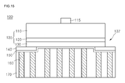
- Fig. 1 is a side-sectional view of a semiconductor light emitting device according to one embodiment.
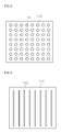
- Figs. 2 to 5 are diagrams illustrating the pattern of a first buffer member according to embodiments.
- Figs. 6 to 15 are diagrams illustrating a method for fabricating a semiconductor light emitting device according to one embodiment.
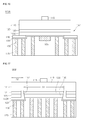
- Fig. 16 is a side-sectional view illustrating a semiconductor light emitting device according to another embodiment.
- Fig. 17 is a diagram illustrating a semiconductor light emitting device according to another embodiment.
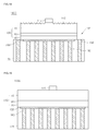
- Fig. 18 is a diagram illustrating a semiconductor light emitting device according to another embodiment.
- Fig. 19 is a diagram illustrating a semiconductor light emitting device according to another embodiment.
- Fig. 20 is a side-sectional view illustrating a light emitting device package according to another embodiment.
- Fig. 1 is a side-sectional view of a semiconductor light emitting device according to one embodiment.
- a semiconductor light emitting device 100 includes a plurality of compound semiconductor layers 135, a channel layer 140, an electrode layer 150, a first buffer member 160, a conductive support member 170, and an electrode 115.
- the plurality of compound semiconductor layers 135 are formed of the compound semiconductor of group III-V elements, and include a first conductive semiconductor layer 110, an active layer 120 and a second conductive semiconductor layer 130.
- the first conductive semiconductor layer 110 may be formed of an N-type semiconductor on which a first conductive dopant is doped.
- the N-type semiconductor may consist of any one of compound semiconductors such as GaN, InN, AlN, InGaN, AlGaN, InAlGaN and AlInN.
- the first conductive dopant includes Si, Ge, Sn, Se and Te.
- the active layer 120 is formed under the first conductive semiconductor layer 110, and the active layer 120 may be formed in a single quantum well structure or a multiple quantum well structure.
- the active layer 120 for example, may be formed in a single quantum well structure or a multiple quantum well structure for each period of an InGaN well layer/GaN barrier layer.
- the material of a quantum well layer and the material of a quantum barrier layer may be changed according to light emitting materials, but the active layer 120 is not limited thereto.
- a clad layer may be formed on or/and under the active layer 120.
- the second conductive semiconductor layer 130 is formed under the active layer 120, and may be formed of a P-type semiconductor on which a second conductive dopant is doped.
- the P-type semiconductor may consist of any one of compound semiconductors such as GaN, InN, AlN, InGaN, AlGaN, InAlGaN and AlInN.
- the second conductive dopant may include an element such as Mg, Be and Ze.
- the first conductive semiconductor layer 110, the active layer 120 and the second conductive semiconductor layer 130 may be defined as a light emitting structure.
- a third conductive semiconductor layer having a opposite polarity to that of the second conductive semiconductor layer 130 is formed on the second conductive semiconductor layer 130, and the third conductive semiconductor layer (not shown) may be formed as an N-type semiconductor layer.
- the first conductive semiconductor layer 110 may be formed of a P-type semiconductor
- the second conductive semiconductor layer 130 may be formed of an N-type semiconductor. Consequently, the light emitting structure may include any one of an N-P junction structure, a P-N junction structure, an N-P-N junction structure and a P-N-P junction structure.
- the second conductive semiconductor layer 130 will be described as an example of the lowermost layer of the compound semiconductor layers 135.
- the channel layer 140 may be formed at the lower-surface perimeter of the second conductive semiconductor layer 130.
- the channel layer 140 may be formed of a conductive material or an insulating material which selectively includes an oxide and a nitride, and may be formed of a material that is selected from among Indium Tin Oxide (ITO), Indium Zinc Oxide (IZO), Indium Zinc Tin Oxide (IZTO), Indium Aluminum Zinc Oxide (IAZO), Indium Gallium Zinc Oxide (IGZO), Indium Gallium Tin Oxide (IGTO), Aluminum Zinc Oxide (AZO), Antimony Tin Oxide (ATO), Gallium Zinc Oxide (GZO), SiO 2 , SiO x , SiO x N y , Si 3 N 4 , Al 2 O 3 and TiO 2 .
- the channel layer 140 may not be formed.
- the electrode layer 150 is formed under the second conductive semiconductor layer 130.
- the electrode layer 150 may be formed of at least one of Ag, Ni, Al, Rh, Pd, Ir, Ru, Mg, Zn, Pt, Au, Hf and a material consisting of their selective combination.
- the electrode layer 150 may be formed of a reflection electrode material having ohmic characteristic. A material having ohmic characteristic may be formed between the electrode layer 150 and the second conductive semiconductor layer 130 in a certain pattern, but it is not limited thereto.
- the electrode layer 150 may be formed of an oxide or nitride-based conductive material, for example, may be formed of a material that is selected from among ITO, Indium Tin Oxide Nitride (ITON), IZO, Indium Zinc Oxide Nitride (IZON), IZTO, IAZO, IGZO, IGTO, AZO, ATO, GZO, IrO x , RuO x and NiO.
- the electrode layer 150 may serve as a current spreading layer that may spread a current. Moreover, the electrode layer 150 may be a reflection electrode layer, and may include a metal layer of a single-layer structure or a multiple-layer structure.
- a current blocking layer may be formed between the electrode layer 150 and the second conductive semiconductor layer 130.
- the current blocking layer may be formed of a material that is an oxide or an insulating material and has lower conductivity than that of the material of the electrode layer 150.
- the current blocking layer is formed in a pattern form.
- the conductive support member 170 may be formed under the electrode layer 150, and the conductive support member 170 may be formed of a material such as Cu, Au, Ni and Mo.
- the thickness of the conductive support member 170 may be formed to about 10 ⁇ m to about 300 ⁇ m.
- the conductive support member 170 comprises a material having a thermal expansion coefficient of about Ni(Nickel) 13 ⁇ 10 -6 /K, and Cu (Copper) 16 ⁇ 10 -6 /K.
- the first buffer member 160 is embedded together with a plurality of cores or wicks, in the conductive support member 170.
- the first buffer member 160 may be formed under the electrode layer 150 in a certain pattern.
- the first buffer member 160 may be formed by selectively using a material having certain stiffness, a refractory material and a nonconductive material, for example, may be formed of any one of SiO 2 , Si 3 N 4 , Al 2 0 3 , Ti0 2 , SiO x , SiN x 2, SiN x , SiO x N y and a photoresist.
- the first buffer member 160 may be formed of a nonconductive material having a thermal expansion coefficient same to or similar to that of the conductive support member 170.
- the first buffer member 160 comprises a material having a thermal expansion coefficient less than a thermal expansion coefficient of the conductive support member 170.
- the first buffer member 160 comprises a material having a thermal expansion coefficient of about 0.5 ⁇ 8 ⁇ 10 -6 /K.
- the first buffer member 160 comprises a material having a Young's Modulus of about 72 ⁇ 390 Gpa.
- the height of the insulating material 160 may be the same as the thickness of the conductive support member 170, or may be formed to have a length greater than about the 50 % of the thickness of the conductive support member 170.
- the bottom of the first buffer member 160 may be exposed to a lower portion.
- the first buffer member 160 may have different heights according to a disposed region, but it is not limited thereto.
- the height of the first buffer member 160 may be determined with respect to the bottom of the conductive support member 170, or may be determined with respect to the bottom of the electrode layer 150.
- the first buffer member 160 may be spaced apart to conformally be disposed at an entire region and be formed in a certain type of pattern. As illustrated in FIGS. 2 to 5 , the pattern type of the first buffer member 160 may be formed in a dot matrix type using a pillar shape such as a circular pillar or a multi-angle pillar. Moreover, the first buffer member 160 may be formed in a stripe type using a plurality of bar types. The first buffer member 160 may be formed in a pattern (for example, a cross type or a line matrix type) that is crossed at least one time. Such a type may be modified.
- the first buffer member 160 is disposed in the conductive support member 170 to have certain intervals.
- the first buffer member 160 perpendicularly passes through the conductive support member 170, and is arranged at regular or irregular intervals in a horizontal direction, in the conductive support member 170.
- the first buffer member 160 may be formed to have intervals, which are greater than about 30 ⁇ m, between patterns. The interval may become broader in proportion to the thickness of the conductive support member 170.
- the pattern diameter of the first buffer member 160 may be formed to about 10 ⁇ m or greater.
- the first buffer member 160 and the conductive support member 170 can provide certain stiffness to the lower portion of a Light Emitting Diode (LED) chip.
- LED Light Emitting Diode
- the first buffer member 160 and the conductive support member 170 prevent the LED chip from being bent by an impulse that is given to the electrode 115.
- the first buffer member 160 can prevent the LED chip from being bent by heat that is generated in the LED chip, and can improve limitations in which the LED chip is broken or detached and thereby degrades chip characteristic.
- Figs. 2 to 5 are diagrams illustrating the pattern of a first buffer member according to embodiments.
- the first buffer member 160 has a pattern, having a certain size and a tetragonal pillar shape, which is disposed at certain intervals inside the conductive support member 170, wherein the disposition of the pattern may be made at regular intervals or irregular intervals.
- the first buffer member 160 may be arranged in a dot matrix type having a multi-angle pillar shape such as a triangular pillar and a tetragonal pillar.
- a first buffer member 161 has a pattern, having a certain size and a circular pillar shape, which is disposed at certain intervals inside the conductive support member 170, wherein the disposition of the pattern may be made at regular intervals or irregular intervals.
- the first buffer member 161 may be arranged in a dot matrix type having a pillar shape, which has a certain curvature, such as a circular pillar and an elliptical pillar.
- a first buffer member 162 may be formed of a bar shapes having a certain size disposed in a stripe type inside the conductive support member 170, wherein the bar shapes may be formed at regular intervals or irregular intervals. Moreover, the cross-sectional surface of the first buffer member 162 may have a tetragonal pillar or a domed shape, but it is not limited thereto.
- the first buffer member 160 may be formed in a line matrix type where patterns having a certain length and a bar shape are perpendicularly crossed, inside the conductive support member 170.
- the patterns of the stripe type may be crossed perpendicularly or at a certain angle, but it is not limited thereto.
- Figs. 6 to 15 are diagrams illustrating a method for fabricating a semiconductor light emitting device according to one embodiment.
- a plurality of compound semiconductor layers 135 are formed on a substrate 101.
- the substrate 101 may be selected from the group consisting of sapphire substrate (Al 2 O 3 ), GaN, SiC, ZnO, Si, GaP, InP, Ga 2 O 3 and GaAs.
- a concave-convex pattern may be formed on the substrate 101.
- a nitride semiconductor is grown on the substrate 101.
- growth equipment may use an electron beam evaporator or a dual-type thermal evaporator, and the nitride semiconductor may be formed by electron beam evaporator, Physical Vapor Deposition (PVD), Chemical Vapor Deposition (CVD), Plasma Laser Deposition (PLD), dual-type thermal evaporator, sputtering and Metal Organic Chemical Vapor Deposition (MOCVD), but it is not limited thereto.
- PVD Physical Vapor Deposition
- CVD Chemical Vapor Deposition
- PLD Plasma Laser Deposition
- MOCVD Metal Organic Chemical Vapor Deposition
- a buffer layer or/and an undoped semiconductor layer may be formed with the compound semiconductor of group II to group VI elements on the substrate 101, and may be removed after a thin film grows.
- the buffer layer decreases lattice constant difference between the substrate 101 and the nitride semiconductor, and the undoped semiconductor layer may be formed of GaN that is not intentionally doped.
- a semiconductor for extracting the dislocation defect of a compound semiconductor or light may be formed on the substrate 101, but it is not limited thereto.
- the plurality of compound semiconductor layers 135 are formed on the substrate 101, and the plurality of compound semiconductor layers 135 may serve as a light emitting structure.
- the plurality of compound semiconductor layers 135 include a first conductive semiconductor layer 110, an active layer 120 and a second conductive semiconductor layer 130.
- the active layer 120 is formed on the first conductive semiconductor layer 110, and the second conductive semiconductor layer 130 is formed on the active layer 120.
- the first conductive semiconductor layer 110, the active layer 120 and the second conductive semiconductor layer 130 may be formed of the compound semiconductor of group III-V elements, and each of the layers 110, 120 and 130 may be formed to have at least one layer or multiple-layer.
- the first conductive semiconductor layer 110 may be formed as a semiconductor layer on which a first conductive dopant is doped, and the second conductive semiconductor layer 130 may be formed as a semiconductor layer on which a second conductive dopant is doped.
- the first conductive semiconductor layer 110 selectively includes compound semiconductors such as GaN, InN, AlN, InGaN, AlGaN, InAlGaN and AlInN.
- the first conductive dopant includes an N-type dopant such as Si, Ge, Sn, Se and Te.
- the second conductive semiconductor layer 130 selectively includes compound semiconductors such as GaN, InN, AlN, InGaN, AlGaN, InAlGaN and AlInN.
- the second conductive dopant may include a P-type dopant such as Mg.
- Another semiconductor layer may be formed on or/and under each of the layers 110, 120 and 130, but it is not limited thereto.
- a third conductive semiconductor layer having a opposite polarity to that of the second conductive semiconductor layer 130 is formed on the second conductive semiconductor layer 130, and the third conductive semiconductor layer (not shown) may be formed as an N-type semiconductor layer or a P-type semiconductor layer.
- the plurality of compound semiconductor layers 135 may include any one of an N-P junction structure, a P-N junction structure, an N-P-N junction structure and a P-N-P junction structure.
- the channel layer 140 may be formed of a conductive material or an insulating material which selectively includes an oxide and a nitride, and may be formed of a material that is selected from among ITO, IZO, IZTO, IAZO, IGZO, IGTO, AZO, ATO, GZO, SiO 2 , SiO x , SiO x N y , Si 3 N 4 , Al 2 O 3 and TiO 2 .
- the channel layer 140 may not be formed.
- the channel layer 140 improves adhesiveness to the second conductive semiconductor layer 130, thereby minimizing exfoliation. Moreover, when the channel layer 140 is formed of an insulating material, it can separate the second conductive semiconductor layer 130 and a metal material such as a conductive support member. When the channel layer 140 is formed of a conductive material, it improves current flow, thereby decreasing a driving voltage.
- an electrode layer 150 may be formed at a portion or entirety of a region on the second conductive semiconductor layer 130.
- the electrode layer 150 may include a material having at least one characteristic of a seed metal, an ohmic metal and a reflection metal.
- the electrode layer 150 for example, may be formed of at least one of Ag, Ni, Al, Rh, Pd, Ir, Ru, Mg, Zn, Pt, Au, Hf and a material consisting of their selective combination.
- the electrode layer 150 may be extended to a portion or entire upper surface of the channel layer 140.
- a first buffer member 160 is formed on the electrode layer 150.
- the first buffer member 160 may be formed in any one of sputtering, electron beam evaporation, CVD and Plasma Enhanced Chemical Vapor Deposition (PECVD).
- the first buffer member 160 may be formed in certain patterns, which are spaced at certain intervals, on the electrode layer 150.
- the first buffer member 160 may be formed by selectively using a material having certain stiffness, a refractory material and an insulating material, for example, may be formed of any one of Si0 2 , Si 3 N 4 , Al 2 0 3 , TiO 2 , SiO x , SiN x 2, SiN x , SiO x N y and a photoresist.
- the height 'T1' of the first buffer member 160 may be formed to about 10 ⁇ m to about 300 ⁇ m.
- the height 'T1' of the first buffer member 160 may be formed to a certain length from the upper surface of the electrode layer 140 that is disposed on the second conductive semiconductor layer 130.
- the lower surface of the first buffer member 160 may be disposed at different planes.
- the pattern of the first buffer member 160 may include the pattern types as illustrated Figs. 2 to 5 .
- the pattern may be formed in a dot matrix type using a pillar shape, a stripe type, a type having a plurality of domed shapes, a type having a plurality of concentric circle shapes, or a pattern type (for example, a cross shape or a matrix type) that is crossed at least one time. These pattern types may be modified.
- a conductive support member 170 may be formed on the electrode layer 150.
- the conductive support member 170 is formed in an electro plating process, and may be formed of a material such as Cu, Au, Ni and Mo.
- the first buffer member 160 is disposed at the inner region of the conductive support member 170.
- the first buffer member 160 has a type in which it perpendicularly passes through the conductive support member 170, and is arranged at certain intervals and in a horizontal direction.
- the thickness of the conductive support member 170 may be to the same height 'T1' as that of the first buffer member 160.
- the conductive support member 170 and the first buffer member 160 can provide electrical reliability when an upper surface, i.e., a base surface in a chip becomes a flat plane.
- the upper end of the conductive support member 170 and the upper end of the first buffer member 160 may be disposed at the same plane or different planes.
- the conductive support member 170 and the first buffer member 160 are cut to have the thickness 'T2'.
- the conductive support member 170 and the first buffer member 160 are cut to have a thickness 'T0' less than the thickness of the conductive support member 170 or may be planarized in a polishing process.
- the conductive support member 170 when the thickness 'T4' of the conductive support member 170 is greater than the height 'T3' of the first buffer member 160, the conductive support member 170 is cut to have a thickness equal to or less than the height 'T3' of the first buffer member 160 or may be planarized in a polishing process.
- the substrate (101 in Fig. 9 ) is removed by a physical or/and chemical removing process.
- a process of removing the substrate (110 in Fig. 10 ) may use a Laser Lift Off (LLO) process that radiates laser, having a wavelength of a certain region, to the substrate 101, and separates the substrate 101.
- LLO Laser Lift Off
- the substrate 101 may be separated by removing the buffer layer with a wet etching liquid.
- a process using an Inductively coupled Plasma/Reactive Ion Etching (ICP/RCE) process may be performed on the surface of the first conductive semiconductor layer 110 from which the substrate 101 has been removed.
- ICP/RCE Inductively coupled Plasma/Reactive Ion Etching
- a chip boundary region i.e., a channel region
- the channel spacer 137 of the plurality of compound semiconductor layers 135 is formed.
- the outer side of the channel layer 140 is exposed through the channel spacer 137.
- an electrode having a certain pattern is formed on the first conductive semiconductor layer 110.
- a process of forming the electrode 115 may be performed before/after the isolation etching or may be performed after a chip is separated, but it is not limited thereto.
- the electrode 115 may include at least one electrode pad, and the pattern of a branch structure for current spreading may be connected to the electrode pad.
- a structure for improving light extraction efficiency may be formed at the upper surface of the first conductive semiconductor layer 110.
- the structure is separated through a process such as breaking or/and cutting in the size of chip unit.
- a wire may be bonded to the electrode 115.
- the first buffer member 160 absorbs or supports a chip from an impulse that is given to the electrode 115.
- the first buffer member 160 can prevent a wafer from being bent, and moreover, can remove limitations in which the plurality of compound semiconductor layers 135 are bent. Furthermore, the first buffer member 160 prevents the LED chip from being bent by heat that is generated in the LED chip.
- Fig. 16 is a side-sectional view illustrating a semiconductor light emitting device according to another embodiment.
- the same elements as those of the above-described embodiment will reference one embodiment.
- a semiconductor light emitting device 100A includes a first conductive semiconductor layer 110, an active layer 120, a second conductive semiconductor layer 130, a channel layer 140, an electrode layer 150, a first buffer member 160, a second buffer member 165, a conductive support member 170, and an electrode 115.
- the first buffer member 160, the second buffer member 165 and the conductive support member 170 may be formed under the electrode layer 150.
- the first buffer member 160 is formed in a certain pattern at the bottom of the electrode layer 150. At least one portion of the second buffer member 165 may be disposed to perpendicularly overlap with the electrode 115.
- the first buffer member 160 may be formed in the pattern shapes (which are as illustrated Figs. 2 to 5 ) at a region other than the second buffer member 165, in the conductive support member 170.
- the second buffer member 165 is formed for protecting an LED chip from a direct impulse, and is formed in correspondence with the formed position of the electrode 115.
- the second buffer member 165 may selectively include an insulating material, a refractory metal and a conductive metal of high stiffness, for example, may be selected from among materials such as Si0 2 , Si 3 N 4 , Al 2 0 3 , TiO 2 , SiO x , SiN x 2, SiN x , SiO x N y , a photoresist, W and Mo.
- the second buffer member 165 may be formed to have at least a thickness of about 1 ⁇ m.
- the second buffer member 165 may be formed to a thickness of about 1 ⁇ m to about 10 ⁇ m.
- the second buffer member 165 may be formed to have the same number as the number of electrodes or patterns, or may be formed in the same pattern.
- the electrode 115 includes an electrode pad.
- the second buffer member 165 supports the lower portion of a chip from an impulse that is given by the electrode 115, and suppresses the bending of the semiconductor layers 110, 120 and 130. Accordingly, the second buffer member 165 can improve limitations in which a finally-completed LED chip is broken or exfoliated and thereby chip characteristic is degraded.
- Fig. 17 is a diagram illustrating a semiconductor light emitting device according to another embodiment.
- the same elements as those of the above-described embodiments will reference the embodiments.
- a semiconductor light emitting device 100B includes a first conductive semiconductor layer 110, an active layer 120, a second conductive semiconductor layer 130, a channel layer 140A, an electrode layer 150, a first buffer member 160, a conductive support member 170, and an electrode 115.
- the channel layer 140A is formed in a frame shape at the lower-surface perimeter of the second conductive semiconductor layer 130.
- An insulating protrusion 147 is formed at the channel layer 140A, and the insulating protrusion 147 electrically deactivates the outer sides 111, 121 and 131 of the plurality of compound semiconductor layers 110, 120 and 130.
- the insulating protrusion 147 may be formed in a belt shape, a ring shape or a frame shape.
- the channel layer 140A is formed of an insulating material, for example, Si0 2 , SiO x , SiO x N y , Si 3 N 4 and Al 2 0 3 .
- the insulating protrusion 147 divides the inner region 'A1' and outer region 'A2' of the plurality of compound semiconductor layers 110, 120 and 130.
- the inner region 'A1' is an active region
- the outer region 'A2' is an inactive region. Accordingly, the compound semiconductor layers 110, 120 and 130 that are disposed at the active region enable the semiconductor light emitting device to normally operate although each of the layers of outer walls becomes short due to moisture.
- the formed position of the insulating protrusion 147 may be changed to the outer wall of a chip or a position internal to the outer wall.
- the insulating protrusion 147 can enhance the adhesive strength between the compound semiconductor layers 110, 120 and 130 and the channel 140A.
- Fig. 18 is a diagram illustrating a semiconductor light emitting device according to another embodiment.
- the same elements as those of the above-disclosed embodiments will reference the embodiments.
- a semiconductor light emitting device 100C includes a first conductive semiconductor layer 110, an active layer 120, a second conductive semiconductor layer 130, an electrode layer 150, a first buffer member 160, a conductive support member 170, and an electrode 115.
- a certain roughness 112 may be formed at the upper surface of the first conductive semiconductor layer 110, but the pattern of the roughness 112 is not limited to that of Fig. 18 .
- a channel layer (140 of Fig. 1 ) may not be formed under the second conductive semiconductor layer 130, or the electrode layer 150 may be formed.
- the conductive support member 170 and the first buffer member 160 may be formed on the electrode layer 150 to have the same thickness.
- the electrode layer 150 is formed at the inner region of the second conductive semiconductor layer 130, and may be formed not to be exposed to the channel spacer 137 of the compound semiconductor layer 135. Accordingly, a portion of the first buffer member 160 may be formed under the second conductive semiconductor layer 130. At least one of the first buffer member 160 may be exposed to the outer side of the plurality of compound semiconductor layers 135.
- the first buffer member 160 can prevent an LED chip from being bent under the second conductive semiconductor layer 130 by an external impulse or heat.
- Fig. 19 is a diagram illustrating a semiconductor light emitting device according to another embodiment.
- the same elements as those of the above-disclosed embodiments will reference the embodiments.
- a semiconductor light emitting device 100D includes a first conductive semiconductor layer 110, an active layer 120, a second conductive semiconductor layer 130, an electrode layer 150, a first buffer member 160, a conductive support member 170, and an electrode 115.
- a cutting spacer may not be formed at the outer walls of a plurality of compound semiconductor layers 135, and the compound semiconductor layer 135 and the conductive support member 170 may be formed to have the same diameter.
- a feature in which a first buffer member is disclosed may be applied to the substrate of a lateral semiconductor light emitting device as well as the substrate of a vertical semiconductor light emitting device.
- Fig. 20 is a side-sectional view illustrating a light emitting device package according to another embodiment.
- a light emitting device package 200 includes a body 210, first and second lead electrodes 211 and 213 disposed at the body 210, a light emitting device 100 according to embodiment(s), and a molding member 220 surrounding the light emitting device 100.
- the light emitting device 100 is disposed at the body 210 and is electrically connected to the first and second lead electrodes 211 and 213.
- the body 210 may be formed of include silicon, plastic or metal.
- a cavity 205 having an inclined surface may be formed around the light emitting device 100.
- the first and second lead electrodes 211 and 213 are electrically disconnected, and supply a power source to the light emitting device 100. Moreover, the first and second lead electrodes 211 and 213 reflect light that is produced from the light emitting device 100, thereby enhancing light efficiency. The first and second lead electrodes 211 and 213 may release heat, which is produced from the light emitting device 100, to the outside.
- the light emitting device 100 may be disposed on the body 210, or may be disposed on the first lead electrode 211 or the second lead electrode 213.
- the light emitting device 100 may be electrically connected to the second lead electrode 213 through a wire 202, and may be connected to the first lead electrode 211 in a die bonding type.
- the molding member 220 surrounds the light emitting device 100, thereby protecting the light emitting device 100. Moreover, a phosphor is included in the molding member 220, and it can vary the wavelength of light that is emitted from the light emitting device 100.
- the semiconductor light emitting device is connected to the first and second lead electrodes and is packaged, thereby being used as the light sources of pointing devices, illumination devices like as a lamp and a streetlight, light unit, lighting devices and display devices.
- each of the embodiments is not limited to it, and may be selectively applied to but is not limited to the above-described other embodiment.
- the method of fabricating the semiconductor light emitting device includes forming a plurality of compound semiconductor layers including an active layer and a second conductive semiconductor layer; forming an electrode layer on the second conductive semiconductor layer; forming a plurality of first buffer members having the type of patterns spaced apart, on the electrode layer; forming a conductive support member between the first buffer members, on the electrode layer.
- the semiconductor light emitting device can protect the light emitting structure from an external impulse.
- the semiconductor light emitting device can prevent the characteristic of an LED chip from being degraded by an impulse.
- the semiconductor light emitting device can minimize the bending of the LED chip due to heat.
- any reference in this specification to "one embodiment,” “an embodiment,” “example embodiment,” etc. means that a particular feature, structure, or characteristic described in connection with the embodiment is included in at least one embodiment of the invention.
- the appearances of such phrases in various places in the specification are not necessarily all referring to the same embodiment.
Landscapes
- Led Devices (AREA)
Abstract

Description
- The present application claims priority to Korean Patent Application No.
10-2009-0013605 (filed on February 18, 2009 - The present disclosure relates to a semiconductor light emitting device and a light emitting device package having the same.
- Group III-V nitride semiconductors have been variously applied to an optical device such as blue and green Light Emitting Diodes (LED), a high speed switching device such as a Metal Oxide Semiconductor Field Effect Transistor (MOSFET), a High Electron Mobility Transistor (HEMT) and a Hetero junction Field Effect Transistor (HFET), and a light source of a lighting device or a display device.
- The nitride semiconductor is mainly used for the LED or a Laser Diode (LD), and studies have been continuously conducted to improve the manufacturing process or light efficiency of the nitride semiconductor.
- Embodiments provide a semiconductor light emitting device, which can prevent the contortion of a wafer.
- Embodiments provide a semiconductor light emitting device, which includes a first buffer member in a conductive support member disposed under a compound semiconductor layer.
- Embodiments provide a light emitting device package including a light emitting device having a first buffer member in a conductive support member.
- An embodiment provides a semiconductor light emitting device comprising: a plurality of compound semiconductor layers comprising a first conductive semiconductor layer, an active layer and a second conductive semiconductor layer; an electrode layer under the plurality of compound semiconductor layers; a conductive support member under the electrode layer; and a first buffer member embedded to be spaced apart, in the conductive support member.
- An embodiment provides a semiconductor light emitting device comprising: a plurality of compound semiconductor layers comprising a first conductive semiconductor layer, an active layer and a second conductive semiconductor layer; an electrode layer disposed under the plurality of compound semiconductor layers, and electrically connected to the second conductive semiconductor layer; an electrode electrically connected to the first conductive semiconductor layer; a conductive support member under the electrode layer; and a first buffer member arranged in the conductive support member to have a height equal to or less than a thickness of the conductive support member.
- An embodiment provides a semiconductor light emitting device package comprising: a body; a plurality of lead electrodes in the body; a light emitting device electrically connected to the plurality of lead electrodes; and a molding member covering the light emitting device, wherein the light emitting device comprises: a plurality of compound semiconductor layers comprising a first conductive semiconductor layer, an active layer and a second conductive semiconductor layer; an electrode layer under the plurality of compound semiconductor layers; a conductive support member under the electrode layer; and a first buffer member embedded to be spaced apart, in the conductive support member.
- The details of one or more embodiments are set forth in the accompanying drawings and the description below. Other features will be apparent from the description and drawings, and from the claims.
-
Fig. 1 is a side-sectional view of a semiconductor light emitting device according to one embodiment. -
Figs. 2 to 5 are diagrams illustrating the pattern of a first buffer member according to embodiments. -
Figs. 6 to 15 are diagrams illustrating a method for fabricating a semiconductor light emitting device according to one embodiment. -
Fig. 16 is a side-sectional view illustrating a semiconductor light emitting device according to another embodiment. -
Fig. 17 is a diagram illustrating a semiconductor light emitting device according to another embodiment. -
Fig. 18 is a diagram illustrating a semiconductor light emitting device according to another embodiment. -
Fig. 19 is a diagram illustrating a semiconductor light emitting device according to another embodiment. -
Fig. 20 is a side-sectional view illustrating a light emitting device package according to another embodiment. - Reference will now be made in detail to the embodiments of the present disclosure, examples of which are illustrated in the accompanying drawings. In description of embodiments, the 'on' or 'under' of each layer may be described with reference to the accompanying drawings, and the thickness of the each layer will also be described as an example and is not limited to the thickness of the accompanying drawings.
- In description of embodiments, it will be understood that in a case where a layer (or film), a region, a pattern, or components is referred to as being 'on' or 'under' another substrate, layer (or film), region or patterns, the 'on' and 'under' include all the meanings of 'directly' and 'indirectly'. Moreover, any reference of the 'on' or 'under' of each layer will be described with reference to the accompanying drawings.
-
Fig. 1 is a side-sectional view of a semiconductor light emitting device according to one embodiment. - Referring to
Fig. 1 , a semiconductorlight emitting device 100 according to one embodiment includes a plurality ofcompound semiconductor layers 135, achannel layer 140, anelectrode layer 150, afirst buffer member 160, aconductive support member 170, and anelectrode 115. - The plurality of
compound semiconductor layers 135 are formed of the compound semiconductor of group III-V elements, and include a firstconductive semiconductor layer 110, anactive layer 120 and a secondconductive semiconductor layer 130. - The first
conductive semiconductor layer 110 may be formed of an N-type semiconductor on which a first conductive dopant is doped. The N-type semiconductor may consist of any one of compound semiconductors such as GaN, InN, AlN, InGaN, AlGaN, InAlGaN and AlInN. As the N-type dopant, the first conductive dopant includes Si, Ge, Sn, Se and Te. - The
active layer 120 is formed under the firstconductive semiconductor layer 110, and theactive layer 120 may be formed in a single quantum well structure or a multiple quantum well structure. Theactive layer 120, for example, may be formed in a single quantum well structure or a multiple quantum well structure for each period of an InGaN well layer/GaN barrier layer. In theactive layer 120, the material of a quantum well layer and the material of a quantum barrier layer may be changed according to light emitting materials, but theactive layer 120 is not limited thereto. A clad layer may be formed on or/and under theactive layer 120. - The second
conductive semiconductor layer 130 is formed under theactive layer 120, and may be formed of a P-type semiconductor on which a second conductive dopant is doped. The P-type semiconductor may consist of any one of compound semiconductors such as GaN, InN, AlN, InGaN, AlGaN, InAlGaN and AlInN. As the P-type dopant, the second conductive dopant may include an element such as Mg, Be and Ze. - The first
conductive semiconductor layer 110, theactive layer 120 and the secondconductive semiconductor layer 130 may be defined as a light emitting structure. A third conductive semiconductor layer having a opposite polarity to that of the secondconductive semiconductor layer 130 is formed on the secondconductive semiconductor layer 130, and the third conductive semiconductor layer (not shown) may be formed as an N-type semiconductor layer. Moreover, the firstconductive semiconductor layer 110 may be formed of a P-type semiconductor, and the secondconductive semiconductor layer 130 may be formed of an N-type semiconductor. Consequently, the light emitting structure may include any one of an N-P junction structure, a P-N junction structure, an N-P-N junction structure and a P-N-P junction structure. In the following description on one embodiment, the secondconductive semiconductor layer 130 will be described as an example of the lowermost layer of thecompound semiconductor layers 135. - The
channel layer 140 may be formed at the lower-surface perimeter of the secondconductive semiconductor layer 130. Thechannel layer 140 may be formed of a conductive material or an insulating material which selectively includes an oxide and a nitride, and may be formed of a material that is selected from among Indium Tin Oxide (ITO), Indium Zinc Oxide (IZO), Indium Zinc Tin Oxide (IZTO), Indium Aluminum Zinc Oxide (IAZO), Indium Gallium Zinc Oxide (IGZO), Indium Gallium Tin Oxide (IGTO), Aluminum Zinc Oxide (AZO), Antimony Tin Oxide (ATO), Gallium Zinc Oxide (GZO), SiO2, SiOx, SiOxNy, Si3N4, Al2O3 and TiO2. Thechannel layer 140 may not be formed. - The
electrode layer 150 is formed under the secondconductive semiconductor layer 130. Theelectrode layer 150 may be formed of at least one of Ag, Ni, Al, Rh, Pd, Ir, Ru, Mg, Zn, Pt, Au, Hf and a material consisting of their selective combination. Moreover, theelectrode layer 150 may be formed of a reflection electrode material having ohmic characteristic. A material having ohmic characteristic may be formed between theelectrode layer 150 and the secondconductive semiconductor layer 130 in a certain pattern, but it is not limited thereto. - The
electrode layer 150 may be formed of an oxide or nitride-based conductive material, for example, may be formed of a material that is selected from among ITO, Indium Tin Oxide Nitride (ITON), IZO, Indium Zinc Oxide Nitride (IZON), IZTO, IAZO, IGZO, IGTO, AZO, ATO, GZO, IrOx, RuOx and NiO. - The
electrode layer 150 may serve as a current spreading layer that may spread a current. Moreover, theelectrode layer 150 may be a reflection electrode layer, and may include a metal layer of a single-layer structure or a multiple-layer structure. - A current blocking layer may be formed between the
electrode layer 150 and the secondconductive semiconductor layer 130. The current blocking layer may be formed of a material that is an oxide or an insulating material and has lower conductivity than that of the material of theelectrode layer 150. The current blocking layer is formed in a pattern form. - The
conductive support member 170 may be formed under theelectrode layer 150, and theconductive support member 170 may be formed of a material such as Cu, Au, Ni and Mo. The thickness of theconductive support member 170 may be formed to about 10 µm to about 300 µm. - The
conductive support member 170 comprises a material having a thermal expansion coefficient of about Ni(Nickel) 13×10-6/K, and Cu (Copper) 16×10-6/K. - The
first buffer member 160 is embedded together with a plurality of cores or wicks, in theconductive support member 170. Thefirst buffer member 160 may be formed under theelectrode layer 150 in a certain pattern. Thefirst buffer member 160 may be formed by selectively using a material having certain stiffness, a refractory material and a nonconductive material, for example, may be formed of any one of SiO2, Si3N4, Al203, Ti02, SiOx, SiNx2, SiNx, SiOxNy and a photoresist. Moreover, thefirst buffer member 160 may be formed of a nonconductive material having a thermal expansion coefficient same to or similar to that of theconductive support member 170. Thefirst buffer member 160 comprises a material having a thermal expansion coefficient less than a thermal expansion coefficient of theconductive support member 170. - The
first buffer member 160 comprises a material having a thermal expansion coefficient of about 0.5∼8×10⁻⁶/K. Thefirst buffer member 160 comprises a material having a Young's Modulus of about 72∼390 Gpa. - The height of the insulating
material 160 may be the same as the thickness of theconductive support member 170, or may be formed to have a length greater than about the 50 % of the thickness of theconductive support member 170. The bottom of thefirst buffer member 160 may be exposed to a lower portion. Thefirst buffer member 160 may have different heights according to a disposed region, but it is not limited thereto. Herein, the height of thefirst buffer member 160 may be determined with respect to the bottom of theconductive support member 170, or may be determined with respect to the bottom of theelectrode layer 150. - The
first buffer member 160 may be spaced apart to conformally be disposed at an entire region and be formed in a certain type of pattern. As illustrated inFIGS. 2 to 5 , the pattern type of thefirst buffer member 160 may be formed in a dot matrix type using a pillar shape such as a circular pillar or a multi-angle pillar. Moreover, thefirst buffer member 160 may be formed in a stripe type using a plurality of bar types. Thefirst buffer member 160 may be formed in a pattern (for example, a cross type or a line matrix type) that is crossed at least one time. Such a type may be modified. - The
first buffer member 160 is disposed in theconductive support member 170 to have certain intervals. Thefirst buffer member 160 perpendicularly passes through theconductive support member 170, and is arranged at regular or irregular intervals in a horizontal direction, in theconductive support member 170. - The
first buffer member 160 may be formed to have intervals, which are greater than about 30 µm, between patterns. The interval may become broader in proportion to the thickness of theconductive support member 170. The pattern diameter of thefirst buffer member 160 may be formed to about 10 µm or greater. - The
first buffer member 160 and theconductive support member 170 can provide certain stiffness to the lower portion of a Light Emitting Diode (LED) chip. For example, when a wire is bonded to theelectrode 115, thefirst buffer member 160 and theconductive support member 170 prevent the LED chip from being bent by an impulse that is given to theelectrode 115. Moreover, thefirst buffer member 160 can prevent the LED chip from being bent by heat that is generated in the LED chip, and can improve limitations in which the LED chip is broken or detached and thereby degrades chip characteristic. -
Figs. 2 to 5 are diagrams illustrating the pattern of a first buffer member according to embodiments. - Referring to
Fig. 2 , thefirst buffer member 160 has a pattern, having a certain size and a tetragonal pillar shape, which is disposed at certain intervals inside theconductive support member 170, wherein the disposition of the pattern may be made at regular intervals or irregular intervals. Moreover, thefirst buffer member 160 may be arranged in a dot matrix type having a multi-angle pillar shape such as a triangular pillar and a tetragonal pillar. - Referring to
Fig. 3 , afirst buffer member 161 has a pattern, having a certain size and a circular pillar shape, which is disposed at certain intervals inside theconductive support member 170, wherein the disposition of the pattern may be made at regular intervals or irregular intervals. Moreover, thefirst buffer member 161 may be arranged in a dot matrix type having a pillar shape, which has a certain curvature, such as a circular pillar and an elliptical pillar. - Referring to
Fig. 4 , afirst buffer member 162 may be formed of a bar shapes having a certain size disposed in a stripe type inside theconductive support member 170, wherein the bar shapes may be formed at regular intervals or irregular intervals. Moreover, the cross-sectional surface of thefirst buffer member 162 may have a tetragonal pillar or a domed shape, but it is not limited thereto. - Referring to
Fig. 5 , thefirst buffer member 160 may be formed in a line matrix type where patterns having a certain length and a bar shape are perpendicularly crossed, inside theconductive support member 170. The patterns of the stripe type may be crossed perpendicularly or at a certain angle, but it is not limited thereto. -
Figs. 6 to 15 are diagrams illustrating a method for fabricating a semiconductor light emitting device according to one embodiment. - Referring to
Fig. 6 , a plurality of compound semiconductor layers 135 are formed on asubstrate 101. - The
substrate 101 may be selected from the group consisting of sapphire substrate (Al2O3), GaN, SiC, ZnO, Si, GaP, InP, Ga2O3 and GaAs. A concave-convex pattern may be formed on thesubstrate 101. - A nitride semiconductor is grown on the
substrate 101. Herein, growth equipment may use an electron beam evaporator or a dual-type thermal evaporator, and the nitride semiconductor may be formed by electron beam evaporator, Physical Vapor Deposition (PVD), Chemical Vapor Deposition (CVD), Plasma Laser Deposition (PLD), dual-type thermal evaporator, sputtering and Metal Organic Chemical Vapor Deposition (MOCVD), but it is not limited thereto. - A buffer layer or/and an undoped semiconductor layer may be formed with the compound semiconductor of group II to group VI elements on the
substrate 101, and may be removed after a thin film grows. The buffer layer decreases lattice constant difference between thesubstrate 101 and the nitride semiconductor, and the undoped semiconductor layer may be formed of GaN that is not intentionally doped. A semiconductor for extracting the dislocation defect of a compound semiconductor or light may be formed on thesubstrate 101, but it is not limited thereto. - The plurality of compound semiconductor layers 135 are formed on the
substrate 101, and the plurality of compound semiconductor layers 135 may serve as a light emitting structure. The plurality of compound semiconductor layers 135 include a firstconductive semiconductor layer 110, anactive layer 120 and a secondconductive semiconductor layer 130. Theactive layer 120 is formed on the firstconductive semiconductor layer 110, and the secondconductive semiconductor layer 130 is formed on theactive layer 120. - The first
conductive semiconductor layer 110, theactive layer 120 and the secondconductive semiconductor layer 130 may be formed of the compound semiconductor of group III-V elements, and each of thelayers - The first
conductive semiconductor layer 110 may be formed as a semiconductor layer on which a first conductive dopant is doped, and the secondconductive semiconductor layer 130 may be formed as a semiconductor layer on which a second conductive dopant is doped. As an N-type semiconductor layer, the firstconductive semiconductor layer 110 selectively includes compound semiconductors such as GaN, InN, AlN, InGaN, AlGaN, InAlGaN and AlInN. The first conductive dopant includes an N-type dopant such as Si, Ge, Sn, Se and Te. As a P-type semiconductor layer, the secondconductive semiconductor layer 130 selectively includes compound semiconductors such as GaN, InN, AlN, InGaN, AlGaN, InAlGaN and AlInN. The second conductive dopant may include a P-type dopant such as Mg. - Another semiconductor layer may be formed on or/and under each of the
layers conductive semiconductor layer 130 is formed on the secondconductive semiconductor layer 130, and the third conductive semiconductor layer (not shown) may be formed as an N-type semiconductor layer or a P-type semiconductor layer. Moreover, the plurality of compound semiconductor layers 135 may include any one of an N-P junction structure, a P-N junction structure, an N-P-N junction structure and a P-N-P junction structure. - An
inner region 142 on the secondconductive semiconductor layer 130 is opened, and achannel layer 140 may be formed at the outer perimeter of the secondconductive semiconductor layer 130. Thechannel layer 140 may be formed of a conductive material or an insulating material which selectively includes an oxide and a nitride, and may be formed of a material that is selected from among ITO, IZO, IZTO, IAZO, IGZO, IGTO, AZO, ATO, GZO, SiO2, SiOx, SiOxNy, Si3N4, Al2O3 and TiO2. Thechannel layer 140 may not be formed. - The
channel layer 140 improves adhesiveness to the secondconductive semiconductor layer 130, thereby minimizing exfoliation. Moreover, when thechannel layer 140 is formed of an insulating material, it can separate the secondconductive semiconductor layer 130 and a metal material such as a conductive support member. When thechannel layer 140 is formed of a conductive material, it improves current flow, thereby decreasing a driving voltage. - Referring to
Fig. 7 , anelectrode layer 150 may be formed at a portion or entirety of a region on the secondconductive semiconductor layer 130. Theelectrode layer 150 may include a material having at least one characteristic of a seed metal, an ohmic metal and a reflection metal. Theelectrode layer 150, for example, may be formed of at least one of Ag, Ni, Al, Rh, Pd, Ir, Ru, Mg, Zn, Pt, Au, Hf and a material consisting of their selective combination. Theelectrode layer 150 may be extended to a portion or entire upper surface of thechannel layer 140. - Referring to
Fig. 8 , afirst buffer member 160 is formed on theelectrode layer 150. Thefirst buffer member 160 may be formed in any one of sputtering, electron beam evaporation, CVD and Plasma Enhanced Chemical Vapor Deposition (PECVD). Thefirst buffer member 160 may be formed in certain patterns, which are spaced at certain intervals, on theelectrode layer 150. Thefirst buffer member 160 may be formed by selectively using a material having certain stiffness, a refractory material and an insulating material, for example, may be formed of any one of Si02, Si3N4, Al203, TiO2, SiOx, SiNx2, SiNx, SiOxNy and a photoresist. - The height 'T1' of the
first buffer member 160 may be formed to about 10 µm to about 300 µm. Herein, the height 'T1' of thefirst buffer member 160 may be formed to a certain length from the upper surface of theelectrode layer 140 that is disposed on the secondconductive semiconductor layer 130. The lower surface of thefirst buffer member 160 may be disposed at different planes. - The pattern of the
first buffer member 160 may include the pattern types as illustratedFigs. 2 to 5 . For example, the pattern may be formed in a dot matrix type using a pillar shape, a stripe type, a type having a plurality of domed shapes, a type having a plurality of concentric circle shapes, or a pattern type (for example, a cross shape or a matrix type) that is crossed at least one time. These pattern types may be modified. - Referring to
Fig. 9 , aconductive support member 170 may be formed on theelectrode layer 150. Theconductive support member 170 is formed in an electro plating process, and may be formed of a material such as Cu, Au, Ni and Mo. - The
first buffer member 160 is disposed at the inner region of theconductive support member 170. Thefirst buffer member 160 has a type in which it perpendicularly passes through theconductive support member 170, and is arranged at certain intervals and in a horizontal direction. - The thickness of the
conductive support member 170 may be to the same height 'T1' as that of thefirst buffer member 160. Theconductive support member 170 and thefirst buffer member 160 can provide electrical reliability when an upper surface, i.e., a base surface in a chip becomes a flat plane. - Herein, the upper end of the
conductive support member 170 and the upper end of thefirst buffer member 160 may be disposed at the same plane or different planes. - As illustrated in
Fig. 10 , when the height 'T1' of thefirst buffer member 160 is greater than the thickness 'T2' of theconductive support member 170, theconductive support member 170 and thefirst buffer member 160 are cut to have the thickness 'T2'. Alternatively, as illustrated inFig. 11 , theconductive support member 170 and thefirst buffer member 160 are cut to have a thickness 'T0' less than the thickness of theconductive support member 170 or may be planarized in a polishing process. - As illustrated in
Fig. 12 , when the thickness 'T4' of theconductive support member 170 is greater than the height 'T3' of thefirst buffer member 160, theconductive support member 170 is cut to have a thickness equal to or less than the height 'T3' of thefirst buffer member 160 or may be planarized in a polishing process. - Referring to
Figs. 6 and13 , when theconductive support member 170 is formed, the substrate (101 inFig. 9 ) is removed by a physical or/and chemical removing process. A process of removing the substrate (110 inFig. 10 ) may use a Laser Lift Off (LLO) process that radiates laser, having a wavelength of a certain region, to thesubstrate 101, and separates thesubstrate 101. - When another semiconductor layer (for example, a buffer layer) is formed between the
substrate 101 and the firstconductive semiconductor layer 110, thesubstrate 101 may be separated by removing the buffer layer with a wet etching liquid. A process using an Inductively coupled Plasma/Reactive Ion Etching (ICP/RCE) process may be performed on the surface of the firstconductive semiconductor layer 110 from which thesubstrate 101 has been removed. - Referring to
Figs. 13 and 14 , a chip boundary region (i.e., a channel region) is removed by isolation etching, and thereby thechannel spacer 137 of the plurality of compound semiconductor layers 135 is formed. The outer side of thechannel layer 140 is exposed through thechannel spacer 137. - Referring to
Fig. 15 , an electrode having a certain pattern is formed on the firstconductive semiconductor layer 110. Herein, a process of forming theelectrode 115 may be performed before/after the isolation etching or may be performed after a chip is separated, but it is not limited thereto. Theelectrode 115 may include at least one electrode pad, and the pattern of a branch structure for current spreading may be connected to the electrode pad. - A structure for improving light extraction efficiency may be formed at the upper surface of the first
conductive semiconductor layer 110. - Subsequently, the structure is separated through a process such as breaking or/and cutting in the size of chip unit.
- In the
light emitting device 100, a wire may be bonded to theelectrode 115. When the wire is bonded at the lower portion of a device, thefirst buffer member 160 absorbs or supports a chip from an impulse that is given to theelectrode 115. Thefirst buffer member 160 can prevent a wafer from being bent, and moreover, can remove limitations in which the plurality of compound semiconductor layers 135 are bent. Furthermore, thefirst buffer member 160 prevents the LED chip from being bent by heat that is generated in the LED chip. -
Fig. 16 is a side-sectional view illustrating a semiconductor light emitting device according to another embodiment. In the following description on another embodiment, the same elements as those of the above-described embodiment will reference one embodiment. - Referring to
Fig. 16 , a semiconductorlight emitting device 100A according to another embodiment includes a firstconductive semiconductor layer 110, anactive layer 120, a secondconductive semiconductor layer 130, achannel layer 140, anelectrode layer 150, afirst buffer member 160, asecond buffer member 165, aconductive support member 170, and anelectrode 115. - The
first buffer member 160, thesecond buffer member 165 and theconductive support member 170 may be formed under theelectrode layer 150. - The
first buffer member 160 is formed in a certain pattern at the bottom of theelectrode layer 150. At least one portion of thesecond buffer member 165 may be disposed to perpendicularly overlap with theelectrode 115. Thefirst buffer member 160 may be formed in the pattern shapes (which are as illustratedFigs. 2 to 5 ) at a region other than thesecond buffer member 165, in theconductive support member 170. - The
second buffer member 165 is formed for protecting an LED chip from a direct impulse, and is formed in correspondence with the formed position of theelectrode 115. Thesecond buffer member 165 may selectively include an insulating material, a refractory metal and a conductive metal of high stiffness, for example, may be selected from among materials such as Si02, Si3N4, Al203, TiO2, SiOx, SiNx2, SiNx, SiOxNy, a photoresist, W and Mo. Thesecond buffer member 165 may be formed to have at least a thickness of about 1 µm. For example, thesecond buffer member 165 may be formed to a thickness of about 1 µm to about 10 µm. - The
second buffer member 165 may be formed to have the same number as the number of electrodes or patterns, or may be formed in the same pattern. Theelectrode 115 includes an electrode pad. Thesecond buffer member 165 supports the lower portion of a chip from an impulse that is given by theelectrode 115, and suppresses the bending of the semiconductor layers 110, 120 and 130. Accordingly, thesecond buffer member 165 can improve limitations in which a finally-completed LED chip is broken or exfoliated and thereby chip characteristic is degraded. -
Fig. 17 is a diagram illustrating a semiconductor light emitting device according to another embodiment. In the following description on another embodiment, the same elements as those of the above-described embodiments will reference the embodiments. - Referring to
Fig. 17 , a semiconductorlight emitting device 100B according to another embodiment includes a firstconductive semiconductor layer 110, anactive layer 120, a secondconductive semiconductor layer 130, achannel layer 140A, anelectrode layer 150, afirst buffer member 160, aconductive support member 170, and anelectrode 115. - The
channel layer 140A is formed in a frame shape at the lower-surface perimeter of the secondconductive semiconductor layer 130. An insulatingprotrusion 147 is formed at thechannel layer 140A, and the insulatingprotrusion 147 electrically deactivates theouter sides protrusion 147 may be formed in a belt shape, a ring shape or a frame shape. - The
channel layer 140A is formed of an insulating material, for example, Si02, SiOx, SiOxNy, Si3N4 and Al203. The insulatingprotrusion 147 divides the inner region 'A1' and outer region 'A2' of the plurality of compound semiconductor layers 110, 120 and 130. The inner region 'A1' is an active region, and the outer region 'A2' is an inactive region. Accordingly, the compound semiconductor layers 110, 120 and 130 that are disposed at the active region enable the semiconductor light emitting device to normally operate although each of the layers of outer walls becomes short due to moisture. - The formed position of the insulating
protrusion 147 may be changed to the outer wall of a chip or a position internal to the outer wall. The insulatingprotrusion 147 can enhance the adhesive strength between the compound semiconductor layers 110, 120 and 130 and thechannel 140A. -
Fig. 18 is a diagram illustrating a semiconductor light emitting device according to another embodiment. In the following description on another embodiment, the same elements as those of the above-disclosed embodiments will reference the embodiments. - Referring to
Fig. 18 , a semiconductorlight emitting device 100C according to another embodiment includes a firstconductive semiconductor layer 110, anactive layer 120, a secondconductive semiconductor layer 130, anelectrode layer 150, afirst buffer member 160, aconductive support member 170, and anelectrode 115. - A
certain roughness 112 may be formed at the upper surface of the firstconductive semiconductor layer 110, but the pattern of theroughness 112 is not limited to that ofFig. 18 . - A channel layer (140 of
Fig. 1 ) may not be formed under the secondconductive semiconductor layer 130, or theelectrode layer 150 may be formed. Theconductive support member 170 and thefirst buffer member 160 may be formed on theelectrode layer 150 to have the same thickness. - The
electrode layer 150 is formed at the inner region of the secondconductive semiconductor layer 130, and may be formed not to be exposed to thechannel spacer 137 of thecompound semiconductor layer 135. Accordingly, a portion of thefirst buffer member 160 may be formed under the secondconductive semiconductor layer 130. At least one of thefirst buffer member 160 may be exposed to the outer side of the plurality of compound semiconductor layers 135. - Accordingly, the
first buffer member 160 can prevent an LED chip from being bent under the secondconductive semiconductor layer 130 by an external impulse or heat. -
Fig. 19 is a diagram illustrating a semiconductor light emitting device according to another embodiment. In the following description on another embodiment, the same elements as those of the above-disclosed embodiments will reference the embodiments. - Referring to
Fig. 19 , a semiconductorlight emitting device 100D according to another embodiment includes a firstconductive semiconductor layer 110, anactive layer 120, a secondconductive semiconductor layer 130, anelectrode layer 150, afirst buffer member 160, aconductive support member 170, and anelectrode 115. - In the semiconductor
light emitting device 100D, a cutting spacer may not be formed at the outer walls of a plurality of compound semiconductor layers 135, and thecompound semiconductor layer 135 and theconductive support member 170 may be formed to have the same diameter. - The above-disclosed embodiments may be selectively applied to another embodiment together with their independent feature. This may be modified in the technical scope of each of the above-disclosed embodiments. As the feature of the above-disclosed embodiments, moreover, a feature in which a first buffer member is disclosed may be applied to the substrate of a lateral semiconductor light emitting device as well as the substrate of a vertical semiconductor light emitting device.
-
Fig. 20 is a side-sectional view illustrating a light emitting device package according to another embodiment. - Referring to
Fig. 20 , a light emittingdevice package 200 according to another embodiment includes abody 210, first and secondlead electrodes body 210, alight emitting device 100 according to embodiment(s), and amolding member 220 surrounding thelight emitting device 100. Herein, thelight emitting device 100 is disposed at thebody 210 and is electrically connected to the first and secondlead electrodes - The
body 210 may be formed of include silicon, plastic or metal. A cavity 205 having an inclined surface may be formed around thelight emitting device 100. - The first and second
lead electrodes light emitting device 100. Moreover, the first and secondlead electrodes light emitting device 100, thereby enhancing light efficiency. The first and secondlead electrodes light emitting device 100, to the outside. - The
light emitting device 100 may be disposed on thebody 210, or may be disposed on the firstlead electrode 211 or the secondlead electrode 213. - The
light emitting device 100 may be electrically connected to the secondlead electrode 213 through awire 202, and may be connected to the firstlead electrode 211 in a die bonding type. - The
molding member 220 surrounds thelight emitting device 100, thereby protecting thelight emitting device 100. Moreover, a phosphor is included in themolding member 220, and it can vary the wavelength of light that is emitted from thelight emitting device 100. - The semiconductor light emitting device according to the embodiment(s) is connected to the first and second lead electrodes and is packaged, thereby being used as the light sources of pointing devices, illumination devices like as a lamp and a streetlight, light unit, lighting devices and display devices. Moreover, each of the embodiments is not limited to it, and may be selectively applied to but is not limited to the above-described other embodiment.
- The method of fabricating the semiconductor light emitting device according to embodiments includes forming a plurality of compound semiconductor layers including an active layer and a second conductive semiconductor layer; forming an electrode layer on the second conductive semiconductor layer; forming a plurality of first buffer members having the type of patterns spaced apart, on the electrode layer; forming a conductive support member between the first buffer members, on the electrode layer.
- The semiconductor light emitting device according to embodiments can protect the light emitting structure from an external impulse. The semiconductor light emitting device according to embodiments can prevent the characteristic of an LED chip from being degraded by an impulse. The semiconductor light emitting device according to embodiments can minimize the bending of the LED chip due to heat.
- Any reference in this specification to "one embodiment," "an embodiment," "example embodiment," etc., means that a particular feature, structure, or characteristic described in connection with the embodiment is included in at least one embodiment of the invention. The appearances of such phrases in various places in the specification are not necessarily all referring to the same embodiment. Further, when a particular feature, structure, or characteristic is described in connection with any embodiment, it is submitted that it is within the purview of one skilled in the art to effect such feature, structure, or characteristic in connection with other ones of the embodiments.
- Although embodiments have been described with reference to a number of illustrative embodiments thereof, it should be understood that numerous other modifications and embodiments can be devised by those skilled in the art that will fall within the spirit and scope of the principles of this disclosure. More particularly, various variations and modifications are possible in the component parts and/or arrangements of the subject combination arrangement within the scope of the disclosure, the drawings and the appended claims. In addition to variations and modifications in the component parts and/or arrangements, alternative uses will also be apparent to those skilled in the art.
Claims (15)
- A semiconductor light emitting device, comprising:a plurality of compound semiconductor layers comprising a first conductive semiconductor layer, an active layer and a second conductive semiconductor layer;an electrode layer under the plurality of compound semiconductor layers;a conductive support member under the electrode layer; anda first buffer member embedded to be spaced apart, in the conductive support member.
- The semiconductor light emitting device according to claim 1, wherein the first buffer member comprises a material having a thermal expansion coefficient less than a thermal expansion coefficient of the conductive support member.
- The semiconductor light emitting device according to claim 1, wherein the first buffer member comprises any one of Si02, Si3N4, Al203, TiO2, SiOx, SiNx2, SiNx, SiOxNy and a photoresist.
- The semiconductor light emitting device according to claim 1, wherein the first buffer member comprises at least one of a dot matrix pattern, a stripe pattern, a plurality of domed patterns, a plurality of concentric circle patterns, and a cross-type matrix pattern.
- The semiconductor light emitting device according to claim 1, wherein a height of the first buffer member is formed identically to a thickness of the conductive support member.
- The semiconductor light emitting device according to claim 1, comprising a channel layer selectively including an oxide and a nitride between the plurality of compound semiconductor layers and the electrode layer.
- The semiconductor light emitting device according to claim 1, wherein the first buffer member is arranged at regular intervals or irregular intervals.
- The semiconductor light emitting device according to claim 1, comprising an electrode connected to the first conductive semiconductor layer.
- The semiconductor light emitting device according to claim 1, wherein the conductive support member comprises at least one of Cu, Au, Ni and Mo.
- The semiconductor light emitting device according to claim 1, wherein the first buffer member is formed to about 10 µm to about 300 µm from a bottom of the electrode layer.
- The semiconductor light emitting device according to claim 8, wherein the first buffer member has a height equal to or less than a thickness of the conductive support member.
- The semiconductor light emitting device according to claim 1, comprising a channel layer selectively comprising a conductive material and an insulating material between the plurality of compound semiconductor layers and the electrode layer.
- The semiconductor light emitting device according to claim 8, comprising a second buffer member disposed under the electrode layer to perpendicularly overlap with the electrode,
wherein the second buffer member selectively comprises Si02, Si3N4, Al203, TiO2, SiOx, SiNx2, SiNx, SiOxNy, a photoresist, W and Mo. - The semiconductor light emitting device according to claim 1, wherein the first buffer member is formed to have different heights.
- A light emitting device package comprising:a body;a plurality of lead electrodes in the body;a light emitting device electrically connected to the plurality of lead electrodes; anda molding member covering the light emitting device,wherein the light emitting device is a light emitting device according to any one of claims 1 to 14.
Applications Claiming Priority (1)
| Application Number | Priority Date | Filing Date | Title |
|---|---|---|---|
| KR1020090013605A KR100969146B1 (en) | 2009-02-18 | 2009-02-18 | Semiconductor light emitting device and fabrication method thereof |
Publications (2)
| Publication Number | Publication Date |
|---|---|
| EP2221892A1 true EP2221892A1 (en) | 2010-08-25 |
| EP2221892B1 EP2221892B1 (en) | 2013-01-16 |
Family
ID=42136369
Family Applications (1)
| Application Number | Title | Priority Date | Filing Date |
|---|---|---|---|
| EP10153771A Not-in-force EP2221892B1 (en) | 2009-02-18 | 2010-02-17 | Semiconductor light emitting device and light emitting device package including the same |
Country Status (4)
| Country | Link |
|---|---|
| US (1) | US8421103B2 (en) |
| EP (1) | EP2221892B1 (en) |
| KR (1) | KR100969146B1 (en) |
| CN (2) | CN103441199B (en) |
Families Citing this family (9)
| Publication number | Priority date | Publication date | Assignee | Title |
|---|---|---|---|---|
| KR101785644B1 (en) * | 2011-01-26 | 2017-10-16 | 엘지이노텍 주식회사 | Light emitting diode and method for fabricating the light emitting device |
| KR101838017B1 (en) * | 2011-05-24 | 2018-03-13 | 엘지이노텍 주식회사 | A light emitting device and a light emitting device package |
| CN104300055B (en) * | 2013-07-17 | 2019-05-10 | 晶元光电股份有限公司 | Light emitting element |
| DE102013107967B4 (en) | 2013-07-25 | 2021-05-06 | OSRAM Opto Semiconductors Gesellschaft mit beschränkter Haftung | Optoelectronic semiconductor chip, optoelectronic component and method for producing a plurality of optoelectronic semiconductor chips |
| CN105702827B (en) * | 2016-02-04 | 2019-01-18 | 易美芯光(北京)科技有限公司 | A kind of novel vertical structure chip and preparation method thereof |
| CN105702818B (en) * | 2016-02-04 | 2019-01-01 | 易美芯光(北京)科技有限公司 | A kind of thin-film LED and preparation method thereof |
| DE102017119344A1 (en) * | 2017-08-24 | 2019-02-28 | Osram Opto Semiconductors Gmbh | Carrier and component with buffer layer and method for producing a component |
| WO2019041311A1 (en) * | 2017-09-01 | 2019-03-07 | 深圳前海小有技术有限公司 | Composite substrate, preparation method therefor and semiconductor device comprising same |
| DE102019126021A1 (en) * | 2019-09-26 | 2021-04-01 | OSRAM Opto Semiconductors Gesellschaft mit beschränkter Haftung | OPTOELECTRONIC SEMICONDUCTOR COMPONENT AND METHOD FOR MANUFACTURING AN OPTOELECTRONIC SEMICONDUCTOR COMPONENT |
Citations (4)
| Publication number | Priority date | Publication date | Assignee | Title |
|---|---|---|---|---|
| EP0590232A1 (en) | 1992-09-28 | 1994-04-06 | Mitsubishi Denki Kabushiki Kaisha | Semiconductor laser array and mounting method |
| WO2004032247A2 (en) * | 2002-09-30 | 2004-04-15 | Osram Opto Semiconductors Gmbh | Radiation-emitting semiconductor component and production method |
| WO2008123765A1 (en) | 2007-04-05 | 2008-10-16 | Kia Kuang Tan | Solid state light source mounted directly on aluminum substrate for better thermal performance and method of manufacturing the same |
| EP2023699A2 (en) | 2007-08-10 | 2009-02-11 | Shinko Electric Industries Co., Ltd. | Heat radiation package and semiconductor device |
Family Cites Families (34)
| Publication number | Priority date | Publication date | Assignee | Title |
|---|---|---|---|---|
| US5371404A (en) * | 1993-02-04 | 1994-12-06 | Motorola, Inc. | Thermally conductive integrated circuit package with radio frequency shielding |
| JP3127195B2 (en) * | 1994-12-06 | 2001-01-22 | シャープ株式会社 | Light emitting device and method of manufacturing the same |
| US6597717B1 (en) * | 1999-11-19 | 2003-07-22 | Xerox Corporation | Structure and method for index-guided, inner stripe laser diode structure |
| US7064355B2 (en) * | 2000-09-12 | 2006-06-20 | Lumileds Lighting U.S., Llc | Light emitting diodes with improved light extraction efficiency |
| US6869820B2 (en) * | 2002-01-30 | 2005-03-22 | United Epitaxy Co., Ltd. | High efficiency light emitting diode and method of making the same |
| SG185827A1 (en) * | 2002-03-22 | 2012-12-28 | Nichia Corp | Nitride phosphor and production process thereof, and light emitting device |
| JP3896027B2 (en) * | 2002-04-17 | 2007-03-22 | シャープ株式会社 | Nitride-based semiconductor light-emitting device and method for manufacturing the same |
| US20040140474A1 (en) * | 2002-06-25 | 2004-07-22 | Matsushita Electric Industrial Co., Ltd. | Semiconductor light-emitting device, method for fabricating the same and method for bonding the same |
| JP2005535144A (en) * | 2002-07-31 | 2005-11-17 | オスラム オプト セミコンダクターズ ゲゼルシャフト ミット ベシュレンクテル ハフツング | Surface-mountable semiconductor device and method for manufacturing the semiconductor device |
| TW560120B (en) * | 2002-09-20 | 2003-11-01 | Chung Shan Inst Of Science | Nitride based semiconductor laser diode device including a selective growth mask |
| KR100693969B1 (en) * | 2003-03-10 | 2007-03-12 | 도요다 고세이 가부시키가이샤 | Solid element device and manufacturing method thereof |
| US20070023769A1 (en) * | 2003-09-16 | 2007-02-01 | Keiji Nishimoto | Led lighting source and led lighting apparatus |
| WO2005029572A1 (en) * | 2003-09-19 | 2005-03-31 | Tinggi Technologies Private Limited | Fabrication of conductive metal layer on semiconductor devices |
| CN100386890C (en) * | 2004-04-05 | 2008-05-07 | 清华大学 | A kind of fabrication method of GaN-based light-emitting diode |
| US7256483B2 (en) * | 2004-10-28 | 2007-08-14 | Philips Lumileds Lighting Company, Llc | Package-integrated thin film LED |
| US7329907B2 (en) * | 2005-08-12 | 2008-02-12 | Avago Technologies, Ecbu Ip Pte Ltd | Phosphor-converted LED devices having improved light distribution uniformity |
| KR100706951B1 (en) | 2005-08-17 | 2007-04-12 | 삼성전기주식회사 | Method for manufacturing vertical structure gallium nitride based LED device |
| EP1953836B1 (en) | 2005-11-21 | 2016-01-13 | Nippon Carbide Industries Co., Inc. | Light reflecting material, package for light emitting element accommodation, light emitting device and process for producing package for light emitting element accommodation |
| WO2007091704A1 (en) * | 2006-02-08 | 2007-08-16 | Showa Denko K.K. | Light-emitting diode and fabrication method thereof |
| KR100752696B1 (en) * | 2006-02-16 | 2007-08-29 | 삼성전기주식회사 | Vertical GaN-based Light-Emitting Diode Device |
| KR20070088145A (en) * | 2006-02-24 | 2007-08-29 | 엘지전자 주식회사 | Light emitting diodes and manufacturing method |
| KR20080093557A (en) | 2007-04-17 | 2008-10-22 | 엘지전자 주식회사 | Nitride light emitting device |
| CN101485000B (en) * | 2006-06-23 | 2012-01-11 | Lg电子株式会社 | Light emitting diode with vertical topology and method of manufacturing the same |
| KR100823699B1 (en) * | 2006-11-29 | 2008-04-21 | 삼성전자주식회사 | Flip Chip Assembly and Manufacturing Method Thereof |
| KR100836455B1 (en) * | 2007-01-11 | 2008-06-09 | 엘지이노텍 주식회사 | Method of manufacturing semiconductor light emitting device and semiconductor light emitting device |
| JP4616856B2 (en) * | 2007-03-27 | 2011-01-19 | 株式会社日立製作所 | Semiconductor device and manufacturing method of semiconductor device |
| KR101316115B1 (en) | 2007-03-29 | 2013-10-11 | 서울바이오시스 주식회사 | Vertical light emitting diode and method of fabricating the same |
| JP4462289B2 (en) * | 2007-05-18 | 2010-05-12 | ソニー株式会社 | Semiconductor layer growth method and semiconductor light emitting device manufacturing method |
| WO2009005477A1 (en) * | 2007-07-04 | 2009-01-08 | Tinggi Technologies Private Limited | Separation of semiconductor devices |
| KR20090004044A (en) * | 2007-07-06 | 2009-01-12 | 엘지이노텍 주식회사 | Semiconductor light emitting device and manufacturing method thereof |
| JP4413955B2 (en) * | 2007-07-19 | 2010-02-10 | 株式会社東芝 | Phosphor and light emitting device |
| TWI338941B (en) * | 2007-08-22 | 2011-03-11 | Unimicron Technology Corp | Semiconductor package structure |
| KR100945508B1 (en) * | 2007-11-16 | 2010-03-09 | 주식회사 하이닉스반도체 | Zero Capacitor Ram and Method of Manufacturing the Same |
| KR101064070B1 (en) * | 2008-11-25 | 2011-09-08 | 엘지이노텍 주식회사 | Semiconductor light emitting device |
-
2009
- 2009-02-18 KR KR1020090013605A patent/KR100969146B1/en not_active Expired - Fee Related
-
2010
- 2010-02-17 EP EP10153771A patent/EP2221892B1/en not_active Not-in-force
- 2010-02-17 US US12/707,312 patent/US8421103B2/en not_active Expired - Fee Related
- 2010-02-20 CN CN201310314297.4A patent/CN103441199B/en not_active Expired - Fee Related
- 2010-02-20 CN CN201010121491.7A patent/CN101807637B/en not_active Expired - Fee Related
Patent Citations (4)
| Publication number | Priority date | Publication date | Assignee | Title |
|---|---|---|---|---|
| EP0590232A1 (en) | 1992-09-28 | 1994-04-06 | Mitsubishi Denki Kabushiki Kaisha | Semiconductor laser array and mounting method |
| WO2004032247A2 (en) * | 2002-09-30 | 2004-04-15 | Osram Opto Semiconductors Gmbh | Radiation-emitting semiconductor component and production method |
| WO2008123765A1 (en) | 2007-04-05 | 2008-10-16 | Kia Kuang Tan | Solid state light source mounted directly on aluminum substrate for better thermal performance and method of manufacturing the same |
| EP2023699A2 (en) | 2007-08-10 | 2009-02-11 | Shinko Electric Industries Co., Ltd. | Heat radiation package and semiconductor device |
Also Published As
| Publication number | Publication date |
|---|---|
| US8421103B2 (en) | 2013-04-16 |
| KR100969146B1 (en) | 2010-07-08 |
| US20100207153A1 (en) | 2010-08-19 |
| CN101807637B (en) | 2014-08-20 |
| CN103441199B (en) | 2016-08-10 |
| CN103441199A (en) | 2013-12-11 |
| CN101807637A (en) | 2010-08-18 |
| EP2221892B1 (en) | 2013-01-16 |
Similar Documents
| Publication | Publication Date | Title |
|---|---|---|
| US9935245B2 (en) | Semiconductor light-emitting device and method for fabricating the same | |
| US8513679B2 (en) | Semiconductor light-emitting device and method for fabricating the same | |
| EP2518782B1 (en) | Light emitting device and light emitting device package | |
| KR100974787B1 (en) | Light emitting device, method for fabricating the light emitting device and light emitting device package | |
| CN102044609B (en) | Semiconductor light-emitting device and method for fabricating the same | |
| US7973329B2 (en) | Semiconductor light emitting device | |
| US8421103B2 (en) | Semiconductor light emitting device and light emitting device package including the same | |
| CN101834246A (en) | Light emitting device, method for manufacturing light emitting device, and light emitting apparatus | |
| US8101958B2 (en) | Semiconductor light-emitting device | |
| CN101807569A (en) | Light emitting device package | |
| KR101500027B1 (en) | Semiconductor light emitting device | |
| KR101750207B1 (en) | Light emitting device and light emitting device package |
Legal Events
| Date | Code | Title | Description |
|---|---|---|---|
| PUAI | Public reference made under article 153(3) epc to a published international application that has entered the european phase |
Free format text: ORIGINAL CODE: 0009012 |
|
| 17P | Request for examination filed |
Effective date: 20100217 |
|
| AK | Designated contracting states |
Kind code of ref document: A1 Designated state(s): AT BE BG CH CY CZ DE DK EE ES FI FR GB GR HR HU IE IS IT LI LT LU LV MC MK MT NL NO PL PT RO SE SI SK SM TR |
|
| AX | Request for extension of the european patent |
Extension state: AL BA RS |
|
| RAP1 | Party data changed (applicant data changed or rights of an application transferred) |
Owner name: LG INNOTEK CO., LTD. |
|
| RIC1 | Information provided on ipc code assigned before grant |
Ipc: H01L 33/62 20100101ALN20120601BHEP Ipc: H01L 33/48 20100101ALI20120601BHEP Ipc: H01L 33/64 20100101AFI20120601BHEP Ipc: H01S 5/024 20060101ALN20120601BHEP |
|
| GRAP | Despatch of communication of intention to grant a patent |
Free format text: ORIGINAL CODE: EPIDOSNIGR1 |
|
| RIC1 | Information provided on ipc code assigned before grant |
Ipc: H01L 33/64 20100101AFI20120720BHEP Ipc: H01L 33/62 20100101ALN20120720BHEP Ipc: H01L 33/48 20100101ALI20120720BHEP Ipc: H01S 5/024 20060101ALN20120720BHEP |
|
| GRAS | Grant fee paid |
Free format text: ORIGINAL CODE: EPIDOSNIGR3 |
|
| GRAA | (expected) grant |
Free format text: ORIGINAL CODE: 0009210 |
|
| AK | Designated contracting states |
Kind code of ref document: B1 Designated state(s): AT BE BG CH CY CZ DE DK EE ES FI FR GB GR HR HU IE IS IT LI LT LU LV MC MK MT NL NO PL PT RO SE SI SK SM TR |
|
| REG | Reference to a national code |
Ref country code: GB Ref legal event code: FG4D |
|
| REG | Reference to a national code |
Ref country code: CH Ref legal event code: EP |
|
| REG | Reference to a national code |
Ref country code: IE Ref legal event code: FG4D |
|
| REG | Reference to a national code |
Ref country code: AT Ref legal event code: REF Ref document number: 594302 Country of ref document: AT Kind code of ref document: T Effective date: 20130215 Ref country code: CH Ref legal event code: EP |
|
| REG | Reference to a national code |
Ref country code: DE Ref legal event code: R096 Ref document number: 602010004575 Country of ref document: DE Effective date: 20130314 |
|
| REG | Reference to a national code |
Ref country code: NL Ref legal event code: T3 |
|
| REG | Reference to a national code |
Ref country code: AT Ref legal event code: MK05 Ref document number: 594302 Country of ref document: AT Kind code of ref document: T Effective date: 20130116 |
|
| REG | Reference to a national code |
Ref country code: LT Ref legal event code: MG4D |
|
| PG25 | Lapsed in a contracting state [announced via postgrant information from national office to epo] |
Ref country code: BG Free format text: LAPSE BECAUSE OF FAILURE TO SUBMIT A TRANSLATION OF THE DESCRIPTION OR TO PAY THE FEE WITHIN THE PRESCRIBED TIME-LIMIT Effective date: 20130416 Ref country code: NO Free format text: LAPSE BECAUSE OF FAILURE TO SUBMIT A TRANSLATION OF THE DESCRIPTION OR TO PAY THE FEE WITHIN THE PRESCRIBED TIME-LIMIT Effective date: 20130416 Ref country code: SE Free format text: LAPSE BECAUSE OF FAILURE TO SUBMIT A TRANSLATION OF THE DESCRIPTION OR TO PAY THE FEE WITHIN THE PRESCRIBED TIME-LIMIT Effective date: 20130116 Ref country code: ES Free format text: LAPSE BECAUSE OF FAILURE TO SUBMIT A TRANSLATION OF THE DESCRIPTION OR TO PAY THE FEE WITHIN THE PRESCRIBED TIME-LIMIT Effective date: 20130427 Ref country code: BE Free format text: LAPSE BECAUSE OF FAILURE TO SUBMIT A TRANSLATION OF THE DESCRIPTION OR TO PAY THE FEE WITHIN THE PRESCRIBED TIME-LIMIT Effective date: 20130116 Ref country code: LT Free format text: LAPSE BECAUSE OF FAILURE TO SUBMIT A TRANSLATION OF THE DESCRIPTION OR TO PAY THE FEE WITHIN THE PRESCRIBED TIME-LIMIT Effective date: 20130116 Ref country code: AT Free format text: LAPSE BECAUSE OF FAILURE TO SUBMIT A TRANSLATION OF THE DESCRIPTION OR TO PAY THE FEE WITHIN THE PRESCRIBED TIME-LIMIT Effective date: 20130116 Ref country code: IS Free format text: LAPSE BECAUSE OF FAILURE TO SUBMIT A TRANSLATION OF THE DESCRIPTION OR TO PAY THE FEE WITHIN THE PRESCRIBED TIME-LIMIT Effective date: 20130516 |
|
| PG25 | Lapsed in a contracting state [announced via postgrant information from national office to epo] |
Ref country code: FI Free format text: LAPSE BECAUSE OF FAILURE TO SUBMIT A TRANSLATION OF THE DESCRIPTION OR TO PAY THE FEE WITHIN THE PRESCRIBED TIME-LIMIT Effective date: 20130116 Ref country code: PT Free format text: LAPSE BECAUSE OF FAILURE TO SUBMIT A TRANSLATION OF THE DESCRIPTION OR TO PAY THE FEE WITHIN THE PRESCRIBED TIME-LIMIT Effective date: 20130516 Ref country code: GR Free format text: LAPSE BECAUSE OF FAILURE TO SUBMIT A TRANSLATION OF THE DESCRIPTION OR TO PAY THE FEE WITHIN THE PRESCRIBED TIME-LIMIT Effective date: 20130417 Ref country code: SI Free format text: LAPSE BECAUSE OF FAILURE TO SUBMIT A TRANSLATION OF THE DESCRIPTION OR TO PAY THE FEE WITHIN THE PRESCRIBED TIME-LIMIT Effective date: 20130116 Ref country code: LV Free format text: LAPSE BECAUSE OF FAILURE TO SUBMIT A TRANSLATION OF THE DESCRIPTION OR TO PAY THE FEE WITHIN THE PRESCRIBED TIME-LIMIT Effective date: 20130116 Ref country code: PL Free format text: LAPSE BECAUSE OF FAILURE TO SUBMIT A TRANSLATION OF THE DESCRIPTION OR TO PAY THE FEE WITHIN THE PRESCRIBED TIME-LIMIT Effective date: 20130116 |
|
| PG25 | Lapsed in a contracting state [announced via postgrant information from national office to epo] |
Ref country code: MC Free format text: LAPSE BECAUSE OF NON-PAYMENT OF DUE FEES Effective date: 20130228 Ref country code: HR Free format text: LAPSE BECAUSE OF FAILURE TO SUBMIT A TRANSLATION OF THE DESCRIPTION OR TO PAY THE FEE WITHIN THE PRESCRIBED TIME-LIMIT Effective date: 20130116 |
|
| PG25 | Lapsed in a contracting state [announced via postgrant information from national office to epo] |
Ref country code: SK Free format text: LAPSE BECAUSE OF FAILURE TO SUBMIT A TRANSLATION OF THE DESCRIPTION OR TO PAY THE FEE WITHIN THE PRESCRIBED TIME-LIMIT Effective date: 20130116 Ref country code: DK Free format text: LAPSE BECAUSE OF FAILURE TO SUBMIT A TRANSLATION OF THE DESCRIPTION OR TO PAY THE FEE WITHIN THE PRESCRIBED TIME-LIMIT Effective date: 20130116 Ref country code: EE Free format text: LAPSE BECAUSE OF FAILURE TO SUBMIT A TRANSLATION OF THE DESCRIPTION OR TO PAY THE FEE WITHIN THE PRESCRIBED TIME-LIMIT Effective date: 20130116 Ref country code: CZ Free format text: LAPSE BECAUSE OF FAILURE TO SUBMIT A TRANSLATION OF THE DESCRIPTION OR TO PAY THE FEE WITHIN THE PRESCRIBED TIME-LIMIT Effective date: 20130116 Ref country code: RO Free format text: LAPSE BECAUSE OF FAILURE TO SUBMIT A TRANSLATION OF THE DESCRIPTION OR TO PAY THE FEE WITHIN THE PRESCRIBED TIME-LIMIT Effective date: 20130116 |
|
| PLBE | No opposition filed within time limit |
Free format text: ORIGINAL CODE: 0009261 |
|
| STAA | Information on the status of an ep patent application or granted ep patent |
Free format text: STATUS: NO OPPOSITION FILED WITHIN TIME LIMIT |
|
| PG25 | Lapsed in a contracting state [announced via postgrant information from national office to epo] |
Ref country code: CY Free format text: LAPSE BECAUSE OF FAILURE TO SUBMIT A TRANSLATION OF THE DESCRIPTION OR TO PAY THE FEE WITHIN THE PRESCRIBED TIME-LIMIT Effective date: 20130116 |
|
| REG | Reference to a national code |
Ref country code: IE Ref legal event code: MM4A |
|
| 26N | No opposition filed |
Effective date: 20131017 |
|
| PG25 | Lapsed in a contracting state [announced via postgrant information from national office to epo] |
Ref country code: IT Free format text: LAPSE BECAUSE OF FAILURE TO SUBMIT A TRANSLATION OF THE DESCRIPTION OR TO PAY THE FEE WITHIN THE PRESCRIBED TIME-LIMIT Effective date: 20130116 |
|
| PG25 | Lapsed in a contracting state [announced via postgrant information from national office to epo] |
Ref country code: IE Free format text: LAPSE BECAUSE OF NON-PAYMENT OF DUE FEES Effective date: 20130217 |
|
| REG | Reference to a national code |
Ref country code: DE Ref legal event code: R097 Ref document number: 602010004575 Country of ref document: DE Effective date: 20131017 |
|
| PG25 | Lapsed in a contracting state [announced via postgrant information from national office to epo] |
Ref country code: MT Free format text: LAPSE BECAUSE OF FAILURE TO SUBMIT A TRANSLATION OF THE DESCRIPTION OR TO PAY THE FEE WITHIN THE PRESCRIBED TIME-LIMIT Effective date: 20130116 |
|
| REG | Reference to a national code |
Ref country code: CH Ref legal event code: PL |
|
| PG25 | Lapsed in a contracting state [announced via postgrant information from national office to epo] |
Ref country code: LI Free format text: LAPSE BECAUSE OF NON-PAYMENT OF DUE FEES Effective date: 20140228 Ref country code: CH Free format text: LAPSE BECAUSE OF NON-PAYMENT OF DUE FEES Effective date: 20140228 |
|
| REG | Reference to a national code |
Ref country code: FR Ref legal event code: PLFP Year of fee payment: 6 |
|
| PG25 | Lapsed in a contracting state [announced via postgrant information from national office to epo] |
Ref country code: SM Free format text: LAPSE BECAUSE OF FAILURE TO SUBMIT A TRANSLATION OF THE DESCRIPTION OR TO PAY THE FEE WITHIN THE PRESCRIBED TIME-LIMIT Effective date: 20130116 |
|
| PG25 | Lapsed in a contracting state [announced via postgrant information from national office to epo] |
Ref country code: TR Free format text: LAPSE BECAUSE OF FAILURE TO SUBMIT A TRANSLATION OF THE DESCRIPTION OR TO PAY THE FEE WITHIN THE PRESCRIBED TIME-LIMIT Effective date: 20130116 |
|
| PG25 | Lapsed in a contracting state [announced via postgrant information from national office to epo] |
Ref country code: MK Free format text: LAPSE BECAUSE OF FAILURE TO SUBMIT A TRANSLATION OF THE DESCRIPTION OR TO PAY THE FEE WITHIN THE PRESCRIBED TIME-LIMIT Effective date: 20130116 Ref country code: LU Free format text: LAPSE BECAUSE OF NON-PAYMENT OF DUE FEES Effective date: 20130217 Ref country code: HU Free format text: LAPSE BECAUSE OF FAILURE TO SUBMIT A TRANSLATION OF THE DESCRIPTION OR TO PAY THE FEE WITHIN THE PRESCRIBED TIME-LIMIT; INVALID AB INITIO Effective date: 20100217 |
|
| REG | Reference to a national code |
Ref country code: FR Ref legal event code: PLFP Year of fee payment: 7 |
|
| PGFP | Annual fee paid to national office [announced via postgrant information from national office to epo] |
Ref country code: NL Payment date: 20160112 Year of fee payment: 7 |
|
| PGFP | Annual fee paid to national office [announced via postgrant information from national office to epo] |
Ref country code: DE Payment date: 20160112 Year of fee payment: 7 |
|
| PGFP | Annual fee paid to national office [announced via postgrant information from national office to epo] |
Ref country code: GB Payment date: 20160112 Year of fee payment: 7 Ref country code: FR Payment date: 20160113 Year of fee payment: 7 |
|
| REG | Reference to a national code |
Ref country code: DE Ref legal event code: R119 Ref document number: 602010004575 Country of ref document: DE |
|
| REG | Reference to a national code |
Ref country code: NL Ref legal event code: MM Effective date: 20170301 |
|
| GBPC | Gb: european patent ceased through non-payment of renewal fee |
Effective date: 20170217 |
|
| PG25 | Lapsed in a contracting state [announced via postgrant information from national office to epo] |
Ref country code: NL Free format text: LAPSE BECAUSE OF NON-PAYMENT OF DUE FEES Effective date: 20170301 |
|
| REG | Reference to a national code |
Ref country code: FR Ref legal event code: ST Effective date: 20171031 |
|
| PG25 | Lapsed in a contracting state [announced via postgrant information from national office to epo] |
Ref country code: DE Free format text: LAPSE BECAUSE OF NON-PAYMENT OF DUE FEES Effective date: 20170901 Ref country code: FR Free format text: LAPSE BECAUSE OF NON-PAYMENT OF DUE FEES Effective date: 20170228 |
|
| PG25 | Lapsed in a contracting state [announced via postgrant information from national office to epo] |
Ref country code: GB Free format text: LAPSE BECAUSE OF NON-PAYMENT OF DUE FEES Effective date: 20170217 |