EP2221754A1 - RFID tag - Google Patents
RFID tag Download PDFInfo
- Publication number
- EP2221754A1 EP2221754A1 EP20100152276 EP10152276A EP2221754A1 EP 2221754 A1 EP2221754 A1 EP 2221754A1 EP 20100152276 EP20100152276 EP 20100152276 EP 10152276 A EP10152276 A EP 10152276A EP 2221754 A1 EP2221754 A1 EP 2221754A1
- Authority
- EP
- European Patent Office
- Prior art keywords
- rfid tag
- section
- chip
- locking section
- spacer
- Prior art date
- Legal status (The legal status is an assumption and is not a legal conclusion. Google has not performed a legal analysis and makes no representation as to the accuracy of the status listed.)
- Withdrawn
Links
Images


Classifications
-
- G—PHYSICS
- G06—COMPUTING OR CALCULATING; COUNTING
- G06K—GRAPHICAL DATA READING; PRESENTATION OF DATA; RECORD CARRIERS; HANDLING RECORD CARRIERS
- G06K19/00—Record carriers for use with machines and with at least a part designed to carry digital markings
- G06K19/06—Record carriers for use with machines and with at least a part designed to carry digital markings characterised by the kind of the digital marking, e.g. shape, nature, code
- G06K19/067—Record carriers with conductive marks, printed circuits or semiconductor circuit elements, e.g. credit or identity cards also with resonating or responding marks without active components
- G06K19/07—Record carriers with conductive marks, printed circuits or semiconductor circuit elements, e.g. credit or identity cards also with resonating or responding marks without active components with integrated circuit chips
- G06K19/077—Constructional details, e.g. mounting of circuits in the carrier
- G06K19/07749—Constructional details, e.g. mounting of circuits in the carrier the record carrier being capable of non-contact communication, e.g. constructional details of the antenna of a non-contact smart card
-
- G—PHYSICS
- G06—COMPUTING OR CALCULATING; COUNTING
- G06K—GRAPHICAL DATA READING; PRESENTATION OF DATA; RECORD CARRIERS; HANDLING RECORD CARRIERS
- G06K19/00—Record carriers for use with machines and with at least a part designed to carry digital markings
- G06K19/06—Record carriers for use with machines and with at least a part designed to carry digital markings characterised by the kind of the digital marking, e.g. shape, nature, code
- G06K19/067—Record carriers with conductive marks, printed circuits or semiconductor circuit elements, e.g. credit or identity cards also with resonating or responding marks without active components
- G06K19/07—Record carriers with conductive marks, printed circuits or semiconductor circuit elements, e.g. credit or identity cards also with resonating or responding marks without active components with integrated circuit chips
- G06K19/073—Special arrangements for circuits, e.g. for protecting identification code in memory
- G06K19/07309—Means for preventing undesired reading or writing from or onto record carriers
- G06K19/07372—Means for preventing undesired reading or writing from or onto record carriers by detecting tampering with the circuit
-
- G—PHYSICS
- G06—COMPUTING OR CALCULATING; COUNTING
- G06K—GRAPHICAL DATA READING; PRESENTATION OF DATA; RECORD CARRIERS; HANDLING RECORD CARRIERS
- G06K19/00—Record carriers for use with machines and with at least a part designed to carry digital markings
- G06K19/06—Record carriers for use with machines and with at least a part designed to carry digital markings characterised by the kind of the digital marking, e.g. shape, nature, code
- G06K19/067—Record carriers with conductive marks, printed circuits or semiconductor circuit elements, e.g. credit or identity cards also with resonating or responding marks without active components
- G06K19/07—Record carriers with conductive marks, printed circuits or semiconductor circuit elements, e.g. credit or identity cards also with resonating or responding marks without active components with integrated circuit chips
- G06K19/077—Constructional details, e.g. mounting of circuits in the carrier
- G06K19/07749—Constructional details, e.g. mounting of circuits in the carrier the record carrier being capable of non-contact communication, e.g. constructional details of the antenna of a non-contact smart card
- G06K19/07798—Constructional details, e.g. mounting of circuits in the carrier the record carrier being capable of non-contact communication, e.g. constructional details of the antenna of a non-contact smart card part of the antenna or the integrated circuit being adapted for rupturing or breaking, e.g. record carriers functioning as sealing devices for detecting not-authenticated opening of containers
-
- G—PHYSICS
- G09—EDUCATION; CRYPTOGRAPHY; DISPLAY; ADVERTISING; SEALS
- G09F—DISPLAYING; ADVERTISING; SIGNS; LABELS OR NAME-PLATES; SEALS
- G09F3/00—Labels, tag tickets, or similar identification or indication means; Seals; Postage or like stamps
- G09F3/02—Forms or constructions
- G09F3/03—Forms or constructions of security seals
- G09F3/0305—Forms or constructions of security seals characterised by the type of seal used
- G09F3/0323—Forms or constructions of security seals characterised by the type of seal used having clamp-like sealing means
-
- G—PHYSICS
- G09—EDUCATION; CRYPTOGRAPHY; DISPLAY; ADVERTISING; SEALS
- G09F—DISPLAYING; ADVERTISING; SIGNS; LABELS OR NAME-PLATES; SEALS
- G09F3/00—Labels, tag tickets, or similar identification or indication means; Seals; Postage or like stamps
- G09F3/02—Forms or constructions
- G09F3/03—Forms or constructions of security seals
- G09F3/0305—Forms or constructions of security seals characterised by the type of seal used
- G09F3/0329—Forms or constructions of security seals characterised by the type of seal used having electronic sealing means
- G09F3/0335—Forms or constructions of security seals characterised by the type of seal used having electronic sealing means using RFID tags
-
- Y—GENERAL TAGGING OF NEW TECHNOLOGICAL DEVELOPMENTS; GENERAL TAGGING OF CROSS-SECTIONAL TECHNOLOGIES SPANNING OVER SEVERAL SECTIONS OF THE IPC; TECHNICAL SUBJECTS COVERED BY FORMER USPC CROSS-REFERENCE ART COLLECTIONS [XRACs] AND DIGESTS
- Y10—TECHNICAL SUBJECTS COVERED BY FORMER USPC
- Y10T—TECHNICAL SUBJECTS COVERED BY FORMER US CLASSIFICATION
- Y10T24/00—Buckles, buttons, clasps, etc.
- Y10T24/13—Article holder attachable to apparel or body
- Y10T24/1321—Pencil
- Y10T24/1324—Clasp attached
-
- Y—GENERAL TAGGING OF NEW TECHNOLOGICAL DEVELOPMENTS; GENERAL TAGGING OF CROSS-SECTIONAL TECHNOLOGIES SPANNING OVER SEVERAL SECTIONS OF THE IPC; TECHNICAL SUBJECTS COVERED BY FORMER USPC CROSS-REFERENCE ART COLLECTIONS [XRACs] AND DIGESTS
- Y10—TECHNICAL SUBJECTS COVERED BY FORMER USPC
- Y10T—TECHNICAL SUBJECTS COVERED BY FORMER US CLASSIFICATION
- Y10T24/00—Buckles, buttons, clasps, etc.
- Y10T24/34—Combined diverse multipart fasteners
- Y10T24/3401—Buckle
- Y10T24/3413—Buckle and clasp
-
- Y—GENERAL TAGGING OF NEW TECHNOLOGICAL DEVELOPMENTS; GENERAL TAGGING OF CROSS-SECTIONAL TECHNOLOGIES SPANNING OVER SEVERAL SECTIONS OF THE IPC; TECHNICAL SUBJECTS COVERED BY FORMER USPC CROSS-REFERENCE ART COLLECTIONS [XRACs] AND DIGESTS
- Y10—TECHNICAL SUBJECTS COVERED BY FORMER USPC
- Y10T—TECHNICAL SUBJECTS COVERED BY FORMER US CLASSIFICATION
- Y10T70/00—Locks
- Y10T70/40—Portable
- Y10T70/411—Clamps
Definitions
- the present invention relates to a radio frequency identification (RFID) tag which has an IC chip and an antenna connected to the integrated circuit (IC) chip.
- RFID radio frequency identification
- the foregoing RFID tag for preventing unauthorized use needs to be bonded to an intended article.
- the RFID tag is therefore not applicable to one that is not bonded to the intended articles.
- the RFID tag for preventing unauthorized use becomes ineffective if the RFID tag is taken off from the intended article.
- the present invention has been achieved in view of the foregoing problems. It is desirable to provide an RFID tag which, once attached to an object of attachment, is to be destroyed when detached from the object of attachment.
- an RFID tag has an IC chip and an antenna connected to the IC chip, the RFID tag including: a spacer that has elasticity; a first locking section that is formed around the IC chip; a second locking section that is arranged in a position apart from the first locking section across the spacer, is displaced toward the first locking section and locked on the first locking section by pressing force with which the spacer is pressed, and applies reactive force against the pressing force around the IC chip via the first locking section when the pressing force is removed; and a destruction section that destroys the IC chip or the antenna with the reactive force from the second locking section.
- FIG. 1 is a bottom view illustrating an example of the configuration of the RFID tag 1a.
- FIG. 2 is a front view illustrating the example of the configuration of the RFID tag 1a.
- the RFID tag 1a of the present embodiment includes an attaching band 2, a circuit accommodating section 3, and spacers 6.
- the attaching band 2 has two ends that can be connected to each other, with the same function as that of a cable tie.
- the circuit accommodating section 3 has walls which constitute a spacer 7.
- FIG. 3 is a top view illustrating an example of the state of attachment of the RFID tag 1a.
- FIG. 4 is a front view illustrating the example of the state of attachment of the RFID tag 1a.
- the RFID tag 1a is attached to an object of attachment 5.
- the attaching band 2 is wound around and fastened to the object of attachment 5, whereby the circuit accommodating section 3 and the spacers 6 are compressed.
- FIG. 5 is a sectional view illustrating an example of the configuration of the RFID tag 1a as seen from the front.
- the diagram depicts the interior of the circuit accommodating section 3 of the RFID tag 1a.
- the circuit accommodating section 3 includes a chip 11 (IC chip), an inlet substrate 12a, destruction mechanisms 13a and 14, the spacer 7, and adhesive agents 16a and 16b.
- the upper wall surface in contact with the inlet substrate 12a will be referred to as a top wall
- the lower wall surface to be bonded to the destruction mechanism 14 as a bottom wall
- the spacers 6 and 7 are made of an elastic body such as rubber.
- the spacers 6 and 7 may be coil springs or flat springs.
- the area of the inlet substrate 12a in contact with the destruction mechanism 13a will be referred to as a center portion (first location).
- the areas to be bonded to the attaching band 2 will be referred to as end portions (second location).
- the top surface of the chip 11 is bonded to the bottom surface of the center portion of the inlet substrate 12a.
- the chip 11 has electrodes which are connected to an antenna pattern on the inlet substrate 12a.
- the bottom surfaces of both end portions of the inlet substrate 12a are bonded to the top surface of the top wall of the spacer 7 by the adhesive agent 16b.
- the top surfaces of both end portions of the inlet substrate 12a are bonded to the bottom surface of the attaching band 2 by the adhesive agent 16a.
- FIG. 6 is a front view illustrating an example of the configuration of the destruction mechanisms 13a and 14.
- the upper member represents the destruction mechanism 13a, and the lower the destruction mechanism 14.
- the destruction mechanism 13a has a base 21 and hooks 22.
- the base 21 and the hooks 22 are joined to each other.
- the base 21 is fixed to the top surface of the center portion of the inlet substrate 12a.
- the hooks 22 are extended through the inlet substrate 12a into the internal space of the spacer 7.
- the destruction mechanism 13a is not joined to the attaching band 2.
- the destruction mechanism 14 has a base 23 and hooks 24.
- the base 23 and the hooks 24 are joined to each other.
- the base 23 is fixed to the bottom surface of the bottom wall of the spacer 7.
- the hooks 24 are extended through the bottom wall of the spacer 7 into the internal space of the spacer 7.
- the hooks 22 have hook holes 25 for the protrusions of the hooks 24 to catch in.
- FIG. 7 is a bottom view illustrating an example of the configuration in the vicinity of the destruction mechanism 13a.
- the diagram depicts the attaching band 2, the destruction mechanism 13a, the inlet substrate 12a, and the chip 11 of the RFID tag 1a.
- FIG. 8 is a side view illustrating the example of the configuration in the vicinity of the destruction mechanism 13a. This diagram is a side view taken from the right of FIG. 7 . The left of the diagram corresponds to below the inlet substrate 12a.
- the inlet substrate 12a has an antenna pattern 17 (antenna).
- FIG. 9 is a sectional view illustrating an example of a first state of the RFID tag 1 a as seen from the front.
- the first state refers to where the RFID tag 1 a is yet to be attached to the object of attachment 5, and the bottom surface of the bottom wall of the spacer 7 is in contact with the object of attachment 5.
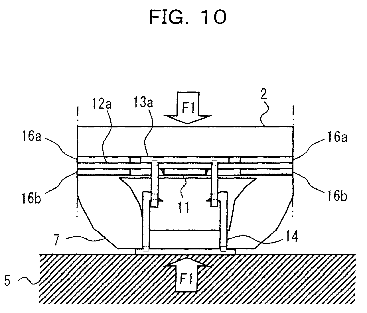
- FIG. 10 is a sectional view illustrating an example of a second state of the RFID tag 1a as seen from the front.
- the second state is where the attaching band 2 is fastened by an operator so that the RFID tag 1 a is attached to the object of attachment 5.
- the attaching band 2 is pressed against the object of attachment 5, so that the RFID tag 1a undergoes pressing force F1 that presses the base 21 toward the base 23 as well as the base 23 toward the base 21.
- the pressing force F1 compresses the spacer 7 for elastic deformation, whereby the hooks 22 and the hooks 24 are locked on each other.
- FIG. 11 is a sectional view illustrating an example of a third state of the RFID tag 1a as seen from the front.
- the third state is where the RFID tag 1a attached is detached from the object of attachment 5.
- the spacer 7 produces elastic restoring force (reactive force) F2 against the pressing force F1.
- the RFID tag 1a is subjected to the elastic restoring force F2 which presses both end portions of the inlet substrate 12a upward and the base 23 downward.
- the distance between the center portion of the inlet substrate 12a and the base 23 is maintained because the bases 21 and 23 are constrained with the hooks 22 and 24 locked on each other.
- the center portion and both end portions of the inlet substrate 12a undergo the forces in the opposite directions, which destroy the inlet substrate 12a and the antenna pattern 17.
- the elastic restoring force F2 exceeds the strength of the inlet substrate 12a.
- FIG. 12 is a bottom view illustrating an example of a first step in the method of manufacturing the RFID tag 1a.
- FIG. 13 is a side view illustrating the example of the first step in the method of manufacturing the RFID tag 1 a.
- holes 31, 32, 33, and 34 are formed through the center portion of the inlet substrate 12a.
- the chip 11 is mounted on the bottom surface of the center portion of the inlet substrate 12a.
- FIG. 14 is a bottom view illustrating an example of a second step in the method of manufacturing the RFID tag 1a.
- FIG. 15 is a side view illustrating the example of the second step in the method of manufacturing the RFID tag 1a.
- the base 21 is arranged on the top surface of the center portion of the inlet substrate 12a.
- FIG. 16 is a bottom view illustrating an example of a third step in the method of manufacturing the RFID tag 1a.
- FIG. 17 is a side view illustrating the example of the third step in the method of manufacturing the RFID tag 1a.
- the hooks 22 are arranged on the bottom surface of the center portion of the inlet substrate 12a.
- the base 21 and the hooks 22 are joined to each other.
- FIG. 18 is a bottom view illustrating an example of a fourth step in the method of manufacturing the RFID tag 1a.
- FIG. 19 is a side view illustrating the example of the fourth step in the method of manufacturing the RFID tag 1a.
- the attaching band 2 is arranged on the top surface of the inlet substrate 12a. The top surfaces of both end portions of the inlet substrate 12a are bonded to the bottom surface of the attaching band 2 by the adhesive agent 16a. The base 21 and the attaching band 2 are not bonded to each other.
- FIG. 20 is a sectional view illustrating an example of a fifth step in the method of manufacturing the RFID tag 1a.
- the spacer 7 with the destruction mechanism 14 on its bottom wall is arranged on the bottom surface of the inlet substrate 12a.
- the bottom surfaces of both end portions of the inlet substrate 12a are bonded to the top surface of the top wall of the spacer 7 by the adhesive agent 16b.
- the inlet substrate 12a is destroyed when the RFID tag 1a attached to the object of attachment 5 is detached. This makes it possible to prevent the unauthorized use of the RFID tag 1a.
- FIG. 21 is a sectional view illustrating an example of the RFID tag 1a with malfunction preventive measures as seen from the front.
- a stopper 26 is put on the hooks 22 to stop the hook holes 25 after manufacturing until attachment so that the hooks 22 and 24 will not lock into each other due to a shock or impact during shipment. The stopper 26 is removed immediately before attachment.
- the stopper 26 may be put on the hooks 24.
- the stoppers 26 may be put on both the hooks 22 and 24.
- FIG. 22 is a bottom view illustrating an example of the configuration of the RFID tag 1b.
- the components of the RFID tag 1b identical or equivalent to those of the RFID tag 1 a will be designated by the same reference numerals as those of the RFID tag 1a. Description thereof will be omitted here.
- the RFID tag 1 b has an inlet substrate 12b instead of the inlet substrate 12a.
- FIG. 23 is a bottom view illustrating an example of the configuration of the inlet substrate 12b.
- the inlet substrate 12b has four notches (grooves) 41 at the borders between the center portion and both end portions.
- the notches 41 are intended to lower the strength of the borders.
- the RFID tag 1b reaches the third state through the first and second states as in Embodiment 1, the notches 41 increase the certainty of destruction of the inlet substrate 12b.
- the notches 41 are formed in the long sides of the plane of the inlet substrate 12b so as to extend in the direction of the borders.
- grooves may be formed in the surface of the inlet substrate along the borders so that the grooves ensure the destruction.
- the grooves may be formed in either of the top and bottom surfaces.
- the notches 41 in the long sides of the plane of the inlet substrate and the grooves in the surface of the inlet substrate may be used in combination.
- the inlet substrate 12b is destroyed with higher reliability when the RFID tag 1b attached to the object of attachment 5 is detached.
- FIG. 24 is a sectional view illustrating an example of the third state of the RFID tag 1c as seen from the front.
- the diagram depicts the third state that is reached through the first and second states as in Embodiment 1, i.e., where the RFID tag 1c is detached from the object of attachment 5.
- the components of the RFID tag 1 c identical or equivalent to those of the RFID tag 1 a will be designated by the same reference numerals as those of the RFID tag 1a. Description thereof will be omitted here.
- the RFID tag 1c has a destruction mechanism 13b instead of the destruction mechanism 13a.
- FIG. 25 is a front view illustrating an example of the configuration of the destruction mechanism 13b.
- the components of the destruction mechanism 13b identical or equivalent to those of the destruction mechanism 13a will be designated by the same reference numerals as those of the destruction mechanism 13a. Description thereof will be omitted here.
- the destruction mechanism 13b has wires 42 instead of the hooks 22.
- FIG. 26 is a perspective view illustrating an example of the configuration of the destruction mechanism 13b and the inlet substrate 12a.
- the point of view in the diagram is located at the bottom side of the inlet substrate 12a.
- FIG. 27 is a sectional view illustrating an example of the second state of the RFID tag 1d as seen from the front.
- the diagram depicts the same second state as in Embodiment 1, i.e., where the RFID tag 1d is attached to the object of attachment 5.
- the components of the RFID tag 1d identical or equivalent to those of the RFID tag 1a will be designated by the same reference numerals as those of the RFID tag 1a. Description thereof will be omitted here.
- the RFID tag 1 d has a destruction mechanism 13c instead of the destruction mechanism 13a.
- FIG. 28 is a front view illustrating an example of the configuration of the destruction mechanism 13c.
- the components of the destruction mechanism 13c identical or equivalent to those of the destruction mechanism 13a will be designated by the same reference numerals as those of the destruction mechanism 13a. Description thereof will be omitted here.
- the destruction mechanism 13c has an additional protrusion 43 on the bottom surface of the base 21.
- the protrusion 43 is positioned so as to be opposed to the center portion of the chip 11 across the inlet substrate 12a.
- the top of the protrusion 43 is directed toward the inlet substrate 12a.
- FIG. 29 is a sectional view illustrating an example of the third state of the RFID tag 1d as seen from the front.
- the diagram depicts the same third state as in Embodiment 1, i.e., where the RFID tag 1d is detached from the object of attachment 5.
- the chip 11 and the inlet substrate 12a are destroyed when the RFID tag 1d attached to the object of attachment 5 is detached. This makes it possible to prevent the unauthorized use of the RFID tag 1d and the chip 11.
- the first locking section corresponds to the hooks 22 or the wires 42.
- the second locking section corresponds to the destruction mechanism 14.
- the destruction section corresponds to the base 21 or the protrusion 43.
- the support section corresponds to the inlet substrate 12a or the inlet substrate 12b.
- the RFID tags disclosed in the foregoing respective embodiments are destroyed when detached from the object of attachment.
Landscapes
- Engineering & Computer Science (AREA)
- Physics & Mathematics (AREA)
- General Physics & Mathematics (AREA)
- Theoretical Computer Science (AREA)
- Computer Hardware Design (AREA)
- Microelectronics & Electronic Packaging (AREA)
- Computer Security & Cryptography (AREA)
- General Engineering & Computer Science (AREA)
- Burglar Alarm Systems (AREA)
- Details Of Aerials (AREA)
- Credit Cards Or The Like (AREA)
Abstract
An RFID tag has an IC chip (11) and an antenna connected to the IC chip, the RFID tag including: a spacer (7) that has elasticity; a first locking section (13a) that is formed around the IC chip; a second locking section (14) that is arranged in a position apart from the first locking section across the spacer, is displaced toward the first locking section and locked on the first locking section by pressing force (F1) with which the spacer is pressed, and applies reactive force (F2) against the pressing force around the IC chip via the first locking section when the pressing force is removed; and a destruction section that destroys the IC chip or the antenna with the reactive force from the second locking section.

Description
- The present invention relates to a radio frequency identification (RFID) tag which has an IC chip and an antenna connected to the integrated circuit (IC) chip.
- In order to prevent the unauthorized use of RFID tag, technologies are known in which an RFID tag, once attached to an intended article, is destroyed by the removal of only an upper part of the RFID tag.
- [Patent Document 1] Japanese Laid-Open Patent Publication No.
2000-48147 - [Patent Document 2] Japanese Laid-Open Patent Publication No.
2005-242971 - [Patent Document 3] Japanese Patent No.
3,636,202 - The foregoing RFID tag for preventing unauthorized use needs to be bonded to an intended article. The RFID tag is therefore not applicable to one that is not bonded to the intended articles. Moreover, the RFID tag for preventing unauthorized use becomes ineffective if the RFID tag is taken off from the intended article.
- The present invention has been achieved in view of the foregoing problems. It is desirable to provide an RFID tag which, once attached to an object of attachment, is to be destroyed when detached from the object of attachment.
- According to embodiments of an aspect of the invention, an RFID tag has an IC chip and an antenna connected to the IC chip, the RFID tag including: a spacer that has elasticity; a first locking section that is formed around the IC chip; a second locking section that is arranged in a position apart from the first locking section across the spacer, is displaced toward the first locking section and locked on the first locking section by pressing force with which the spacer is pressed, and applies reactive force against the pressing force around the IC chip via the first locking section when the pressing force is removed; and a destruction section that destroys the IC chip or the antenna with the reactive force from the second locking section.
- Preferred features of the present invention will now be described, purely by way of example, with reference to the accompanying drawings, in which:
-
-
FIG. 1 is a bottom view illustrating an example of the configuration of an RFID tag 1a; -
FIG. 2 is a front view illustrating the example of the configuration of the RFID tag 1 a; -
FIG. 3 is a top view illustrating an example of the state of attachment of the RFID tag 1a; -
FIG. 4 is a front view illustrating the example of the state of attachment of the RFID tag 1a; -
FIG. 5 is a sectional view illustrating an example of the configuration of the RFID tag 1a as seen from the front; -
FIG. 6 is a front view illustrating an example of the configuration ofdestruction mechanisms -
FIG. 7 is a bottom view illustrating an example of the configuration in the vicinity of thedestruction mechanism 13a; -
FIG. 8 is a side view illustrating the example of the configuration in the vicinity of thedestruction mechanism 13a; -
FIG. 9 is a sectional view illustrating an example of a first state of the RFID tag 1 a as seen from the front; -
FIG. 10 is a sectional view illustrating an example of a second state of the RFID tag 1a as seen from the front; -
FIG. 11 is a sectional view illustrating an example of a third state of the RFID tag 1 a as seen from the front; -
FIG. 12 is a bottom view illustrating an example of a first step in the method of manufacturing the RFID tag 1a; -
FIG. 13 is a side view illustrating the example of the first step in the method of manufacturing the RFID tag 1a; -
FIG. 14 is a bottom view illustrating an example of a second step in the method of manufacturing the RFID tag 1a; -
FIG. 15 is a side view illustrating the example of the second step in the method of manufacturing the RFID tag 1a; -
FIG. 16 is a bottom view illustrating an example of a third step in the method of manufacturing the RFID tag 1a; -
FIG. 17 is a side view illustrating the example of the third step in the method of manufacturing the RFID tag 1a; -
FIG. 18 is a bottom view illustrating an example of a fourth step in the method of manufacturing the RFID tag 1a; -
FIG. 19 is a side view illustrating the example of the fourth step in the method of manufacturing the RFID tag 1a; -
FIG. 20 is a sectional view illustrating an example of a fifth step in the method of manufacturing the RFID tag 1a; -
FIG. 21 is a sectional view illustrating an example of the RFID tag 1a with malfunction preventive measures as seen from the front; -
FIG. 22 is a bottom view illustrating an example of the configuration of an RFID tag 1b; -
FIG. 23 is a bottom view illustrating an example of the configuration of an inlet substrate 12b; -
FIG. 24 is a sectional view illustrating an example of the third state of the RFID tag 1 c as seen from the front; -
FIG. 25 is a front view illustrating an example of the configuration of adestruction mechanism 13b; -
FIG. 26 is a perspective view illustrating an example of the configuration of thedestruction mechanism 13b and theinlet substrate 12a; -
FIG. 27 is a sectional view illustrating an example of the second state of an RFID tag 1d as seen from the front; -
FIG. 28 is a front view illustrating an example of the configuration of adestruction mechanism 13c; and -
FIG. 29 is a sectional view illustrating an example of the third state of the RFID tag 1 d as seen from the front. - Hereinafter, embodiments of the present invention will be described with reference to the drawings.
- The configuration of an RFID tag 1 a according to the present embodiment will be described below.
-
FIG. 1 is a bottom view illustrating an example of the configuration of the RFID tag 1a.FIG. 2 is a front view illustrating the example of the configuration of the RFID tag 1a. The RFID tag 1a of the present embodiment includes an attachingband 2, acircuit accommodating section 3, andspacers 6. The attachingband 2 has two ends that can be connected to each other, with the same function as that of a cable tie. Thecircuit accommodating section 3 has walls which constitute aspacer 7. -
FIG. 3 is a top view illustrating an example of the state of attachment of the RFID tag 1a.FIG. 4 is a front view illustrating the example of the state of attachment of the RFID tag 1a. The RFID tag 1a is attached to an object ofattachment 5. Here, the attachingband 2 is wound around and fastened to the object ofattachment 5, whereby thecircuit accommodating section 3 and thespacers 6 are compressed. -
FIG. 5 is a sectional view illustrating an example of the configuration of the RFID tag 1a as seen from the front. The diagram depicts the interior of thecircuit accommodating section 3 of the RFID tag 1a. Thecircuit accommodating section 3 includes a chip 11 (IC chip), aninlet substrate 12a,destruction mechanisms spacer 7, andadhesive agents spacer 7, the upper wall surface in contact with theinlet substrate 12a will be referred to as a top wall, the lower wall surface to be bonded to thedestruction mechanism 14 as a bottom wall, and the remaining wall surfaces as side walls. Thespacers spacers - The area of the
inlet substrate 12a in contact with thedestruction mechanism 13a will be referred to as a center portion (first location). The areas to be bonded to the attachingband 2 will be referred to as end portions (second location). The top surface of thechip 11 is bonded to the bottom surface of the center portion of theinlet substrate 12a. Thechip 11 has electrodes which are connected to an antenna pattern on theinlet substrate 12a. The bottom surfaces of both end portions of theinlet substrate 12a are bonded to the top surface of the top wall of thespacer 7 by theadhesive agent 16b. The top surfaces of both end portions of theinlet substrate 12a are bonded to the bottom surface of the attachingband 2 by theadhesive agent 16a. -
FIG. 6 is a front view illustrating an example of the configuration of thedestruction mechanisms destruction mechanism 13a, and the lower thedestruction mechanism 14. - The
destruction mechanism 13a has abase 21 and hooks 22. Thebase 21 and thehooks 22 are joined to each other. Thebase 21 is fixed to the top surface of the center portion of theinlet substrate 12a. Thehooks 22 are extended through theinlet substrate 12a into the internal space of thespacer 7. Thedestruction mechanism 13a is not joined to the attachingband 2. - The
destruction mechanism 14 has abase 23 and hooks 24. Thebase 23 and thehooks 24 are joined to each other. Thebase 23 is fixed to the bottom surface of the bottom wall of thespacer 7. Thehooks 24 are extended through the bottom wall of thespacer 7 into the internal space of thespacer 7. - The
hooks 22 havehook holes 25 for the protrusions of thehooks 24 to catch in. -
FIG. 7 is a bottom view illustrating an example of the configuration in the vicinity of thedestruction mechanism 13a. The diagram depicts the attachingband 2, thedestruction mechanism 13a, theinlet substrate 12a, and thechip 11 of the RFID tag 1a.FIG. 8 is a side view illustrating the example of the configuration in the vicinity of thedestruction mechanism 13a. This diagram is a side view taken from the right ofFIG. 7 . The left of the diagram corresponds to below theinlet substrate 12a. Theinlet substrate 12a has an antenna pattern 17 (antenna). - Hereinafter, description will be given of a change in the state of the RFID tag 1 a when attached.
-
FIG. 9 is a sectional view illustrating an example of a first state of the RFID tag 1 a as seen from the front. The first state refers to where the RFID tag 1 a is yet to be attached to the object ofattachment 5, and the bottom surface of the bottom wall of thespacer 7 is in contact with the object ofattachment 5. -
FIG. 10 is a sectional view illustrating an example of a second state of the RFID tag 1a as seen from the front. The second state is where the attachingband 2 is fastened by an operator so that the RFID tag 1 a is attached to the object ofattachment 5. When fastened, the attachingband 2 is pressed against the object ofattachment 5, so that the RFID tag 1a undergoes pressing force F1 that presses the base 21 toward the base 23 as well as the base 23 toward thebase 21. The pressing force F1 compresses thespacer 7 for elastic deformation, whereby thehooks 22 and thehooks 24 are locked on each other. - Hereinafter, description will be given of a change in the state of the RFID tag 1 a when detached.
-
FIG. 11 is a sectional view illustrating an example of a third state of the RFID tag 1a as seen from the front. The third state is where the RFID tag 1a attached is detached from the object ofattachment 5. Thespacer 7 produces elastic restoring force (reactive force) F2 against the pressing force F1. - When the attaching
band 2 is cut or otherwise loosened and the fastening force of the attachingband 2 decreases to reduce the pressing force F1, the RFID tag 1a is subjected to the elastic restoring force F2 which presses both end portions of theinlet substrate 12a upward and the base 23 downward. In the meantime, the distance between the center portion of theinlet substrate 12a and thebase 23 is maintained because thebases hooks inlet substrate 12a undergo the forces in the opposite directions, which destroy theinlet substrate 12a and theantenna pattern 17. - The elastic restoring force F2 exceeds the strength of the
inlet substrate 12a. - Since the
destruction mechanisms spacer 7, an operator who detaches the RFID tag 1 a from the object ofattachment 5 in an unauthorized fashion is not able to learn of thedestruction mechanisms - Description will now be given of the method of manufacturing the RFID tag 1 a.
-
FIG. 12 is a bottom view illustrating an example of a first step in the method of manufacturing the RFID tag 1a.FIG. 13 is a side view illustrating the example of the first step in the method of manufacturing the RFID tag 1 a. In the first step, holes 31, 32, 33, and 34 are formed through the center portion of theinlet substrate 12a. Thechip 11 is mounted on the bottom surface of the center portion of theinlet substrate 12a. -
FIG. 14 is a bottom view illustrating an example of a second step in the method of manufacturing the RFID tag 1a.FIG. 15 is a side view illustrating the example of the second step in the method of manufacturing the RFID tag 1a. Thebase 21 is arranged on the top surface of the center portion of theinlet substrate 12a. -
FIG. 16 is a bottom view illustrating an example of a third step in the method of manufacturing the RFID tag 1a.FIG. 17 is a side view illustrating the example of the third step in the method of manufacturing the RFID tag 1a. Thehooks 22 are arranged on the bottom surface of the center portion of theinlet substrate 12a. Thebase 21 and thehooks 22 are joined to each other. -
FIG. 18 is a bottom view illustrating an example of a fourth step in the method of manufacturing the RFID tag 1a.FIG. 19 is a side view illustrating the example of the fourth step in the method of manufacturing the RFID tag 1a. The attachingband 2 is arranged on the top surface of theinlet substrate 12a. The top surfaces of both end portions of theinlet substrate 12a are bonded to the bottom surface of the attachingband 2 by theadhesive agent 16a. Thebase 21 and the attachingband 2 are not bonded to each other. -
FIG. 20 is a sectional view illustrating an example of a fifth step in the method of manufacturing the RFID tag 1a. Thespacer 7 with thedestruction mechanism 14 on its bottom wall is arranged on the bottom surface of theinlet substrate 12a. The bottom surfaces of both end portions of theinlet substrate 12a are bonded to the top surface of the top wall of thespacer 7 by theadhesive agent 16b. - According to the present embodiment, the
inlet substrate 12a is destroyed when the RFID tag 1a attached to the object ofattachment 5 is detached. This makes it possible to prevent the unauthorized use of the RFID tag 1a. - Measures for preventing malfunction of the RFID tag 1 a will be described below.
-
FIG. 21 is a sectional view illustrating an example of the RFID tag 1a with malfunction preventive measures as seen from the front. Astopper 26 is put on thehooks 22 to stop the hook holes 25 after manufacturing until attachment so that thehooks stopper 26 is removed immediately before attachment. - Alternatively, the
stopper 26 may be put on thehooks 24. Thestoppers 26 may be put on both thehooks - Hereinafter, description will be given of the configuration of an RFID tag 1 b according to the present embodiment.
-
FIG. 22 is a bottom view illustrating an example of the configuration of the RFID tag 1b. The components of the RFID tag 1b identical or equivalent to those of the RFID tag 1 a will be designated by the same reference numerals as those of the RFID tag 1a. Description thereof will be omitted here. As compared to the RFID tag 1a, the RFID tag 1 b has an inlet substrate 12b instead of theinlet substrate 12a. -
FIG. 23 is a bottom view illustrating an example of the configuration of the inlet substrate 12b. As compared to theinlet substrate 12a, the inlet substrate 12b has four notches (grooves) 41 at the borders between the center portion and both end portions. Thenotches 41 are intended to lower the strength of the borders. When the RFID tag 1b reaches the third state through the first and second states as inEmbodiment 1, thenotches 41 increase the certainty of destruction of the inlet substrate 12b. Thenotches 41 are formed in the long sides of the plane of the inlet substrate 12b so as to extend in the direction of the borders. - Alternatively, grooves may be formed in the surface of the inlet substrate along the borders so that the grooves ensure the destruction. The grooves may be formed in either of the top and bottom surfaces. The
notches 41 in the long sides of the plane of the inlet substrate and the grooves in the surface of the inlet substrate may be used in combination. - According to the present embodiment, the inlet substrate 12b is destroyed with higher reliability when the RFID tag 1b attached to the object of
attachment 5 is detached. - Now, description will be given of the configuration of an RFID tag 1c according to the present embodiment.
-
FIG. 24 is a sectional view illustrating an example of the third state of the RFID tag 1c as seen from the front. The diagram depicts the third state that is reached through the first and second states as inEmbodiment 1, i.e., where the RFID tag 1c is detached from the object ofattachment 5. The components of the RFID tag 1 c identical or equivalent to those of the RFID tag 1 a will be designated by the same reference numerals as those of the RFID tag 1a. Description thereof will be omitted here. As compared to the RFID tag 1a, the RFID tag 1c has adestruction mechanism 13b instead of thedestruction mechanism 13a. -
FIG. 25 is a front view illustrating an example of the configuration of thedestruction mechanism 13b. The components of thedestruction mechanism 13b identical or equivalent to those of thedestruction mechanism 13a will be designated by the same reference numerals as those of thedestruction mechanism 13a.
Description thereof will be omitted here. As compared to thedestruction mechanism 13a, thedestruction mechanism 13b haswires 42 instead of thehooks 22. -
FIG. 26 is a perspective view illustrating an example of the configuration of thedestruction mechanism 13b and theinlet substrate 12a. The point of view in the diagram is located at the bottom side of theinlet substrate 12a. When the RFID tag 1 c is attached, thewires 42 are caught on thehooks 24 as if thehooks 22 are in the second state ofEmbodiment 1. Thebases bases inlet substrates 12a undergo forces in the respective opposite directions as in the third state ofEmbodiment 1. Theinlet substrate 12a is thus destroyed. - Now, description will be given of the configuration of an RFID tag 1d according to the present embodiment.
-
FIG. 27 is a sectional view illustrating an example of the second state of the RFID tag 1d as seen from the front. The diagram depicts the same second state as inEmbodiment 1, i.e., where the RFID tag 1d is attached to the object ofattachment 5. The components of the RFID tag 1d identical or equivalent to those of the RFID tag 1a will be designated by the same reference numerals as those of the RFID tag 1a. Description thereof will be omitted here. As compared to the RFID tag 1a, the RFID tag 1 d has adestruction mechanism 13c instead of thedestruction mechanism 13a. -
FIG. 28 is a front view illustrating an example of the configuration of thedestruction mechanism 13c. The components of thedestruction mechanism 13c identical or equivalent to those of thedestruction mechanism 13a will be designated by the same reference numerals as those of thedestruction mechanism 13a.
Description thereof will be omitted here. As compared to thedestruction mechanism 13a, thedestruction mechanism 13c has anadditional protrusion 43 on the bottom surface of thebase 21. Theprotrusion 43 is positioned so as to be opposed to the center portion of thechip 11 across theinlet substrate 12a. The top of theprotrusion 43 is directed toward theinlet substrate 12a. -
FIG. 29 is a sectional view illustrating an example of the third state of the RFID tag 1d as seen from the front. The diagram depicts the same third state as inEmbodiment 1, i.e., where the RFID tag 1d is detached from the object ofattachment 5. - When the attaching
band 2 is loosened to reduce the pressing force F1 as in the third state ofEmbodiment 1, the elastic restoring force F2 from thespacer 7, which presses both end portions of theinlet substrate 12a upward and the base 23 downward, exceeds the pressing force F1. In the meantime, the distance between theprotrusion 43 and thebase 23 is maintained because thebases hooks protrusion 43 and theinlet substrate 12a undergo forces in the opposite directions, so that the top of theprotrusion 43 sticks into theinlet substrate 12a to destroy thechip 11 and theinlet substrate 12a. - According to the present embodiment, the
chip 11 and theinlet substrate 12a are destroyed when the RFID tag 1d attached to the object ofattachment 5 is detached. This makes it possible to prevent the unauthorized use of the RFID tag 1d and thechip 11. - The first locking section corresponds to the
hooks 22 or thewires 42. The second locking section corresponds to thedestruction mechanism 14. The destruction section corresponds to the base 21 or theprotrusion 43. The support section corresponds to theinlet substrate 12a or the inlet substrate 12b. - Once attached to an object of attachment, the RFID tags disclosed in the foregoing respective embodiments are destroyed when detached from the object of attachment.
- All examples and conditional language recited herein are intended for pedagogical purposes to aid the reader in understanding the invention and the concepts contributed by the inventor to furthering the art, and are to be construed as being without limitation to such specifically recited examples and conditions, nor does the organization of such examples in the specification relate to a depicting of the superiority and inferiority of embodiments of the invention. Although the embodiment(s) of the present inventions have been described in detail, it should be understood that the various changes, substitutions, and alterations could be made hereto without departing from the scope of the invention.
Claims (11)
- An RFID tag having an IC chip and an antenna connected to the IC chip, the RFID tag comprising:a spacer that has elasticity;a first locking section that is formed around the IC chip;a second locking section that is arranged in a position apart from the first locking section across the spacer, is displaced toward the first locking section and locked on the first locking section by pressing force with which the spacer is pressed, and applies reactive force against the pressing force around the IC chip via the first locking section when the pressing force is removed; anda destruction section that destroys the IC chip or the antenna with the reactive force from the second locking section.
- The RFID tag according to claim 1, further comprisinga band for attaching the RFID tag to an object of attachment, andthe band produces the pressing force when fastened to the object of attachment.
- The RFID tag according to claim 1 or 2, further comprisinga support section that supports the antenna and is to be destroyed with the antenna by the destruction section.
- The RFID tag according to claim 3, whereinthe support section has a groove that helps the destroying of the destruction section.
- The RFID tag according to any of claims 1 to 4, whereinthe destruction section has a protrusion toward the IC chip, andthe protrusion is to be brought into contact with the IC chip to destroy the IC chip by the reactive force.
- The RFID tag according to any of claims 1 to 5, whereinthe reactive force is an elastic restoring force of the spacer.
- The RFID tag according to any of claims 1 to 6, whereinthe destruction section is arranged on a side opposite from the second locking section across the spacer.
- The RFID tag according to any of claims 1 to 7, whereinthe destruction section is fixed to the first locking section.
- The RFID tag according to any of claims 1 to 8, whereinthe spacer, the first locking section, and the second locking section are arranged on a side of the antenna opposite from the destruction section.
- The RFID tag according to any of claims 1 to 9, whereinthe destruction section is in contact with a first location of the antenna or the IC chip,the spacer is in contact with a second location of the antenna or the IC chip,
andthe reactive force displaces the first location and the second location in opposite directions. - The RFID tag according to any of claims 1 to 10, further comprising a stopper that is formed on at least either one of the first locking section and the second locking section to prevent locking between the first locking section and the second locking section, wherein
the stopper is removed before the RFID tag is attached to the object of attachment.
Applications Claiming Priority (1)
| Application Number | Priority Date | Filing Date | Title |
|---|---|---|---|
| JP2009040269A JP5220654B2 (en) | 2009-02-24 | 2009-02-24 | RFID tag |
Publications (1)
| Publication Number | Publication Date |
|---|---|
| EP2221754A1 true EP2221754A1 (en) | 2010-08-25 |
Family
ID=42133773
Family Applications (1)
| Application Number | Title | Priority Date | Filing Date |
|---|---|---|---|
| EP20100152276 Withdrawn EP2221754A1 (en) | 2009-02-24 | 2010-02-01 | RFID tag |
Country Status (5)
| Country | Link |
|---|---|
| US (1) | US8242916B2 (en) |
| EP (1) | EP2221754A1 (en) |
| JP (1) | JP5220654B2 (en) |
| KR (1) | KR101050439B1 (en) |
| CN (1) | CN101814155B (en) |
Cited By (2)
| Publication number | Priority date | Publication date | Assignee | Title |
|---|---|---|---|---|
| WO2018193309A1 (en) * | 2017-04-21 | 2018-10-25 | Assa Abloy Ab | Housing for identification device |
| FR3106425A1 (en) * | 2020-01-20 | 2021-07-23 | Safran Aircraft Engines | Radio frequency label comprising a means of destruction and associated method |
Families Citing this family (2)
| Publication number | Priority date | Publication date | Assignee | Title |
|---|---|---|---|---|
| WO2012066463A1 (en) * | 2010-11-15 | 2012-05-24 | Orpak Systems Ltd. | Device for automated fuel delivery authorization and method for installation thereof |
| EP3217326B1 (en) | 2016-03-10 | 2019-10-23 | Assa Abloy AB | Tamper resistant tag |
Citations (6)
| Publication number | Priority date | Publication date | Assignee | Title |
|---|---|---|---|---|
| JP2000048147A (en) | 1998-07-27 | 2000-02-18 | Toshiba Chem Corp | Label-like noncontact data carrier and its manufacture |
| JP3636202B2 (en) | 2003-05-26 | 2005-04-06 | オムロン株式会社 | Information carrier, information recording medium, sensor, article management method |
| JP2005242971A (en) | 2004-01-26 | 2005-09-08 | Toppan Forms Co Ltd | Thread, manufacturing method thereof, and sheet |
| WO2006074518A1 (en) * | 2005-01-14 | 2006-07-20 | Matthew Henderson | A transponder bolt seal and a housing for a transponder |
| WO2007121508A1 (en) * | 2006-04-21 | 2007-11-01 | Richard Ruggiero | Spring-loaded, circuit-breaking, security seal |
| US20080266108A1 (en) * | 2006-12-19 | 2008-10-30 | Charles Michael Teeter | Disposable and tamper-resistant rfid lock |
Family Cites Families (5)
| Publication number | Priority date | Publication date | Assignee | Title |
|---|---|---|---|---|
| JP2002063559A (en) * | 2000-08-23 | 2002-02-28 | Seiko Precision Inc | Data carrier device and management system |
| JP4342771B2 (en) * | 2002-05-15 | 2009-10-14 | リンテック株式会社 | IC tag |
| JP2006012138A (en) * | 2004-05-31 | 2006-01-12 | Lien-Feng Lin | Electronic seal |
| CN1938717B (en) * | 2004-07-08 | 2010-12-08 | Ykk株式会社 | Fastening products with wireless IC tags |
| WO2006055774A1 (en) * | 2004-11-17 | 2006-05-26 | Sensormatic Electronics Corporation | Magnetically releasable electronic article surveillance tag |
-
2009
- 2009-02-24 JP JP2009040269A patent/JP5220654B2/en not_active Expired - Fee Related
-
2010
- 2010-01-27 US US12/694,755 patent/US8242916B2/en not_active Expired - Fee Related
- 2010-02-01 EP EP20100152276 patent/EP2221754A1/en not_active Withdrawn
- 2010-02-05 KR KR1020100011007A patent/KR101050439B1/en not_active Expired - Fee Related
- 2010-02-22 CN CN2010101213327A patent/CN101814155B/en not_active Expired - Fee Related
Patent Citations (6)
| Publication number | Priority date | Publication date | Assignee | Title |
|---|---|---|---|---|
| JP2000048147A (en) | 1998-07-27 | 2000-02-18 | Toshiba Chem Corp | Label-like noncontact data carrier and its manufacture |
| JP3636202B2 (en) | 2003-05-26 | 2005-04-06 | オムロン株式会社 | Information carrier, information recording medium, sensor, article management method |
| JP2005242971A (en) | 2004-01-26 | 2005-09-08 | Toppan Forms Co Ltd | Thread, manufacturing method thereof, and sheet |
| WO2006074518A1 (en) * | 2005-01-14 | 2006-07-20 | Matthew Henderson | A transponder bolt seal and a housing for a transponder |
| WO2007121508A1 (en) * | 2006-04-21 | 2007-11-01 | Richard Ruggiero | Spring-loaded, circuit-breaking, security seal |
| US20080266108A1 (en) * | 2006-12-19 | 2008-10-30 | Charles Michael Teeter | Disposable and tamper-resistant rfid lock |
Cited By (3)
| Publication number | Priority date | Publication date | Assignee | Title |
|---|---|---|---|---|
| WO2018193309A1 (en) * | 2017-04-21 | 2018-10-25 | Assa Abloy Ab | Housing for identification device |
| US11030511B2 (en) | 2017-04-21 | 2021-06-08 | Assaabloy Ab | Housing for identification device |
| FR3106425A1 (en) * | 2020-01-20 | 2021-07-23 | Safran Aircraft Engines | Radio frequency label comprising a means of destruction and associated method |
Also Published As
| Publication number | Publication date |
|---|---|
| CN101814155B (en) | 2013-01-09 |
| JP5220654B2 (en) | 2013-06-26 |
| KR101050439B1 (en) | 2011-07-19 |
| US8242916B2 (en) | 2012-08-14 |
| JP2010198154A (en) | 2010-09-09 |
| US20100214101A1 (en) | 2010-08-26 |
| KR20100097014A (en) | 2010-09-02 |
| CN101814155A (en) | 2010-08-25 |
Similar Documents
| Publication | Publication Date | Title |
|---|---|---|
| KR102162631B1 (en) | Permanent Attached On Surface Tire UHF Band RFID Tag And Their Manufacturing Methods | |
| US8242916B2 (en) | RFID tag | |
| EP2374095B1 (en) | Radio frequency identification tag | |
| EP1958171A2 (en) | Tuned radio frequency identification (rfid) circuit used as a security device for wristbands and package security | |
| EP2696311B1 (en) | Rfid tag | |
| US10719756B2 (en) | UHF band RFID tag and UHF band RFID tagged article | |
| EP2813975B1 (en) | Ic tag | |
| EP3732748B1 (en) | Rfid tags using multi-layer constructions for improved durability | |
| JP2009116649A (en) | RFID tag | |
| CN117015354A (en) | Torsion protection shell of glass tag transponder | |
| JP4382783B2 (en) | RFID tag | |
| EP1962230A1 (en) | RFID tag | |
| KR100567840B1 (en) | Radio frequency identification tag for metal with heat resistance and its manufacturing method | |
| US9798970B2 (en) | Radio frequency identification tag | |
| KR101210399B1 (en) | Rfid tag including fastening means for antenna and the manufacturing method of the same | |
| JP6232847B2 (en) | RFID tag | |
| KR101113851B1 (en) | RFID tag | |
| KR20060119635A (en) | RFID tag | |
| JP2009054088A (en) | Reinforcing member | |
| EP3561731A1 (en) | Rfid tag | |
| JP5006916B2 (en) | RFID tag | |
| JP2016090867A (en) | Sealing tool | |
| KR100967092B1 (en) | A fixing device for rfid tags | |
| KR101038498B1 (en) | RFID tag and its manufacturing method | |
| KR100719973B1 (en) | Radio Frequency Identification Tag with Connection Protection |
Legal Events
| Date | Code | Title | Description |
|---|---|---|---|
| PUAI | Public reference made under article 153(3) epc to a published international application that has entered the european phase |
Free format text: ORIGINAL CODE: 0009012 |
|
| AK | Designated contracting states |
Kind code of ref document: A1 Designated state(s): AT BE BG CH CY CZ DE DK EE ES FI FR GB GR HR HU IE IS IT LI LT LU LV MC MK MT NL NO PL PT RO SE SI SK SM TR |
|
| AX | Request for extension of the european patent |
Extension state: AL BA RS |
|
| 17P | Request for examination filed |
Effective date: 20110112 |
|
| STAA | Information on the status of an ep patent application or granted ep patent |
Free format text: STATUS: THE APPLICATION HAS BEEN WITHDRAWN |
|
| 18W | Application withdrawn |
Effective date: 20140219 |