EP2219217A2 - Halbleitermodul - Google Patents
Halbleitermodul Download PDFInfo
- Publication number
- EP2219217A2 EP2219217A2 EP20090016025 EP09016025A EP2219217A2 EP 2219217 A2 EP2219217 A2 EP 2219217A2 EP 20090016025 EP20090016025 EP 20090016025 EP 09016025 A EP09016025 A EP 09016025A EP 2219217 A2 EP2219217 A2 EP 2219217A2
- Authority
- EP
- European Patent Office
- Prior art keywords
- semiconductor module
- potting compound
- module according
- housing
- preceramic polymer
- Prior art date
- Legal status (The legal status is an assumption and is not a legal conclusion. Google has not performed a legal analysis and makes no representation as to the accuracy of the status listed.)
- Withdrawn
Links
Images

Classifications
-
- H—ELECTRICITY
- H10—SEMICONDUCTOR DEVICES; ELECTRIC SOLID-STATE DEVICES NOT OTHERWISE PROVIDED FOR
- H10W—GENERIC PACKAGES, INTERCONNECTIONS, CONNECTORS OR OTHER CONSTRUCTIONAL DETAILS OF DEVICES COVERED BY CLASS H10
- H10W76/00—Containers; Fillings or auxiliary members therefor; Seals
- H10W76/40—Fillings or auxiliary members in containers, e.g. centering rings
- H10W76/42—Fillings
- H10W76/47—Solid or gel fillings
-
- H—ELECTRICITY
- H10—SEMICONDUCTOR DEVICES; ELECTRIC SOLID-STATE DEVICES NOT OTHERWISE PROVIDED FOR
- H10W—GENERIC PACKAGES, INTERCONNECTIONS, CONNECTORS OR OTHER CONSTRUCTIONAL DETAILS OF DEVICES COVERED BY CLASS H10
- H10W74/00—Encapsulations, e.g. protective coatings
- H10W74/40—Encapsulations, e.g. protective coatings characterised by their materials
- H10W74/47—Encapsulations, e.g. protective coatings characterised by their materials comprising organic materials, e.g. plastics or resins
-
- H—ELECTRICITY
- H10—SEMICONDUCTOR DEVICES; ELECTRIC SOLID-STATE DEVICES NOT OTHERWISE PROVIDED FOR
- H10W—GENERIC PACKAGES, INTERCONNECTIONS, CONNECTORS OR OTHER CONSTRUCTIONAL DETAILS OF DEVICES COVERED BY CLASS H10
- H10W76/00—Containers; Fillings or auxiliary members therefor; Seals
- H10W76/10—Containers or parts thereof
- H10W76/12—Containers or parts thereof characterised by their shape
- H10W76/15—Containers comprising an insulating or insulated base
Definitions
- the invention relates to a semiconductor module according to the preamble of claim 1.
- Such a semiconductor module is for example from the DE 10 2004 021 927 A1 known.
- semiconducting components connected to a substrate are encapsulated with an electrically insulating potting compound. This protects the semiconducting components and their connections from contact with dust or moisture.
- Known potting compounds which are produced for example on the basis of silicone, have a relatively low thermal conductivity ⁇ of 0.2 to 0.3 W / mK. A heat generated during operation of the semiconducting components is relatively poorly dissipated. This limits the performance of the semiconductor module.
- the object of the invention is to eliminate the disadvantages of the prior art.
- a semiconductor module with improved heat dissipation should be specified.
- the power of the semiconductor module is to be increased.
- the potting compound has a matrix formed from a preceramic polymer.
- a potting compound is electrically insulating. It has an excellent thermal conductivity ⁇ .
- One Another advantage of the proposed potting compound is its high temperature resistance. It withstands operating temperatures of up to 300 ° C.
- substrate z. B. understood in the form of a plate present electrically insulating material, which is provided with conductor tracks.
- at least one semiconductive component can be mounted, for example by means of a solder, an adhesive or the like.
- the term "encapsulated” is understood to mean that a semiconducting component previously connected to the substrate is subsequently cast over with the potting compound.
- the potting compound covers the semiconductive device, i. H. surrounds its side walls and its top.
- an underside of the semiconductive component facing the substrate is not or only partially in contact with the potting compound.
- preceramic polymer is understood to mean a polymer which, for. B. passes with increasing temperature, first in a gel-like and subsequently in a thermoset state. In the thermoset state, a preceramic polymer usually has a temperature resistance of up to 300 ° C. With a further increase in temperature, ceramic materials can be produced from preceramic polymers.
- Preceramic polymers include, for example, polysilanes, polycarbosilanes and polyorganosilazanes.
- the preceramic polymer with a degree of filling of up to 80 vol.% Is filled with a filler.
- the thermal conductivity and the viscosity of the preceramic polymer can be increased.
- the filler is a powder formed from a ceramic material having a mean grain size in the range of 0.5 to 500 microns.
- the proposed ceramic material is largely inert. Its addition does not lead to undesired chemical reactions with the preceramic polymer.
- the proposed mean grain size allows casting of the potting compound with conventional devices.
- the thermal conductivity ⁇ of the ceramic material is expediently greater than 10 W / mK, preferably greater than 20 W / mK, at room temperature. Depending on the degree of filling, it is thus possible to increase the thermal conductivity of the preceramic polymer filled with the ceramic material to values above 2 W / mK.
- the proposed potting compound is particularly suitable for the production of a relatively large heat-releasing power semiconductor module during operation.
- the ceramic material is suitably selected from the following group: BN, SiC, Si 3 N 4 , AlN, steatite, cordierite.
- the proposed ceramic materials are characterized by a high thermal conductivity.
- the preceramic polymer is selected from the following group: polysiloxane, polysilazane, polycarbosilane.
- the semiconductor module a semiconducting device is at least partially surrounding housing provided.
- a housing is usually made of a polymer.
- the housing is usually connected to the substrate after the semiconductive device has been mounted thereon.
- an intermediate space between the semiconducting component and a housing surrounding the semiconductive component is at least partially filled with the potting compound.
- the potting compound forms a heat-conducting bridge between the semiconducting component and the housing.
- the potting compound is usually potted in a low-viscosity state. This capillary forces can be exploited and a particularly good thermal contact between the potting compound and the semiconducting device can be ensured.
- the preceramic polymer can be crosslinked to a predetermined degree, for example by increasing the temperature, radiation treatment or the like. The preceramic polymer can then be present in particular in gelatinous or duroplastic form.
- the use of the potting compound according to the invention also allows the omission of the housing commonly used for the production of semiconductor modules.
- a housing surrounding the semiconducting component can be formed in one-piece construction with the potting compound from the preceramic polymer present in thermosetting form.
- the semiconductive device connected to the substrate may e.g. B. are surrounded with a mold, in which then poured the potting compound and then transferred to the thermoset shape.
- the shape may also be a "lost shape", for example a frame placed on the substrate and surrounding the semiconductive component.
- the frame expediently has a matrix formed from the preceramic polymer.
- the preceramic matrix is in duroplastic form.
- the frame has the same material composition as the potting compound.
- the proposed lost form can also be bonded to the substrate before filling the potting compound, for example by means of a preceramic polymer. This achieves a particularly good seal between the frame and the substrate.
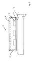
- Fig. 1 shows a schematic cross-sectional view through a first semiconductor module.
- a substrate for example a DCB substrate
- semiconducting components 2 for example power semiconductors, such as diodes, thyristors, IGBTs, MOSFETs or sensor components
- the semiconducting components 2 are partially surrounded by a housing 3.
- the housing 3 can - as in Fig. 1 shown - surround the substrate 1 rarium. But it can also be placed on the substrate 1.
- the reference numeral 4 denotes a potting compound, which the semiconducting components 2 and the substrate 1 at least partially covered and peripherally connected to a circumferential housing wall.
- the semiconductor module H thus constructed is mounted on a heat sink 6 with the interposition of a thermal compound 5.
- the potting compound 4 is formed here from a preceramic polymer, for example polysiloxane, which is filled to about 40 to 50 vol.% With a filler.
- the filler may be a SiC powder having a mean grain size, for example, in the range of 1 to 5 ⁇ m.
- the filler is embedded in the present in gel or thermoset preceramic polymer.
- the potting compound thus formed has an excellent thermal conductivity of more than 10 W / mK.
- a conventional housing 3 are first placed over the substrate 1, so that the substrate 1 rarium adjoins the peripheral housing wall. Subsequently, by a (not shown here) breakthrough in the housing 3, the potting compound 4 are filled. In this case, the preceramic polymer is present in a low-viscosity flowable form. In a next step, the potting compound 4 is then crosslinked, for example by increasing the temperature and placed in a gel-like or thermoset state. Thus, the housing 3 is firmly bonded to the substrate 1.
- the potting compound 4 forms an excellent thermal bridge of the semiconducting devices 2 to the housing 3 and from there into the environment. - A particularly good connection of the potting compound 4 to the housing 3 is achieved, although the housing 3 made of a present in thermosetting preceramic polymer is formed. In this case, the housing 3 has an excellent thermal conductivity ⁇ .
- Fig. 2 shows a schematic cross-sectional view through a second semiconductor module H.
- the in Fig. 1 shown housing 3 omitted.
- the potting compound 4 replaces the housing here. It is shaped in the manner of a housing and covers the semiconductive components 2, at least in sections, an upper side of the substrate 1 facing the semiconducting components 2, and advantageously a peripheral edge of the substrate 1.
- the production of a housing formed in a piece of potting compound 4 can be done for example by using a "lost shape".
- a set with the broken line housing form 7 can be placed on the substrate 1 or put over the substrate 1.
- the housing mold 7 is expediently made of the same material as the potting compound, wherein the preceramic polymer is present here in thermoset form.
- a provided in the housing mold 7 breakthrough (not shown here) poured the potting compound and then also transferred, for example, by a temperature increase in the thermoset state, so that the potting compound 4 and the housing mold 7 form a one-piece housing.
Landscapes
- Structures Or Materials For Encapsulating Or Coating Semiconductor Devices Or Solid State Devices (AREA)
- Cooling Or The Like Of Semiconductors Or Solid State Devices (AREA)
Abstract
Description
- Die Erfindung betrifft ein Halbleitermodul nach dem Oberbegriff des Anspruchs 1.
- Ein solches Halbleitermodul ist beispielsweise aus der
DE 10 2004 021 927 A1 bekannt. Dabei sind mit einem Substrat verbundene halbleitende Bauelemente mit einer elektrisch isolierenden Vergussmasse umgossen. Damit werden die halbleitenden Bauelemente und deren Anschlüsse vor einem Kontakt mit Staub oder Feuchtigkeit geschützt. - Bekannte Vergussmassen, welche beispielsweise auf der Basis von Silikon hergestellt werden, weisen eine relativ niedrige Wärmeleitfähigkeit λ von 0,2 bis 0,3 W/mK auf. Eine beim Betrieb von den halbleitenden Bauelementen erzeugte Wärme wird relativ schlecht abgeführt. Das beschränkt die Leistung des Halbleitermoduls.
- Aufgabe der Erfindung ist es, die Nachteile nach dem Stand der Technik zu beseitigen. Es soll insbesondere ein Halbleitermodul mit verbesserter Wärmeableitung angegeben werden. Nach einem weiteren Ziel der Erfindung soll die Leistung des Halbleitermoduls erhöht werden.
- Diese Aufgabe wird durch die Merkmale des Anspruchs 1 gelöst. Zweckmäßige Ausgestaltungen der Erfindung ergeben sich aus den Merkmalen der Ansprüche 2 bis 9.
- Nach Maßgabe der Erfindung ist vorgesehen, dass die Vergussmasse eine aus einem präkeramischen Polymer gebildete Matrix aufweist. Eine solche Vergussmasse ist elektrisch isolierend. Sie weist eine hervorragende Wärmeleitfähigkeit λ auf. Ein weiterer Vorteil der vorgeschlagenen Vergussmasse ist deren hohe Temperaturbeständigkeit. Sie hält Betriebstemperaturen von bis zu 300°C stand.
- Im Sinne der vorliegenden Erfindung wird unter dem Begriff "Substrat" ein z. B. in Form einer Platte vorliegendes elektrisch isolierendes Material verstanden, welches mit Leiterbahnen versehen ist. Darauf kann zumindest ein halbleitendes Bauelement beispielsweise mittels eines Lots, eines Klebstoffs oder dgl. montiert sein.
- Unter dem Begriff "umgossen" wird im Sinne der vorliegenden Erfindung verstanden, dass ein mit dem Substrat zuvor verbundenes halbleitendes Bauelement nachfolgend mit der Vergussmasse übergossen wird. Infolgedessen überdeckt die Vergussmasse das halbleitende Bauelement, d. h. umgreift dessen seitliche Wände sowie dessen Oberseite. Eine dem Substrat zugewandte Unterseite des halbleitenden Bauelements ist dagegen nicht oder nur teilweise mit der Vergussmasse in Kontakt.
- Unter dem Begriff "präkeramisches Polymer" wird ein Polymer verstanden, welches z. B. mit zunehmender Temperatur zunächst in einen gelartigen und nachfolgend in einen duroplastischen Zustand übergeht. Im duroplastischen Zustand weist ein präkeramisches Polymer in der Regel eine Temperaturbeständigkeit von bis zu 300°C auf. Bei einer weiteren Temperaturerhöhung können aus präkeramischen Polymeren keramische Werkstoffe hergestellt werden. Zu präkeramischen Polymeren gehören beispielsweise Polysilane, Polycarbosilane und Polyorganosilazane.
- Nach einer vorteilhaften Ausgestaltung ist vorgesehen, dass das präkeramische Polymer mit einem Füllgrad von bis zu 80 Vol.% mit einem Füllstoff gefüllt ist. Damit können die Wärmeleitfähigkeit und die Viskosität des präkeramischen Polymers erhöht werden.
- Zweckmäßigerweise handelt es sich bei dem Füllstoff um ein aus einem keramischen Material gebildetes Pulver mit einer mittleren Korngröße im Bereich von 0,5 bis 500 µm. Das vorgeschlagene keramische Material ist weitgehend inert. Dessen Zusatz führt nicht zu unerwünschten chemischen Reaktionen mit dem präkeramischen Polymer. Die vorgeschlagene mittlere Korngröße ermöglicht ein Vergießen der Vergussmasse mit herkömmlichen Vorrichtungen.
- Die Wärmeleitfähigkeit λ des keramischen Materials ist zweckmäßigerweise bei Raumtemperatur größer als 10 W/mK, vorzugsweise größer als 20 W/mK. Je nach Füllgrad gelingt es damit, die Wärmeleitfähigkeit des mit dem keramischen Material gefüllten präkeramischen Polymers auf Werte oberhalb 2 W/mK zu steigern. Damit eignet sich die vorgeschlagene Vergussmasse insbesondere zur Herstellung eines im Betrieb eine relativ große Wärme freisetzenden Leistungshalbleitermoduls.
- Das keramische Material ist zweckmäßigerweise aus der folgenden Gruppe ausgewählt: BN, SiC, Si3N4, AlN, Steatit, Cordierit. Die vorgeschlagenen keramischen Materialien zeichnen sich durch eine hohe Wärmeleitfähigkeit aus.
- Weiterhin hat es sich als zweckmäßig erwiesen, dass das präkeramische Polymer aus der folgenden Gruppe ausgewählt ist: Polysiloxan, Polysilazan, Polycarbosilan.
- Üblicherweise ist beim Halbleitermodul ein das halbleitende Bauelement zumindest abschnittsweise umgebendes Gehäuse vorgesehen. Ein solches Gehäuse ist in der Regel aus einem Polymer hergestellt. Das Gehäuse wird üblicherweise mit dem Substrat verbunden, nachdem darauf das halbleitende Bauelement montiert worden ist.
- Nach einer vorteilhaften Ausgestaltung der Erfindung ist vorgesehen, dass ein Zwischenraum zwischen dem halbleitenden Bauelement und einem das halbleitende Bauelement umgebenden Gehäuse zumindest teilweise mit der Vergussmasse gefüllt ist. Damit bildet die Vergussmasse eine wärmeleitende Brücke zwischen dem halbleitenden Bauelement und dem Gehäuse.
- Die Vergussmasse wird üblicherweise in einem niedrigviskosen Zustand vergossen. Damit können Kapillarkräfte ausgenutzt und ein besonders guter thermischer Kontakt zwischen der Vergussmasse und dem halbleitenden Bauelement gewährleistet werden. Nachfolgend kann das präkeramische Polymer beispielsweise durch Temperaturerhöhung, Strahlungsbehandlung oder dgl. bis zu einem vorgegebenen Grad vernetzt werden. Das präkeramische Polymer kann dann also insbesondere in gelartiger oder duroplastischer Form vorliegen.
- Nach einer besonders vorteilhaften alternativen Ausgestaltung ermöglicht die Verwendung der erfindungsgemäßen Vergussmasse auch die Weglassung des zur Herstellung von Halbleitermodulen üblicherweise verwendeten Gehäuses. Ein das halbleitende Bauelement umgebendes Gehäuse kann in einstückiger Ausbildung mit der Vergussmasse aus dem in duroplastischer Form vorliegenden präkeramischen Polymer gebildet sein. D. h. das mit dem Substrat verbundene halbleitende Bauelement kann z. B. mit einer Form umgeben werden, in welche anschließend die Vergussmasse eingegossen und dann in die duroplastische Form überführt wird. In diesem Fall bildet also die Vergussmasse das Gehäuse. Bei der Form kann es sich auch um eine "verlorene Form" handeln, beispielsweise um einen auf das Substrat aufgesetzten und das halbleitende Bauelement umgebenden Rahmen. Der Rahmen weist in diesem Fall zweckmäßigerweise eine aus dem präkeramischen Polymer gebildete Matrix auf. Dabei liegt die präkeramische Matrix in duroplastischer Form vor. Zweckmäßigerweise weist der Rahmen dieselbe Materialzusammensetzung wie die Vergussmasse auf. Die vorgeschlagene verlorene Form kann vor dem Einfüllen der Vergussmasse auch mit dem Substrat, beispielsweise wiederum mittels eines präkeramischen Polymers, verklebt werden. Damit wird eine besonders gute Abdichtung zwischen dem Rahmen und dem Substrat erreicht.
- Nachfolgend werden Ausführungsbeispiele der Erfindung anhand der Figuren näher erläutert. Es zeigen:
- Fig. 1
- eine schematische Querschnittsansicht durch ein erstes Halbleitermodul und
- Fig. 2
- eine schematische Querschnittsansicht durch ein zweites Halbleitermodul.
-
Fig. 1 zeigt eine schematische Querschnittsansicht durch ein erstes Halbleitermodul. Auf einem Substrat 1, beispielsweise einem DCB-Substrat, sind mehrere halbleitenden Bauelemente 2, beispielsweise Leistungshalbleiter, wie Dioden, Thyristoren, IGBTs, MOSFETs oder Sensorbauelemente, mittels einer Lötverbindung montiert. Die halbleitenden Bauelemente 2 sind abschnittsweise von einem Gehäuse 3 umgeben. Das Gehäuse 3 kann - wie inFig. 1 gezeigt - das Substrat 1 randlich umgreifen. Es kann aber auch auf das Substrat 1 aufgesetzt sein. Mit dem Bezugszeichen 4 ist eine Vergussmasse bezeichnet, welche die halbleitenden Bauelemente 2 und das Substrat 1 zumindest abschnittsweise überdeckt und randlich an eine umlaufende Gehäusewand anschließt. Das so beschaffene Halbleitermodul H ist unter Zwischenschaltung einer Wärmeleitpaste 5 auf einen Kühlkörper 6 montiert. - Die Vergussmasse 4 ist hier aus einem präkeramischen Polymer, beispielsweise Polysiloxan, gebildet, welches zu etwa 40 bis 50 Vol.% mit einem Füllstoff gefüllt ist. Bei dem Füllstoff kann es sich um ein SiC-Pulver mit einer mittleren Korngröße beispielsweise im Bereich von 1 bis 5 µm handeln. Der Füllstoff ist in das in gelartiger oder duroplastischer Form vorliegende präkeramische Polymer eingebettet. Die so gebildete Vergussmasse weist eine hervorragende Wärmeleitfähigkeit von mehr als 10 W/mK auf.
- Zur Herstellung des in
Fig. 1 gezeigten Halbleitermoduls kann beispielsweise ein herkömmliches Gehäuse 3 zunächst über das Substrat 1 gestülpt werden, so dass das Substrat 1 randlich an die umlaufende Gehäusewand anschließt. Anschließend kann durch einen (hier nicht gezeigten) Durchbruch im Gehäuse 3 die Vergussmasse 4 eingefüllt werden. Dabei liegt das präkeramische Polymer in einer niedrig viskosen fließfähigen Form vor. In einem nächsten Schritt wird die Vergussmasse 4 sodann beispielsweise durch Temperaturerhöhung vernetzt und in einen gelartigen oder duroplastischen Zustand versetzt. Damit wird das Gehäuse 3 fest mit dem Substrat 1 verklebt. Die Vergussmasse 4 bildet eine hervorragende Wärmebrücke von den halbleitenden Bauelementen 2 zum Gehäuse 3 und von da in die Umgebung. - Eine besonders gute Anbindung der Vergussmasse 4 an das Gehäuse 3 wird erreicht, wenn auch das Gehäuse 3 aus einem in duroplastischer Form vorliegenden präkeramischen Polymer gebildet ist. In diesem Fall weist auch das Gehäuse 3 eine hervorragende Wärmeleitfähigkeit λ auf. -
Fig. 2 zeigt eine schematische Querschnittsansicht durch ein zweites Halbleitermodul H. Hier ist das inFig. 1 gezeigte Gehäuse 3 weggelassen. Die Vergussmasse 4 ersetzt hier das Gehäuse. Sie ist nach Art eines Gehäuses geformt und überdeckt die halbleitenden Bauelemente 2, zumindest abschnittsweise eine den halbleitenden Bauelementen 2 zugewandte Oberseite des Substrats 1 sowie vorteilhafterweise einen umlaufenden Rand des Substrats 1. - Die Herstellung eines in einem Stück der Vergussmasse 4 gebildeten Gehäuses kann beispielsweise unter Verwendung einer "verlorenen Form" erfolgen. Dazu kann zunächst eine mit der unterbrochenen Linie kenntlich gemachte Gehäuseform 7 auf das Substrat 1 gesetzt oder auch über das Substrat 1 gestülpt werden. Die Gehäuseform 7 ist dabei zweckmäßigerweise aus demselben Material wie die Vergussmasse hergestellt, wobei das präkeramische Polymer hier in duroplastischer Form vorliegt. Anschließend wird durch einen in der Gehäuseform 7 vorgesehenen Durchbruch (hier nicht gezeigt) die Vergussmasse eingegossen und nachfolgend beispielsweise durch eine Temperaturerhöhung ebenfalls in den duroplastischen Zustand überführt, so dass die Vergussmasse 4 und die Gehäuseform 7 ein einstückiges Gehäuse bilden.
-
- 1
- Substrat
- 2
- halbleitendes Bauelement
- 3
- Gehäuse
- 4
- Vergussmasse
- 5
- Wärmeleitpaste
- 6
- Kühlkörper
- 7
- Gehäuseform
- H
- Halbleitermodul
Claims (9)
- Halbleitermodul, insbesondere Leistungshalbleitermodul, bei dem ein mit einem Substrat (1) verbundenes halbleitendes Bauelement (2) mit einer elektrisch isolierenden Vergussmasse (4) umgossen ist,
dadurch gekennzeichnet, dass
die Vergussmasse (4) eine aus einem präkeramischen Polymer gebildete Matrix aufweist. - Halbleitermodul nach Anspruch 1, wobei das präkeramische Polymer mit einem Füllgrad von bis zu 80 Vol.% mit einem Füllstoff gefüllt ist.
- Halbleitermodul nach einem der vorhergehenden Ansprüche, wobei der Füllstoff ein aus einem keramischen Material gebildetes Pulver mit einer mittleren Korngröße im Bereich von 0,5 bis 500 µm ist.
- Halbleitermodul nach einem der vorhergehenden Ansprüche, wobei die Wärmeleitfähigkeit λ des keramischen Materials bei Raumtemperatur größer als 10 W/mK, vorzugsweise größer als 20 W/mK, ist.
- Halbleitermodul nach einem der vorhergehenden Ansprüche, wobei das keramische Material aus der folgenden Gruppe ausgewählt ist: BN, SiC, Si3N4, AlN, Steatit, Cordierit.
- Halbleitermodul nach einem der vorhergehenden Ansprüche, wobei das präkeramische Polymer aus der folgenden Gruppe ausgewählt ist: Polysiloxan, Polysilazan, Polycarbosilan.
- Halbleitermodul nach einem der vorhergehenden Ansprüche, wobei ein Zwischenraum zwischen dem halbleitenden Bauelement (2) und einem das halbleitende Bauelement (2) zumindest abschnittsweise umgebenden Gehäuse (3) zumindest teilweise mit Vergussmasse (4) gefüllt ist.
- Halbleitermodul nach einem der vorhergehenden Ansprüche, wobei das präkeramische Polymer in gelartiger oder duroplastischer Form vorliegt.
- Halbleitermodul nach einem der Ansprüche 1 bis 6, wobei ein das halbleitende Bauelement (2) umgebendes Gehäuse (3) in einstückiger Ausbildung mit der Vergussmasse (4) aus dem in duroplastischen Form vorliegenden präkeramischen Polymer gebildet ist.
Applications Claiming Priority (1)
| Application Number | Priority Date | Filing Date | Title |
|---|---|---|---|
| DE102009000884A DE102009000884B3 (de) | 2009-02-16 | 2009-02-16 | Halbleitermodul mit Gehäuse aus präkeramischem Polymer |
Publications (2)
| Publication Number | Publication Date |
|---|---|
| EP2219217A2 true EP2219217A2 (de) | 2010-08-18 |
| EP2219217A3 EP2219217A3 (de) | 2010-11-03 |
Family
ID=42181545
Family Applications (1)
| Application Number | Title | Priority Date | Filing Date |
|---|---|---|---|
| EP20090016025 Withdrawn EP2219217A3 (de) | 2009-02-16 | 2009-12-24 | Halbleitermodul |
Country Status (3)
| Country | Link |
|---|---|
| EP (1) | EP2219217A3 (de) |
| CN (1) | CN101807564A (de) |
| DE (1) | DE102009000884B3 (de) |
Families Citing this family (1)
| Publication number | Priority date | Publication date | Assignee | Title |
|---|---|---|---|---|
| DE102014211464A1 (de) * | 2014-06-16 | 2015-12-17 | Robert Bosch Gmbh | Halbleitermodul mit einer elektrisch isolierten Wärmesenke |
Citations (6)
| Publication number | Priority date | Publication date | Assignee | Title |
|---|---|---|---|---|
| EP0369652A2 (de) * | 1988-11-12 | 1990-05-23 | Kureha Kagaku Kogyo Kabushiki Kaisha | Harzzusammensetzungen zum Abdichten von elektronischen Bauelementen und abgedichtete elektronische Bauelemente |
| US5436084A (en) | 1994-04-05 | 1995-07-25 | Dow Corning Corporation | Electronic coatings using filled borosilazanes |
| US5563102A (en) * | 1993-02-26 | 1996-10-08 | Dow Corning Corporation | Method of sealing integrated circuits |
| US6319740B1 (en) | 1995-10-27 | 2001-11-20 | Honeywell International Inc. | Multilayer protective coating for integrated circuits and multichip modules and method of applying same |
| EP1336990A1 (de) * | 2002-02-14 | 2003-08-20 | Abb Research Ltd. | Gehäuse für ein hochspannungsfestes Leistungshalbleitermodul |
| DE102004021927A1 (de) | 2004-05-04 | 2005-12-01 | Semikron Elektronik Gmbh & Co. Kg | Verfahren zur inneren elektrischen Isolation eines Substrats für ein Leistungshalbleitermodul |
Family Cites Families (3)
| Publication number | Priority date | Publication date | Assignee | Title |
|---|---|---|---|---|
| US5436083A (en) * | 1994-04-01 | 1995-07-25 | Dow Corning Corporation | Protective electronic coatings using filled polysilazanes |
| US5635240A (en) * | 1995-06-19 | 1997-06-03 | Dow Corning Corporation | Electronic coating materials using mixed polymers |
| JP2006206721A (ja) * | 2005-01-27 | 2006-08-10 | Kansai Electric Power Co Inc:The | 高耐熱合成高分子化合物及びこれで被覆した高耐電圧半導体装置 |
-
2009
- 2009-02-16 DE DE102009000884A patent/DE102009000884B3/de not_active Expired - Fee Related
- 2009-12-24 EP EP20090016025 patent/EP2219217A3/de not_active Withdrawn
-
2010
- 2010-02-09 CN CN201010116688.1A patent/CN101807564A/zh active Pending
Patent Citations (6)
| Publication number | Priority date | Publication date | Assignee | Title |
|---|---|---|---|---|
| EP0369652A2 (de) * | 1988-11-12 | 1990-05-23 | Kureha Kagaku Kogyo Kabushiki Kaisha | Harzzusammensetzungen zum Abdichten von elektronischen Bauelementen und abgedichtete elektronische Bauelemente |
| US5563102A (en) * | 1993-02-26 | 1996-10-08 | Dow Corning Corporation | Method of sealing integrated circuits |
| US5436084A (en) | 1994-04-05 | 1995-07-25 | Dow Corning Corporation | Electronic coatings using filled borosilazanes |
| US6319740B1 (en) | 1995-10-27 | 2001-11-20 | Honeywell International Inc. | Multilayer protective coating for integrated circuits and multichip modules and method of applying same |
| EP1336990A1 (de) * | 2002-02-14 | 2003-08-20 | Abb Research Ltd. | Gehäuse für ein hochspannungsfestes Leistungshalbleitermodul |
| DE102004021927A1 (de) | 2004-05-04 | 2005-12-01 | Semikron Elektronik Gmbh & Co. Kg | Verfahren zur inneren elektrischen Isolation eines Substrats für ein Leistungshalbleitermodul |
Also Published As
| Publication number | Publication date |
|---|---|
| EP2219217A3 (de) | 2010-11-03 |
| CN101807564A (zh) | 2010-08-18 |
| DE102009000884B3 (de) | 2010-10-07 |
Similar Documents
| Publication | Publication Date | Title |
|---|---|---|
| DE102013220880B4 (de) | Elektronisches Halbleitergehäuse mit einer elektrisch isolierenden, thermischen Schnittstellenstruktur auf einer Diskontinuität einer Verkapselungsstruktur sowie ein Herstellungsverfahren dafür und eine elektronische Anordung dies aufweisend | |
| DE102012224355B4 (de) | Leistungsmodul | |
| DE102015118245B4 (de) | Elektronische Komponente mit einem thermischen Schnittstellenmaterial, Herstellungsverfahren für eine elektronische Komponente, Wärmeabfuhrkörper mit einem thermischen Schnittstellenmaterial und thermisches Schnittstellenmaterial | |
| DE102014213564B4 (de) | Halbleitervorrichtung und Verfahren zu ihrer Herstellung | |
| EP3747048A1 (de) | Elektronisches bauelement | |
| DE102014104856B4 (de) | Explosionsgeschütztes Leistungshalbleitermodul | |
| EP3066684A1 (de) | Halbleitermodul mit einer einen halbleiterbaustein bedeckenden umhüllungsmasse aus zement | |
| DE102016117843A1 (de) | Mit Kühlfluid gekühlte und eine Abschirmschicht umfassende Packung | |
| DE102016107495A1 (de) | Vielschicht-Trägersystem, Verfahren zur Herstellung eines Vielschicht-Trägersystems und Verwendung eines Vielschicht-Trägersystems | |
| DE102014100282A1 (de) | Chip-anordnung, verfahren zur herstellung einer chip-anordnung, integrierte schaltungen und verfahren zur herstellung einer integrierten schaltung | |
| DE102009044863A1 (de) | Halbleiter-Bauelement | |
| DE112018001769T5 (de) | Leistungsmodul und herstellungsverfahren des leistungsmoduls | |
| DE102015115132B4 (de) | Halbleitermodul mit integrierter Stift- oder Rippenkühlstruktur und Verfahren zu seiner Herstellung | |
| EP2219213B1 (de) | Halbleiteranordnung | |
| DE102014213545A1 (de) | Leistungshalbleitermodul | |
| DE102015102041A1 (de) | Leistungsmodul | |
| DE102009000884B3 (de) | Halbleitermodul mit Gehäuse aus präkeramischem Polymer | |
| EP2278616B1 (de) | Leistungshalbleitermodul mit einem Sandwich mit einem Leistungshalbleiterbauelement | |
| DE102009000882A1 (de) | Substrat zur Aufnahme mindestens eines Bauelements und Verfahren zur Herstellung eines Substrats | |
| EP2219216B1 (de) | Halbleitermodul | |
| DE102009000883A1 (de) | Substrat zur Aufnahme mindestens eines Bauelements und Verfahren zur Herstellung eines Substrats | |
| DE102019132314A1 (de) | Package mit Einkapselung unter Kompressionsbelastung | |
| WO2023094390A1 (de) | Elektronisches bauelement und verfahren zum herstellen eines elektronischen bauelements | |
| DE102015223466A1 (de) | Elektrische Vorrichtung mit einer Umhüllmasse | |
| EP2947687A2 (de) | Leistungshalbleitermodul |
Legal Events
| Date | Code | Title | Description |
|---|---|---|---|
| PUAI | Public reference made under article 153(3) epc to a published international application that has entered the european phase |
Free format text: ORIGINAL CODE: 0009012 |
|
| AK | Designated contracting states |
Kind code of ref document: A2 Designated state(s): AT BE BG CH CY CZ DE DK EE ES FI FR GB GR HR HU IE IS IT LI LT LU LV MC MK MT NL NO PL PT RO SE SI SK SM TR |
|
| AX | Request for extension of the european patent |
Extension state: AL BA RS |
|
| PUAL | Search report despatched |
Free format text: ORIGINAL CODE: 0009013 |
|
| AK | Designated contracting states |
Kind code of ref document: A3 Designated state(s): AT BE BG CH CY CZ DE DK EE ES FI FR GB GR HR HU IE IS IT LI LT LU LV MC MK MT NL NO PL PT RO SE SI SK SM TR |
|
| AX | Request for extension of the european patent |
Extension state: AL BA RS |
|
| 17P | Request for examination filed |
Effective date: 20101014 |
|
| 17Q | First examination report despatched |
Effective date: 20110916 |
|
| STAA | Information on the status of an ep patent application or granted ep patent |
Free format text: STATUS: THE APPLICATION HAS BEEN WITHDRAWN |
|
| 18W | Application withdrawn |
Effective date: 20150821 |