EP2216877A1 - Gleichstromwandler und Verfahren zur Steuerung des Gleichstromwandlers - Google Patents
Gleichstromwandler und Verfahren zur Steuerung des Gleichstromwandlers Download PDFInfo
- Publication number
- EP2216877A1 EP2216877A1 EP09001630A EP09001630A EP2216877A1 EP 2216877 A1 EP2216877 A1 EP 2216877A1 EP 09001630 A EP09001630 A EP 09001630A EP 09001630 A EP09001630 A EP 09001630A EP 2216877 A1 EP2216877 A1 EP 2216877A1
- Authority
- EP
- European Patent Office
- Prior art keywords
- switching element
- phase
- voltage
- sub
- mode
- Prior art date
- Legal status (The legal status is an assumption and is not a legal conclusion. Google has not performed a legal analysis and makes no representation as to the accuracy of the status listed.)
- Granted
Links
- 238000000034 method Methods 0.000 title claims description 13
- 230000001939 inductive effect Effects 0.000 claims abstract description 40
- 238000001514 detection method Methods 0.000 claims abstract description 37
- 230000005669 field effect Effects 0.000 claims abstract description 13
- 230000008878 coupling Effects 0.000 claims description 6
- 238000010168 coupling process Methods 0.000 claims description 6
- 238000005859 coupling reaction Methods 0.000 claims description 6
- 230000033228 biological regulation Effects 0.000 claims description 5
- 238000006243 chemical reaction Methods 0.000 description 39
- 238000010586 diagram Methods 0.000 description 10
- 230000001965 increasing effect Effects 0.000 description 5
- 239000013256 coordination polymer Substances 0.000 description 4
- 230000006378 damage Effects 0.000 description 2
- 230000007423 decrease Effects 0.000 description 2
- 230000003247 decreasing effect Effects 0.000 description 2
- 230000001419 dependent effect Effects 0.000 description 1
- 238000011161 development Methods 0.000 description 1
- 230000018109 developmental process Effects 0.000 description 1
- 238000007599 discharging Methods 0.000 description 1
- 238000012986 modification Methods 0.000 description 1
- 230000004048 modification Effects 0.000 description 1
- 239000004065 semiconductor Substances 0.000 description 1
Images

Classifications
-
- H—ELECTRICITY
- H02—GENERATION; CONVERSION OR DISTRIBUTION OF ELECTRIC POWER
- H02M—APPARATUS FOR CONVERSION BETWEEN AC AND AC, BETWEEN AC AND DC, OR BETWEEN DC AND DC, AND FOR USE WITH MAINS OR SIMILAR POWER SUPPLY SYSTEMS; CONVERSION OF DC OR AC INPUT POWER INTO SURGE OUTPUT POWER; CONTROL OR REGULATION THEREOF
- H02M3/00—Conversion of dc power input into dc power output
- H02M3/02—Conversion of dc power input into dc power output without intermediate conversion into ac
- H02M3/04—Conversion of dc power input into dc power output without intermediate conversion into ac by static converters
- H02M3/10—Conversion of dc power input into dc power output without intermediate conversion into ac by static converters using discharge tubes with control electrode or semiconductor devices with control electrode
- H02M3/145—Conversion of dc power input into dc power output without intermediate conversion into ac by static converters using discharge tubes with control electrode or semiconductor devices with control electrode using devices of a triode or transistor type requiring continuous application of a control signal
- H02M3/155—Conversion of dc power input into dc power output without intermediate conversion into ac by static converters using discharge tubes with control electrode or semiconductor devices with control electrode using devices of a triode or transistor type requiring continuous application of a control signal using semiconductor devices only
- H02M3/156—Conversion of dc power input into dc power output without intermediate conversion into ac by static converters using discharge tubes with control electrode or semiconductor devices with control electrode using devices of a triode or transistor type requiring continuous application of a control signal using semiconductor devices only with automatic control of output voltage or current, e.g. switching regulators
- H02M3/158—Conversion of dc power input into dc power output without intermediate conversion into ac by static converters using discharge tubes with control electrode or semiconductor devices with control electrode using devices of a triode or transistor type requiring continuous application of a control signal using semiconductor devices only with automatic control of output voltage or current, e.g. switching regulators including plural semiconductor devices as final control devices for a single load
- H02M3/1588—Conversion of dc power input into dc power output without intermediate conversion into ac by static converters using discharge tubes with control electrode or semiconductor devices with control electrode using devices of a triode or transistor type requiring continuous application of a control signal using semiconductor devices only with automatic control of output voltage or current, e.g. switching regulators including plural semiconductor devices as final control devices for a single load comprising at least one synchronous rectifier element
-
- H—ELECTRICITY
- H02—GENERATION; CONVERSION OR DISTRIBUTION OF ELECTRIC POWER
- H02M—APPARATUS FOR CONVERSION BETWEEN AC AND AC, BETWEEN AC AND DC, OR BETWEEN DC AND DC, AND FOR USE WITH MAINS OR SIMILAR POWER SUPPLY SYSTEMS; CONVERSION OF DC OR AC INPUT POWER INTO SURGE OUTPUT POWER; CONTROL OR REGULATION THEREOF
- H02M1/00—Details of apparatus for conversion
- H02M1/0003—Details of control, feedback or regulation circuits
- H02M1/0016—Control circuits providing compensation of output voltage deviations using feedforward of disturbance parameters
- H02M1/0022—Control circuits providing compensation of output voltage deviations using feedforward of disturbance parameters the disturbance parameters being input voltage fluctuations
-
- H—ELECTRICITY
- H02—GENERATION; CONVERSION OR DISTRIBUTION OF ELECTRIC POWER
- H02M—APPARATUS FOR CONVERSION BETWEEN AC AND AC, BETWEEN AC AND DC, OR BETWEEN DC AND DC, AND FOR USE WITH MAINS OR SIMILAR POWER SUPPLY SYSTEMS; CONVERSION OF DC OR AC INPUT POWER INTO SURGE OUTPUT POWER; CONTROL OR REGULATION THEREOF
- H02M1/00—Details of apparatus for conversion
- H02M1/0045—Converters combining the concepts of switch-mode regulation and linear regulation, e.g. linear pre-regulator to switching converter, linear and switching converter in parallel, same converter or same transistor operating either in linear or switching mode
-
- Y—GENERAL TAGGING OF NEW TECHNOLOGICAL DEVELOPMENTS; GENERAL TAGGING OF CROSS-SECTIONAL TECHNOLOGIES SPANNING OVER SEVERAL SECTIONS OF THE IPC; TECHNICAL SUBJECTS COVERED BY FORMER USPC CROSS-REFERENCE ART COLLECTIONS [XRACs] AND DIGESTS
- Y02—TECHNOLOGIES OR APPLICATIONS FOR MITIGATION OR ADAPTATION AGAINST CLIMATE CHANGE
- Y02B—CLIMATE CHANGE MITIGATION TECHNOLOGIES RELATED TO BUILDINGS, e.g. HOUSING, HOUSE APPLIANCES OR RELATED END-USER APPLICATIONS
- Y02B70/00—Technologies for an efficient end-user side electric power management and consumption
- Y02B70/10—Technologies improving the efficiency by using switched-mode power supplies [SMPS], i.e. efficient power electronics conversion e.g. power factor correction or reduction of losses in power supplies or efficient standby modes
Definitions
- the invention relates to a DC/DC converter and to a method for controlling a DC/DC converter.
- the power supply of electric circuits is achieved by DC/DC converters which are able to convert an input DC voltage to an output DC voltage being different from the input DC voltage. If a desired output voltage is higher than the input voltage, an up conversion has to be performed which is achieved, for example, by boost converters. If, however, the desired output voltage is lower than the input voltage, a down conversion has to be performed which is achieved, for example, by linear regulators or buck converters.
- both up and down conversion may be needed due to changing input or output voltages.
- a down conversion is needed, whereas after discharging of the battery, up conversion of the input voltage may be needed.
- buck-boost converters are used being able to convert the input voltage up and down.
- An embodiment of a DC/DC converter comprises an input connection to receive an input voltage, an output connection to provide an output voltage and a reference potential connection.
- An inductive element has a first terminal connected to the input connection and a second terminal coupled to the reference potential connection by a first switching element.
- a second switching element couples the second terminal of the inductive element to the output connection, wherein the second switching element is a p-channel field-effect transistor, P-FET.
- a control unit comprises a detection unit which is configured to detect a first mode of operation in which the input voltage is higher than a desired value of the output voltage. The control unit is configured, upon detection of the first mode of operation, during a first phase, to control the first switching element to a close state and a second switching element to an open state.
- the control unit controls the first switching element to an open state.
- the second switching element is controlled to a closed state and, during the second sub-phase, the control unit provides a control voltage to a gate terminal of the second switching element which is higher than the difference between the output voltage and a threshold voltage of the second switching element.
- the inductive element is coupled between the input connection and the reference potential connection such that current flows through the inductive element and energy is stored within.
- the first switching element is in an open state such that no current can flow from the second terminal of the inductive element to the reference potential connection.
- a current can flow from the second terminal of the inductive element to the output connection via the fully closed second switching element.
- the p-channel field-effect transistor is conducting with a high resistance. As a consequence, less energy is transferred from the inductive element to the output connection, thus enabling a down conversion.
- the overall efficiency of the DC/DC converter during a down conversion is improved compared, for example, to a conventional buck converter or a low dropout regulator.
- the control unit can, for example, use the voltage at the output connection, thus the output voltage, as the control voltage provided to the gate terminal of the second switching element.
- control unit is configured, upon detection of the first mode of operation, during the second sub-phase, to provide a control voltage to the gate terminal of the second switching element which is higher than the difference between the input voltage and the threshold voltage of the second switching element.
- control unit uses the input voltage as the control voltage to be provided to the gate terminal.
- the second phase upon detection of the first mode of operation, comprises at least one further sub-phase during which the second switching element is controlled according to the control of the first sub-phase or of the second sub-phase.
- the second phase comprises a sequence of a first sub-phase, a second sub-phase and a third sub-phase being equivalent to the first sub-phase with respect to the control of the second switching element. Durations of first and third sub-phase can differ from each other.
- the second phase comprises a sequence of a second sub-phase, a first sub-phase and a third sub-phase being equivalent to the second sub-phase with respect to the switch control.
- the order of the first and the second sub-phase within the second phase can be chosen arbitrarily. Furthermore, the number of sub-phases within the second phase is theoretically unlimited, but may be limited practically. For example, on the one hand, with a greater number of sub-phases, a smoother provision of current to the output connection can be achieved. On the other hand, switching of the P-FET usually causes losses.
- the second phase preferably only comprises sub-phases during which the switching elements are controlled according to the first and the second sub-phase.
- the DC/DC converter or the control unit, respectively, can be operated based on a reference clock signal provided externally or generated internally. Accordingly, in one embodiment, upon detection of the first mode of operation, the first phase and the second phase are alternating within clock periods determined by the reference clock signal.
- the output voltage is controlled by the control unit. For example, upon detection of the first mode of operation, a duration of the first phase is set depending on the desired value of the output voltage.
- duration of the first sub-phase or of the second sub-phase is adjusted depending on at least one of the following: a ratio between the input voltage and the output voltage, a current drawn by a load connected to the output connection, a desired line regulation value. For example, a duration of the first sub-phase can be decreased if a ratio between the input voltage and the output voltage decreases. If an output current of the DC/DC converter is measured, the duration of the first sub-phase can be increased for an increasing output current.
- line regulation that is the capability to maintain a constant output voltage despite changes to the input voltage, can be influenced by the respective durations of the first and the second sub-phase.
- the first switching element is an n-channel field-effect transistor, N-FET.
- the first and the second switching elements being an N-FET and a P-FET are field-effect transistors of an enhancement type.
- the N-FET and the P-FET are normally off, that is in an open state.
- a charge store is connected to the output connection.
- the charge store is connected between the output connection and the reference potential connection. Accordingly, a current provided by the inductive element during the second phase can be used to charge the charge store to the desired value of the output voltage. Furthermore, the output voltage can be buffered by the charge store.
- the embodiments described above are related to down conversion, i.e. where the input voltage is higher than the desired value of the output voltage.
- the structure of the DC/DC converter can also be used for up conversion, i.e. wherein the input voltage is lower than the desired value of the output voltage.
- the detection unit is configured to detect a second mode of operation in which the input voltage is lower than the desired value of the output voltage.
- the control unit is configured, upon detection of the second mode of operation, to alternately and conversely control the first switching element and the second switching element between an open state and a closed state, wherein a respective duty cycle is depending on the desired value of the output voltage.
- one switching element of the first and the second switching element is in an open state while the other switching element is in a closed state. If the first switching element is in a closed state, energy is stored in the inductive element, whereas, if the second switching element is in the closed state, energy is transferred from the inductive element to the output connection.
- the dependency of the above-mentioned duty cycle with respect to the desired output voltage is not described in detail here, as such control is well known in the art.
- the detection unit is configured to detect a third mode of operation in which the output voltage is higher than the desired value of the output voltage.
- the control unit is configured, upon detection of the third mode of operation, to control both the first switching element and the second switching element to an open state.
- the detection unit is, for example, configured to detect a maximum voltage within the DC/DC converter.
- the control unit is then configured to provide said maximum voltage to the bulk terminal of the second switching element.
- the DC/DC converter comprises an input connection to receive an input voltage, an output connection to provide an output voltage, a reference potential connection, an inductive element having a first terminal connected to the input connection, a first switching element coupling a second terminal of the inductive element to the reference potential connection, and a second switching element coupling the second terminal of the inductive element to the output connection, the second switching element being a p-channel field-effect transistor, P-FET.
- a first mode of operation is detected in which the input voltage is higher than a desired value of the output voltage, and, upon detection of the first mode of operation, the following is performed.
- the first switching element is controlled to a closed state and the second switching element is controlled to an open state.
- a second phase which comprises a first sub-phase and a second sub-phase, the first switching element is controlled to an open state.
- the second switching element is controlled to a closed state and, during the second sub-phase, a control voltage is provided to a gate terminal of the second switching element which is higher than a difference between the output voltage and a threshold voltage of the second switching element.
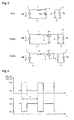
- FIG. 1 shows an embodiment of a DC/DC converter comprising an input connection 1, an output connection 2 and a reference potential connection 3.
- An inductive element L has a first terminal connected to the input connection 1 and a second terminal 4.
- the second terminal 4 is coupled to the reference potential connection 3 by means of a first switching element N1 which is embodied as an n-channel field-effect transistor, N-FET.
- the second terminal 4 of the inductive element L is further coupled to the output connection 2 by means of second switching element P1 which is embodied as a p-channel field-effect transistor, P-FET.
- a charge store C is connected between the output connection 2 and the reference potential connection 3.
- the DC/DC converter further comprises a control unit CTL comprising input terminals D1, D2, D4 and output terminals CN, CP, CB.
- the control unit CTL further comprises a clock input CLK for receiving a reference clock signal.
- the input terminal D1 is connected to the input connection 1 for detecting or measuring an input voltage VIN at the input connection 1.
- the input terminal D2 is connected to the output connection 2 for measuring or detecting an output voltage VOUT.
- the input terminal D4 is connected to the second terminal 4 of the inductive element for measuring or detecting a voltage V4 at said terminal 4.
- Output terminal CN is connected to a control terminal of the N-FET N1, output terminal CP is connected to the gate terminal GP1 of the P-FET P1.
- Output terminal CB is connected to a bulk terminal BP1 of the P-FET P1.
- the field-effect transistors N1, P1 are of the enhancement type in this embodiment. In other words, the transistors are normally off or non-conducting if no control voltage is applied to their gate terminals.
- the DC/DC converter can be operated in various modes of operation. For example, in a first mode of operation, the input voltage VIN is higher than a desired value of the output voltage VOUT, thus resulting in the need for a down conversion. Accordingly, in a first mode of operation, the DC/DC converter is configured for down converting the input voltage VIN. In a second mode of operation, the input voltage VIN is lower than a desired value of the output voltage VOUT, such that an up conversion is needed. Accordingly, in a second mode of operation, the DC/DC converter is configured for up converting the input voltage VIN.
- the charge store C is charged to an actual value of the output voltage. If said actual output voltage is lower than the desired value of the output voltage VOUT, further energy is to be transferred to the charge store C during up conversion and down conversion. However, if the actual value of the output voltage VOUT exceeds the desired value, the process of up conversion or down conversion can be stopped until the output voltage VOUT falls below the desired value again. Stopping of the up conversion and down conversion results in a third mode of operation during which no switching and therefore no energy transfer from the input connection 1 to the output connection 2 is performed.
- the control unit CTL comprises a detection unit which is not shown here for reasons of a better overview.
- the detection unit is configured to evaluate the respective voltages provided at the input terminals D1, D2, D4. For example, the detection unit detects whether the DC/DC converter is to be operated in the first mode of operation, in the second mode of operation or in the third mode of operation.
- a load can be connected to the output connection 2 which draws current from the input connection 1 or the charge store C.
- the reference potential connection 3 for example, is coupled to a ground terminal.
- Respective control voltages provides at the output terminals CN, CP, CB for the transistors N1, P1 can, for example, be derived from the voltages VIN, VOUT and V4.
- FIG. 2 shows a signal-time diagram of signals present in the DC/DC converter during the first mode of operation in which a down conversion is performed.
- the upmost diagram shows a gate voltage VG_N1 of the N-FET N1.
- the middle diagram shows the respective gate voltage VG_P1 of the P-FET P1.
- the lower diagram shows respective voltage V4 resulting at the second terminal 4 of the inductive element L.
- gate voltages VG_N1, VG_P1 are provided periodically to the respective gate connections with a clock period of T.
- the clock period T is divided into a first phase PH1 and a second phase PH2, wherein the second phase PH2 consists of a first sub-phase PH2A and a second sub-phase PH2B.
- a voltage VH is provided to the gate connection of transistor N1, resulting in a closed state of the transistor N1.
- the same voltage VH is provided to the gate terminal GP1 of transistor P1 resulting in an open state of P-FET P1.
- a low voltage VL is applied to both the gate of transistor N1 and the gate of transistor P1, resulting in an open state of transistor N1 and a closed state of transistor P1.
- the transistor N1 remains in the open state, whereas the voltage VH is provided to the gate terminal GP1 of transistor P1 resulting in a theoretically open state of the P-FET P1.
- the high voltage VH can, for example, be the input voltage VIN, the output voltage VOUT or any other voltage which is higher than a difference between the output voltage and a threshold voltage of the P-FET P1.
- the low voltage VL for example, corresponds to the voltage at the reference potential connection 3.
- FIG. 3 shows respective equivalent circuits of the DC/DC converter for the first phase PH1 and the first and the second sub-phases PH2A, PH2B.
- the transistor N1 is closed such that second terminal 4 of the inductive element L is connected to the reference potential connection 3. Because of the voltage VIN over the inductive element L, current is flowing through the inductive element L, resulting in stored energy within the inductive element L. As can be seen from FIG. 3 , there is no connection between the second terminal 4 and the output connection 2 during the first phase PH1. With reference to FIG. 2 , the voltage V4 results to the low voltage VL at the reference potential connection 3.
- the N-FET N1 is in an open state such that there is no connection between the second terminal 4 and the reference potential connection 3.
- transistor P1 is fully closed, thus connecting the second terminal 4 to the output connection 2.
- current is flowing from the inductive element L to the output connection 2, thus transferring energy from the inductive element to a load RL connected to the output connection 2 and to the charge store C.
- the input voltage VIN is higher than the output voltage VOUT, the current through the inductive element L is increasing, storing further energy in inductive element L.
- the voltage V4 results in the high voltage VH, for example the output voltage VOUT in this case, as can be seen from FIG. 2 .
- the third equivalent circuit in FIG. 3 shows a configuration of the DC/DC converter during the second sub-phase PH2B, during which the gate connection of the P-FET P1 is connected to the output connection 2 such that the output voltage VOUT is provided to the gate of P1.
- the P-FET P1 in an open state, but the saved energy in the inductive element L has to be discharged.
- a current still flows from the input connection 1 to the output connection 2.
- the current from input connection 1 to output connection 2 is decreasing.
- the voltage V4 at the second terminal 4 is changing such that it is about a threshold voltage higher than the respective gate voltage of P1.
- a gate-source voltage of the P-FET P1 is about the respective threshold voltage.
- the P-FET P1 is therefore operated in its linear region or in an ohmic mode, respectively.
- the voltage V4 rises to the high voltage VH plus the threshold voltage VTH of the P-FET P1.
- the output voltage VOUT is increasing.
- the detection unit within the control unit CTL detects that the output voltage VOUT is higher than the desired value, for example by a predetermined percentage
- the DC/DC converter is switched to the third mode of operation, namely the power save mode.
- both the N-FET N1 and the P-FET P1 are in an open state such that no current can flow and be stored in the inductive element L.
- the output voltage VOUT is reduced until it falls below a predetermined level, for example given by the desired value minus a predetermined percentage.
- the DC/DC converter is switched back to the first mode of operation, namely the down conversion.
- the third mode of operation is not necessary in any case of down conversion.
- a duration of the second sub-phase PH2B can be elongated instead.
- FIGS. 2 and 3 show an exemplary embodiment of a control scheme of the DC/DC converter.
- the first phase PH1 and the second phase PH2 are alternating within respective clock periods T.
- the second phase can comprise three or more sub-phases, wherein a control of the transistors N1, P1 corresponds to the first and the second sub-phase PH2A, PH2B.
- respective durations of the first phase PH1 and the sub-phases PH2A, PH2B are neither shown to scale nor have necessarily fixed values.
- the duration of the first phase PH1 can be set depending on a desired value of the output voltage VOUT.
- the first sub-phase PH2A can have a fixed duration.
- a duration of the second sub-phase can be adjusted depending on a ratio between the input voltage VIN and the output voltage VOUT or the desired value of the output voltage VOUT, respectively.
- the control unit CTL may comprise further circuitry which is not shown here for reasons of a better overview.
- the duration of the first or the second sub-phase PH2A, PH2B can also be adjusted depending on a current drawn by a load connected to the output connection, wherein also in this case, additional circuitry may be implemented in the control unit CTL.
- the first and the second sub-phase PH2A, PH2B can further be adjusted in order to achieve a desired line regulation value, representing variations of the output voltage VOUT.
- the detection unit or the control unit CTL can be configured to detect the highest voltage within the DC/DC converter which is then provided at the output terminal CB to the bulk terminal BP1 of P-FET P1. This measure may be necessary to prevent an intrinsic diode between a source connection of P1 and the bulk connection BP1 to become conductive.
- the first mode of operation namely the down conversion mode, is, for example, needed if the DC/DC converter is operated by a battery driven input voltage, for example in a mobile device. If the battery is fully charged, the input voltage VIN may be higher than the desired output voltage such that down conversion is to be applied. However, if the battery gets discharged, the input voltage VIN will fall below a desired output voltage at some time. In this case, it will be necessary to perform an up conversion of the input voltage VIN to the desired output voltage VOUT.
- the detection unit or the control unit is configured to detect the second mode of operation in which the input voltage VIN is lower than the desired value of the output voltage VOUT.
- the second mode of operation namely the up conversion mode
- the switching scheme for the transistors N1, P1 is changed.
- FIG. 4 shows a signal-time diagram of signals within the DC/DC converter during the second mode of operation.
- high voltage VH and low voltage VL are provided alternating to both gate connections of N-FET N1 and P-FET P1, which results in the N-FET being in a closed state while the P-FET is in an open state and the N-FET being in an open state while the P-FET is in a closed state.
- the N-FET N1 and the P-FET P1 are conversely controlled to an open and to a closed state.
- the lower diagram of FIG. 4 shows the resulting voltage V4 at the second terminal 4 of the inductive element L in response to the switching of the transistors N1, P1.
- V4 is at the low voltage VL, for example corresponding to the voltage at the reference potential connection 3.
- V4 is at the low voltage VL, for example corresponding to the voltage at the reference potential connection 3.
- the P-FET P1 is in a closed state, the second terminal 4 is directly connected to the output connection 2, thus resulting in a voltage V2 at the output connection 2 being present at the terminal 4.
- the duty cycle of the respective switching signals in the second mode of operation is depending on the desired value of the output voltage VOUT. However, the process of up conversion will not be described in more detail here, as this is well known in the art.
- the respective durations of the phases and sub-phases described above can be adjusted to get optimal results, depending on the various scenarios described above.
- the DC/DC converter can be used for both up conversion and down conversion, a range of possible input and output voltages is increased compared to conventional solutions.
- the DC/DC converter can be operated with low voltages at the second terminal 4 to which the N-FET N1 is connected. As a consequence, possible leakage of the N-FET N1 can be reduced during down conversion. Furthermore, the N-FET N1 is therefore better protected against damage or destruction.
Priority Applications (2)
| Application Number | Priority Date | Filing Date | Title |
|---|---|---|---|
| EP09001630.4A EP2216877B1 (de) | 2009-02-05 | 2009-02-05 | Gleichstromwandler und Verfahren zur Steuerung des Gleichstromwandlers |
| US12/700,639 US8294436B2 (en) | 2009-02-05 | 2010-02-04 | DC/DC converter and method for controlling a DC/DC converter |
Applications Claiming Priority (1)
| Application Number | Priority Date | Filing Date | Title |
|---|---|---|---|
| EP09001630.4A EP2216877B1 (de) | 2009-02-05 | 2009-02-05 | Gleichstromwandler und Verfahren zur Steuerung des Gleichstromwandlers |
Publications (2)
| Publication Number | Publication Date |
|---|---|
| EP2216877A1 true EP2216877A1 (de) | 2010-08-11 |
| EP2216877B1 EP2216877B1 (de) | 2013-11-27 |
Family
ID=40718892
Family Applications (1)
| Application Number | Title | Priority Date | Filing Date |
|---|---|---|---|
| EP09001630.4A Active EP2216877B1 (de) | 2009-02-05 | 2009-02-05 | Gleichstromwandler und Verfahren zur Steuerung des Gleichstromwandlers |
Country Status (2)
| Country | Link |
|---|---|
| US (1) | US8294436B2 (de) |
| EP (1) | EP2216877B1 (de) |
Cited By (1)
| Publication number | Priority date | Publication date | Assignee | Title |
|---|---|---|---|---|
| EP3276805A4 (de) * | 2015-04-17 | 2018-02-21 | Huawei Technologies Co. Ltd. | Spannungswandlungsschaltung |
Families Citing this family (2)
| Publication number | Priority date | Publication date | Assignee | Title |
|---|---|---|---|---|
| DE102009041217B4 (de) | 2009-09-11 | 2021-11-11 | Austriamicrosystems Ag | Spannungswandler und Verfahren zur Spannungswandlung |
| EP2882086A1 (de) | 2013-12-03 | 2015-06-10 | ams AG | Spannungswandler und Verfahren zur Spannungswandlung |
Citations (4)
| Publication number | Priority date | Publication date | Assignee | Title |
|---|---|---|---|---|
| US6150798A (en) * | 1997-09-18 | 2000-11-21 | Stmicroelectronics S.A. | Voltage regulator |
| US20030151423A1 (en) * | 2002-02-06 | 2003-08-14 | Toshiki Ishii | Rush current limiting circuit for a PFM control charge pump |
| DE10249802A1 (de) * | 2002-10-24 | 2004-05-13 | Texas Instruments Deutschland Gmbh | Gleichspannungswandler und Verfahren zur Gleichspannungswandlung |
| US20080211467A1 (en) * | 2007-03-03 | 2008-09-04 | Richtek Technology, Corporation | Method and circuit for reducing switching ringing in switching regulator |
Family Cites Families (6)
| Publication number | Priority date | Publication date | Assignee | Title |
|---|---|---|---|---|
| US6781353B2 (en) * | 2002-03-20 | 2004-08-24 | Semiconductor Components Industries, L.L.C. | Synchronous regulator with switchable current reference source |
| JP4421536B2 (ja) * | 2005-09-09 | 2010-02-24 | 富士通マイクロエレクトロニクス株式会社 | Dc−dcコンバータ、dc−dcコンバータの制御回路及びdc−dcコンバータの制御方法 |
| JP2007097326A (ja) * | 2005-09-29 | 2007-04-12 | Fujitsu Ltd | Dc−dcコンバータ、dc−dcコンバータの制御回路及びdc−dcコンバータの制御方法 |
| JP4898343B2 (ja) * | 2006-08-09 | 2012-03-14 | パナソニック株式会社 | 電源装置 |
| JP4976086B2 (ja) * | 2006-09-14 | 2012-07-18 | 株式会社リコー | 昇降圧dc−dcコンバータ |
| US8063615B2 (en) * | 2007-03-27 | 2011-11-22 | Linear Technology Corporation | Synchronous rectifier control for synchronous boost converter |
-
2009
- 2009-02-05 EP EP09001630.4A patent/EP2216877B1/de active Active
-
2010
- 2010-02-04 US US12/700,639 patent/US8294436B2/en active Active
Patent Citations (4)
| Publication number | Priority date | Publication date | Assignee | Title |
|---|---|---|---|---|
| US6150798A (en) * | 1997-09-18 | 2000-11-21 | Stmicroelectronics S.A. | Voltage regulator |
| US20030151423A1 (en) * | 2002-02-06 | 2003-08-14 | Toshiki Ishii | Rush current limiting circuit for a PFM control charge pump |
| DE10249802A1 (de) * | 2002-10-24 | 2004-05-13 | Texas Instruments Deutschland Gmbh | Gleichspannungswandler und Verfahren zur Gleichspannungswandlung |
| US20080211467A1 (en) * | 2007-03-03 | 2008-09-04 | Richtek Technology, Corporation | Method and circuit for reducing switching ringing in switching regulator |
Cited By (3)
| Publication number | Priority date | Publication date | Assignee | Title |
|---|---|---|---|---|
| EP3276805A4 (de) * | 2015-04-17 | 2018-02-21 | Huawei Technologies Co. Ltd. | Spannungswandlungsschaltung |
| US10148182B2 (en) | 2015-04-17 | 2018-12-04 | Huawei Technologies Co., Ltd. | Voltage conversion circuit with bleed module |
| US10680519B2 (en) | 2015-04-17 | 2020-06-09 | Huawei Technologies Co., Ltd. | Voltage conversion circuit with a bleed circuit |
Also Published As
| Publication number | Publication date |
|---|---|
| US20100194366A1 (en) | 2010-08-05 |
| US8294436B2 (en) | 2012-10-23 |
| EP2216877B1 (de) | 2013-11-27 |
Similar Documents
| Publication | Publication Date | Title |
|---|---|---|
| US10727747B2 (en) | Hybrid buck-boost converter | |
| US8508963B2 (en) | Step-down switching regulator capable of providing high-speed response with compact structure | |
| CN110365208B (zh) | 高效降压-升压电荷泵及其方法 | |
| US7795849B2 (en) | Synchronous rectification switching regulator, control circuit for synchronous rectification switching regulator, and control method for synchronous rectification switching regulator | |
| US9385600B2 (en) | Low-loss step-up and step-down voltage converter | |
| US6504422B1 (en) | Charge pump with current limiting circuit | |
| US7391188B2 (en) | Current prediction in a switching power supply | |
| TWI460973B (zh) | 控制升降壓電路操作的控制電路和方法、轉換器及電子裝置 | |
| TW576005B (en) | Buck regulator with enhanced ability to handle rapid reduction of load current | |
| US7646179B2 (en) | Electric power supply circuit and electronic device | |
| EP1804368A1 (de) | Methode zur Gleichstromwandlung and Gleichstromwandleranordnung | |
| KR101367607B1 (ko) | 동기형 dc-dc 컨버터 | |
| US10211730B2 (en) | DC-DC converter | |
| CN102403900B (zh) | 转换控制器 | |
| US10693376B2 (en) | Electronic converter and method of operating an electronic converter | |
| US8493045B2 (en) | Voltage regulator configuration | |
| CN109586572B (zh) | 转换器和电源管理集成电路系统 | |
| WO2007131779A1 (en) | Voltage generator arrangement and method for voltage conversion | |
| US7432687B2 (en) | High efficiency switching power supply | |
| US8294436B2 (en) | DC/DC converter and method for controlling a DC/DC converter | |
| JP2007189771A (ja) | 電源装置 | |
| CN110971122A (zh) | 多模式电源转换器 | |
| US10931198B2 (en) | Buck-boost power converter controller | |
| US11588392B2 (en) | Zero current detector with a gate pre-charge circuit | |
| WO2018200379A1 (en) | Power converter predriver system with multiple power modes |
Legal Events
| Date | Code | Title | Description |
|---|---|---|---|
| PUAI | Public reference made under article 153(3) epc to a published international application that has entered the european phase |
Free format text: ORIGINAL CODE: 0009012 |
|
| AK | Designated contracting states |
Kind code of ref document: A1 Designated state(s): AT BE BG CH CY CZ DE DK EE ES FI FR GB GR HR HU IE IS IT LI LT LU LV MC MK MT NL NO PL PT RO SE SI SK TR |
|
| AX | Request for extension of the european patent |
Extension state: AL BA RS |
|
| AKY | No designation fees paid | ||
| 17P | Request for examination filed |
Effective date: 20110210 |
|
| RBV | Designated contracting states (corrected) |
Designated state(s): AT BE BG CH CY CZ DE DK EE ES FI FR GB GR HR HU IE IS IT LI LT LU LV MC MK MT NL NO PL PT RO SE SI SK TR |
|
| GRAP | Despatch of communication of intention to grant a patent |
Free format text: ORIGINAL CODE: EPIDOSNIGR1 |
|
| INTG | Intention to grant announced |
Effective date: 20130412 |
|
| RIN1 | Information on inventor provided before grant (corrected) |
Inventor name: SERDAREVIC, EMIR |
|
| GRAS | Grant fee paid |
Free format text: ORIGINAL CODE: EPIDOSNIGR3 |
|
| GRAP | Despatch of communication of intention to grant a patent |
Free format text: ORIGINAL CODE: EPIDOSNIGR1 |
|
| GRAA | (expected) grant |
Free format text: ORIGINAL CODE: 0009210 |
|
| INTG | Intention to grant announced |
Effective date: 20131011 |
|
| RAP1 | Party data changed (applicant data changed or rights of an application transferred) |
Owner name: AMS AG |
|
| AK | Designated contracting states |
Kind code of ref document: B1 Designated state(s): AT BE BG CH CY CZ DE DK EE ES FI FR GB GR HR HU IE IS IT LI LT LU LV MC MK MT NL NO PL PT RO SE SI SK TR |
|
| REG | Reference to a national code |
Ref country code: GB Ref legal event code: FG4D |
|
| REG | Reference to a national code |
Ref country code: CH Ref legal event code: EP |
|
| REG | Reference to a national code |
Ref country code: AT Ref legal event code: REF Ref document number: 643045 Country of ref document: AT Kind code of ref document: T Effective date: 20131215 |
|
| REG | Reference to a national code |
Ref country code: IE Ref legal event code: FG4D |
|
| REG | Reference to a national code |
Ref country code: DE Ref legal event code: R096 Ref document number: 602009020349 Country of ref document: DE Effective date: 20140123 |
|
| REG | Reference to a national code |
Ref country code: NL Ref legal event code: VDEP Effective date: 20131127 |
|
| REG | Reference to a national code |
Ref country code: AT Ref legal event code: MK05 Ref document number: 643045 Country of ref document: AT Kind code of ref document: T Effective date: 20131127 |
|
| REG | Reference to a national code |
Ref country code: LT Ref legal event code: MG4D |
|
| PG25 | Lapsed in a contracting state [announced via postgrant information from national office to epo] |
Ref country code: NL Free format text: LAPSE BECAUSE OF FAILURE TO SUBMIT A TRANSLATION OF THE DESCRIPTION OR TO PAY THE FEE WITHIN THE PRESCRIBED TIME-LIMIT Effective date: 20131127 Ref country code: SE Free format text: LAPSE BECAUSE OF FAILURE TO SUBMIT A TRANSLATION OF THE DESCRIPTION OR TO PAY THE FEE WITHIN THE PRESCRIBED TIME-LIMIT Effective date: 20131127 Ref country code: FI Free format text: LAPSE BECAUSE OF FAILURE TO SUBMIT A TRANSLATION OF THE DESCRIPTION OR TO PAY THE FEE WITHIN THE PRESCRIBED TIME-LIMIT Effective date: 20131127 Ref country code: LT Free format text: LAPSE BECAUSE OF FAILURE TO SUBMIT A TRANSLATION OF THE DESCRIPTION OR TO PAY THE FEE WITHIN THE PRESCRIBED TIME-LIMIT Effective date: 20131127 Ref country code: HR Free format text: LAPSE BECAUSE OF FAILURE TO SUBMIT A TRANSLATION OF THE DESCRIPTION OR TO PAY THE FEE WITHIN THE PRESCRIBED TIME-LIMIT Effective date: 20131127 Ref country code: IS Free format text: LAPSE BECAUSE OF FAILURE TO SUBMIT A TRANSLATION OF THE DESCRIPTION OR TO PAY THE FEE WITHIN THE PRESCRIBED TIME-LIMIT Effective date: 20140327 Ref country code: NO Free format text: LAPSE BECAUSE OF FAILURE TO SUBMIT A TRANSLATION OF THE DESCRIPTION OR TO PAY THE FEE WITHIN THE PRESCRIBED TIME-LIMIT Effective date: 20140227 |
|
| PG25 | Lapsed in a contracting state [announced via postgrant information from national office to epo] |
Ref country code: AT Free format text: LAPSE BECAUSE OF FAILURE TO SUBMIT A TRANSLATION OF THE DESCRIPTION OR TO PAY THE FEE WITHIN THE PRESCRIBED TIME-LIMIT Effective date: 20131127 Ref country code: BE Free format text: LAPSE BECAUSE OF FAILURE TO SUBMIT A TRANSLATION OF THE DESCRIPTION OR TO PAY THE FEE WITHIN THE PRESCRIBED TIME-LIMIT Effective date: 20131127 Ref country code: LV Free format text: LAPSE BECAUSE OF FAILURE TO SUBMIT A TRANSLATION OF THE DESCRIPTION OR TO PAY THE FEE WITHIN THE PRESCRIBED TIME-LIMIT Effective date: 20131127 Ref country code: ES Free format text: LAPSE BECAUSE OF FAILURE TO SUBMIT A TRANSLATION OF THE DESCRIPTION OR TO PAY THE FEE WITHIN THE PRESCRIBED TIME-LIMIT Effective date: 20131127 Ref country code: CY Free format text: LAPSE BECAUSE OF FAILURE TO SUBMIT A TRANSLATION OF THE DESCRIPTION OR TO PAY THE FEE WITHIN THE PRESCRIBED TIME-LIMIT Effective date: 20131127 |
|
| PG25 | Lapsed in a contracting state [announced via postgrant information from national office to epo] |
Ref country code: PT Free format text: LAPSE BECAUSE OF FAILURE TO SUBMIT A TRANSLATION OF THE DESCRIPTION OR TO PAY THE FEE WITHIN THE PRESCRIBED TIME-LIMIT Effective date: 20140327 |
|
| PG25 | Lapsed in a contracting state [announced via postgrant information from national office to epo] |
Ref country code: EE Free format text: LAPSE BECAUSE OF FAILURE TO SUBMIT A TRANSLATION OF THE DESCRIPTION OR TO PAY THE FEE WITHIN THE PRESCRIBED TIME-LIMIT Effective date: 20131127 |
|
| REG | Reference to a national code |
Ref country code: DE Ref legal event code: R097 Ref document number: 602009020349 Country of ref document: DE |
|
| PG25 | Lapsed in a contracting state [announced via postgrant information from national office to epo] |
Ref country code: PL Free format text: LAPSE BECAUSE OF FAILURE TO SUBMIT A TRANSLATION OF THE DESCRIPTION OR TO PAY THE FEE WITHIN THE PRESCRIBED TIME-LIMIT Effective date: 20131127 Ref country code: SK Free format text: LAPSE BECAUSE OF FAILURE TO SUBMIT A TRANSLATION OF THE DESCRIPTION OR TO PAY THE FEE WITHIN THE PRESCRIBED TIME-LIMIT Effective date: 20131127 Ref country code: RO Free format text: LAPSE BECAUSE OF FAILURE TO SUBMIT A TRANSLATION OF THE DESCRIPTION OR TO PAY THE FEE WITHIN THE PRESCRIBED TIME-LIMIT Effective date: 20131127 Ref country code: CZ Free format text: LAPSE BECAUSE OF FAILURE TO SUBMIT A TRANSLATION OF THE DESCRIPTION OR TO PAY THE FEE WITHIN THE PRESCRIBED TIME-LIMIT Effective date: 20131127 |
|
| PG25 | Lapsed in a contracting state [announced via postgrant information from national office to epo] |
Ref country code: LU Free format text: LAPSE BECAUSE OF FAILURE TO SUBMIT A TRANSLATION OF THE DESCRIPTION OR TO PAY THE FEE WITHIN THE PRESCRIBED TIME-LIMIT Effective date: 20140205 Ref country code: DK Free format text: LAPSE BECAUSE OF FAILURE TO SUBMIT A TRANSLATION OF THE DESCRIPTION OR TO PAY THE FEE WITHIN THE PRESCRIBED TIME-LIMIT Effective date: 20131127 Ref country code: MC Free format text: LAPSE BECAUSE OF FAILURE TO SUBMIT A TRANSLATION OF THE DESCRIPTION OR TO PAY THE FEE WITHIN THE PRESCRIBED TIME-LIMIT Effective date: 20131127 |
|
| REG | Reference to a national code |
Ref country code: CH Ref legal event code: PL |
|
| PLBE | No opposition filed within time limit |
Free format text: ORIGINAL CODE: 0009261 |
|
| STAA | Information on the status of an ep patent application or granted ep patent |
Free format text: STATUS: NO OPPOSITION FILED WITHIN TIME LIMIT |
|
| GBPC | Gb: european patent ceased through non-payment of renewal fee |
Effective date: 20140227 |
|
| PG25 | Lapsed in a contracting state [announced via postgrant information from national office to epo] |
Ref country code: LI Free format text: LAPSE BECAUSE OF NON-PAYMENT OF DUE FEES Effective date: 20140228 Ref country code: CH Free format text: LAPSE BECAUSE OF NON-PAYMENT OF DUE FEES Effective date: 20140228 |
|
| 26N | No opposition filed |
Effective date: 20140828 |
|
| REG | Reference to a national code |
Ref country code: FR Ref legal event code: ST Effective date: 20141031 |
|
| REG | Reference to a national code |
Ref country code: IE Ref legal event code: MM4A |
|
| REG | Reference to a national code |
Ref country code: DE Ref legal event code: R097 Ref document number: 602009020349 Country of ref document: DE Effective date: 20140828 |
|
| PG25 | Lapsed in a contracting state [announced via postgrant information from national office to epo] |
Ref country code: IE Free format text: LAPSE BECAUSE OF NON-PAYMENT OF DUE FEES Effective date: 20140205 Ref country code: FR Free format text: LAPSE BECAUSE OF NON-PAYMENT OF DUE FEES Effective date: 20140228 Ref country code: GB Free format text: LAPSE BECAUSE OF NON-PAYMENT OF DUE FEES Effective date: 20140227 |
|
| PG25 | Lapsed in a contracting state [announced via postgrant information from national office to epo] |
Ref country code: SI Free format text: LAPSE BECAUSE OF FAILURE TO SUBMIT A TRANSLATION OF THE DESCRIPTION OR TO PAY THE FEE WITHIN THE PRESCRIBED TIME-LIMIT Effective date: 20131127 |
|
| PG25 | Lapsed in a contracting state [announced via postgrant information from national office to epo] |
Ref country code: IT Free format text: LAPSE BECAUSE OF FAILURE TO SUBMIT A TRANSLATION OF THE DESCRIPTION OR TO PAY THE FEE WITHIN THE PRESCRIBED TIME-LIMIT Effective date: 20131127 |
|
| PG25 | Lapsed in a contracting state [announced via postgrant information from national office to epo] |
Ref country code: MT Free format text: LAPSE BECAUSE OF FAILURE TO SUBMIT A TRANSLATION OF THE DESCRIPTION OR TO PAY THE FEE WITHIN THE PRESCRIBED TIME-LIMIT Effective date: 20131127 |
|
| PG25 | Lapsed in a contracting state [announced via postgrant information from national office to epo] |
Ref country code: BG Free format text: LAPSE BECAUSE OF FAILURE TO SUBMIT A TRANSLATION OF THE DESCRIPTION OR TO PAY THE FEE WITHIN THE PRESCRIBED TIME-LIMIT Effective date: 20131127 |
|
| PG25 | Lapsed in a contracting state [announced via postgrant information from national office to epo] |
Ref country code: GR Free format text: LAPSE BECAUSE OF FAILURE TO SUBMIT A TRANSLATION OF THE DESCRIPTION OR TO PAY THE FEE WITHIN THE PRESCRIBED TIME-LIMIT Effective date: 20140228 |
|
| PG25 | Lapsed in a contracting state [announced via postgrant information from national office to epo] |
Ref country code: TR Free format text: LAPSE BECAUSE OF FAILURE TO SUBMIT A TRANSLATION OF THE DESCRIPTION OR TO PAY THE FEE WITHIN THE PRESCRIBED TIME-LIMIT Effective date: 20131127 Ref country code: HU Free format text: LAPSE BECAUSE OF FAILURE TO SUBMIT A TRANSLATION OF THE DESCRIPTION OR TO PAY THE FEE WITHIN THE PRESCRIBED TIME-LIMIT; INVALID AB INITIO Effective date: 20090205 |
|
| PG25 | Lapsed in a contracting state [announced via postgrant information from national office to epo] |
Ref country code: MK Free format text: LAPSE BECAUSE OF FAILURE TO SUBMIT A TRANSLATION OF THE DESCRIPTION OR TO PAY THE FEE WITHIN THE PRESCRIBED TIME-LIMIT Effective date: 20131127 |
|
| P01 | Opt-out of the competence of the unified patent court (upc) registered |
Effective date: 20230822 |
|
| PGFP | Annual fee paid to national office [announced via postgrant information from national office to epo] |
Ref country code: DE Payment date: 20240219 Year of fee payment: 16 |