EP2215899B1 - Junction box - Google Patents
Junction box Download PDFInfo
- Publication number
- EP2215899B1 EP2215899B1 EP08855250.0A EP08855250A EP2215899B1 EP 2215899 B1 EP2215899 B1 EP 2215899B1 EP 08855250 A EP08855250 A EP 08855250A EP 2215899 B1 EP2215899 B1 EP 2215899B1
- Authority
- EP
- European Patent Office
- Prior art keywords
- circuit board
- junction box
- pcb
- power
- circuitry
- Prior art date
- Legal status (The legal status is an assumption and is not a legal conclusion. Google has not performed a legal analysis and makes no representation as to the accuracy of the status listed.)
- Not-in-force
Links
- RYGMFSIKBFXOCR-UHFFFAOYSA-N Copper Chemical compound [Cu] RYGMFSIKBFXOCR-UHFFFAOYSA-N 0.000 claims description 71
- 229910052802 copper Inorganic materials 0.000 claims description 71
- 239000010949 copper Substances 0.000 claims description 71
- 238000012545 processing Methods 0.000 claims description 59
- 229910000679 solder Inorganic materials 0.000 claims description 8
- 238000000034 method Methods 0.000 claims description 7
- 238000005476 soldering Methods 0.000 claims description 2
- 239000004020 conductor Substances 0.000 claims 2
- ZHBBDTRJIVXKEX-UHFFFAOYSA-N 1-chloro-2-(3-chlorophenyl)benzene Chemical compound ClC1=CC=CC(C=2C(=CC=CC=2)Cl)=C1 ZHBBDTRJIVXKEX-UHFFFAOYSA-N 0.000 description 33
- 238000012546 transfer Methods 0.000 description 11
- 150000003071 polychlorinated biphenyls Chemical class 0.000 description 7
- 230000017525 heat dissipation Effects 0.000 description 6
- 238000002955 isolation Methods 0.000 description 6
- LAXBNTIAOJWAOP-UHFFFAOYSA-N 2-chlorobiphenyl Chemical compound ClC1=CC=CC=C1C1=CC=CC=C1 LAXBNTIAOJWAOP-UHFFFAOYSA-N 0.000 description 4
- 101710149812 Pyruvate carboxylase 1 Proteins 0.000 description 4
- 238000004519 manufacturing process Methods 0.000 description 4
- NMWSKOLWZZWHPL-UHFFFAOYSA-N 3-chlorobiphenyl Chemical compound ClC1=CC=CC(C=2C=CC=CC=2)=C1 NMWSKOLWZZWHPL-UHFFFAOYSA-N 0.000 description 3
- 101001082832 Saccharomyces cerevisiae (strain ATCC 204508 / S288c) Pyruvate carboxylase 2 Proteins 0.000 description 3
- 230000008901 benefit Effects 0.000 description 3
- 230000009286 beneficial effect Effects 0.000 description 2
- 238000010276 construction Methods 0.000 description 2
- 238000013461 design Methods 0.000 description 2
- 230000000694 effects Effects 0.000 description 2
- 238000005530 etching Methods 0.000 description 2
- 230000008569 process Effects 0.000 description 2
- 230000002411 adverse Effects 0.000 description 1
- 238000013459 approach Methods 0.000 description 1
- 230000008094 contradictory effect Effects 0.000 description 1
- 239000003989 dielectric material Substances 0.000 description 1
- 238000009826 distribution Methods 0.000 description 1
- 230000009977 dual effect Effects 0.000 description 1
- 238000011156 evaluation Methods 0.000 description 1
- 230000010354 integration Effects 0.000 description 1
- 239000000463 material Substances 0.000 description 1
- 230000009467 reduction Effects 0.000 description 1
- 238000005204 segregation Methods 0.000 description 1
- 230000035945 sensitivity Effects 0.000 description 1
- 230000007480 spreading Effects 0.000 description 1
- 238000003892 spreading Methods 0.000 description 1
- 239000002470 thermal conductor Substances 0.000 description 1
Images





Classifications
-
- H—ELECTRICITY
- H05—ELECTRIC TECHNIQUES NOT OTHERWISE PROVIDED FOR
- H05K—PRINTED CIRCUITS; CASINGS OR CONSTRUCTIONAL DETAILS OF ELECTRIC APPARATUS; MANUFACTURE OF ASSEMBLAGES OF ELECTRICAL COMPONENTS
- H05K1/00—Printed circuits
- H05K1/02—Details
- H05K1/0213—Electrical arrangements not otherwise provided for
- H05K1/0263—High current adaptations, e.g. printed high current conductors or using auxiliary non-printed means; Fine and coarse circuit patterns on one circuit board
- H05K1/0265—High current adaptations, e.g. printed high current conductors or using auxiliary non-printed means; Fine and coarse circuit patterns on one circuit board characterized by the lay-out of or details of the printed conductors, e.g. reinforced conductors, redundant conductors, conductors having different cross-sections
-
- H—ELECTRICITY
- H05—ELECTRIC TECHNIQUES NOT OTHERWISE PROVIDED FOR
- H05K—PRINTED CIRCUITS; CASINGS OR CONSTRUCTIONAL DETAILS OF ELECTRIC APPARATUS; MANUFACTURE OF ASSEMBLAGES OF ELECTRICAL COMPONENTS
- H05K1/00—Printed circuits
- H05K1/02—Details
- H05K1/0201—Thermal arrangements, e.g. for cooling, heating or preventing overheating
-
- H—ELECTRICITY
- H05—ELECTRIC TECHNIQUES NOT OTHERWISE PROVIDED FOR
- H05K—PRINTED CIRCUITS; CASINGS OR CONSTRUCTIONAL DETAILS OF ELECTRIC APPARATUS; MANUFACTURE OF ASSEMBLAGES OF ELECTRICAL COMPONENTS
- H05K1/00—Printed circuits
- H05K1/02—Details
- H05K1/0201—Thermal arrangements, e.g. for cooling, heating or preventing overheating
- H05K1/0203—Cooling of mounted components
- H05K1/0204—Cooling of mounted components using means for thermal conduction connection in the thickness direction of the substrate
-
- H—ELECTRICITY
- H05—ELECTRIC TECHNIQUES NOT OTHERWISE PROVIDED FOR
- H05K—PRINTED CIRCUITS; CASINGS OR CONSTRUCTIONAL DETAILS OF ELECTRIC APPARATUS; MANUFACTURE OF ASSEMBLAGES OF ELECTRICAL COMPONENTS
- H05K1/00—Printed circuits
- H05K1/02—Details
- H05K1/0201—Thermal arrangements, e.g. for cooling, heating or preventing overheating
- H05K1/0203—Cooling of mounted components
- H05K1/0209—External configuration of printed circuit board adapted for heat dissipation, e.g. lay-out of conductors, coatings
-
- H—ELECTRICITY
- H05—ELECTRIC TECHNIQUES NOT OTHERWISE PROVIDED FOR
- H05K—PRINTED CIRCUITS; CASINGS OR CONSTRUCTIONAL DETAILS OF ELECTRIC APPARATUS; MANUFACTURE OF ASSEMBLAGES OF ELECTRICAL COMPONENTS
- H05K2201/00—Indexing scheme relating to printed circuits covered by H05K1/00
- H05K2201/03—Conductive materials
- H05K2201/0332—Structure of the conductor
- H05K2201/0335—Layered conductors or foils
- H05K2201/0352—Differences between the conductors of different layers of a multilayer
-
- H—ELECTRICITY
- H05—ELECTRIC TECHNIQUES NOT OTHERWISE PROVIDED FOR
- H05K—PRINTED CIRCUITS; CASINGS OR CONSTRUCTIONAL DETAILS OF ELECTRIC APPARATUS; MANUFACTURE OF ASSEMBLAGES OF ELECTRICAL COMPONENTS
- H05K2201/00—Indexing scheme relating to printed circuits covered by H05K1/00
- H05K2201/06—Thermal details
- H05K2201/062—Means for thermal insulation, e.g. for protection of parts
-
- H—ELECTRICITY
- H05—ELECTRIC TECHNIQUES NOT OTHERWISE PROVIDED FOR
- H05K—PRINTED CIRCUITS; CASINGS OR CONSTRUCTIONAL DETAILS OF ELECTRIC APPARATUS; MANUFACTURE OF ASSEMBLAGES OF ELECTRICAL COMPONENTS
- H05K2201/00—Indexing scheme relating to printed circuits covered by H05K1/00
- H05K2201/09—Shape and layout
- H05K2201/09818—Shape or layout details not covered by a single group of H05K2201/09009 - H05K2201/09809
- H05K2201/09972—Partitioned, e.g. portions of a PCB dedicated to different functions; Boundary lines therefore; Portions of a PCB being processed separately or differently
-
- H—ELECTRICITY
- H05—ELECTRIC TECHNIQUES NOT OTHERWISE PROVIDED FOR
- H05K—PRINTED CIRCUITS; CASINGS OR CONSTRUCTIONAL DETAILS OF ELECTRIC APPARATUS; MANUFACTURE OF ASSEMBLAGES OF ELECTRICAL COMPONENTS
- H05K3/00—Apparatus or processes for manufacturing printed circuits
- H05K3/46—Manufacturing multilayer circuits
- H05K3/4688—Composite multilayer circuits, i.e. comprising insulating layers having different properties
- H05K3/4694—Partitioned multilayer circuits having adjacent regions with different properties, e.g. by adding or inserting locally circuit layers having a higher circuit density
Definitions
- junction boxes are provided in automotive vehicles as part of their electrical power distribution systems. They distribute electrical power to electrical circuitry via wire harnesses, which generally consist of a plurality of individually insulated wires bunched together, each wire connecting the junction box to electrical circuit, such as an electric motor, a switch or a lamp.
- PCB printed circuit boards
- Smart junction boxes contain integrated signal processing circuitry, which signal many of the vehicle's functions, for example lighting, windscreen wipers and various sensors.
- Typical electronic circuitry will comprise switches, connectors, fuses, microcontroller and programmable elements to signal these functions.
- the high sensitivity of such circuitry means that it is very important to ensure that their temperatures are maintained within a safe working range at all times.
- the smart junction box in an automotive vehicle requires both signal processing circuitry and power circuitry and it would be desirable for both the signal processing circuitry and the power circuitry to be distributed on the same PCB.
- the signal processing circuitry have had to be mounted on separate PCBs, not only to prevent them being damaged by the high temperatures generated by the power circuitry, but also because of the difficulty in mounting signal processing components, that usually have a fine pitch, on thick PCB tracks used for power transfer.
- EP-A-1253814 teaches an assembly wherein two inter-connection means are used to connect power and control components: the PCB and the mounting section
- An object of the present invention is, therefore, to provide a PCB onto which can be mounted both the signal processing circuitry and the power circuitry, with the heat generated by the power circuitry being prevented from transferring to the signal processing circuitry.
- a junction box comprising a multi-layer circuit board, wherein the circuit board comprises: a plurality of dielectric layers comprising at least one inner dielectric layer arranged between at least two outer dielectric layers, each of said dielectric layers having conducting track on a side and arranged one on top of another to form the multi-layered circuit board; power circuitry mounted on the circuit board; signal processing circuitry mounted on the circuit board; and a power input for inputting electrical power into the circuitry on the circuit board, characterised in that: the electrical power is transferred through conducting track arranged to be on an inner dielectric layer, the conducting track on the inner dielectric layer being thicker than the conducting track arranged on the outer dielectric layers, wherein the power circuitry is arranged on one region of the circuit board and the signal processing circuitry is arranged on another region of the circuit board, the two regions being thermally isolated by a thermal dam provided in the circuit board between them.
- the present invention suggests an arrangement whereby copper tracks are arranged within a multi-layer PCB in a manner contrary to standard industry teaching (IPC), resulting in a much improved ability of the PCB to dissipate heat away from circuitry whilst allowing for signal processing components to be mounted on the same board as power components.
- IPC standard industry teaching
- the temperature rise of tracks arranged on inner layers will be lower than the temperature rise of outer tracks having the same track size and the same current.
- the standard industry teaching actually states the opposite results, which is only true for boards with low copper content. Therefore, in the present invention, the tracks which will dissipate the most heat, which are the tracks carrying the highest currents, are arranged on inner layers.
- PCB By constructing the PCB in this manner, the temperature rise on the power tracks of the PCB is reduced.
- An example of a PCB according to the present invention would have four layers, with the outer two layers having 70 ⁇ m (2oz) copper track and the two inner layers having 140 ⁇ m (4oz) copper track.
- Heat transfer from the power region to the signal processing region on a PCB is further reduced in the present invention by the provision of a region of demarcation between the power region and signal processing region, which acts as a thermal dam, isolating the two regions and thereby reducing the transfer of heat generated by the power circuitry.
- the heat transfer from the power circuitry to the signal processing circuitry can be reduced by an amount sufficient to allow a PCB to contain regions of both power circuitry and signal processing circuitry without the heat created by the power circuitry affecting the signal processing circuitry.
- plated through holes used as thermal vias may be provided in the PCB, which pass through the layers, thereby allowing heat created by the components fitted on an external copper layer to dissipate to other copper layers (inner and outer).
- the present invention has greatly improved the heat dissipation capability of the PCB.
- the invention relates in particular to a printed circuit board (PCB), to be used in "smart" junction boxes (not shown) employed in the automotive industry.
- PCB printed circuit board
- the present invention provides a means for being able to accommodate both power and signal processing circuitry on a multi-layer PCB.
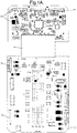
- Figure 1A shows a typical example of an arrangement of two PCBs 1, 2 for use in a junction box according to the prior art.
- the two PCBs 1, 2 are electrically connected by an electrical strap 3.
- the first PCB is the power PCB 1 and has power circuitry 4 mounted on it.
- the second PCB is the signal processing PCB 2 and has signal processing circuitry 5 mounted on it.
- the power PCB 1 of the prior art has generally thicker copper than the signal processing PCB 2 because the power PCB 1 and power circuitry 4 usually drive high currents and the PCB must, therefore, be able to accommodate this.
- An example of the construction of a prior art power PCB 1 might be a PCB having four layers, each having 3oz copper track to help limit the generated heat in the tracks.
- the signal processing circuitry 5 has been mounted on a separate signal processing PCB 2 to the power circuitry 4, as shown in Figure 1A .
- One of the main reasons for this is that it prevents the heat generated by the power circuitry 4 affecting the signal processing circuitry 5.
- Another reason is the difficulty in mounting signal processing circuitry 5 onto track used for power transfer as this track is generally too thick to be able to be formed at a pitch small enough for the pitch of the pins usually found on signal processing circuitry 5.
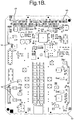
- Figure 1B shows an example of the present invention, a multi-layer PCB 6, having both power circuitry 4 and signal processing circuitry 5 mounted on it for use in a junction box (not shown).
- FR4 dielectric layer is used to construct a multilayer PCB comprising four copper layers. It will be appreciated however that, although FR4 is discussed as being used in this particular example, any suitable PCB dielectric material could be used.
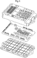
- Figure 2 shows an exploded view of a junction box comprising a single multilayer PCB 6 according to the present invention.
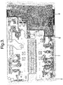
- Figure 3 shows the top surface of the PCB 6 where the power circuitry 4 is mounted on a region having high copper coverage, from hereon called the power region 7, and the signal processing circuitry 5 being mounted on a region of the PCB 6 having low copper coverage, from hereon called the signal processing region 8.
- the two regions 7, 8 are separated by a region of demarcation, which will be referred to from hereon in as a thermal dam 9.
- the thermal dam 9 provides thermal isolation between the two regions 7, 8 and will be explained in more detail later.
- the path of an example thermal dam 9 across a PCB 6 can be seen in Figure 3 , where it separates the power region 7 from the signal processing region 8.
- a further example of a thermal dam 9 is illustrated in Figure 4 , where it can be seen more clearly how a thermal dam 9 may be arranged to separate power circuitry 4 from signal processing circuitry 5.
- the thermal conductivity of copper is approximately 400 W/mK and the thermal conductivity of FR4 dielectric board is approximately 0.23 W/mK. It will be appreciated by a skilled person that the less copper there is present within the thermal dam 9, the less heat will be transferred between the power and signal processing regions 7, 8 through the PCB 6.
- FIG 4 is an illustration of an ideal thermal dam 9, having no copper track on any of the dielectric layers provided within the thermal dam 9.
- a small amount of copper track is provided in at least one of the layers of the thermal dam 9 in order to electrically connect the power circuitry 4 to the signal processing circuitry 5 and to ensure a good level of Electro-Magnetic Compatibility (EMC).
- EMC Electro-Magnetic Compatibility
- the effective thermal conductivity of the power region 7 of the PCB 6 is around 100 W/mK, taking into consideration the combined conductivities of the copper and the FR4 dielectric board.
- the signal processing region 8 has less than half the effective thermal conductivity, at around 10-50 W/mK.
- the effective thermal conductivity of the thermal dam 9, having minimal copper track (comprising only FR4 dielectric board), is around 0.5 W/mK.
- FIG. 4 An example of an arrangement of dielectric layers according to the present invention is shown in Figure 4 , which illustrates an example of a multi-layer PCB 6 having 2oz (70 ⁇ m) copper track 10 on the two outer dielectric layers and 4oz (140 ⁇ m) copper track 12 on the two inner dielectric layers, i.e. a 2-4-4-2 arrangement.
- PCB 6 2oz (70 ⁇ m) copper track 10 on the two outer dielectric layers
- 4oz (140 ⁇ m) copper track 12 on the two inner dielectric layers
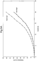
- Figure 5A is a plot of temperature (K) vs. current (A). This chart shows that, for a given current, the temperature of copper track 12 on inner dielectric layers of a multi-layer PCB 6 does not increase as much as the temperature of copper track 10 on outer dielectric layers of the same PCB 6, where the copper track is of the same thickness. This is contrary to standard industry teaching (IPC) as can be seen from the standard industry references shown in Figures 5B and 5C .
- IPC standard industry teaching
- the present invention is arranged such that the tracks that transfer the highest current, and hence have the greatest potential for temperature increase, are arranged on the inner layers.
- Figures 6A and 6B show the advantage of arranging the dielectric layers so that the thicker copper track 12, which carries the highest current, is arranged on the inner dielectric layers.
- the energy (heat) transfer from the top surface of a trace direct to air is the least efficient, air only having a thermal conductivity of 0.024 W/mK.
- the heat transfer from the component trace to air greatly reduces the potential heat transfer possible from the component.
- the present invention makes this desirable arrangement possible by providing a much improved means for dissipating heat from the power circuitry 4 in combination with a new approach to reducing the thermal conductivity between the power region 7 of the PCB 6 and the signal processing region 8 by the inclusion of a thermal dam 9. This has the beneficial effect of preventing the heat generated by the power circuitry 4 from reaching and adversely affecting the performance of the heat sensitive signal processing circuitry 5.
- the much improved means for dissipating heat involves constructing the PCB 6 in a manner that contradicts standard industry teaching (IPC) in the way that its layers are arranged.
- IPC standard industry teaching
- this contradictory arrangement assists the PCB 6 in dissipating heat away from the power circuitry 4 at a rate sufficient to allow the power circuitry 4 to be placed on the same PCB as the signal processing circuitry 5.
- the PCB 6 of the present invention moves away from conventional thinking in that, in contrast to IPC standards, the multi-layer PCB 6 is arranged such that the heavier copper tracks 12 that carry the high power for the circuitry are located on the inner dielectric layers of the PCB. This is because it has been determined that, for a multi-layer PCB having high copper coverage and similar tracks on both the inner and outer dielectric layers, the temperature increase on the inner dielectric layers due to current passing along the tracks will be less than the temperature rise on the outer dielectric layers.
- the 2oz copper track 10 on the outer dielectric layers, with 4oz copper track 12 on the inner dielectric layers (2-4-4-2), arrangement discussed previously is simply one arrangement, which provides the necessary heat dissipation required for a PCB having the particular circuitry used in a junction box. This particular arrangement is considered to allow good heat dissipation whilst keeping the overall copper weight of the PCB 6, and hence cost, to a minimum.
- the thickness of the copper tracks provided on the various dielectric layers of the PCB 6 can be varied according to performance requirements, which could include factors such as budget and the amount of heat being generated by the power circuitry 4.
- copper fill is a technique used on PCBs to extend the life of copper etchant and improve thermal performance.
- a PCB having high copper coverage will have improved thermal performance, in contrast with a PCB having low copper coverage, which will have improved voltage isolation, creepage and clearance performance. It is also important to have a good balance of copper coverage on the surface of a PCB as this facilitates reliable manufacture and improves yield.
- the power region 7 of the PCB is provided with maximum copper fill and hence high copper coverage, whilst the signal processing region 8 of the PCB 6 has minimal copper fill and therefore low copper coverage in comparison.
- the PCB coppercoverage is segmented into regions and provides a thermal dam 9 between the power region 7 and signal processing region 8 on the PCB 6 surface, which has the desirable effect of reducing the thermal conductivity between the power region 7 and the signal processing region 8 of the PCB 6 and hence limiting the amount of heat transferred between the two regions 7, 8.
- the width of the thermal dam 9 separating the power and signal processing regions 7, 8 containing the various power circuitry 4 and signal processing circuitry 5, respectively, can be varied, depending at least on the size requirements of the PCB 6 and the amount of circuitry required to be mounted on it. A skilled person will understand that the wider the thermal dam 9, the better the thermal isolation of the power and signal processing regions 7, 8 from one another.
- FR4 dielectric for the PCB 6
- the dielectric board used is not limited to any one particular type. Indeed, there are numerous types of dielectric board available, having similar properties to FR4, which would be suitable for use with the present invention.
- Track pitch can vary with PCB copper thickness. Due to the PCB etching process, as the copper weight on a layer increases, the differential between the width of a circuitry pad created by its upper (circuitry) edge and the width of its lower (dielectric) edge also increases. The result of this is that as copper weight increases, the minimum distance between circuitry pads (circuitry pin pitch) also increases.
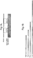
- Figure 7A illustrates the artwork track width/isolation definition and Figure 7B shows examples of the minimum artwork track width and minimum artwork track isolation for different copper weights.
- tracks When tracks are etched on a PCB surface, they are generally trapezoid shaped as a result of the sides of the tracks being etched away. To reliably seat integrated circuit (IC) components onto a track, it is necessary for the track to have a width sufficient to accommodate the pins provided on the IC components for such a purpose.
- IC integrated circuit
- the present invention allows the use of fine pitch components on the outer layers of the PCB 6 for the signal processing circuitry 5.
- thermal conduction it is beneficial for thermal conduction to be able to have the tracks placed closely together on an inner layer of the PCB, as it is desirable to have minimal isolation for good heat spreading.
- the present invention therefore provides a new PCB design technique that targets internal copper layers for high power connections.
- One benefit of this is improved thermal performance, resulting in better heat dissipation, which leads in turn to the PCB 6 and circuitry 4, 5 having a lower temperature rise during operation.
- high copper weight is provided on internal routing layers, with a lower copper weight being provided on the external copper layers.
- the temperature differential between the power region 7 and the signal processing region 8 of the PCB 6 is increased, which allows the signal processing region 8 to be less affected by the potentially high temperature of the power region 7.
- FIG. 1 Another feature of the present invention, which increases the thermal performance of the PCB 6 is that it is provided with thermal vias 11, which are filled with solder.
- Figure 8 illustrates the use of thermal vias 11 to dissipate heat generated by power and signal processing circuitry 4, 5 mounted on a PCB 6 using the copper tracks 10, 12. This is a basic heat transfer principle, which the present invention has improved upon.
- Figure 9 shows an example of solder being introduced to thermal vias by combined reflow and wave soldering techniques, wherein the thermal vias are ideally entirely filled by the solder. Having solder filled thermal vias can improve the thermal performance of the PCB by up to 60%, compared to bare board performance, by reducing thermal resistance through the layers. This in turn results in the power and signal processing circuitry operating at reduced temperatures.
Landscapes
- Engineering & Computer Science (AREA)
- Microelectronics & Electronic Packaging (AREA)
- Production Of Multi-Layered Print Wiring Board (AREA)
- Structure Of Printed Boards (AREA)
Description
- The present invention relates to a junction box. Junction boxes are provided in automotive vehicles as part of their electrical power distribution systems. They distribute electrical power to electrical circuitry via wire harnesses, which generally consist of a plurality of individually insulated wires bunched together, each wire connecting the junction box to electrical circuit, such as an electric motor, a switch or a lamp.
- Modern junction boxes generally contain printed circuit boards (PCB) on which a large number of electronic circuitry are mounted, all of which need to be highly reliable to ensure safe and correct operation of the junction box under all conditions.
- "Smart" junction boxes contain integrated signal processing circuitry, which signal many of the vehicle's functions, for example lighting, windscreen wipers and various sensors. Typical electronic circuitry will comprise switches, connectors, fuses, microcontroller and programmable elements to signal these functions. However, the high sensitivity of such circuitry means that it is very important to ensure that their temperatures are maintained within a safe working range at all times.
- Generally, the smart junction box in an automotive vehicle requires both signal processing circuitry and power circuitry and it would be desirable for both the signal processing circuitry and the power circuitry to be distributed on the same PCB. However, in practice, the signal processing circuitry have had to be mounted on separate PCBs, not only to prevent them being damaged by the high temperatures generated by the power circuitry, but also because of the difficulty in mounting signal processing components, that usually have a fine pitch, on thick PCB tracks used for power transfer.
-
EP-A-1253814 teaches an assembly wherein two inter-connection means are used to connect power and control components: the PCB and the mounting section - An object of the present invention is, therefore, to provide a PCB onto which can be mounted both the signal processing circuitry and the power circuitry, with the heat generated by the power circuitry being prevented from transferring to the signal processing circuitry.
- According to the present invention there is provided a junction box, comprising a multi-layer circuit board, wherein the circuit board comprises: a plurality of dielectric layers comprising at least one inner dielectric layer arranged between at least two outer dielectric layers, each of said dielectric layers having conducting track on a side and arranged one on top of another to form the multi-layered circuit board; power circuitry mounted on the circuit board; signal processing circuitry mounted on the circuit board; and a power input for inputting electrical power into the circuitry on the circuit board, characterised in that: the electrical power is transferred through conducting track arranged to be on an inner dielectric layer, the conducting track on the inner dielectric layer being thicker than the conducting track arranged on the outer dielectric layers, wherein the power circuitry is arranged on one region of the circuit board and the signal processing circuitry is arranged on another region of the circuit board, the two regions being thermally isolated by a thermal dam provided in the circuit board between them.
- There are a number of advantages in enabling both the power circuitry and the signal processing circuitry to be incorporated onto a single PCB. For example, the manufacture of such a PCB requires a simpler production line and process, which results in the board being more reliable because there is less opportunity for errors to be introduced during its manufacture. A single PCB is also a simpler structure, which provides a reduction in weight and expensive materials such as copper, making it more cost effective.
- The present invention suggests an arrangement whereby copper tracks are arranged within a multi-layer PCB in a manner contrary to standard industry teaching (IPC), resulting in a much improved ability of the PCB to dissipate heat away from circuitry whilst allowing for signal processing components to be mounted on the same board as power components.
- For boards with higher copper content, the temperature rise of tracks arranged on inner layers will be lower than the temperature rise of outer tracks having the same track size and the same current. The standard industry teaching actually states the opposite results, which is only true for boards with low copper content. Therefore, in the present invention, the tracks which will dissipate the most heat, which are the tracks carrying the highest currents, are arranged on inner layers.
- By constructing the PCB in this manner, the temperature rise on the power tracks of the PCB is reduced. An example of a PCB according to the present invention would have four layers, with the outer two layers having 70µm (2oz) copper track and the two inner layers having 140µm (4oz) copper track.
- Heat transfer from the power region to the signal processing region on a PCB is further reduced in the present invention by the provision of a region of demarcation between the power region and signal processing region, which acts as a thermal dam, isolating the two regions and thereby reducing the transfer of heat generated by the power circuitry.
- Accordingly, the heat transfer from the power circuitry to the signal processing circuitry can be reduced by an amount sufficient to allow a PCB to contain regions of both power circuitry and signal processing circuitry without the heat created by the power circuitry affecting the signal processing circuitry.
- In addition, plated through holes used as thermal vias may be provided in the PCB, which pass through the layers, thereby allowing heat created by the components fitted on an external copper layer to dissipate to other copper layers (inner and outer). By filling these thermal vias with solder, the present invention has greatly improved the heat dissipation capability of the PCB.
- An example of the present invention will now be described in detail with reference to the accompanying drawings, in which:
-
Figure 1A shows an example of a dual board PCB arrangement previously used in smart junction boxes, whereby the power circuitry are mounted on one PCB and the signal processing circuitry are mounted on a separate PCB, the two PCBs being electrically connected; -
Figure 1B shows an example of a circuit board according to the present invention containing both the power circuitry and the signal processing circuitry; -
Figure 2 shows an exploded view of a junction box comprising a PCB according to the present invention; -
Figure 3 shows the circuit board offigure 1B and the path of a thermal dam which separates the power circuitry and signal processing circuitry regions; -
Figure 4 gives evaluations of the different thermal conductivities of a multilayer PCB carrying both power circuitry and signal processing circuitry, with a thermal dam separating the two regions; -
Figure 5A is a graph illustrating how the temperature rise of copper track on an outer layer of a multilayer PCB compares with the temperature rise of the copper track of same dimension on an inner layer of the same multilayer PCB, for a given current; -
Figure 5B is a chart showing temperature rise for copper track on an outer layer according to standard industry teaching (IPC) data; -
Figure 5C is a chart showing temperature rise for copper track on an inner layer according to standard industry teaching (IPC) data; -
Figure 6A is a cross-section of a multi-layer PCB, illustrating the power dissipation when the power track is on an external layer; -
Figure 6B is a cross-section of a multi-layer PCB, illustrating the power dissipation when the power track is on an internal layer; -
Figures 7A and 7B show how microprocessor pitch can vary with PCB copper thickness/weight; -
Figure 8 illustrates how thermal vias and copper track can be used to dissipate heat generated by circuitry mounted on a board; and -
Figure 9 shows examples of different methods of filling thermal vias with solder to lower the thermal resistance in a PCB. - The invention relates in particular to a printed circuit board (PCB), to be used in "smart" junction boxes (not shown) employed in the automotive industry. The present invention provides a means for being able to accommodate both power and signal processing circuitry on a multi-layer PCB.
-
Figure 1A shows a typical example of an arrangement of twoPCBs PCBs electrical strap 3. The first PCB is thepower PCB 1 and haspower circuitry 4 mounted on it. The second PCB is thesignal processing PCB 2 and hassignal processing circuitry 5 mounted on it. - The
power PCB 1 of the prior art, has generally thicker copper than thesignal processing PCB 2 because thepower PCB 1 andpower circuitry 4 usually drive high currents and the PCB must, therefore, be able to accommodate this. An example of the construction of a priorart power PCB 1 might be a PCB having four layers, each having 3oz copper track to help limit the generated heat in the tracks. - Previously, the
signal processing circuitry 5 has been mounted on a separatesignal processing PCB 2 to thepower circuitry 4, as shown inFigure 1A . One of the main reasons for this is that it prevents the heat generated by thepower circuitry 4 affecting thesignal processing circuitry 5. Another reason is the difficulty in mountingsignal processing circuitry 5 onto track used for power transfer as this track is generally too thick to be able to be formed at a pitch small enough for the pitch of the pins usually found onsignal processing circuitry 5. -
Figure 1B shows an example of the present invention, amulti-layer PCB 6, having bothpower circuitry 4 andsignal processing circuitry 5 mounted on it for use in a junction box (not shown). In this example, FR4 dielectric layer is used to construct a multilayer PCB comprising four copper layers. It will be appreciated however that, although FR4 is discussed as being used in this particular example, any suitable PCB dielectric material could be used. -
Figure 2 shows an exploded view of a junction box comprising asingle multilayer PCB 6 according to the present invention.Figure 3 shows the top surface of thePCB 6 where thepower circuitry 4 is mounted on a region having high copper coverage, from hereon called thepower region 7, and thesignal processing circuitry 5 being mounted on a region of thePCB 6 having low copper coverage, from hereon called thesignal processing region 8. - The two
regions thermal dam 9. Thethermal dam 9 provides thermal isolation between the tworegions thermal dam 9 across aPCB 6 can be seen inFigure 3 , where it separates thepower region 7 from thesignal processing region 8. A further example of athermal dam 9 is illustrated inFigure 4 , where it can be seen more clearly how athermal dam 9 may be arranged to separatepower circuitry 4 fromsignal processing circuitry 5. - The thermal conductivity of copper is approximately 400 W/mK and the thermal conductivity of FR4 dielectric board is approximately 0.23 W/mK. It will be appreciated by a skilled person that the less copper there is present within the
thermal dam 9, the less heat will be transferred between the power andsignal processing regions PCB 6. -
Figure 4 is an illustration of an idealthermal dam 9, having no copper track on any of the dielectric layers provided within thethermal dam 9. In practice, a small amount of copper track is provided in at least one of the layers of thethermal dam 9 in order to electrically connect thepower circuitry 4 to thesignal processing circuitry 5 and to ensure a good level of Electro-Magnetic Compatibility (EMC). - According to an example of the present invention, the effective thermal conductivity of the
power region 7 of thePCB 6 is around 100 W/mK, taking into consideration the combined conductivities of the copper and the FR4 dielectric board. In comparison, thesignal processing region 8 has less than half the effective thermal conductivity, at around 10-50 W/mK. The effective thermal conductivity of thethermal dam 9, having minimal copper track (comprising only FR4 dielectric board), is around 0.5 W/mK. - An example of an arrangement of dielectric layers according to the present invention is shown in
Figure 4 , which illustrates an example of amulti-layer PCB 6 having 2oz (70µm)copper track 10 on the two outer dielectric layers and 4oz (140µm)copper track 12 on the two inner dielectric layers, i.e. a 2-4-4-2 arrangement. Whilst, it will be appreciated that other combinations of copper track thicknesses can be used on the inner and outer dielectric layers, the above example allows for good heat dissipation whilst minimising overall PCB copper weight and, hence, cost. - Considering now the improved heat dissipation aspect of the present invention,
Figure 5A is a plot of temperature (K) vs. current (A). This chart shows that, for a given current, the temperature ofcopper track 12 on inner dielectric layers of amulti-layer PCB 6 does not increase as much as the temperature ofcopper track 10 on outer dielectric layers of thesame PCB 6, where the copper track is of the same thickness. This is contrary to standard industry teaching (IPC) as can be seen from the standard industry references shown inFigures 5B and5C . - Accordingly, since for any given current the temperature rise of an inner dielectric layer is considerably less than that of an outer dielectric layer for a
PCB 6 having high copper coverage, the present invention is arranged such that the tracks that transfer the highest current, and hence have the greatest potential for temperature increase, are arranged on the inner layers. -
Figures 6A and 6B show the advantage of arranging the dielectric layers so that thethicker copper track 12, which carries the highest current, is arranged on the inner dielectric layers. - In the arrangement of
Figure 6A , the energy (heat) transfer from the top surface of a trace direct to air is the least efficient, air only having a thermal conductivity of 0.024 W/mK. The heat transfer from the component trace to air greatly reduces the potential heat transfer possible from the component. - In
Figure 6B , in contrast, the energy transfer (heat) is much more efficient, the heat being transferred away from the PCB trace via the adjacent copper traces and dielectric on all sides, with copper having a thermal conductivity of approximately 400 W/mK, as mentioned before. - One of the reasons it has previously not been possible to mount both the
power circuitry 4 andsignal processing circuitry 5 on thesame PCB 6 was due to the heat generated by thepower circuitry 4 affecting thesignal processing circuitry 5 when in close proximity, as is the case considering a PCB of the size typically required for use in a junction box. - However, as mentioned previously, the present invention makes this desirable arrangement possible by providing a much improved means for dissipating heat from the
power circuitry 4 in combination with a new approach to reducing the thermal conductivity between thepower region 7 of thePCB 6 and thesignal processing region 8 by the inclusion of athermal dam 9. This has the beneficial effect of preventing the heat generated by thepower circuitry 4 from reaching and adversely affecting the performance of the heat sensitivesignal processing circuitry 5. - The much improved means for dissipating heat involves constructing the
PCB 6 in a manner that contradicts standard industry teaching (IPC) in the way that its layers are arranged. However, this contradictory arrangement assists thePCB 6 in dissipating heat away from thepower circuitry 4 at a rate sufficient to allow thepower circuitry 4 to be placed on the same PCB as thesignal processing circuitry 5. - IPC standards, which are the results of industry consensus and collaboration, are respected throughout the whole world and, concerning the construction of multilayer PCBs, it is understood and taught that for a multi-layer PCB having similar tracks on the inner and outer dielectric layers, temperature rise due to current passing along the tracks on the outer dielectric layers will be less than the temperature rise on the inner dielectric layers (see
figures 6B and 6C). However, this has been found to be true only for PCBs with low copper coverage. - The
PCB 6 of the present invention moves away from conventional thinking in that, in contrast to IPC standards, themulti-layer PCB 6 is arranged such that the heavier copper tracks 12 that carry the high power for the circuitry are located on the inner dielectric layers of the PCB. This is because it has been determined that, for a multi-layer PCB having high copper coverage and similar tracks on both the inner and outer dielectric layers, the temperature increase on the inner dielectric layers due to current passing along the tracks will be less than the temperature rise on the outer dielectric layers. - Therefore by placing the high power tracks on the inner dielectric layers of the
PCB 6 it is possible to keep the temperature increases caused by the heat generated by thepower circuitry 4 down to a minimum, with the copper track also acting as very good thermal conductors to dissipate heat away from the circuitry. Of course, it will be appreciated that different thicknesses of copper track can be used in the different dielectric layers of thePCB 6, as long as the basic principle of providing thethicker copper track 12 on the inner dielectric layers is maintained. - The
2oz copper track 10 on the outer dielectric layers, with4oz copper track 12 on the inner dielectric layers (2-4-4-2), arrangement discussed previously is simply one arrangement, which provides the necessary heat dissipation required for a PCB having the particular circuitry used in a junction box. This particular arrangement is considered to allow good heat dissipation whilst keeping the overall copper weight of thePCB 6, and hence cost, to a minimum. - The thickness of the copper tracks provided on the various dielectric layers of the
PCB 6 can be varied according to performance requirements, which could include factors such as budget and the amount of heat being generated by thepower circuitry 4. - Considering now the
thermal dam 9, described above, in more detail, copper fill is a technique used on PCBs to extend the life of copper etchant and improve thermal performance. - Generally, a PCB having high copper coverage will have improved thermal performance, in contrast with a PCB having low copper coverage, which will have improved voltage isolation, creepage and clearance performance. It is also important to have a good balance of copper coverage on the surface of a PCB as this facilitates reliable manufacture and improves yield.
- The
power region 7 of the PCB is provided with maximum copper fill and hence high copper coverage, whilst thesignal processing region 8 of thePCB 6 has minimal copper fill and therefore low copper coverage in comparison. - The PCB coppercoverage is segmented into regions and provides a
thermal dam 9 between thepower region 7 andsignal processing region 8 on thePCB 6 surface, which has the desirable effect of reducing the thermal conductivity between thepower region 7 and thesignal processing region 8 of thePCB 6 and hence limiting the amount of heat transferred between the tworegions - The width of the
thermal dam 9 separating the power andsignal processing regions various power circuitry 4 andsignal processing circuitry 5, respectively, can be varied, depending at least on the size requirements of thePCB 6 and the amount of circuitry required to be mounted on it. A skilled person will understand that the wider thethermal dam 9, the better the thermal isolation of the power andsignal processing regions - Although the preferred embodiment uses FR4 dielectric for the
PCB 6, a skilled person will appreciate that the dielectric board used is not limited to any one particular type. Indeed, there are numerous types of dielectric board available, having similar properties to FR4, which would be suitable for use with the present invention. - Track pitch can vary with PCB copper thickness. Due to the PCB etching process, as the copper weight on a layer increases, the differential between the width of a circuitry pad created by its upper (circuitry) edge and the width of its lower (dielectric) edge also increases. The result of this is that as copper weight increases, the minimum distance between circuitry pads (circuitry pin pitch) also increases.
Figure 7A illustrates the artwork track width/isolation definition andFigure 7B shows examples of the minimum artwork track width and minimum artwork track isolation for different copper weights. - When tracks are etched on a PCB surface, they are generally trapezoid shaped as a result of the sides of the tracks being etched away. To reliably seat integrated circuit (IC) components onto a track, it is necessary for the track to have a width sufficient to accommodate the pins provided on the IC components for such a purpose.
- In particular, when etching high copper weight power tracks, to ensure that there is a suitable mounting surface provided on a pad for an integrated circuit, it is necessary for the base of that pad to be considerably wider than the desired mounting surface. The severity of this effect increases with the PCB copper weight.
- By arranging the
PCB 6 so that the high copper weight power tracks are located on the inner layers, the present invention allows the use of fine pitch components on the outer layers of thePCB 6 for thesignal processing circuitry 5. - If tracks, and hence components, are placed too close together on an outer surface of a PCB, there is a risk that the occurrence of voltage creepage, which increases the closer the tracks are to one another, may affect the PCB performance. However, by having the high power connections arranged on an internal layer, the occurrence of voltage creepage is greatly reduced by the presence of the dielectric on the inner layers.
- Conversely it is beneficial for thermal conduction to be able to have the tracks placed closely together on an inner layer of the PCB, as it is desirable to have minimal isolation for good heat spreading.
- The present invention therefore provides a new PCB design technique that targets internal copper layers for high power connections. One benefit of this is improved thermal performance, resulting in better heat dissipation, which leads in turn to the
PCB 6 andcircuitry - To achieve the desired improved thermal performance, high copper weight is provided on internal routing layers, with a lower copper weight being provided on the external copper layers. This permits integration of
power circuitry 4 and signal processing circuitry on asingle PCB 6, the PCB having improved thermal performance for a given copper weight over prior art designs. - As a result of the improved thermal performance and the copper segregation created by the
signal processing region 8 of the PCB having no copper fill, the temperature differential between thepower region 7 and thesignal processing region 8 of thePCB 6 is increased, which allows thesignal processing region 8 to be less affected by the potentially high temperature of thepower region 7. - Another feature of the present invention, which increases the thermal performance of the
PCB 6 is that it is provided withthermal vias 11, which are filled with solder.Figure 8 illustrates the use ofthermal vias 11 to dissipate heat generated by power andsignal processing circuitry PCB 6 using the copper tracks 10, 12. This is a basic heat transfer principle, which the present invention has improved upon. -
Figure 9 shows an example of solder being introduced to thermal vias by combined reflow and wave soldering techniques, wherein the thermal vias are ideally entirely filled by the solder. Having solder filled thermal vias can improve the thermal performance of the PCB by up to 60%, compared to bare board performance, by reducing thermal resistance through the layers. This in turn results in the power and signal processing circuitry operating at reduced temperatures. - Furthermore, the utilisation of fuses, relays and intelligent MOSFETs result in a relatively small PCB surface region and consequently minimises the overall dimensions of the smart junction box.
Claims (14)
- A junction box, comprising a multi-layer circuit board, wherein the circuit board comprises:a plurality of dielectric layers comprising at least one inner dielectric layer arranged between at least two outer dielectric layers, each of said dielectric layers having a conducting track on a side and arranged one on top of another to form the multi-layered circuit board (6);power circuitry (4) mounted on the circuit board;signal processing circuitry (5) mounted on the circuit board; anda power input for inputting electrical power into the circuitry on the circuit board,wherein the electrical power is transferred through the conducting track (12) arranged on the inner dielectric layer, the conducting track (12) on the inner dielectric layer being thicker than conducting tracks (10) arranged on the outer dielectric layers,wherein the power circuitry is arranged on one region (7) of the circuit board and the signal processing circuitry is arranged on another region (8) of the circuit board, the two regions being thermally isolated by a thermal dam (9) provided in the circuit board between them.
- The junction box according to claim 1, wherein the signal processing circuitry region (8) has a lower copper coverage than the power circuitry region (7).
- The junction box according to claim 1 or 2, wherein the thermal dam (9) passes through all the layers of the circuit board (6).
- The junction box according to claims 1, 2 or 3, wherein electro-magnetic compatibility (EMC) performance is maintained by the presence of a conducting material between the two regions (7, 8) on the circuit board (6).
- The junction box according to claim 4, wherein the thermal dam (9) is a region of dielectric layer containing less than 10% of the conducting material in the power circuitry region (7) of the circuit board (6).
- The junction box according to any preceding claim, wherein the thermal dam (9) on any individual layer has a minimum width of 1 mm.
- The junction box according to claim 6, wherein the circuit board (6) comprises four dielectric layers.
- The junction box according to claim 7, wherein the outer dielectric layers have 70µm conducting track (10) and the inner dielectric layers have 140µm conducting track (12).
- The junction box according to any preceding claim, wherein thermal vias (11) are provided through the multilayer printed circuit board (6), the vias being filled with solder.
- The junction box according to claim 9, wherein the solder is introduced to the vias (11) using a reflow or wave soldering technique, or a combination of both.
- The junction box according to any preceding claim, wherein the power and signal processing circuitry (4, 5) on the printed circuit board (6) comprises any of fuses, relays, MOSFETS, micro-controller and programmable elements.
- The junction box according to any preceding claim, further comprising a programmable element.
- The junction box according to any preceding claim, wherein the power input is a bus bar.
- A junction box for use in an automotive vehicle according to any preceding claim.
Applications Claiming Priority (2)
| Application Number | Priority Date | Filing Date | Title |
|---|---|---|---|
| GB0723213A GB0723213D0 (en) | 2007-11-27 | 2007-11-27 | Junction box |
| PCT/GB2008/003937 WO2009068867A1 (en) | 2007-11-27 | 2008-11-26 | Junction box |
Publications (2)
| Publication Number | Publication Date |
|---|---|
| EP2215899A1 EP2215899A1 (en) | 2010-08-11 |
| EP2215899B1 true EP2215899B1 (en) | 2017-04-12 |
Family
ID=38962202
Family Applications (1)
| Application Number | Title | Priority Date | Filing Date |
|---|---|---|---|
| EP08855250.0A Not-in-force EP2215899B1 (en) | 2007-11-27 | 2008-11-26 | Junction box |
Country Status (5)
| Country | Link |
|---|---|
| US (1) | US9113557B2 (en) |
| EP (1) | EP2215899B1 (en) |
| JP (1) | JP2011505077A (en) |
| GB (1) | GB0723213D0 (en) |
| WO (1) | WO2009068867A1 (en) |
Families Citing this family (9)
| Publication number | Priority date | Publication date | Assignee | Title |
|---|---|---|---|---|
| FR2971666B1 (en) * | 2011-02-10 | 2014-11-14 | Hager Controls | ELECTRICAL CONTROL BLOCK USING PRINTED CIRCUIT TECHNOLOGY FOR POWER LINE DRIVER |
| JP6272648B2 (en) * | 2013-01-30 | 2018-01-31 | 矢崎総業株式会社 | Heat sink-less electronic unit that takes measures against thermal interference |
| US20150036292A1 (en) * | 2013-08-01 | 2015-02-05 | Lear Corporation | Electrical Device for Use in an Automotive Vehicle and Method for Cooling Same |
| US10548213B2 (en) * | 2016-03-07 | 2020-01-28 | Mitsubishi Electric Corporation | Electronic controlling apparatus |
| GB2549128B (en) * | 2016-04-06 | 2019-06-12 | Ge Aviat Systems Ltd | Power control system with improved thermal performance |
| DE102018127075B4 (en) * | 2018-10-30 | 2021-12-30 | Auto-Kabel Management Gmbh | High current circuit |
| FR3104888B1 (en) * | 2019-12-16 | 2023-01-20 | Safran Electrical & Power | Balancing device |
| JP7661862B2 (en) * | 2021-10-04 | 2025-04-15 | 株式会社オートネットワーク技術研究所 | Power supply control device |
| US12081006B2 (en) | 2022-05-30 | 2024-09-03 | Jiangsu Barep Smart Technology Co., Ltd | Junction box mounted to be flush with wall surface and convenient for line repair |
Family Cites Families (13)
| Publication number | Priority date | Publication date | Assignee | Title |
|---|---|---|---|---|
| EP0052738A1 (en) * | 1980-11-25 | 1982-06-02 | Contraves Ag | Circuit board |
| JP3432963B2 (en) * | 1995-06-15 | 2003-08-04 | 沖電気工業株式会社 | Semiconductor integrated circuit |
| JPH1035375A (en) * | 1996-05-22 | 1998-02-10 | Harness Sogo Gijutsu Kenkyusho:Kk | Connectors and electrical connection boxes |
| JPH11307888A (en) * | 1998-04-24 | 1999-11-05 | Furukawa Electric Co Ltd:The | Method of manufacturing circuit board with embedded heat dissipation layer |
| JP2001210786A (en) * | 2000-01-26 | 2001-08-03 | Hitachi Ltd | Semiconductor device and method of manufacturing the same |
| JP3954321B2 (en) * | 2001-04-27 | 2007-08-08 | 矢崎総業株式会社 | Heat conduction prevention structure of electrical junction box |
| JP2002330526A (en) * | 2001-04-27 | 2002-11-15 | Yazaki Corp | Electrical junction box |
| JP2004153142A (en) * | 2002-10-31 | 2004-05-27 | Kubota Corp | Electronic circuit board |
| JP2004327482A (en) * | 2003-04-21 | 2004-11-18 | Fujikura Ltd | Multilayer wiring board, base material for multilayer substrate, and method of manufacturing the same |
| JP2005210044A (en) * | 2003-12-26 | 2005-08-04 | Tdk Corp | Inductor element built-in substrate and power amplifier module |
| KR101107975B1 (en) * | 2004-02-04 | 2012-01-30 | 이비덴 가부시키가이샤 | Multilayer printed wiring board |
| KR100631922B1 (en) * | 2004-02-23 | 2006-10-04 | 삼성전자주식회사 | Multilayer circuit boards with improved heat spreading performance and subsequent manufacturing |
| JP2007019355A (en) * | 2005-07-11 | 2007-01-25 | Hitachi Ltd | Electronic control device and manufacturing method thereof |
-
2007
- 2007-11-27 GB GB0723213A patent/GB0723213D0/en not_active Ceased
-
2008
- 2008-11-26 WO PCT/GB2008/003937 patent/WO2009068867A1/en not_active Ceased
- 2008-11-26 EP EP08855250.0A patent/EP2215899B1/en not_active Not-in-force
- 2008-11-26 US US12/742,365 patent/US9113557B2/en not_active Expired - Fee Related
- 2008-11-26 JP JP2010535448A patent/JP2011505077A/en active Pending
Non-Patent Citations (1)
| Title |
|---|
| None * |
Also Published As
| Publication number | Publication date |
|---|---|
| JP2011505077A (en) | 2011-02-17 |
| GB0723213D0 (en) | 2008-01-09 |
| WO2009068867A1 (en) | 2009-06-04 |
| EP2215899A1 (en) | 2010-08-11 |
| US9113557B2 (en) | 2015-08-18 |
| US20110061930A1 (en) | 2011-03-17 |
Similar Documents
| Publication | Publication Date | Title |
|---|---|---|
| US9113557B2 (en) | Junction box | |
| US9202783B1 (en) | Selective antipad backdrilling for printed circuit boards | |
| US5511306A (en) | Masking of circuit board vias to reduce heat-induced board and chip carrier package warp during wavesolder process | |
| US6646886B1 (en) | Power connection structure | |
| US9839128B2 (en) | Solder void reduction between electronic packages and printed circuit boards | |
| US10028384B2 (en) | Circuit board assembly, control device for a cooler fan module and method | |
| KR102620302B1 (en) | Flexible Printed Circuit Board and Manufacturing Method thereof | |
| CN101107888A (en) | Wired printed circuit board or card comprising conductors with rectangular or square cross-section | |
| ES2943137T3 (en) | high current circuit | |
| JPH04188886A (en) | Printed wiring board | |
| US12225659B2 (en) | Electronic control device | |
| EP4622399A1 (en) | Printed circuit board, electrical circuit assembly and methods of producing a printed circuit board and an electrical circuit assembly | |
| CN104023475A (en) | Printed board, electronic control apparatus and inspection method of printed board | |
| CN115280495A (en) | Power module | |
| JP2008066468A (en) | Circuit material, and on-vehicle electrical connection box storing the same | |
| GB2135521A (en) | Printed circuit boards | |
| CA2679084C (en) | Electronic card and aircraft including same | |
| US10219375B2 (en) | Hybrid circuit assembly | |
| EP2200408B1 (en) | Circuit board device, in particular for an electric power consuming device in a motor vehicle | |
| US10728999B2 (en) | Circuit boards and method to manufacture circuit boards | |
| US20040055782A1 (en) | Surface-mounting type electronic circuit unit having no melting of solder attaching electric part thereto | |
| US20070138632A1 (en) | Electronic carrier board and package structure thereof | |
| US20250247943A1 (en) | Circuit board structure and electric compressor including the same | |
| KR102956629B1 (en) | Circuit Board | |
| US20250294671A1 (en) | Printed circuit board and electronic control device |
Legal Events
| Date | Code | Title | Description |
|---|---|---|---|
| PUAI | Public reference made under article 153(3) epc to a published international application that has entered the european phase |
Free format text: ORIGINAL CODE: 0009012 |
|
| 17P | Request for examination filed |
Effective date: 20100427 |
|
| AK | Designated contracting states |
Kind code of ref document: A1 Designated state(s): AT BE BG CH CY CZ DE DK EE ES FI FR GB GR HR HU IE IS IT LI LT LU LV MC MT NL NO PL PT RO SE SI SK TR |
|
| AX | Request for extension of the european patent |
Extension state: AL BA MK RS |
|
| DAX | Request for extension of the european patent (deleted) | ||
| 17Q | First examination report despatched |
Effective date: 20130117 |
|
| GRAP | Despatch of communication of intention to grant a patent |
Free format text: ORIGINAL CODE: EPIDOSNIGR1 |
|
| INTG | Intention to grant announced |
Effective date: 20161103 |
|
| GRAS | Grant fee paid |
Free format text: ORIGINAL CODE: EPIDOSNIGR3 |
|
| GRAA | (expected) grant |
Free format text: ORIGINAL CODE: 0009210 |
|
| AK | Designated contracting states |
Kind code of ref document: B1 Designated state(s): AT BE BG CH CY CZ DE DK EE ES FI FR GB GR HR HU IE IS IT LI LT LU LV MC MT NL NO PL PT RO SE SI SK TR |
|
| REG | Reference to a national code |
Ref country code: GB Ref legal event code: FG4D |
|
| REG | Reference to a national code |
Ref country code: CH Ref legal event code: EP |
|
| REG | Reference to a national code |
Ref country code: IE Ref legal event code: FG4D |
|
| REG | Reference to a national code |
Ref country code: AT Ref legal event code: REF Ref document number: 884976 Country of ref document: AT Kind code of ref document: T Effective date: 20170515 |
|
| REG | Reference to a national code |
Ref country code: DE Ref legal event code: R096 Ref document number: 602008049767 Country of ref document: DE |
|
| REG | Reference to a national code |
Ref country code: NL Ref legal event code: MP Effective date: 20170412 |
|
| REG | Reference to a national code |
Ref country code: LT Ref legal event code: MG4D |
|
| REG | Reference to a national code |
Ref country code: AT Ref legal event code: MK05 Ref document number: 884976 Country of ref document: AT Kind code of ref document: T Effective date: 20170412 |
|
| PG25 | Lapsed in a contracting state [announced via postgrant information from national office to epo] |
Ref country code: NL Free format text: LAPSE BECAUSE OF FAILURE TO SUBMIT A TRANSLATION OF THE DESCRIPTION OR TO PAY THE FEE WITHIN THE PRESCRIBED TIME-LIMIT Effective date: 20170412 |
|
| REG | Reference to a national code |
Ref country code: FR Ref legal event code: PLFP Year of fee payment: 10 |
|
| PG25 | Lapsed in a contracting state [announced via postgrant information from national office to epo] |
Ref country code: GR Free format text: LAPSE BECAUSE OF FAILURE TO SUBMIT A TRANSLATION OF THE DESCRIPTION OR TO PAY THE FEE WITHIN THE PRESCRIBED TIME-LIMIT Effective date: 20170713 Ref country code: HR Free format text: LAPSE BECAUSE OF FAILURE TO SUBMIT A TRANSLATION OF THE DESCRIPTION OR TO PAY THE FEE WITHIN THE PRESCRIBED TIME-LIMIT Effective date: 20170412 Ref country code: NO Free format text: LAPSE BECAUSE OF FAILURE TO SUBMIT A TRANSLATION OF THE DESCRIPTION OR TO PAY THE FEE WITHIN THE PRESCRIBED TIME-LIMIT Effective date: 20170712 Ref country code: ES Free format text: LAPSE BECAUSE OF FAILURE TO SUBMIT A TRANSLATION OF THE DESCRIPTION OR TO PAY THE FEE WITHIN THE PRESCRIBED TIME-LIMIT Effective date: 20170412 Ref country code: AT Free format text: LAPSE BECAUSE OF FAILURE TO SUBMIT A TRANSLATION OF THE DESCRIPTION OR TO PAY THE FEE WITHIN THE PRESCRIBED TIME-LIMIT Effective date: 20170412 Ref country code: FI Free format text: LAPSE BECAUSE OF FAILURE TO SUBMIT A TRANSLATION OF THE DESCRIPTION OR TO PAY THE FEE WITHIN THE PRESCRIBED TIME-LIMIT Effective date: 20170412 Ref country code: LT Free format text: LAPSE BECAUSE OF FAILURE TO SUBMIT A TRANSLATION OF THE DESCRIPTION OR TO PAY THE FEE WITHIN THE PRESCRIBED TIME-LIMIT Effective date: 20170412 |
|
| PG25 | Lapsed in a contracting state [announced via postgrant information from national office to epo] |
Ref country code: PL Free format text: LAPSE BECAUSE OF FAILURE TO SUBMIT A TRANSLATION OF THE DESCRIPTION OR TO PAY THE FEE WITHIN THE PRESCRIBED TIME-LIMIT Effective date: 20170412 Ref country code: IS Free format text: LAPSE BECAUSE OF FAILURE TO SUBMIT A TRANSLATION OF THE DESCRIPTION OR TO PAY THE FEE WITHIN THE PRESCRIBED TIME-LIMIT Effective date: 20170812 Ref country code: LV Free format text: LAPSE BECAUSE OF FAILURE TO SUBMIT A TRANSLATION OF THE DESCRIPTION OR TO PAY THE FEE WITHIN THE PRESCRIBED TIME-LIMIT Effective date: 20170412 Ref country code: SE Free format text: LAPSE BECAUSE OF FAILURE TO SUBMIT A TRANSLATION OF THE DESCRIPTION OR TO PAY THE FEE WITHIN THE PRESCRIBED TIME-LIMIT Effective date: 20170412 Ref country code: BG Free format text: LAPSE BECAUSE OF FAILURE TO SUBMIT A TRANSLATION OF THE DESCRIPTION OR TO PAY THE FEE WITHIN THE PRESCRIBED TIME-LIMIT Effective date: 20170712 |
|
| REG | Reference to a national code |
Ref country code: DE Ref legal event code: R097 Ref document number: 602008049767 Country of ref document: DE |
|
| PG25 | Lapsed in a contracting state [announced via postgrant information from national office to epo] |
Ref country code: RO Free format text: LAPSE BECAUSE OF FAILURE TO SUBMIT A TRANSLATION OF THE DESCRIPTION OR TO PAY THE FEE WITHIN THE PRESCRIBED TIME-LIMIT Effective date: 20170412 Ref country code: DK Free format text: LAPSE BECAUSE OF FAILURE TO SUBMIT A TRANSLATION OF THE DESCRIPTION OR TO PAY THE FEE WITHIN THE PRESCRIBED TIME-LIMIT Effective date: 20170412 Ref country code: CZ Free format text: LAPSE BECAUSE OF FAILURE TO SUBMIT A TRANSLATION OF THE DESCRIPTION OR TO PAY THE FEE WITHIN THE PRESCRIBED TIME-LIMIT Effective date: 20170412 Ref country code: EE Free format text: LAPSE BECAUSE OF FAILURE TO SUBMIT A TRANSLATION OF THE DESCRIPTION OR TO PAY THE FEE WITHIN THE PRESCRIBED TIME-LIMIT Effective date: 20170412 Ref country code: SK Free format text: LAPSE BECAUSE OF FAILURE TO SUBMIT A TRANSLATION OF THE DESCRIPTION OR TO PAY THE FEE WITHIN THE PRESCRIBED TIME-LIMIT Effective date: 20170412 |
|
| PGFP | Annual fee paid to national office [announced via postgrant information from national office to epo] |
Ref country code: FR Payment date: 20171012 Year of fee payment: 10 Ref country code: DE Payment date: 20171121 Year of fee payment: 10 |
|
| PLBE | No opposition filed within time limit |
Free format text: ORIGINAL CODE: 0009261 |
|
| STAA | Information on the status of an ep patent application or granted ep patent |
Free format text: STATUS: NO OPPOSITION FILED WITHIN TIME LIMIT |
|
| PG25 | Lapsed in a contracting state [announced via postgrant information from national office to epo] |
Ref country code: IT Free format text: LAPSE BECAUSE OF FAILURE TO SUBMIT A TRANSLATION OF THE DESCRIPTION OR TO PAY THE FEE WITHIN THE PRESCRIBED TIME-LIMIT Effective date: 20170412 |
|
| PGFP | Annual fee paid to national office [announced via postgrant information from national office to epo] |
Ref country code: GB Payment date: 20171122 Year of fee payment: 10 |
|
| 26N | No opposition filed |
Effective date: 20180115 |
|
| PG25 | Lapsed in a contracting state [announced via postgrant information from national office to epo] |
Ref country code: SI Free format text: LAPSE BECAUSE OF FAILURE TO SUBMIT A TRANSLATION OF THE DESCRIPTION OR TO PAY THE FEE WITHIN THE PRESCRIBED TIME-LIMIT Effective date: 20170412 |
|
| PG25 | Lapsed in a contracting state [announced via postgrant information from national office to epo] |
Ref country code: MC Free format text: LAPSE BECAUSE OF FAILURE TO SUBMIT A TRANSLATION OF THE DESCRIPTION OR TO PAY THE FEE WITHIN THE PRESCRIBED TIME-LIMIT Effective date: 20170412 |
|
| PG25 | Lapsed in a contracting state [announced via postgrant information from national office to epo] |
Ref country code: CH Free format text: LAPSE BECAUSE OF NON-PAYMENT OF DUE FEES Effective date: 20171130 Ref country code: LI Free format text: LAPSE BECAUSE OF NON-PAYMENT OF DUE FEES Effective date: 20171130 |
|
| PG25 | Lapsed in a contracting state [announced via postgrant information from national office to epo] |
Ref country code: LU Free format text: LAPSE BECAUSE OF NON-PAYMENT OF DUE FEES Effective date: 20171126 |
|
| REG | Reference to a national code |
Ref country code: BE Ref legal event code: MM Effective date: 20171130 |
|
| REG | Reference to a national code |
Ref country code: IE Ref legal event code: MM4A |
|
| PG25 | Lapsed in a contracting state [announced via postgrant information from national office to epo] |
Ref country code: MT Free format text: LAPSE BECAUSE OF NON-PAYMENT OF DUE FEES Effective date: 20171126 |
|
| PG25 | Lapsed in a contracting state [announced via postgrant information from national office to epo] |
Ref country code: IE Free format text: LAPSE BECAUSE OF NON-PAYMENT OF DUE FEES Effective date: 20171126 |
|
| PG25 | Lapsed in a contracting state [announced via postgrant information from national office to epo] |
Ref country code: BE Free format text: LAPSE BECAUSE OF NON-PAYMENT OF DUE FEES Effective date: 20171130 |
|
| REG | Reference to a national code |
Ref country code: DE Ref legal event code: R119 Ref document number: 602008049767 Country of ref document: DE |
|
| PG25 | Lapsed in a contracting state [announced via postgrant information from national office to epo] |
Ref country code: HU Free format text: LAPSE BECAUSE OF FAILURE TO SUBMIT A TRANSLATION OF THE DESCRIPTION OR TO PAY THE FEE WITHIN THE PRESCRIBED TIME-LIMIT; INVALID AB INITIO Effective date: 20081126 |
|
| GBPC | Gb: european patent ceased through non-payment of renewal fee |
Effective date: 20181126 |
|
| PG25 | Lapsed in a contracting state [announced via postgrant information from national office to epo] |
Ref country code: CY Free format text: LAPSE BECAUSE OF NON-PAYMENT OF DUE FEES Effective date: 20170412 Ref country code: DE Free format text: LAPSE BECAUSE OF NON-PAYMENT OF DUE FEES Effective date: 20190601 Ref country code: FR Free format text: LAPSE BECAUSE OF NON-PAYMENT OF DUE FEES Effective date: 20181130 |
|
| PG25 | Lapsed in a contracting state [announced via postgrant information from national office to epo] |
Ref country code: GB Free format text: LAPSE BECAUSE OF NON-PAYMENT OF DUE FEES Effective date: 20181126 |
|
| PG25 | Lapsed in a contracting state [announced via postgrant information from national office to epo] |
Ref country code: TR Free format text: LAPSE BECAUSE OF FAILURE TO SUBMIT A TRANSLATION OF THE DESCRIPTION OR TO PAY THE FEE WITHIN THE PRESCRIBED TIME-LIMIT Effective date: 20170412 |
|
| PG25 | Lapsed in a contracting state [announced via postgrant information from national office to epo] |
Ref country code: PT Free format text: LAPSE BECAUSE OF FAILURE TO SUBMIT A TRANSLATION OF THE DESCRIPTION OR TO PAY THE FEE WITHIN THE PRESCRIBED TIME-LIMIT Effective date: 20170412 |