EP2214205A2 - Elektrooptisches Halbleitermodul und Halbleitermodulschaltung - Google Patents
Elektrooptisches Halbleitermodul und Halbleitermodulschaltung Download PDFInfo
- Publication number
- EP2214205A2 EP2214205A2 EP20100151614 EP10151614A EP2214205A2 EP 2214205 A2 EP2214205 A2 EP 2214205A2 EP 20100151614 EP20100151614 EP 20100151614 EP 10151614 A EP10151614 A EP 10151614A EP 2214205 A2 EP2214205 A2 EP 2214205A2
- Authority
- EP
- European Patent Office
- Prior art keywords
- semiconductor module
- optical
- electro
- chips
- transmitting
- Prior art date
- Legal status (The legal status is an assumption and is not a legal conclusion. Google has not performed a legal analysis and makes no representation as to the accuracy of the status listed.)
- Withdrawn
Links
Images




Classifications
-
- H—ELECTRICITY
- H10—SEMICONDUCTOR DEVICES; ELECTRIC SOLID-STATE DEVICES NOT OTHERWISE PROVIDED FOR
- H10W—GENERIC PACKAGES, INTERCONNECTIONS, CONNECTORS OR OTHER CONSTRUCTIONAL DETAILS OF DEVICES COVERED BY CLASS H10
- H10W90/00—Package configurations
-
- G—PHYSICS
- G02—OPTICS
- G02B—OPTICAL ELEMENTS, SYSTEMS OR APPARATUS
- G02B6/00—Light guides; Structural details of arrangements comprising light guides and other optical elements, e.g. couplings
- G02B6/24—Coupling light guides
- G02B6/42—Coupling light guides with opto-electronic elements
- G02B6/43—Arrangements comprising a plurality of opto-electronic elements and associated optical interconnections
Definitions
- the invention relates to an electro-optical semiconductor module having at least one data communication chip and an electro-optical chip.
- the chips are embedded in a common plastic housing and are electrically connected via connecting elements.
- Such a module is for LED as electro-optical chip from the document US 2006 0022214 A1 known.
- the module includes an LED in an LED housing having an electronic additionally mounted component that controls the light emitted by the LED chip.
- the electronic component is mounted on a substrate adjacent to the LED and may include driver hardware, a network interface, a memory, a processor, a switchable power supply, or other type of electronic component.
- Such constructed modules have the disadvantage that they require a large area of the substrate and thus also require a larger plastic housing to integrate an electronic component such as a kommunikationschip, an electro-optical chip such as an LED chip.
- the object of the invention is to provide a semiconductor module and a semiconductor circuit, which is space-saving and has minimal dimensions. Moreover, it is an object of the invention to open up new ways of data transmission.
- an electro-optical semiconductor module with at least one data communication chip and an electro-optical chip is provided.
- the chips are embedded in a common plastic housing and are electrically connected via connecting elements.
- the electro-optical chip is fixed on the data communication chip.
- the plastic housing has a transmitting and receiving opening, through which optical radiation from and to the electro-optical chip and / or enters.
- This semiconductor module has the advantage that in a confined space, a data communication chip is combined with an electro-optical chip and can exchange and transmit data via optical paths.
- the transmitting and receiving opening to a transparent plastic filling.
- a transparent plastic filling supports the sensitive electro-optical chip and on the other hand it does not hinder the optical radiation at the exit through the transmitting and receiving opening.
- the transmitting and receiving aperture may include a lens system to focus or diffuse the optical beam.
- the transmitting and receiving opening on a surface mounting side of the semiconductor module and to provide ball contacts on this surface mounting side.
- the transmitting and receiving opening should be arranged at least instead of a ball contact position on the surface mounting side.
- This semiconductor module has the advantage that no additional area is required for the transmitting and receiving opening, but rather only a ball contact position is taken up by the transmitting and receiving opening.
- the transmitting and receiving ports may be disposed opposite to the surface mounting side of the semiconductor module.
- the optical radiation will start exactly opposite to the semiconductor module.
- the electro-optical chip is arranged on top and a further electro-optical chip to be arranged on the rear side of the data communication chip and for the semiconductor module to have transmitting and receiving openings both on the surface mounting side and on the opposite side.
- a semiconductor module can be realized, through which an optical path is passed.
- an optical beam in the semiconductor module can be modified and, for example, radiated again to the opposite side.
- a semiconductor module circuit in which a plurality of semiconductor modules according to the preceding variants are arranged on a circuit board with glass fiber reinforcement and optically communicate with each other via the glass fibers of the glass fiber reinforcement.
- a pulse code modulated multiplexed or time-shifted access of the data communication chips via the electro-optical chips is provided on the glass fiber fabric.
- the semiconductor module has a plurality of data communication chips with electro-optical chips and optical transmission and reception openings grouped around a passage window, wherein the data communication chips of the semiconductor module communicate with each other via the electro-optical chips and the transmission and reception openings.
- the transmitting and receiving openings preferably arranged opposite each other in the semiconductor module of a plurality of data communication chips.
- such a semiconductor module has four data communication chips with electro-optical chips, wherein the electro-optical chips and the optical transmission and reception openings are grouped around a rectangular through-window.
- opposite data communication chips of the semiconductor module communicate with one another via the electro-optical chips and the transmission and reception openings.
- Such a module has a cuboid extension and has in its center a data communication window through which, for example, a fiber optic cable can be laid as an optical path.
- the semiconductor module has cooling vanes, on which the data communication chip is mounted, wherein ends of the cooling vanes protrude from the side surfaces of the plastic housing.
- These cooling lugs can be additionally cooled intensively by active cooling via cooling lines, wherein the cooling lines are mechanically connected to the cooling lugs.
- a semiconductor module circuit in which a plurality of semiconductor modules with through-windows are arranged on a circuit board such that a central optical communication path extends through the through windows, and a pulse code modulated multiplexed access of the data communication chips via the electro-optical chips on the central optical communication path is provided.
- Such a semiconductor module circuit has the advantage that a large amount of data can be processed, transported and forwarded in the smallest possible space.
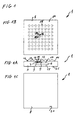
- FIG. 1 shows schematic representations of an electro-optical semiconductor module 1 according to a first embodiment of the invention.
- FIG 1A a cross section through this semiconductor module 1, which is embedded in a plastic housing 8 and on its surface mounting side 14 ball contacts 15 in ball contact positions 16 has.
- a data communication chip 6 is embedded and simultaneously serves as a substrate of an electro-optical chip 7 which is capable of emitting optical signals in the form of optical beams 11.
- the data communication chip 6 has connecting elements 9 on the upper side 17 via which data volumes in the electro-optical chip 7 are transmitted by the data communication chip 6, so that these data quantities can be emitted as optical signals from the electro-optical chip 7 via a transmitting and receiving opening 10.
- the transmitting and receiving opening 10 is provided with a transparent plastic filling 12, so that the electro-optical chip 7 is protected.
- a semiconductor module differs from the prior art in that here a data communication chip 6 is used as a substrate and support for an electro-optical chip 7, whereby advantageously the connecting elements 9 can be significantly shortened and the surface structure of the data communication chip optimally to the structure of Electro-optical chips can be tuned.
- only semiconductor modules are known from the prior art, in which data communication chips are stacked, while in electro-optical semiconductor modules, the electro-optical semiconductor chip is arranged strictly separated from a logic chip or kommunikationschip in a plastic housing, which requires significantly longer connecting elements and makes such semiconductor modules susceptible to interference.
- FIG. 1B shows a plan view of the surface mounting side 14 of the semiconductor module 1, wherein the matrix of the ball contact positions 16, which largely with ball contacts 15th to be moved, can be seen. Only one of the ball contact positions 16 is formed as a transmitting and receiving opening 10, through which an optical coupling of the semiconductor module with other optical components of a semiconductor circuit is possible. In this embodiment of the invention, as already mentioned above, this transmitting and receiving opening 10 is filled with a transparent plastic filling 12.
- Figure 1C shows a plan view of the surface mounting side 14 opposite side 21 of the electro-optical semiconductor module, which remains completely unstructured in this embodiment of the invention and only the outlines of the plastic housing 8 illustrates.
- FIG. 2 shows schematic representations of the electro-optical semiconductor module 1 according to FIG. 1 with laterally arranged cooling vanes 37 and 38.
- These laterally arranged cooling vanes 37 and 38 form a heat sink for the two mutually arranged or stacked chips, wherein the data communication chip 6 is mounted on a thermal bridge 46 with its rear side 18.
- the thermal bridge 46 is thermally connected to the cooling vanes 37 and 38 on the side surfaces 39 of the plastic housing, so that the stack of communication chip 6 and electro-optical chip 7 is intensively cooled.
- FIG. 2B again shows a side 21 of the electro-optical semiconductor module 1, which is opposite to the surface mounting side 14 of the electro-optical semiconductor module 1.
- Figure 2C schematically shows the surface mounting side 14 of the electro-optical semiconductor module 1, which in turn in a ball contact position 16, the transmitting and receiving port 10 of electro-optical semiconductor chips with transparent plastic filling 12 shows.
- FIG. 3 shows schematic representations of an electro-optical semiconductor module 2 according to a second embodiment of the invention.
- Components having the same functions as in the previous figures are identified by the same reference numerals and will not be discussed separately.
- FIG. 3A shows a cross section through the electro-optical semiconductor module 2.
- the electro-optical semiconductor module 2 differs from that in the FIGS. 1 and 2 shown semiconductor module 1 in that this time the electro-optical chip is aligned to the side 21, which is opposite to the surface mounting side 14 of the semiconductor module 2. Consequently, in FIG. 3B no ball contact position 16 is provided for the transmitting and receiving opening, since in this embodiment of the invention, the transmitting and receiving opening 10 is inserted into the side 21, as it FIG. 3C shows.
- FIG. 4 shows schematic representations of the electro-optical semiconductor module 2 according to FIG. 3 with cooling vanes 37 and 38.
- the principle is similar to the first embodiment of the invention.
- the stack of a communication chip 6 and an electro-optical chip 7 can be cooled via the cooling vanes 37 and 38, since the communication chip 6 is arranged on a thermal bridge 46, which is thermally connected to the cooling vanes 37 and 38.
- FIG. 4B Since the electrooptical chip 7 is aligned with the side 21 of the electrooptical semiconductor module 2, FIG FIG. 4B a transmitting and receiving opening 10, while the surface mounting side 14 of FIG. 4C all ball contact positions 16 has occupied with ball contacts.
- FIG. 5 shows schematic representations of an electro-optical semiconductor module 3 according to a third embodiment of the invention.
- Components having the same functions as in the previous figures are identified by the same reference numerals and will not be discussed separately.
- FIG. 5A again shows a cross section through this third embodiment of the invention.
- the difference from the preceding embodiments is that, in addition to the electro-optical semiconductor chip 7 on the upper side 17, a further electro-optical semiconductor chip 20 is arranged on the rear side 18 of the data communication chip 6. This makes it possible to emit optical signals on both sides of the electro-optical semiconductor module.
- an electro-optical transceiver which includes both an optical transmitter and an optical receiver
- optical data can be supplemented by the data communication chip and forwarded as optical signals.
- optical amplifiers that are to be installed in fiber optic lines after finite distances, for example, to amplify an optical incoming signal.
- electro-optical semiconductor module in motor vehicle construction for central control units, as this can increase the interference immunity of such control units.
- both the FIG. 5B on the side 21 of the semiconductor module 3 a transmitting and receiving opening 10 and the figure 5C on the surface mounting side 14, which is equipped with a transmitting and receiving opening 10.
- FIG. 6 shows a schematic cross section through a modification of the electro-optical semiconductor module 1 according to FIG. 1 ,
- the modification is that in this embodiment of the invention, no protective cover of the electro-optical semiconductor chip is provided and the transmitting and receiving opening 10 is kept free of any coating. This is advantageous if the semiconductor module according to FIG. 6 is installed in a housing filled with inert gas.
- FIG. 7 shows a schematic cross section through a further modification of the electro-optical semiconductor module 1 according to FIG. 1 in which a lens system 13 is arranged to focus, for example, the optical radiation 11.
- FIG. 8 shows a schematic cross section through a further modification of the electro-optical semiconductor module 1 according to FIG. 1 , this modification according to FIG. 8 from the modification according to FIG. 6 differs in that in addition cooling tabs 37 and 38 protrude from side surfaces 39 of the electro-optical module 1.
- FIG. 9 shows a schematic cross section through a further modification of the electro-optical semiconductor module 1 according to FIG. 1 This modification is based on the modification according to FIG. 7 differs in that here also on the side surfaces 39 of the semiconductor module 1 from the plastic housing 8 cooling tabs 37 and 38 protrude.
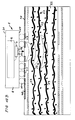
- FIG. 10 shows schematic representations of a semiconductor circuit with an electro-optical semiconductor module 1 according to FIG. 1 on a glass board 23 reinforced circuit board 22nd
- a semiconductor module 1 with a transmitting and receiving opening 10 on the surface mounting side 14 is applied to the circuit board 22 and with corresponding traces of the circuit board, the ball contacts are electrically connected to tracks 48 on respective contact pads 47.
- the electro-optic semiconductor module emits optical signals into the circuit board 22 via the transmitting and receiving aperture 10, these signal sequences are optically transmitted by the glass fibers actually intended to reinforce the circuit board 22 and can be received and evaluated elsewhere on the board ,
- FIG. 10B shows a schematic representation of the semiconductor circuit as in Figure 10A with an electro-optical semiconductor module according to FIG. 1 , wherein the transmitting and receiving opening in the case of the FIG. 10B protected by a transparent plastic filling from damage.
- FIG. 10C shows a further modification of the semiconductor circuit according to Figure 10A in that the transmitting and receiving opening of the semiconductor module on the surface mounting side 14 additionally has a lens system 13 which can focus, focus or scatter the optical radiation.
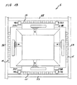
- FIG. 11 shows a schematic perspective view of an electro-optical semiconductor module 4 according to a fourth embodiment of the invention.
- This electro-optical semiconductor module 4 is composed of four electro-optical semiconductor modules 49, 50, 51 and 52 of the second embodiment of the invention.
- These electro-optical semiconductor modules 49 to 52 form a passage window 24, in the transmitting and Reception openings 10 of the electro-optical semiconductor modules 49 to 52 in pairs opposite each other, so that an exchange of data between the individual arranged in a square semiconductor modules 49 to 52 is possible.
- the ball contacts 15 on the surface mounting sides 14 of the assembled to this new electro-optical semiconductor module 4 electro-optic semiconductor modules 49 to 52 are freely accessible.
- FIG. 12 shows a schematic cross section through the electro-optical semiconductor module 4 according to FIG. 11 .
- This cross-section shows the arrangement of the four kommunikationschips 25, 26, 27 and 28 and arranged on the kommunikationschips 25 to 28 electro-optical chips 29 to 32.
- this cross section shows the arrangement of the transmitting and receiving ports 33 to 36, which are arranged in pairs , and the free accessibility of the outwardly disposed ball contacts 15 of the semiconductor modules 49 to 52 according to the second embodiment of the invention.
- FIG. 13 shows a schematic cross section through an electro-optical semiconductor module 5 according to a fifth embodiment of the invention.
- This cross section differs from the cross section according to FIG. 12 in that, in addition to the cooling lugs 37 and 38, further cooling lines 40, 41, 42 and 43 cooperate with the cooling lugs 37 and 38 and thereby intensify the cooling of the semiconductor module 5.
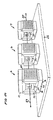
- FIG. 14 shows a schematic representation of a semiconductor circuit on a circuit board 22, on the three aligned electro-optic semiconductor modules 4 of fourth embodiment of the invention are arranged so that the windows 24 of the three electro-optical modules 4 can form an optical path 57, for example by means of a waveguide which is passed through the through-windows 24, in which the transmitting and receiving openings 10 of the electro-optical modules. 4 can couple.
- FIG. 14 thus shows the high flexibility of the solution according to the invention.
Landscapes
- Optical Couplings Of Light Guides (AREA)
Abstract
Die Erfindung betrifft ein elektrooptisches Halbleitermodul (1) mit mindestens einem Datenkommunikationschip (6) und einem elektrooptischen Chip (7). Die Chips (6, 7) sind in einem gemeinsamen Kunststoffgehäuse (8) eingebettet und stehen über Verbindungselemente (9) elektrisch in Verbindung. Der elektrooptische Chip (7) ist auf dem Datenkommunikationschip (8) fixiert. Das Kunststoffgehäuse (8) weist eine Sende- und Empfangsöffnung (10) auf, durch welche optische Strahlung (11) von oder zu dem elektrooptischen Chip (7) aus- und/oder eintritt.
Description
- Die Erfindung betrifft ein elektrooptisches Halbleitermodul mit mindestens einem Datenkommunikationschip und einem elektrooptischen Chip. Die Chips sind in einem gemeinsamen Kunststoffgehäuse eingebettet und stehen über Verbindungselemente elektrisch in Verbindung.
- Ein derartiges Modul ist für LED als elektrooptischer Chip aus der Druckschrift
US 2006 0022214 A1 bekannt. Das Modul enthält eine LED in einem LED-Gehäuse, das eine elektronische zusätzlich montierte Komponente aufweist, die das durch den LED-Chip emittierte Licht steuert. Die elektronische Komponente ist auf einem Substrat neben der LED montiert und kann eine Treiberhardware, eine Netzwerkschnittstelle, einen Speicher, einen Prozessor, eine schaltbare Leistungsversorgung oder eine andere Art einer elektronischen Komponente aufweisen. Derart aufgebaute Module haben den Nachteil, dass sie eine große Fläche des Substrats beanspruchen und damit auch ein größeres Kunststoffgehäuse benötigen, um eine elektronische Komponente wie einen Datenkommunikationschip, einen elektrooptischen Chip wie einen LED-Chip zu integrieren. - Aufgabe der Erfindung ist es, ein Halbleitermodul und eine Halbleiterschaltung zu schaffen, die Raum sparend ist und minimale Dimensionen aufweist. Außerdem ist es Aufgabe der Erfindung, neue Wege der Datenübertragung zu eröffnen.
- Diese Aufgabe wird mit dem Gegenstand der unabhängigen Ansprüche gelöst. Vorteilhafte Weiterbildungen der Erfindung ergeben sich aus den abhängigen Ansprüchen.
- Erfindungsgemäß wird ein elektrooptisches Halbleitermodul mit mindestens einem Datenkommunikationschip und einem elektrooptischen Chip geschaffen. Die Chips sind in einem gemeinsamen Kunststoffgehäuse eingebettet und stehen über Verbindungselemente elektrisch in Verbindung. Der elektrooptische Chip ist auf dem Datenkommunikationschip fixiert. Das Kunststoffgehäuse weist eine Sende- und Empfangsöffnung auf, durch welche optische Strahlung von oder zu dem elektrooptischen Chip aus- und/oder eintritt. Dieses Halbleitermodul hat den Vorteil, dass auf engstem Raum ein Datenkommunikationschip mit einem elektrooptischen Chip kombiniert sind und Daten über optische Pfade austauschen und übertragen können.
- In einer Ausführungsform der Erfindung weist die Sende- und Empfangsöffnung eine transparente Kunststofffüllung auf. Eine derartige transparente Kunststofffüllung stützt einerseits den empfindlichen elektrooptischen Chip und andererseits behindert es die optische Strahlung nicht am Austritt durch die Sende- und Empfangsöffnung. Weiterhin kann die Sende- und Empfangsöffnung ein Linsensystem aufweisen, um den optischen Strahl zu bündeln oder zu streuen.
- In einer weiteren Ausführungsform der Erfindung ist es vorgesehen, die Sende- und Empfangsöffnung auf einer Oberflächenmontageseite des Halbleitermoduls anzuordnen und auf dieser Oberflächenmontageseite Kugelkontakte vorzusehen. Dabei soll die Sende- und Empfangsöffnung mindestens anstelle einer Kugelkontaktposition auf der Oberflächenmontageseite angeordnet werden. Dieses Halbleitermodul hat den Vorteil, dass für die Sende- und Empfangsöffnung keine zusätzliche Fläche erforderlich ist, sondern vielmehr nur eine Kugelkontaktposition durch die Sende- und Empfangsöffnung in Anspruch genommen wird.
- Außerdem kann die Sende- und Empfangsöffnung gegenüberliegend zu der Oberflächenmontageseite des Halbleitermoduls angeordnet sein. In diesem Fall wird die optische Strahlung genau entgegengesetzt von dem Halbleitermodul ausgehen.
- Schließlich ist es vorgesehen, dass der elektrooptische Chip auf der Oberseite und ein weiterer elektrooptischer Chip auf der Rückseite des Datenkommunikationschips angeordnet sind und das Halbleitermodul Sende- und Empfangsöffnungen sowohl zur Oberflächenmontageseite als auch zu der gegenüberliegenden Seite hin aufweist. Damit kann ein Halbleitermodul realisiert werden, durch das ein optischer Pfad hindurchgeführt wird. Jedoch kann durch die Zwischenschaltung des Datenkommunikationsmoduls ein optischer Strahl in dem Halbleitermodul modifiziert und beispielsweise auf die gegenüberliegende Seite wieder abgestrahlt werden.
- Weiterhin ist es vorgesehen, eine Halbleitermodulschaltung zu realisieren, bei der mehrere Halbleitermodule gemäß den vorhergehenden Varianten auf einer Schaltungsplatine mit Glasfaserverstärkung angeordnet sind und über die Glasfasern der Glasfaserverstärkung optisch miteinander kommunizieren. Dabei ist ein pulskodemodulierter multiplexer bzw. zeitversetzter Zugriff der Datenkommunikationschips über die elektrooptischen Chips auf das Glasfasergewebe vorgesehen.
- In einer weiteren Ausführungsform ist es vorgesehen, dass das Halbleitermodul mehrere Datenkommunikationschips mit elektrooptischen Chips und optischen Sende- und Empfangsöffnungen um ein Durchgangsfenster gruppiert aufweist, wobei die Datenkommunikationschips des Halbleitermoduls über die elektrooptischen Chips und die Sende- und Empfangsöffnungen untereinander kommunizieren. Dazu werden die Sende- und Empfangsöffnungen vorzugsweise gegenüberliegend in dem Halbleitermodul aus mehreren Datenkommunikationschips angeordnet.
- Vorzugsweise weist ein derartiges Halbleitermodul vier Datenkommunikationschips mit elektrooptischen Chips auf, wobei die elektrooptischen Chips und die optischen Sende- und Empfangsöffnungen um ein rechtwinkliges Durchgangsfenster gruppiert sind. Dabei kommunizieren gegenüberliegende Datenkommunikationschips des Halbleitermoduls über die elektrooptischen Chips und die Sende- und Empfangsöffnungen miteinander. Ein derartiges Modul hat eine quaderförmige Ausdehnung und weist in seiner Mitte ein Datenkommunikationsfenster auf, durch das beispielsweise eine Glasfaserleitung als optischer Pfad gelegt werden kann.
- Daher ist es vorgesehen, dass das Halbleitermodul Kühlfahnen aufweist, auf denen der Datenkommunikationschip montiert ist, wobei Enden der Kühlfahnen aus den Seitenflächen des Kunststoffgehäuses herausragen. Diese Kühlfahnen können zusätzlich durch aktive Kühlung über Kühlleitungen intensiv gekühlt werden, wobei die Kühlleitungen mit den Kühlfahnen mechanisch verbunden sind.
- Ferner ist es vorgesehen, eine Halbleitermodulschaltung zu realisieren, bei der mehrere Halbleitermodule mit Durchgangsfenster auf einer Schaltungsplatine derart angeordnet sind, dass sich ein zentraler optischer Kommunikationspfad durch die Durchgangsfenster erstreckt, und ein pulskodemodulierter multiplexer bzw. zeitversetzter Zugriff der Datenkommunikationschips über die elektrooptischen Chips auf den zentralen optischen Kommunikationspfad vorgesehen ist. Eine derartige Halbleitermodulschaltung hat den Vorteil, dass eine große Datenmenge auf kleinstem Raum verarbeitet, transportiert und weitergegeben werden kann.
- Die Erfindung wird nun anhand der beigefügten Figuren näher erläutert.
- Figur 1
- zeigt schematische Darstellungen eines elektroopti- schen Halbleitermoduls gemäß einer ersten Ausfüh- rungsform der Erfindung;
- Figur 2
- zeigt schematische Darstellungen des elektroopti- schen Halbleitermoduls gemäß
Figur 1 mit seitlich angeordneten Kühlfahnen; - Figur 3
- zeigt schematische Darstellungen eines elektroopti- schen Halbleitermoduls gemäß einer zweiten Ausfüh- rungsform der Erfindung;
- Figur 4
- zeigt schematische Darstellungen des elektroopti- schen Halbleitermoduls gemäß
Figur 3 mit Kühlfah- nen; - Figur 5
- zeigt schematische Darstellungen eines elektroopti- schen Halbleitermoduls gemäß einer dritten Ausfüh- rungsform der Erfindung;
- Figur 6
- zeigt einen schematischen Querschnitt durch eine Modifikation des elektrooptischen Halbleitermoduls gemäß
Figur 1 ; - Figur 7
- zeigt einen schematischen Querschnitt durch eine weitere Modifikation des elektrooptischen Halblei- termoduls gemäß
Figur 1 ; - Figur 8
- zeigt einen schematischen Querschnitt durch eine weitere Modifikation des elektrooptischen Halblei- termoduls gemäß
Figur 1 ; - Figur 9
- zeigt einen schematischen Querschnitt durch eine weitere Modifikation des elektrooptischen Halblei- termoduls gemäß
Figur 1 ; - Figur 10
- zeigt schematische Darstellungen einer Halbleiter- schaltung eines elektrooptischen Halbleitermoduls gemäß
Figur 1 auf einer glasfaserverstärkten Plati- ne; - Figur 11
- zeigt eine schematische perspektivische Darstellung eines elektrooptischen Halbleitermoduls gemäß einer vierten Ausführungsform der Erfindung;
- Figur 12
- zeigt einen schematischen Querschnitt durch das e- lektrooptische Modul gemäß
Figur 11 ; - Figur 13
- zeigt einen schematischen Querschnitt durch ein e- lektrooptisches Halbleitermodul gemäß einer fünften Ausführungsform der Erfindung;
- Figur 14
- zeigt eine schematische Darstellung einer Halblei- terschaltung auf einer Platine mit elektrooptischen Halbleitermodulen gemäß
Figur 11 . -
Figur 1 zeigt schematische Darstellungen eines elektrooptischen Halbleitermoduls 1 gemäß einer ersten Ausführungsform der Erfindung. - Dabei zeigt
Figur 1A einen Querschnitt durch dieses Halbleitermodul 1, das in ein Kunststoffgehäuse 8 eingebettet ist und auf seiner Oberflächenmontageseite 14 Kugelkontakte 15 in Kugelkontaktpositionen 16 aufweist. In dem Kunststoffgehäuse 8 ist ein Datenkommunikationschip 6 eingebettet und dient gleichzeitig als Substrat eines elektrooptischen Chips 7, der in der Lage ist, optische Signale in Form von optischen Strahlen 11 zu emittieren. Der Datenkommunikationschip 6 weist dazu auf der Oberseite 17 Verbindungselemente 9 auf, über die Datenmengen im elektrooptischen Chip 7 von dem Datenkommunikationschip 6 übertragen werden, so dass diese Datenmengen als optische Signale vom elektrooptischen Chip 7 über eine Sende- und Empfangsöffnung 10 abgestrahlt werden können. - Die Sende- und Empfangsöffnung 10 ist mit einer transparenten Kunststofffüllung 12 versehen, so dass der elektrooptischen Chip 7 geschützt ist. Ein derartiges Halbleitermodul unterscheidet sich von dem Stand der Technik dadurch, dass hier ein Datenkommunikationschip 6 als Substrat und Träger für ein elektrooptisches Chip 7 eingesetzt wird, wodurch in vorteilhafter Weise die Verbindungselemente 9 deutlich verkürzt werden können und die Oberflächenstruktur des Datenkommunikationschips optimal auf die Struktur des elektrooptischen Chips abgestimmt werden kann. Demgegenüber sind aus dem Stand der Technik lediglich Halbleitermodule bekannt, bei denen Datenkommunikationschips aufeinander gestapelt werden, während bei elektrooptischen Halbleitermodulen der elektrooptische Halbleiterchip streng getrennt von einem Logikchip oder Datenkommunikationschip in einem Kunststoffgehäuse angeordnet wird, was deutlich längere Verbindungselemente bedingt und derartige Halbleitermodule störanfälliger macht.
-
Figur 1B zeigt eine Draufsicht auf die Oberflächenmontageseite 14 des Halbleitermoduls 1, wobei die Matrix der Kugelkontaktpositionen 16, die weitestgehend mit Kugelkontakten 15 bewegt werden, zu sehen ist. Nur eine der Kugelkontaktpositionen 16 ist als Sende- und Empfangsöffnung 10 ausgebildet, durch die eine optische Kopplung des Halbleitermoduls mit anderen optischen Komponenten einer Halbleiterschaltung möglich ist. In dieser Ausführungsform der Erfindung ist, wie bereits oben erwähnt, diese Sende- und Empfangsöffnung 10 mit einer transparenten Kunststofffüllung 12 aufgefüllt. -
Figur 1C zeigt eine Draufsicht auf eine der Oberflächenmontageseite 14 gegenüberliegende Seite 21 des elektrooptischen Halbleitermoduls, die bei dieser Ausführungsform der Erfindung vollkommen unstrukturiert bleibt und lediglich die Umrisse des Kunststoffgehäuses 8 verdeutlicht. -
Figur 2 zeigt schematische Darstellungen des elektrooptischen Halbleitermoduls 1 gemäßFigur 1 mit seitlich angeordneten Kühlfahnen 37 und 38. Diese seitlich angeordneten Kühlfahnen 37 und 38 bilden eine Wärmesenke für die beiden aufeinander angeordneten bzw. gestapelten Chips, wobei der Datenkommunikationschip 6 auf einer thermischen Brücke 46 mit seiner Rückseite 18 montiert ist. Die thermische Brücke 46 steht dabei mit den Kühlfahnen 37 und 38 an den Seitenflächen 39 des Kunststoffgehäuses thermisch in Verbindung, so dass der Stapel aus Kommunikationschip 6 und elektrooptischem Chip 7 intensiv gekühlt wird. -
Figur 2B zeigt wiederum eine Seite 21 des elektrooptischen Halbleitermoduls 1, die der Oberflächemontageseite 14 des elektrooptischen Halbleitermoduls 1 gegenüberliegt. -
Figur 2C zeigt schematisch die Oberflächenmontageseite 14 des elektrooptischen Halbleitermoduls 1, die wiederum in einer Kugelkontaktposition 16 die Sende- und Empfangsöffnung 10 des elektrooptischen Halbleiterchips mit transparenter Kunststoffauffüllung 12 zeigt. -
Figur 3 zeigt schematische Darstellungen eines elektrooptischen Halbleitermoduls 2 gemäß einer zweiten Ausführungsform der Erfindung. Komponenten mit gleichen Funktionen wie in den vorhergehenden Figuren werden mit gleichen Bezugszeichen gekennzeichnet und nicht extra erörtert. -
Figur 3A zeigt einen Querschnitt durch das elektrooptische Halbleitermodul 2. Das elektrooptische Halbleitermodul 2 unterscheidet sich von dem in denFiguren 1 und2 gezeigten Halbleitermodul 1 darin, dass diesmal der elektrooptische Chip zu der Seite 21 ausgerichtet ist, die der Oberflächemontageseite 14 des Halbleitermoduls 2 gegenüberliegt. Folglich ist inFigur 3B keine Kugelkontaktposition 16 für die Sende- und Empfangsöffnung vorgesehen, da bei dieser Ausführungsform der Erfindung die Sende- und Empfangsöffnung 10 in die Seite 21 eingebracht ist, wie es dieFigur 3C zeigt. -
Figur 4 zeigt schematische Darstellungen des elektrooptischen Halbleitermoduls 2 gemäßFigur 3 mit Kühlfahnen 37 und 38. Das Prinzip ist ähnlich wie bei der ersten Ausführungsform der Erfindung. Der Stapel aus einem Kommunikationschip 6 und einem elektrooptischen Chip 7 kann über die Kühlfahnen 37 und 38 gekühlt werden, da der Kommunikationschip 6 auf einer thermischen Brücke 46 angeordnet ist, welche mit den Kühlfahnen 37 und 38 thermisch in Verbindung steht. - Da der elektrooptische Chip 7 zu der Seite 21 des elektrooptischen Halbleitermoduls 2 ausgerichtet ist, zeigt die
Figur 4B eine Sende- und Empfangsöffnung 10, während die Oberflächenmontageseite 14 vonFigur 4C sämtliche Kugelkontaktpositionen 16 mit Kugelkontakten belegt hat. -
Figur 5 zeigt schematische Darstellungen eines elektrooptischen Halbleitermoduls 3 gemäß einer dritten Ausführungsform der Erfindung. Komponenten mit gleichen Funktionen wie in den vorhergehenden Figuren werden mit gleichen Bezugszeichen gekennzeichnet und nicht extra erörtert. -
Figur 5A zeigt wiederum einen Querschnitt durch diese dritte Ausführungsform der Erfindung. Der Unterschied zu den vorhergehenden Ausführungsformen besteht darin, dass zusätzlich zu dem elektrooptischen Halbleiterchip 7 auf der Oberseite 17 ein weiterer elektrooptischer Halbleiterchip 20 auf der Rückseite 18 des Datenkommunikationschips 6 angeordnet ist. Damit ist es möglich, zu beiden Seiten des elektrooptischen Halbleitermoduls optische Signale auszusenden. - Wird anstelle von optischen Strahlern wie LED oder Laserdioden ein elektrooptischer Transceiver eingesetzt, der sowohl einen optischen Sender als auch einen optischen Empfänger umfasst, können optische Daten durch den Datenkommunikationschip ergänzt werden und als optische Signale weitergeleitet werden. Dies ist besonders nützlich bei optischen Verstärkern, die beispielsweise in Glasfaserleitungen nach endlichen Entfernungen einzubauen sind, um ein optisches ankommendes Signal verstärkt weiterzugeben. Besonders vorteilhaft ist es jedoch, ein derartiges elektrooptisches Halbleitermodul im Kfz-Bau für zentrale Steuereinheiten einzusetzen, da dadurch die Störsicherheit derartiger Steuereinheiten vergrößert werden kann.
- Aufgrund der beiden elektrooptischen Halbleiterchips 7 und 20 zeigt sowohl die
Figur 5B auf der Seite 21 des Halbleitermoduls 3 eine Sende- und Empfangsöffnung 10 als auch dieFigur 5C auf der Oberflächenmontageseite 14, welche mit einer Sende- und Empfangsöffnung 10 ausgestattet ist. -
Figur 6 zeigt einen schematischen Querschnitt durch eine Modifikation des elektrooptischen Halbleitermoduls 1 gemäßFigur 1 . Die Modifikation besteht darin, dass in dieser Ausführungsform der Erfindung keinerlei Schutzabdeckung des elektrooptischen Halbleiterchips vorgesehen ist und die Sende- und Empfangsöffnung 10 frei von jeder Beschichtung gehalten wird. Dieses ist dann von Vorteil, wenn das Halbleitermodul gemäßFigur 6 in einem mit Inertgas gefüllten Gehäuse eingebaut ist. -
Figur 7 zeigt einen schematischen Querschnitt durch eine weitere Modifikation des elektrooptischen Halbleitermoduls 1 gemäßFigur 1 , bei dem ein Linsensystem 13 angeordnet ist, um beispielsweise die optische Strahlung 11 zu fokussieren. -
Figur 8 zeigt einen schematischen Querschnitt durch eine weitere Modifikation des elektrooptischen Halbleitermoduls 1 gemäßFigur 1 , wobei sich diese Modifikation gemäßFigur 8 von der Modifikation gemäßFigur 6 dadurch unterscheidet, dass zusätzlich Kühlfahnen 37 und 38 aus Seitenflächen 39 des elektrooptischen Moduls 1 herausragen. -
Figur 9 zeigt einen schematischen Querschnitt durch eine weitere Modifikation des elektrooptischen Halbleitermoduls 1 gemäßFigur 1 , wobei diese Modifikation sich von der Modifikation gemäßFigur 7 dadurch unterscheidet, dass auch hier an den Seitenflächen 39 des Halbleitermoduls 1 aus dem Kunststoffgehäuse 8 Kühlfahnen 37 und 38 herausragen. -
Figur 10 zeigt schematische Darstellungen einer Halbleiterschaltung mit einem elektrooptischen Halbleitermodul 1 gemäßFigur 1 auf einer mit Glasfasern 23 verstärkten Schaltungsplatine 22. - In
Figur 10A wird ein Halbleitermodul 1 mit einer Sende- und Empfangsöffnung 10 auf der Oberflächenmontageseite 14 auf die Schaltungsplatine 22 aufgebracht und mit entsprechenden Leiterbahnen der Schaltungsplatine werden die Kugelkontakte auf entsprechenden Kontaktanschlussflächen 47 mit Leiterbahnen 48 elektrisch verbunden. Wenn das elektrooptische Halbleitermodul über die Sende- und Empfangsöffnung 10 optische Signale in die Schaltungsplatine 22 emittiert, so werden diese Signalfolgen von den Glasfasern, die eigentlich zur Verstärkung der Schaltungsplatine 22 vorgesehen sind, optisch übertragen und können an anderen Stellen der Platine empfangen und ausgewertet werden. -
Figur 10B zeigt eine schematische Darstellung der Halbleiterschaltung wie inFigur 10A mit einem elektrooptischen Halbleitermodul gemäßFigur 1 , wobei die Sende- und Empfangsöffnung in dem Fall derFigur 10B durch eine transparente Kunststoffauffüllung vor Beschädigung geschützt ist.Figur 10 C zeigt eine weitere Modifikation der Halbleiterschaltung gemäßFigur 10A , wobei die Sende- und Empfangsöffnung des Halbleitermoduls auf der Oberflächenmontageseite 14 zusätzlich ein Linsensystem 13 aufweist, das die optische Strahlung bündeln, fokussieren oder streuen kann.. -
Figur 11 zeigt eine schematische perspektivische Darstellung eines elektrooptischen Halbleitermoduls 4 gemäß einer vierten Ausführungsform der Erfindung. Dieses elektrooptische Halbleitermodul 4 setzt sich aus vier elektrooptischen Halbleitermodulen 49, 50, 51 und 52 der zweiten Ausführungsform der Erfindung zusammen. Diese elektrooptischen Halbleitermodule 49 bis 52 bilden ein Durchgangsfenster 24, in dem Sende- und Empfangsöffnungen 10 der elektrooptischen Halbleitermodule 49 bis 52 paarweise einander gegenüberliegen, so dass ein Austausch von Daten zwischen den einzelnen derart in einem Viereck angeordneten Halbleitermodulen 49 bis 52 möglich ist. Die Kugelkontakte 15 auf den Oberflächenmontageseiten 14 der zu diesem neuen elektrooptischen Halbleitermodul 4 zusammengestellten elektrooptischen Halbleitermodule 49 bis 52 sind frei zugänglich. -
Figur 12 zeigt einen schematischen Querschnitt durch das elektrooptische Halbleitermodul 4 gemäßFigur 11 . Dieser Querschnitt zeigt die Anordnung der vier Datenkommunikationschips 25, 26, 27 und 28 sowie der auf den Datenkommunikationschips 25 bis 28 angeordneten elektrooptischen Chips 29 bis 32. Außerdem zeigt dieser Querschnitt die Anordnung der Sende- und Empfangsöffnungen 33 bis 36, die paarweise zueinander angeordnet sind, und die freie Zugänglichkeit der nach außen angeordneten Kugelkontakte 15 der Halbleitermodule 49 bis 52 gemäß der zweiten Ausführungsform der Erfindung. -
Figur 13 zeigt einen schematischen Querschnitt durch ein elektrooptisches Halbleitermodul 5 gemäß einer fünften Ausführungsform der Erfindung. Dieser Querschnitt unterscheidet sich von dem Querschnitt gemäßFigur 12 dadurch, dass zusätzlich zu den Kühlfahnen 37 und 38 weitere Kühlleitungen 40, 41, 42 und 43 mit den Kühlfahnen 37 und 38 zusammenwirken und dadurch die Kühlung des Halbleitermoduls 5 intensivieren. Außerdem ist hier schematisch gezeigt, wie beispielsweise die Kugelkontakte 15 auf entsprechenden Schaltungsplatinen 53, 54, 55 und 56 angeordnet werden können. -
Figur 14 zeigt eine schematische Darstellung einer Halbleiterschaltung auf einer Schaltungsplatine 22, auf der drei zueinander ausgerichtete elektrooptische Halbleitermodule 4 der vierten Ausführungsform der Erfindung angeordnet sind, so dass die Fenster 24 der drei elektrooptischen Module 4 einen optischen Pfad 57 beispielsweise mit Hilfe eines Wellenleiters, der durch die Durchgangsfenster 24 hindurchgeführt ist, bilden können, in den die Sende- und Empfangsöffnungen 10 der elektrooptischen Module 4 einkoppeln können.Figur 14 zeigt damit die hohe Flexibilität der erfindungsgemäßen Lösung.
Claims (12)
- Elektrooptisches Halbleitermodul mit mindestens einem Datenkommunikationschip (6) und einem elektrooptischen Chip (7), wobei- die Chips (6, 7) in einem gemeinsamen Kunststoffgehäuse (8) eingebettet sind, und- die Chips (6, 7) über Verbindungselemente (9) elektrisch in Verbindung stehen,dadurch gekennzeichnet, dass der elektrooptische Chip (7) auf dem Datenkommunikationschip (6) fixiert ist und das Kunststoffgehäuse (8) eine Sende- und Empfangsöffnung (10) aufweist, durch welche optische Strahlung (11) von oder zu dem elektrooptischen Chip (7) aus- und/oder eintritt.
- Halbleitermodul nach Anspruch 1, dadurch gekennzeichnet, dass die Sende- und Empfangsöffnung (10) eine transparente Kunststofffüllung (12) aufweist.
- Halbleitermodul nach Anspruch 1 oder Anspruch 2, dadurch gekennzeichnet, dass die Sende- und Empfangsöffnung (10) ein Linsensystem (13) aufweist.
- Halbleitermodul nach einem der vorhergehenden Ansprüche, dadurch gekennzeichnet, dass die Sende- und Empfangsöffnung (10) auf einer Oberflächenmontageseite (14) angeordnet ist, und dass die Oberflächenmontageseite (14) des Halbleitermoduls (1) Kugelkontakte (15) aufweist, und dass die Sende- und Empfangsöffnung (10) mindestens anstelle einer Kugelkontaktposition (16) auf der Oberflächenmontageseite (14) angeordnet ist.
- Halbleitermodul nach einem der vorhergehenden Ansprüche, dadurch gekennzeichnet, dass die Sende- und Empfangsöffnung (10) gegenüberliegend zu einer Oberflächenmontageseite (14) des Halbleitermoduls (1) angeordnet ist.
- Halbleitermodul einem der vorhergehenden Ansprüche, dadurch gekennzeichnet, dass der elektrooptische Chip (7) auf der Oberseite (17) und ein weiterer elektrooptischer Chip (20) auf der Rückseite (18) des Datenkommunikationschips (6) angeordnet sind und das Halbleitermodul (1) Sende- und Empfangsöffnungen (10) zur Oberflächenmontageseite (14) und zu der gegenüberliegenden Seite (21) hin aufweist.
- Halbleitermodulschaltung dadurch gekennzeichnet, dass mehrere Halbleitermodule (1 bis 3) gemäß einem der vorhergehenden Ansprüche auf einer Schaltungsplatine (22) mit Glasfaserverstärkung angeordnet sind und über die Glasfasern (23) der Glasfaserverstärkung optisch miteinander kommunizieren, wobei ein pulskodemodulierter multiplexer bzw. zeitversetzter Zugriff der Datenkommunikationschips (6) über die elektrooptischen Chips (7) auf das Glasfasergewebe vorgesehen ist.
- Halbleitermodul nach einem der Ansprüche 1 bis 6, dadurch gekennzeichnet, dass das Halbleitermodul (1 bis 5) mehrere Datenkommunikationschips (6) mit elektrooptischen Chips (7) und optischen Sende- und Empfangsöffnungen (10) um ein Durchgangsfenster (24) gruppiert aufweist, wobei die Datenkommunikationschips (6) des Halbleitermoduls (1 bis 3) über die elektrooptischen Chips (7) und die Sende- und Empfangsöffnungen (10) untereinander kommunizieren.
- Halbleitermodul nach Anspruch 8, dadurch gekennzeichnet, dass vier Datenkommunikationschips (25 bis 28) mit elektrooptischen Chips (29 bis 32) vorhanden sind, wobei die elektrooptischen Chips und die optischen Sende- und Empfangsöffnungen (33 bis 36) um ein rechtwinkliges Durchgangsfenster (24) gruppiert sind, wobei gegenüberliegende Datenkommunikationschips (25, 27; 26, 28) des Halbleitermoduls (5) über die elektrooptischen Chips (29, 31; 30, 32) und die Sende- und Empfangsöffnungen (33 bis 36) miteinander kommunizieren.
- Halbleitermodul nach Anspruch 8, dadurch gekennzeichnet, dass das Halbleitermodul (1) Kühlfahnen (37, 38) aufweist, auf denen der Datenkommunikationschip (6) montiert ist, wobei Enden der Kühlfahnen (37, 38) aus den Seitenflächen (39) des Kunststoffgehäuses (8) herausragen.
- Halbleitermodul nach Anspruch 10, dadurch gekennzeichnet, dass das Halbleitermodul (1) Kühlleitungen (40 bis 43) aufweist, die als aktive Kühlelemente mit den Kühlfahnen (37, 38) mechanisch verbunden sind.
- Halbleitermodulschaltung, dadurch gekennzeichnet, dass mehrere Halbleitermodule (1 bis 5) gemäß einem der Ansprüche 8 bis 11 mit Durchgangsfenster (24) auf einer Schaltungsplatine (44) derart angeordnet sind, dass sich ein zentraler optischer Kommunikationspfad (45) durch die Durchgangsfenster (24) erstreckt, und ein pulskodemodulierter multiplexer bzw. zeitversetzter Zugriff der Datenkommunikationschips (25 bis 28) über die elektrooptischen Chips (29 bis 32) auf den zentralen optischen Kommunikationspfad (45) vorgesehen ist.
Applications Claiming Priority (1)
| Application Number | Priority Date | Filing Date | Title |
|---|---|---|---|
| DE102009006629A DE102009006629A1 (de) | 2009-01-29 | 2009-01-29 | Elektrooptisches Halbleitermodul und Halbleitermodulschaltung |
Publications (1)
| Publication Number | Publication Date |
|---|---|
| EP2214205A2 true EP2214205A2 (de) | 2010-08-04 |
Family
ID=42224617
Family Applications (1)
| Application Number | Title | Priority Date | Filing Date |
|---|---|---|---|
| EP20100151614 Withdrawn EP2214205A2 (de) | 2009-01-29 | 2010-01-26 | Elektrooptisches Halbleitermodul und Halbleitermodulschaltung |
Country Status (2)
| Country | Link |
|---|---|
| EP (1) | EP2214205A2 (de) |
| DE (1) | DE102009006629A1 (de) |
Citations (1)
| Publication number | Priority date | Publication date | Assignee | Title |
|---|---|---|---|---|
| US20060022214A1 (en) | 2004-07-08 | 2006-02-02 | Color Kinetics, Incorporated | LED package methods and systems |
Family Cites Families (1)
| Publication number | Priority date | Publication date | Assignee | Title |
|---|---|---|---|---|
| DE10332015A1 (de) * | 2003-07-14 | 2005-03-03 | Infineon Technologies Ag | Optoelektronisches Modul mit Senderchip und Verbindungsstück für das Modul zu einer optischen Faser und zu einer Schaltungsplatine, sowie Verfahren zur Herstellung derselben |
-
2009
- 2009-01-29 DE DE102009006629A patent/DE102009006629A1/de not_active Withdrawn
-
2010
- 2010-01-26 EP EP20100151614 patent/EP2214205A2/de not_active Withdrawn
Patent Citations (1)
| Publication number | Priority date | Publication date | Assignee | Title |
|---|---|---|---|---|
| US20060022214A1 (en) | 2004-07-08 | 2006-02-02 | Color Kinetics, Incorporated | LED package methods and systems |
Also Published As
| Publication number | Publication date |
|---|---|
| DE102009006629A1 (de) | 2010-08-19 |
Similar Documents
| Publication | Publication Date | Title |
|---|---|---|
| DE69220540T2 (de) | Optische Verbindungstechniken | |
| DE69937726T2 (de) | Optisches Modul | |
| EP3201663B1 (de) | Optoelektronisches bauelement | |
| DE10238741A1 (de) | Planare optische Komponente und Kopplungsvorrichtung zur Kopplung von Licht zwischen einer planaren optischen Komponente und einem optischen Bauteil | |
| DE112008003784T5 (de) | Flexible, optische Zwischenverbindung | |
| EP0878026B1 (de) | Leuchtdiodenmatrix | |
| DE19826658A1 (de) | Schaltungsträger mit integrierten, aktiven, optischen Funktionen | |
| DE60303140T2 (de) | Optische verbindungsanordnung | |
| DE112008001441B4 (de) | Optische Verbindung | |
| EP0712161B1 (de) | Halbleiterbaugruppe für die bidirektionale, leitungsungebundene, optische Datenübertragung | |
| DE4106721C2 (de) | ||
| DE10121530B4 (de) | Lichtleiteranordnung zur seriellen, bidirektionalen Signalübertragung, optische Leiterplatine und Herstellungsverfahren | |
| DE10121529B4 (de) | Lichtleiteranordnung zur seriellen, bidirektionalen Signalübertragung und optische Leiterplatine | |
| DE4433605A1 (de) | Optischer Transceiver | |
| EP0477177B1 (de) | Koppelelement für lichtwellenleiter | |
| EP0440087B1 (de) | Optische Signalverbindungsvorrichtung für Einschübe eines Einschubgestells | |
| WO2010089254A1 (de) | Elektrooptisches steuer- oder regelgerät und verfahren zum austausch von steuer- oder regelsignalen | |
| DE102009006629A1 (de) | Elektrooptisches Halbleitermodul und Halbleitermodulschaltung | |
| EP1623256B1 (de) | Mikrooptikmodul mit spritzgegossenem gehäuse und verfahren zur herstellung desselben | |
| DE3929794C2 (de) | ||
| DE10160508B4 (de) | Anordnung zur Detektion von optischen Signalen mindestens eines optischen Kanals eines planaren optischen Schaltkreises und/oder zur Einkopplung optischer Signale in mindestens einen optischen Kanal eines planaren optischen Schaltkreises | |
| DE10319900A1 (de) | Optoelektronische Sende- und/oder Empfangsanordnung | |
| EP1447696B1 (de) | Modulares optoelektronisches Bauelement | |
| DE60217861T2 (de) | Optische kommunikationsvorrichtung zwischen elektronischen baugruppen | |
| DE19930418A1 (de) | Lichtwellenleiter-Bussystem, insbesondere für Backplaneanwendungen, mit durch Sternkoppler verbundenen m-Teilnehmern mit jeweils n-Kanälen |
Legal Events
| Date | Code | Title | Description |
|---|---|---|---|
| PUAI | Public reference made under article 153(3) epc to a published international application that has entered the european phase |
Free format text: ORIGINAL CODE: 0009012 |
|
| AK | Designated contracting states |
Kind code of ref document: A2 Designated state(s): AT BE BG CH CY CZ DE DK EE ES FI FR GB GR HR HU IE IS IT LI LT LU LV MC MK MT NL NO PL PT RO SE SI SK SM TR |
|
| AX | Request for extension of the european patent |
Extension state: AL BA RS |
|
| RIC1 | Information provided on ipc code assigned before grant |
Ipc: G02B 6/43 20060101ALN20141217BHEP Ipc: H01L 25/16 20060101AFI20141217BHEP |
|
| STAA | Information on the status of an ep patent application or granted ep patent |
Free format text: STATUS: THE APPLICATION IS DEEMED TO BE WITHDRAWN |
|
| 18D | Application deemed to be withdrawn |
Effective date: 20150801 |