EP2214042B1 - Verfahren zur Herstellung einer photonischen Vorrichtung und entsprechende photonische Vorrichtung - Google Patents
Verfahren zur Herstellung einer photonischen Vorrichtung und entsprechende photonische Vorrichtung Download PDFInfo
- Publication number
- EP2214042B1 EP2214042B1 EP09290077.8A EP09290077A EP2214042B1 EP 2214042 B1 EP2214042 B1 EP 2214042B1 EP 09290077 A EP09290077 A EP 09290077A EP 2214042 B1 EP2214042 B1 EP 2214042B1
- Authority
- EP
- European Patent Office
- Prior art keywords
- layer
- photodetector
- light source
- contact layer
- waveguide
- Prior art date
- Legal status (The legal status is an assumption and is not a legal conclusion. Google has not performed a legal analysis and makes no representation as to the accuracy of the status listed.)
- Not-in-force
Links
Images


Classifications
-
- G—PHYSICS
- G02—OPTICS
- G02B—OPTICAL ELEMENTS, SYSTEMS OR APPARATUS
- G02B6/00—Light guides; Structural details of arrangements comprising light guides and other optical elements, e.g. couplings
- G02B6/24—Coupling light guides
- G02B6/42—Coupling light guides with opto-electronic elements
- G02B6/43—Arrangements comprising a plurality of opto-electronic elements and associated optical interconnections
-
- G—PHYSICS
- G02—OPTICS
- G02B—OPTICAL ELEMENTS, SYSTEMS OR APPARATUS
- G02B6/00—Light guides; Structural details of arrangements comprising light guides and other optical elements, e.g. couplings
- G02B6/10—Light guides; Structural details of arrangements comprising light guides and other optical elements, e.g. couplings of the optical waveguide type
- G02B6/12—Light guides; Structural details of arrangements comprising light guides and other optical elements, e.g. couplings of the optical waveguide type of the integrated circuit kind
- G02B6/13—Integrated optical circuits characterised by the manufacturing method
- G02B6/136—Integrated optical circuits characterised by the manufacturing method by etching
Definitions
- This invention is related to the field of silicon photonics.
- CMOS silicon wafer Complementary Metal Oxide Semiconductor silicon wafer.
- PIC Photonic Integrated Circuit
- silicon into Si02
- CMOS layer CMOS layer
- telecom wavelength comprised between 1,3 and 1,55 ⁇ m.
- silicon has a very poor photon emission efficiency.
- III-V materials known to have very good photon emission and detection efficiencies, on top of the CMOS layers, by means of die to wafer bonding on silicon wafer.
- a reference can be found in G. Roelkens et al., III-V/ Si photonics by die-to-wafer bonding, Materials Todays 2007, vol.10, n° 7-8, pp. 36-43 .
- a typical structure includes a CMOS silicon wafer on the top of which is bonded a die with an active material which, after processing, will define at least one laser and one photodetector.
- the CMOS silicon wafer comprises a stack of a silicon substrate, an oxide buffer layer and a silicon waveguide layer.
- the laser and the photodetector are both made of the same III-V epitaxial layer stack. Therefore, the laser and the photodetector include the same layers.
- a reference can be found in G. Roelkens et al., laser emission and photodetection in a InP/InGaAsP layer integrated on and coupled to a Silicon-on-Insulator waveguide circuit, Optics Express 2006, vol.
- evanescent wave coupling is the process by which electromagnetic waves are transmitted from one medium to another by means of the evanescent, exponentially decaying electromagnetic field.
- the laser generates an electromagnetic field which extends to the underlying waveguide.
- the spatial distribution of the electromagnetic field is such that part of it reaches the waveguide. If the laser and the waveguide are closely located, the evanescent field generated by the laser does not decay much before it reaches the waveguide.
- the drawback of this configuration is that the lasers and photodetectors performances cannot be optimized independently, in terms of layer thickness and composition. Indeed, the same p-i-n structure is used in one area of the die for emission (p-i-n forward biased) and in another area of the die for detection (p-i-n reverse biased).
- this technique cannot be used for some important and common applications where, for instance, a monitoring photodiode has to be implemented in close proximity of a laser, that is to say, at a distance of tens of ⁇ m.
- the invention thus concerns a method of producing a photonic device including at least one light source and at least one photodetector on a structure including a waveguide layer which comprises the following steps:
- This embodiment makes simpler the process according to the invention.
- the shared layer stops the etching in step d).
- a contact layer of the photodetection structure stops the removal of the substrate in step c).
- the substrate can be a III:V substrate.
- the step f) can be obtained by deposition of a layer of an electrical conductor material.
- the invention also relates to a photonic device according to claim 6.
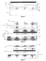
- Figure 1 illustrates the first step of the method according to the invention by showing an epitaxial structure 1 obtained by any suitable process, typically by means of metal organic chemical vapour deposition MOCVD or molecular beam epitaxy MBE techniques.
- the process is carried out on a III-V substrate 10 to obtain first the photodetection p-i-n structure 11 and then the light source or laser n-i-p structure 12. Both structures are stacked.
- the growth is performed on a InP substrate.
- the photodetection structure 11 includes a upper contact layer 110, an absorbing layer 111 and a bottom contact layer 112. As shown in Figure 1 , the photodetector upper contact layer 110 is in the continuation of the substrate 10 and the absorbing layer 111 is located between the upper contact layer 110 and the bottom contact layer 112.
- the light source or laser structure 12 includes an upper contact layer 112, a laser layer 121 and a bottom contact layer 122.
- the thickness of the epitaxy layers is less than 3 ⁇ m when the thickness of the substrate 10 is about 350 ⁇ m.
- photodetector bottom contact layer is also the laser upper contact layer. This reduces the thickness of the epitaxy, and the number of processing steps.
- the structure 1 is then bonded, by means of a die to wafer process for instance, to a SOI wafer 2.
- the SOI wafer 2 includes a Si substrate 20, a layer 21 including a. Si waveguide 210 and a bonding layer 22.
- the structure 2 can be obtained either from:
- the Si waveguide 210 is obtained by hard mask SiOx deposition, photolithography, and etching.
- the waveguide is then covered by SiOx and the surface is planarized by Chemical Mechanical Polishing (CMP) to obtain the bonding layer 22.
- CMP Chemical Mechanical Polishing
- the structure 1 is bonded to the structure 2 in such a way that the laser bottom contact layer 122 is in contact with the bonding layer 22.
- the substrate 10 is then mechanically and chemically removed by any suitable etching process.
- the removal of the substrate can also take place before bonding the structure 1 to the structure 2, but the removal is more difficult to obtain at that stage.
- the photodetector upper contact layer 110 has a composition different from the substrate 10 and thus plays the role of an etch stop layer.
- the structure 3 resulting from this etching is illustrated by figure 3 .
- the photodetector definition can be performed.
- Figure 4 illustrated the resulting structure, which includes the structure 2, the light source or laser structure 12 and a photodetector 4.
- the photodetector comprises a bottom contact layer 42 which is the laser upper contact layer 112, an absorbing layer 41 resulting from layer 111, and an upper contact layer 40 resulting from layer 110.
- the laser geometry can then be defined by dry or wet etching.
- figure 5 which includes the structure 2, the photodetector 4 and the laser 5.
- the laser comprises a bottom contact layer 50 which results from the laser bottom contact layer 122, a laser layer 51 resulting from layer 121, and a upper contact layer 52 resulting from the laser upper contact layer 112.
- the last step of the process according to the invention is illustrated by Figure 6 , and it is an electrode deposition step.
- the electrodes of the photodetector 4 are referenced 43 and 44 while the ones of the laser 5 are referenced 53 and 54.
- Figure 7 illustrates how light is generated, guided, and detected in the complete link (forward bias for the laser, reverse bias for the photodetector).
- the laser is a forward biased p-i-n diode, at a current above the threshold current, in order to obtain the laser effect.
- the light emitted by the laser is coupled in the underlying waveguide (F1), then spreads in the waveguide (F2), and finally is coupled in the photodetector which is a reverse biased p-i-n diode (F3).
- the photodetector upper contact layer 110 can be a 100nm thick highly p-doped In 0.53 Ga 0.47 As (lattice matched to InP) layer which is commonly used to take a p type ohmic contact.
- the etching selectivity between the InP substrate 10 and In 0.53 Ga 0.47 As is extremely high with the etching mixture HCl/H2O, 3/1. Therefore, in the frame of the invention, the In 0.53 Ga 0.47 As layer 110 fulfils two functions: it contributes to the definition of the photodetector, but it also has the function of an etch stop layer during substrate removal.
- the structure 3 after removal of the substrate is illustrated on Figure 3 .
- the absorption layer 111 can be 500nm thick and undoped. It is also made of In 0.53 Ga 0.47 As which has a strong absorption (> 4000cm-1) at telecom wavelength (1.3 ⁇ m-1.55 ⁇ m).
- the photodetector bottom contact layer 112 can be a n doped InP layer which defines the bottom of the photodiode (p-i-n structure) and the top of the laser structure (standard n-i-p structure or tunnel junction n-n + -p + -pi-n structure). It is therefore also the laser upper contact layer.
- a tunnel junction (n + -p + ) structure as shown in Figure 7 , a quaternary material such as InGaAsP (energy gap corresponding to 1.3 ⁇ m) lattice matched to InP is a relevant choice.
- the laser layer 121 can be around 400nm thick and composed of an undoped separate confinement heterostructure (so-called SCH) in which active region such as quantum wells or quantum dots are grown.
- the active layer is composed of either InGaAsP or AlGaInAs-based quaternary compounds.
- the laser bottom contact layer 122 can be made of a ⁇ 200nm thick InP layer which is n doped in the case of a tunnel junction approach or p doped for a standard approach.
- the tunnel junction approach is preferred to couple light efficiently from the laser to the waveguide, since holes absorb more light than electrons (the ratio absorption coefficient of the holes/absorption coefficient of the electrons is 10).
- the photodetector definition can be performed.
- This standard process can be photoresist deposition, photolithography or ebeam lithography, or etching.
- the laser geometry can then be defined by dry etching for instance Reactive Ion Etching with CH 4 /H 2 or Inducely Coupled Plasma etching with Cl 2 /H 2 .
- the light coupling between the waveguide and the photodetector region where light will be absorbed is performed either by an evanescent effect or by a guide to guide effect. These two effects will be described thereafter.
- Figure 8 comprises two curves representing the photodetection efficiency as a function of the photodetector length, and for a thickness of the oxide layer, or bonding layer, taken between the waveguide and the epitaxy layers of 100nm (-) or 200nm (---).
- the simulations were carried out with a laser having a thickness of 500nm and a photodetector made of InGaAs and having also a thickness of 500nm and with Au electrodes.
- Figure 8 shows that the coupling efficiency increases when the length of the detector increases and when the thickness of the bonding layer decreases.
- the detector length is typically in the range 20 ⁇ m - 100 ⁇ m. Some diffraction losses can occur at the interfaces where the photodetector is geometrically defined.
- Figure 8 also shows that, as an example, with a bonding layer having a thickness of 100nm, more than 90% of the light spreading in the waveguide is absorbed in less than 40 ⁇ m.
- the coupling by guide to guide effect is used to increase the compactness of the photodetector. As known by a person skilled in the art, this effect can be obtained with a special design of the waveguides.
- the principle of the device can be understood by referring to Figure 9 .
- the photodetector 4 is provided with a guide to guide coupler 6.
- the width of the coupler is much smaller than the one of the photodetector.
- An adiabatic taper 7 is thus provided in the laser source waveguide between the coupler and the photodetector.
- the coupler and the taper are obtained through additional photolithography steps.
- the light of the silicon waveguide is first transferred in the laser source epilayers by a guide to guide effect.
- the phase matching condition between the silicon and the source waveguide is obtained by a correct choice of the source waveguide width.
- Modeling shows that a width of 0.38 ⁇ m for the source waveguide is necessary to have a coupling efficiency of 100 % between the two waveguides for a silicon waveguide of 0.5 ⁇ m width.
- the performance of the photodetector is almost the same when its operation is based on evanescent coupling or on coupling by guide to guide effect.
- a photodetector as illustrated on Figure 9 presents a higher compactness. For a spacing between the two waveguides of 0.2 ⁇ m, the coupling length is about 8 ⁇ m.
- the light is injected in the photodetector epilayers.
- the depth of the layer stack must be chosen in such a way that the fundamental mode profile of the source epilayers waveguide is matching the first order mode of the waveguide in the layer stack part of the photodetector.
- the size of the photodetector can be reduced to 2 ⁇ m large and 10 ⁇ m long.
- a width of 2 ⁇ m is needed.
- An adiabatic taper in the source waveguide is used to enlarge the width of 0.38 ⁇ m to 2 ⁇ m.
- the total length of the device is about 24 ⁇ m and the length of the photodetector is reduced to 10 ⁇ m.
- the small size of the photodetector will lead to a small capacitance for this device, which should allow for a very high frequency operation for such a photodetection device.
- a photonic device can be obtained in which the performances of the light source(s) and of the photodetector(s) can be optimized independently. Indeed, the layers constituting the light source(s) and the photodetector(s) are realized successively and can be adapted to the expected performances. However, the layers are obtained during the same epitaxy and therefore, the process is not complex.
- the process enables to obtain a photonic device in which the light source(s) and the photodetector(s) can be closely positioned. Indeed, it is not necessary to bond independently the light source(s) and the photodetector(s) on the silicon wafer. Therefore, the minimum distance between the light source(s) and the photodetector is not set by the bonding techniques, but by the lithography resolution. The latter is less than 1 ⁇ m.
- epitaxy can be made simpler by designing the photodetection structure and the light source structure with a shared layer.
- this shared layer is the laser upper contact layer and the photodetector bottom contact layer, referenced 112.
- composition of this shared layer can be chosen so that this layer fulfils the function of an etch stop layer during the process according to the invention. This particular choice also makes the process simpler.
- the etching of the layers 122 and 121 is carried out by plasma-etching and not by chemical etching.
- the photodetector upper contact layer 110 can be chosen in order to stop the removal of the substrate during the process according to the invention. This contributes to the simplification of the process.
- the absorbing layer 111 is the upper layer, it can be selectively removed, anywhere it is necessary to do so. It will not impact the laser performances.
- the absorption coefficient of InGaAs material being high, only a small surface is needed to detect the major part of the light emitted by the laser.
- the photodetector layer can be used as monitoring photo diode for the laser.
- InGaAsP or AlGaInAs alloys can also be used when the photodetector bottom contact layer 112 is a InP layer and GaAsN, InGaAs, InGaAsSb, InGaAsSbN, GaAsSb and GaAsSbN can be used when the photodetector bottom contact layer 112 is a GaAs layer.
- the process according to the invention is thus an interesting way of producing photonic integrated circuits (PIC).
Claims (6)
- Verfahren zum Herstellen einer photonischen Vorrichtung, die mindestens eine Lichtquelle und mindestens einen Photodetektor auf einer Struktur (2) enthält, die eine Wellenleiterschicht (210) enthält, wobei das Verfahren die folgenden Schritte aufweist:a) aufeinanderfolgendes Züchten einer Photoerfassungsstruktur (11) und einer Lichtquellenstruktur (12) auf einem Substrat (10), wobei die Photoerfassungsstruktur und die Lichtquellenstruktur aus einem Stapel von Schichten bestehen, wobei jeder Stapel eine aktive Schicht (111, 121) zwischen zwei Kontaktschichten (110, 112; 112, 122) enthält, wobei die Schichten der Lichtcluellenstruktur oben auf die Schichten der Photoerfassungsstruktur gestapelt sind und beide Strukturen eine dieser Schichten teilen, wobei diese geteilte Schicht eine Kontaktschicht jeder Struktur ist,b) Bonden der Struktur, die durch den Schritt a) erhalten wird, an die Wellenleiterstruktur (2), wobei die Lichtquellenstruktur die Wellenleiterstruktur (2) mittels einer ihrer Kontaktschichten (122) kontaktiert,c) Entfernen des Substrats (10) von der Struktur, die durch den Schritt b) erhalten wird,d) Ätzen der Struktur (3), die durch den Schritt c) erhalten wird, um den mindestens einen Photodetektor (4) zu definieren,e) Ätzen der Struktur, die durch den Schritt d) erhalten wird, um die mindestens eine Lichtquelle (5) zu definieren, so dass die Photodetektorbodenkontaktschicht (42), die näher bei der Wellenleiterstruktur (2) als die aktive Photodetektorschicht (41) ist, dieselbe Struktur wie die obere Lichtquellenkontaktschicht (52) aufweist, die weiter von der Wellenleiterstruktur als die aktive Lichtquellenschicht (51) entfernt ist, wobei die Photodetektorbodenkontaktschicht und die obere Lichtquellenkontaktschicht aus der geteilten Schicht erhalten werden,f) Ausbilden von Elektroden (44, 43; 54, 53) auf dem mindestens einen Photodetektor (4) und der mindestens einen Lichtquelle (5).
- Verfahren nach Anspruch 1, wobei die geteilte Schicht (112) das Ätzen in Schritt d) stoppt.
- Verfahren nach Anspruch 1 oder 2, wobei eine Kontaktschicht (110) der Photoerfassungsstruktur (11) das Entfernen des Substrats (10) in Schritt c) stoppt.
- Verfahren nach einem der Ansprüche 1 bis 3, wobei das Substrat ein III-V-Substrat ist.
- Verfahren nach einem der Ansprüche 1 bis 4, wobei der Schritt f) durch Abscheiden einer Schicht eines elektrischen Leitermaterials erhalten wird.
- Photonische Vorrichtung, die mindestens eine Lichtquelle (5) und mindestens einen Photodetektor (4) auf einer Wellenleiterstruktur (2) enthält, wobei die Wellenleiterstruktur eine Wellenleiterschicht (210) enthält, wobei der Photodetektor und die Lichtquelle aus einem Stapel von Schichten bestehen, wobei jeder Stapel eine aktive Schicht (51, 41) zwischen einer oberen Kontaktschicht (52, 40) und einer Bodenkontaktschicht (50, 42) enthält, wobei die Bodenkontaktschicht näher bei der Wellenleiterstruktur (2) als die jeweilige aktive Schicht (51, 41) ist, wobei die Lichtquellenbodenkontaktschicht (50) die Wellenleiterstruktur (2) kontaktiert, und wobei die obere Lichtquellenkontaktschicht (52) dieselbe Struktur wie die Photodetektorbodenkontaktschicht (42) aufweist und aus einer gezüchteten Schicht erhalten wird, bei der die obere Lichtquellenkontaktschicht und die Photodetektorbodenkontaktschicht vereinigt sind.
Priority Applications (3)
| Application Number | Priority Date | Filing Date | Title |
|---|---|---|---|
| EP09290077.8A EP2214042B1 (de) | 2009-02-02 | 2009-02-02 | Verfahren zur Herstellung einer photonischen Vorrichtung und entsprechende photonische Vorrichtung |
| PCT/IB2010/000414 WO2010086748A1 (en) | 2009-02-02 | 2010-02-01 | Method of producing a photonic device and corresponding photonic device |
| US13/147,015 US8676002B2 (en) | 2009-02-02 | 2010-02-01 | Method of producing a photonic device and corresponding photonic device |
Applications Claiming Priority (1)
| Application Number | Priority Date | Filing Date | Title |
|---|---|---|---|
| EP09290077.8A EP2214042B1 (de) | 2009-02-02 | 2009-02-02 | Verfahren zur Herstellung einer photonischen Vorrichtung und entsprechende photonische Vorrichtung |
Publications (2)
| Publication Number | Publication Date |
|---|---|
| EP2214042A1 EP2214042A1 (de) | 2010-08-04 |
| EP2214042B1 true EP2214042B1 (de) | 2015-03-11 |
Family
ID=40812241
Family Applications (1)
| Application Number | Title | Priority Date | Filing Date |
|---|---|---|---|
| EP09290077.8A Not-in-force EP2214042B1 (de) | 2009-02-02 | 2009-02-02 | Verfahren zur Herstellung einer photonischen Vorrichtung und entsprechende photonische Vorrichtung |
Country Status (3)
| Country | Link |
|---|---|
| US (1) | US8676002B2 (de) |
| EP (1) | EP2214042B1 (de) |
| WO (1) | WO2010086748A1 (de) |
Families Citing this family (15)
| Publication number | Priority date | Publication date | Assignee | Title |
|---|---|---|---|---|
| US9653639B2 (en) * | 2012-02-07 | 2017-05-16 | Apic Corporation | Laser using locally strained germanium on silicon for opto-electronic applications |
| EP2685297B1 (de) * | 2012-07-13 | 2017-12-06 | Huawei Technologies Co., Ltd. | Verfahren zur Herstellung einer photonischen Schaltung mit aktiven und passiven Strukturen |
| JP5758359B2 (ja) | 2012-08-09 | 2015-08-05 | 株式会社東芝 | 光配線デバイスおよびその製造方法 |
| US9322996B2 (en) | 2013-03-07 | 2016-04-26 | Aurrion, Inc. | Simultaneous processing of multiple photonic device layers |
| JP2014215426A (ja) * | 2013-04-25 | 2014-11-17 | 株式会社沖データ | 光電子半導体装置及びその製造方法 |
| US10132957B2 (en) * | 2013-10-22 | 2018-11-20 | Commissariat A L'energie Atomique Et Aux Energies Alternatives | Optomechanical device for actuating and/or detecting movement of a mechanical element, in particular for gravimetric detection |
| WO2015059511A1 (en) | 2013-10-22 | 2015-04-30 | Commissariat à l'énergie atomique et aux énergies alternatives | Optomechanical device with mechanical elements and optical filters for actuating and/or detecting the movement of the elements |
| US11342475B2 (en) * | 2017-08-22 | 2022-05-24 | Rockley Photonics Limited | Schottky photodetector |
| US10461495B2 (en) * | 2018-03-02 | 2019-10-29 | Cisco Technology, Inc. | Substrate technology for quantum dot lasers integrated on silicon |
| US10734788B2 (en) | 2018-03-02 | 2020-08-04 | Cisco Technology, Inc. | Quantum dot lasers integrated on silicon submount with mechanical features and through-silicon vias |
| US10734785B2 (en) | 2018-03-02 | 2020-08-04 | Cisco Technology, Inc. | Silicon photonics co-integrated with quantum dot lasers on silicon |
| WO2020096950A1 (en) * | 2018-11-06 | 2020-05-14 | The Regents Of The University Of California | Heterogeneously integrated indium gallium nitride on silicon photonic integrated circuits |
| US11550099B2 (en) * | 2018-11-21 | 2023-01-10 | The Research Foundation For The State University Of New York | Photonics optoelectrical system |
| TWI829761B (zh) | 2018-11-21 | 2024-01-21 | 紐約州立大學研究基金會 | 具有積體雷射的光學結構 |
| JP7302363B2 (ja) * | 2019-07-31 | 2023-07-04 | 住友電気工業株式会社 | 光半導体素子の製造方法 |
Family Cites Families (5)
| Publication number | Priority date | Publication date | Assignee | Title |
|---|---|---|---|---|
| US6690845B1 (en) * | 1998-10-09 | 2004-02-10 | Fujitsu Limited | Three-dimensional opto-electronic modules with electrical and optical interconnections and methods for making |
| US6706546B2 (en) * | 1998-10-09 | 2004-03-16 | Fujitsu Limited | Optical reflective structures and method for making |
| US7116851B2 (en) * | 2001-10-09 | 2006-10-03 | Infinera Corporation | Optical signal receiver, an associated photonic integrated circuit (RxPIC), and method improving performance |
| CA2463502C (en) * | 2001-10-09 | 2011-09-20 | Infinera Corporation | Digital optical network architecture |
| US20090078963A1 (en) * | 2007-07-09 | 2009-03-26 | Salah Khodja | Nano-optoelectronic chip structure and method |
-
2009
- 2009-02-02 EP EP09290077.8A patent/EP2214042B1/de not_active Not-in-force
-
2010
- 2010-02-01 WO PCT/IB2010/000414 patent/WO2010086748A1/en active Application Filing
- 2010-02-01 US US13/147,015 patent/US8676002B2/en not_active Expired - Fee Related
Also Published As
| Publication number | Publication date |
|---|---|
| US8676002B2 (en) | 2014-03-18 |
| EP2214042A1 (de) | 2010-08-04 |
| WO2010086748A1 (en) | 2010-08-05 |
| US20120063717A1 (en) | 2012-03-15 |
Similar Documents
| Publication | Publication Date | Title |
|---|---|---|
| EP2214042B1 (de) | Verfahren zur Herstellung einer photonischen Vorrichtung und entsprechende photonische Vorrichtung | |
| US8994004B2 (en) | Hybrid silicon optoelectronic device and method of formation | |
| US11550099B2 (en) | Photonics optoelectrical system | |
| KR102059891B1 (ko) | 집적 도파관 커플러 | |
| KR101594467B1 (ko) | 하이브리드 레이저 | |
| US9496435B2 (en) | Microstructure enhanced absorption photosensitive devices | |
| US10476231B2 (en) | Photonic device comprising a laser optically connected to a silicon waveguide and method for manufacturing such a photonic device | |
| US10859764B2 (en) | Integrated active devices with improved optical coupling between active and passive waveguides | |
| US20190288485A1 (en) | Hybrid Silicon Lasers on Bulk Silicon Substrates | |
| JP6300240B2 (ja) | 半導体デバイス | |
| Fedeli et al. | Development of silicon photonics devices using microelectronic tools for the integration on top of a CMOS wafer. | |
| US10641959B1 (en) | Integrated active devices with improved optical coupling to planarized dielectric waveguides | |
| JP2010263153A (ja) | 半導体集積光デバイス及びその作製方法 | |
| Brouckaert et al. | Compact InAlAs–InGaAs metal–semiconductor–metal photodetectors integrated on silicon-on-insulator waveguides | |
| US10700496B2 (en) | Electro-optical device with lateral electron blocking layer | |
| US11209592B2 (en) | Integrated active devices with enhanced optical coupling to dielectric waveguides | |
| CN111987585B (zh) | 一种硅波导输出激光器 | |
| US11719883B1 (en) | Integrated GaAs active devices with improved optical coupling to dielectric waveguides | |
| US20230244034A1 (en) | Active-passive photonic integrated circuit platform | |
| Keyvaninia et al. | Demonstration of a novel III-V-on-Si distributed feedback laser | |
| Sabnis et al. | Intimate monolithic integration of chip-scale photonic circuits | |
| US20230244029A1 (en) | Photonics optoelectrical system | |
| US20240072511A1 (en) | Heterogeneous Integration Using a Germanium Handle Substrate | |
| US11018473B1 (en) | Selective-area growth of III-V materials for integration with silicon photonics | |
| WO2017041812A1 (en) | Optoelectronic device, comprising a waveguide and a semiconductor nanowire array, and method of manufacturing thereof |
Legal Events
| Date | Code | Title | Description |
|---|---|---|---|
| PUAI | Public reference made under article 153(3) epc to a published international application that has entered the european phase |
Free format text: ORIGINAL CODE: 0009012 |
|
| AK | Designated contracting states |
Kind code of ref document: A1 Designated state(s): AT BE BG CH CY CZ DE DK EE ES FI FR GB GR HR HU IE IS IT LI LT LU LV MC MK MT NL NO PL PT RO SE SI SK TR |
|
| AX | Request for extension of the european patent |
Extension state: AL BA RS |
|
| 17P | Request for examination filed |
Effective date: 20100914 |
|
| AKX | Designation fees paid |
Designated state(s): AT BE BG CH CY CZ DE DK EE ES FI FR GB GR HR HU IE IS IT LI LT LU LV MC MK MT NL NO PL PT RO SE SI SK TR |
|
| 17Q | First examination report despatched |
Effective date: 20111104 |
|
| RAP1 | Party data changed (applicant data changed or rights of an application transferred) |
Owner name: INTERUNIVERSITAIR MICRO-ELEKTRONICA CENTRUM VZW Owner name: UNIVERSITE DE GAND Owner name: CENTRE NATIONAL DE LA RECHERCHE SCIENTIFIQUE Owner name: COMMISSARIAT A L'ENERGIE ATOMIQUE ET AUX ENERGIES |
|
| RAP1 | Party data changed (applicant data changed or rights of an application transferred) |
Owner name: UNIVERSITE DE GAND Owner name: INTERUNIVERSITAIR MICRO-ELECTRONICA CENTRUM VZW Owner name: CENTRE NATIONAL DE LA RECHERCHE SCIENTIFIQUE Owner name: COMMISSARIAT A L'ENERGIE ATOMIQUE ET AUX ENERGIES |
|
| RAP1 | Party data changed (applicant data changed or rights of an application transferred) |
Owner name: IMEC Owner name: UNIVERSITEIT GENT Owner name: CENTRE NATIONAL DE LA RECHERCHE SCIENTIFIQUE Owner name: COMMISSARIAT A L'ENERGIE ATOMIQUE ET AUX ENERGIES |
|
| GRAP | Despatch of communication of intention to grant a patent |
Free format text: ORIGINAL CODE: EPIDOSNIGR1 |
|
| RIC1 | Information provided on ipc code assigned before grant |
Ipc: G02B 6/13 20060101ALI20140910BHEP Ipc: G02B 6/43 20060101AFI20140910BHEP Ipc: G02B 6/136 20060101ALI20140910BHEP |
|
| INTG | Intention to grant announced |
Effective date: 20140926 |
|
| GRAS | Grant fee paid |
Free format text: ORIGINAL CODE: EPIDOSNIGR3 |
|
| GRAA | (expected) grant |
Free format text: ORIGINAL CODE: 0009210 |
|
| AK | Designated contracting states |
Kind code of ref document: B1 Designated state(s): AT BE BG CH CY CZ DE DK EE ES FI FR GB GR HR HU IE IS IT LI LT LU LV MC MK MT NL NO PL PT RO SE SI SK TR |
|
| REG | Reference to a national code |
Ref country code: GB Ref legal event code: FG4D |
|
| REG | Reference to a national code |
Ref country code: CH Ref legal event code: EP |
|
| REG | Reference to a national code |
Ref country code: IE Ref legal event code: FG4D |
|
| REG | Reference to a national code |
Ref country code: AT Ref legal event code: REF Ref document number: 715650 Country of ref document: AT Kind code of ref document: T Effective date: 20150415 |
|
| REG | Reference to a national code |
Ref country code: DE Ref legal event code: R096 Ref document number: 602009029913 Country of ref document: DE Effective date: 20150423 |
|
| REG | Reference to a national code |
Ref country code: NL Ref legal event code: VDEP Effective date: 20150311 |
|
| REG | Reference to a national code |
Ref country code: NL Ref legal event code: VDEP Effective date: 20150311 |
|
| PG25 | Lapsed in a contracting state [announced via postgrant information from national office to epo] |
Ref country code: FI Free format text: LAPSE BECAUSE OF FAILURE TO SUBMIT A TRANSLATION OF THE DESCRIPTION OR TO PAY THE FEE WITHIN THE PRESCRIBED TIME-LIMIT Effective date: 20150311 Ref country code: LT Free format text: LAPSE BECAUSE OF FAILURE TO SUBMIT A TRANSLATION OF THE DESCRIPTION OR TO PAY THE FEE WITHIN THE PRESCRIBED TIME-LIMIT Effective date: 20150311 Ref country code: ES Free format text: LAPSE BECAUSE OF FAILURE TO SUBMIT A TRANSLATION OF THE DESCRIPTION OR TO PAY THE FEE WITHIN THE PRESCRIBED TIME-LIMIT Effective date: 20150311 Ref country code: NO Free format text: LAPSE BECAUSE OF FAILURE TO SUBMIT A TRANSLATION OF THE DESCRIPTION OR TO PAY THE FEE WITHIN THE PRESCRIBED TIME-LIMIT Effective date: 20150611 Ref country code: HR Free format text: LAPSE BECAUSE OF FAILURE TO SUBMIT A TRANSLATION OF THE DESCRIPTION OR TO PAY THE FEE WITHIN THE PRESCRIBED TIME-LIMIT Effective date: 20150311 Ref country code: SE Free format text: LAPSE BECAUSE OF FAILURE TO SUBMIT A TRANSLATION OF THE DESCRIPTION OR TO PAY THE FEE WITHIN THE PRESCRIBED TIME-LIMIT Effective date: 20150311 |
|
| REG | Reference to a national code |
Ref country code: AT Ref legal event code: MK05 Ref document number: 715650 Country of ref document: AT Kind code of ref document: T Effective date: 20150311 |
|
| REG | Reference to a national code |
Ref country code: LT Ref legal event code: MG4D |
|
| PG25 | Lapsed in a contracting state [announced via postgrant information from national office to epo] |
Ref country code: LV Free format text: LAPSE BECAUSE OF FAILURE TO SUBMIT A TRANSLATION OF THE DESCRIPTION OR TO PAY THE FEE WITHIN THE PRESCRIBED TIME-LIMIT Effective date: 20150311 Ref country code: GR Free format text: LAPSE BECAUSE OF FAILURE TO SUBMIT A TRANSLATION OF THE DESCRIPTION OR TO PAY THE FEE WITHIN THE PRESCRIBED TIME-LIMIT Effective date: 20150612 |
|
| PG25 | Lapsed in a contracting state [announced via postgrant information from national office to epo] |
Ref country code: NL Free format text: LAPSE BECAUSE OF FAILURE TO SUBMIT A TRANSLATION OF THE DESCRIPTION OR TO PAY THE FEE WITHIN THE PRESCRIBED TIME-LIMIT Effective date: 20150311 |
|
| PG25 | Lapsed in a contracting state [announced via postgrant information from national office to epo] |
Ref country code: SK Free format text: LAPSE BECAUSE OF FAILURE TO SUBMIT A TRANSLATION OF THE DESCRIPTION OR TO PAY THE FEE WITHIN THE PRESCRIBED TIME-LIMIT Effective date: 20150311 Ref country code: CZ Free format text: LAPSE BECAUSE OF FAILURE TO SUBMIT A TRANSLATION OF THE DESCRIPTION OR TO PAY THE FEE WITHIN THE PRESCRIBED TIME-LIMIT Effective date: 20150311 Ref country code: RO Free format text: LAPSE BECAUSE OF FAILURE TO SUBMIT A TRANSLATION OF THE DESCRIPTION OR TO PAY THE FEE WITHIN THE PRESCRIBED TIME-LIMIT Effective date: 20150311 Ref country code: PT Free format text: LAPSE BECAUSE OF FAILURE TO SUBMIT A TRANSLATION OF THE DESCRIPTION OR TO PAY THE FEE WITHIN THE PRESCRIBED TIME-LIMIT Effective date: 20150713 Ref country code: EE Free format text: LAPSE BECAUSE OF FAILURE TO SUBMIT A TRANSLATION OF THE DESCRIPTION OR TO PAY THE FEE WITHIN THE PRESCRIBED TIME-LIMIT Effective date: 20150311 |
|
| PG25 | Lapsed in a contracting state [announced via postgrant information from national office to epo] |
Ref country code: IS Free format text: LAPSE BECAUSE OF FAILURE TO SUBMIT A TRANSLATION OF THE DESCRIPTION OR TO PAY THE FEE WITHIN THE PRESCRIBED TIME-LIMIT Effective date: 20150711 Ref country code: PL Free format text: LAPSE BECAUSE OF FAILURE TO SUBMIT A TRANSLATION OF THE DESCRIPTION OR TO PAY THE FEE WITHIN THE PRESCRIBED TIME-LIMIT Effective date: 20150311 Ref country code: AT Free format text: LAPSE BECAUSE OF FAILURE TO SUBMIT A TRANSLATION OF THE DESCRIPTION OR TO PAY THE FEE WITHIN THE PRESCRIBED TIME-LIMIT Effective date: 20150311 |
|
| REG | Reference to a national code |
Ref country code: DE Ref legal event code: R097 Ref document number: 602009029913 Country of ref document: DE |
|
| PG25 | Lapsed in a contracting state [announced via postgrant information from national office to epo] |
Ref country code: IT Free format text: LAPSE BECAUSE OF FAILURE TO SUBMIT A TRANSLATION OF THE DESCRIPTION OR TO PAY THE FEE WITHIN THE PRESCRIBED TIME-LIMIT Effective date: 20150311 |
|
| PLBE | No opposition filed within time limit |
Free format text: ORIGINAL CODE: 0009261 |
|
| STAA | Information on the status of an ep patent application or granted ep patent |
Free format text: STATUS: NO OPPOSITION FILED WITHIN TIME LIMIT |
|
| PG25 | Lapsed in a contracting state [announced via postgrant information from national office to epo] |
Ref country code: DK Free format text: LAPSE BECAUSE OF FAILURE TO SUBMIT A TRANSLATION OF THE DESCRIPTION OR TO PAY THE FEE WITHIN THE PRESCRIBED TIME-LIMIT Effective date: 20150311 |
|
| 26N | No opposition filed |
Effective date: 20151214 |
|
| PG25 | Lapsed in a contracting state [announced via postgrant information from national office to epo] |
Ref country code: SI Free format text: LAPSE BECAUSE OF FAILURE TO SUBMIT A TRANSLATION OF THE DESCRIPTION OR TO PAY THE FEE WITHIN THE PRESCRIBED TIME-LIMIT Effective date: 20150311 |
|
| REG | Reference to a national code |
Ref country code: FR Ref legal event code: PLFP Year of fee payment: 8 |
|
| PG25 | Lapsed in a contracting state [announced via postgrant information from national office to epo] |
Ref country code: BE Free format text: LAPSE BECAUSE OF NON-PAYMENT OF DUE FEES Effective date: 20160229 |
|
| PG25 | Lapsed in a contracting state [announced via postgrant information from national office to epo] |
Ref country code: BE Free format text: LAPSE BECAUSE OF FAILURE TO SUBMIT A TRANSLATION OF THE DESCRIPTION OR TO PAY THE FEE WITHIN THE PRESCRIBED TIME-LIMIT Effective date: 20150311 |
|
| PG25 | Lapsed in a contracting state [announced via postgrant information from national office to epo] |
Ref country code: LU Free format text: LAPSE BECAUSE OF FAILURE TO SUBMIT A TRANSLATION OF THE DESCRIPTION OR TO PAY THE FEE WITHIN THE PRESCRIBED TIME-LIMIT Effective date: 20160202 Ref country code: MC Free format text: LAPSE BECAUSE OF FAILURE TO SUBMIT A TRANSLATION OF THE DESCRIPTION OR TO PAY THE FEE WITHIN THE PRESCRIBED TIME-LIMIT Effective date: 20150311 |
|
| REG | Reference to a national code |
Ref country code: CH Ref legal event code: PL |
|
| PG25 | Lapsed in a contracting state [announced via postgrant information from national office to epo] |
Ref country code: CH Free format text: LAPSE BECAUSE OF NON-PAYMENT OF DUE FEES Effective date: 20160229 Ref country code: LI Free format text: LAPSE BECAUSE OF NON-PAYMENT OF DUE FEES Effective date: 20160229 |
|
| REG | Reference to a national code |
Ref country code: IE Ref legal event code: MM4A |
|
| PG25 | Lapsed in a contracting state [announced via postgrant information from national office to epo] |
Ref country code: IE Free format text: LAPSE BECAUSE OF NON-PAYMENT OF DUE FEES Effective date: 20160202 |
|
| REG | Reference to a national code |
Ref country code: FR Ref legal event code: PLFP Year of fee payment: 9 |
|
| PG25 | Lapsed in a contracting state [announced via postgrant information from national office to epo] |
Ref country code: MT Free format text: LAPSE BECAUSE OF FAILURE TO SUBMIT A TRANSLATION OF THE DESCRIPTION OR TO PAY THE FEE WITHIN THE PRESCRIBED TIME-LIMIT Effective date: 20150311 |
|
| REG | Reference to a national code |
Ref country code: FR Ref legal event code: PLFP Year of fee payment: 10 |
|
| PG25 | Lapsed in a contracting state [announced via postgrant information from national office to epo] |
Ref country code: HU Free format text: LAPSE BECAUSE OF FAILURE TO SUBMIT A TRANSLATION OF THE DESCRIPTION OR TO PAY THE FEE WITHIN THE PRESCRIBED TIME-LIMIT; INVALID AB INITIO Effective date: 20090202 Ref country code: CY Free format text: LAPSE BECAUSE OF FAILURE TO SUBMIT A TRANSLATION OF THE DESCRIPTION OR TO PAY THE FEE WITHIN THE PRESCRIBED TIME-LIMIT Effective date: 20150311 |
|
| PG25 | Lapsed in a contracting state [announced via postgrant information from national office to epo] |
Ref country code: MK Free format text: LAPSE BECAUSE OF FAILURE TO SUBMIT A TRANSLATION OF THE DESCRIPTION OR TO PAY THE FEE WITHIN THE PRESCRIBED TIME-LIMIT Effective date: 20150311 Ref country code: MT Free format text: LAPSE BECAUSE OF FAILURE TO SUBMIT A TRANSLATION OF THE DESCRIPTION OR TO PAY THE FEE WITHIN THE PRESCRIBED TIME-LIMIT Effective date: 20160229 Ref country code: TR Free format text: LAPSE BECAUSE OF FAILURE TO SUBMIT A TRANSLATION OF THE DESCRIPTION OR TO PAY THE FEE WITHIN THE PRESCRIBED TIME-LIMIT Effective date: 20150311 |
|
| PG25 | Lapsed in a contracting state [announced via postgrant information from national office to epo] |
Ref country code: BG Free format text: LAPSE BECAUSE OF FAILURE TO SUBMIT A TRANSLATION OF THE DESCRIPTION OR TO PAY THE FEE WITHIN THE PRESCRIBED TIME-LIMIT Effective date: 20150311 |
|
| PGFP | Annual fee paid to national office [announced via postgrant information from national office to epo] |
Ref country code: FR Payment date: 20210226 Year of fee payment: 13 |
|
| PGFP | Annual fee paid to national office [announced via postgrant information from national office to epo] |
Ref country code: DE Payment date: 20210209 Year of fee payment: 13 Ref country code: GB Payment date: 20210216 Year of fee payment: 13 |
|
| REG | Reference to a national code |
Ref country code: DE Ref legal event code: R119 Ref document number: 602009029913 Country of ref document: DE |
|
| GBPC | Gb: european patent ceased through non-payment of renewal fee |
Effective date: 20220202 |
|
| PG25 | Lapsed in a contracting state [announced via postgrant information from national office to epo] |
Ref country code: FR Free format text: LAPSE BECAUSE OF NON-PAYMENT OF DUE FEES Effective date: 20220228 |
|
| PG25 | Lapsed in a contracting state [announced via postgrant information from national office to epo] |
Ref country code: GB Free format text: LAPSE BECAUSE OF NON-PAYMENT OF DUE FEES Effective date: 20220202 Ref country code: DE Free format text: LAPSE BECAUSE OF NON-PAYMENT OF DUE FEES Effective date: 20220901 |