EP2212919B1 - Improvements to light-collecting elements - Google Patents
Improvements to light-collecting elements Download PDFInfo
- Publication number
- EP2212919B1 EP2212919B1 EP08805260.0A EP08805260A EP2212919B1 EP 2212919 B1 EP2212919 B1 EP 2212919B1 EP 08805260 A EP08805260 A EP 08805260A EP 2212919 B1 EP2212919 B1 EP 2212919B1
- Authority
- EP
- European Patent Office
- Prior art keywords
- arm
- carrier structure
- solar module
- flat region
- profile
- Prior art date
- Legal status (The legal status is an assumption and is not a legal conclusion. Google has not performed a legal analysis and makes no representation as to the accuracy of the status listed.)
- Active
Links
- 239000010410 layer Substances 0.000 claims description 39
- 239000000758 substrate Substances 0.000 claims description 33
- 229910052751 metal Inorganic materials 0.000 claims description 16
- 239000002184 metal Substances 0.000 claims description 16
- 239000000463 material Substances 0.000 claims description 12
- 239000011521 glass Substances 0.000 claims description 9
- 239000002346 layers by function Substances 0.000 claims description 9
- 239000006096 absorbing agent Substances 0.000 claims description 7
- 238000004026 adhesive bonding Methods 0.000 claims description 4
- 238000005452 bending Methods 0.000 claims 1
- XLOMVQKBTHCTTD-UHFFFAOYSA-N Zinc monoxide Chemical compound [Zn]=O XLOMVQKBTHCTTD-UHFFFAOYSA-N 0.000 description 19
- 229910052782 aluminium Inorganic materials 0.000 description 10
- 239000011787 zinc oxide Substances 0.000 description 9
- 239000002250 absorbent Substances 0.000 description 8
- XAGFODPZIPBFFR-UHFFFAOYSA-N aluminium Chemical compound [Al] XAGFODPZIPBFFR-UHFFFAOYSA-N 0.000 description 7
- DVRDHUBQLOKMHZ-UHFFFAOYSA-N chalcopyrite Chemical class [S-2].[S-2].[Fe+2].[Cu+2] DVRDHUBQLOKMHZ-UHFFFAOYSA-N 0.000 description 7
- 238000004519 manufacturing process Methods 0.000 description 7
- 238000000034 method Methods 0.000 description 7
- MARUHZGHZWCEQU-UHFFFAOYSA-N 5-phenyl-2h-tetrazole Chemical compound C1=CC=CC=C1C1=NNN=N1 MARUHZGHZWCEQU-UHFFFAOYSA-N 0.000 description 6
- XEEYBQQBJWHFJM-UHFFFAOYSA-N Iron Chemical compound [Fe] XEEYBQQBJWHFJM-UHFFFAOYSA-N 0.000 description 6
- 229910052951 chalcopyrite Inorganic materials 0.000 description 6
- XUIMIQQOPSSXEZ-UHFFFAOYSA-N Silicon Chemical compound [Si] XUIMIQQOPSSXEZ-UHFFFAOYSA-N 0.000 description 5
- 239000010949 copper Substances 0.000 description 5
- 229910052710 silicon Inorganic materials 0.000 description 5
- 239000010703 silicon Substances 0.000 description 5
- 229910021417 amorphous silicon Inorganic materials 0.000 description 4
- CJOBVZJTOIVNNF-UHFFFAOYSA-N cadmium sulfide Chemical compound [Cd]=S CJOBVZJTOIVNNF-UHFFFAOYSA-N 0.000 description 4
- 229910052980 cadmium sulfide Inorganic materials 0.000 description 4
- 239000004033 plastic Substances 0.000 description 4
- 229920003023 plastic Polymers 0.000 description 4
- 239000004814 polyurethane Substances 0.000 description 4
- 239000011347 resin Substances 0.000 description 4
- 229920005989 resin Polymers 0.000 description 4
- 239000011669 selenium Substances 0.000 description 4
- RYGMFSIKBFXOCR-UHFFFAOYSA-N Copper Chemical compound [Cu] RYGMFSIKBFXOCR-UHFFFAOYSA-N 0.000 description 3
- 238000006243 chemical reaction Methods 0.000 description 3
- 238000010276 construction Methods 0.000 description 3
- 229910052802 copper Inorganic materials 0.000 description 3
- 229910052738 indium Inorganic materials 0.000 description 3
- 239000011229 interlayer Substances 0.000 description 3
- 229910052742 iron Inorganic materials 0.000 description 3
- ZOXJGFHDIHLPTG-UHFFFAOYSA-N Boron Chemical compound [B] ZOXJGFHDIHLPTG-UHFFFAOYSA-N 0.000 description 2
- ZOKXTWBITQBERF-UHFFFAOYSA-N Molybdenum Chemical compound [Mo] ZOKXTWBITQBERF-UHFFFAOYSA-N 0.000 description 2
- HCHKCACWOHOZIP-UHFFFAOYSA-N Zinc Chemical compound [Zn] HCHKCACWOHOZIP-UHFFFAOYSA-N 0.000 description 2
- 239000005083 Zinc sulfide Substances 0.000 description 2
- 238000000862 absorption spectrum Methods 0.000 description 2
- -1 aluminum halides Chemical class 0.000 description 2
- 230000005540 biological transmission Effects 0.000 description 2
- 229910052796 boron Inorganic materials 0.000 description 2
- 239000000919 ceramic Substances 0.000 description 2
- 238000001816 cooling Methods 0.000 description 2
- 238000000151 deposition Methods 0.000 description 2
- 230000008021 deposition Effects 0.000 description 2
- 238000005516 engineering process Methods 0.000 description 2
- 229910052733 gallium Inorganic materials 0.000 description 2
- 238000010438 heat treatment Methods 0.000 description 2
- SIXIBASSFIFHDK-UHFFFAOYSA-N indium(3+);trisulfide Chemical compound [S-2].[S-2].[S-2].[In+3].[In+3] SIXIBASSFIFHDK-UHFFFAOYSA-N 0.000 description 2
- 238000003475 lamination Methods 0.000 description 2
- 229910044991 metal oxide Inorganic materials 0.000 description 2
- 150000004706 metal oxides Chemical class 0.000 description 2
- 229910021424 microcrystalline silicon Inorganic materials 0.000 description 2
- 239000000203 mixture Substances 0.000 description 2
- 229910052750 molybdenum Inorganic materials 0.000 description 2
- 239000011733 molybdenum Substances 0.000 description 2
- 125000002524 organometallic group Chemical group 0.000 description 2
- 239000002243 precursor Substances 0.000 description 2
- 230000001681 protective effect Effects 0.000 description 2
- 230000005855 radiation Effects 0.000 description 2
- 238000007789 sealing Methods 0.000 description 2
- 229910052711 selenium Inorganic materials 0.000 description 2
- 238000001228 spectrum Methods 0.000 description 2
- 238000004544 sputter deposition Methods 0.000 description 2
- 229910052717 sulfur Inorganic materials 0.000 description 2
- XOLBLPGZBRYERU-UHFFFAOYSA-N tin dioxide Chemical compound O=[Sn]=O XOLBLPGZBRYERU-UHFFFAOYSA-N 0.000 description 2
- 229910001887 tin oxide Inorganic materials 0.000 description 2
- 230000004584 weight gain Effects 0.000 description 2
- 235000019786 weight gain Nutrition 0.000 description 2
- 229910052725 zinc Inorganic materials 0.000 description 2
- 239000011701 zinc Substances 0.000 description 2
- 241000219504 Caryophyllales Species 0.000 description 1
- GYHNNYVSQQEPJS-UHFFFAOYSA-N Gallium Chemical compound [Ga] GYHNNYVSQQEPJS-UHFFFAOYSA-N 0.000 description 1
- BUGBHKTXTAQXES-UHFFFAOYSA-N Selenium Chemical compound [Se] BUGBHKTXTAQXES-UHFFFAOYSA-N 0.000 description 1
- BQCADISMDOOEFD-UHFFFAOYSA-N Silver Chemical compound [Ag] BQCADISMDOOEFD-UHFFFAOYSA-N 0.000 description 1
- 229910006404 SnO 2 Inorganic materials 0.000 description 1
- NINIDFKCEFEMDL-UHFFFAOYSA-N Sulfur Chemical compound [S] NINIDFKCEFEMDL-UHFFFAOYSA-N 0.000 description 1
- ATJFFYVFTNAWJD-UHFFFAOYSA-N Tin Chemical compound [Sn] ATJFFYVFTNAWJD-UHFFFAOYSA-N 0.000 description 1
- 241001639412 Verres Species 0.000 description 1
- 230000002745 absorbent Effects 0.000 description 1
- 238000010521 absorption reaction Methods 0.000 description 1
- 239000003463 adsorbent Substances 0.000 description 1
- 230000000903 blocking effect Effects 0.000 description 1
- 239000003795 chemical substances by application Substances 0.000 description 1
- 229910021419 crystalline silicon Inorganic materials 0.000 description 1
- 238000005520 cutting process Methods 0.000 description 1
- 230000003247 decreasing effect Effects 0.000 description 1
- 230000001627 detrimental effect Effects 0.000 description 1
- 238000006073 displacement reaction Methods 0.000 description 1
- 238000009826 distribution Methods 0.000 description 1
- 238000001125 extrusion Methods 0.000 description 1
- 239000010408 film Substances 0.000 description 1
- 230000004907 flux Effects 0.000 description 1
- 239000011888 foil Substances 0.000 description 1
- APFVFJFRJDLVQX-UHFFFAOYSA-N indium atom Chemical compound [In] APFVFJFRJDLVQX-UHFFFAOYSA-N 0.000 description 1
- AMGQUBHHOARCQH-UHFFFAOYSA-N indium;oxotin Chemical compound [In].[Sn]=O AMGQUBHHOARCQH-UHFFFAOYSA-N 0.000 description 1
- 238000009434 installation Methods 0.000 description 1
- 238000010030 laminating Methods 0.000 description 1
- 150000002736 metal compounds Chemical class 0.000 description 1
- 239000007769 metal material Substances 0.000 description 1
- 210000002445 nipple Anatomy 0.000 description 1
- TWNQGVIAIRXVLR-UHFFFAOYSA-N oxo(oxoalumanyloxy)alumane Chemical compound O=[Al]O[Al]=O TWNQGVIAIRXVLR-UHFFFAOYSA-N 0.000 description 1
- 229920003229 poly(methyl methacrylate) Polymers 0.000 description 1
- 239000004417 polycarbonate Substances 0.000 description 1
- 229920000515 polycarbonate Polymers 0.000 description 1
- 229910021420 polycrystalline silicon Inorganic materials 0.000 description 1
- 239000004926 polymethyl methacrylate Substances 0.000 description 1
- 229920002635 polyurethane Polymers 0.000 description 1
- 238000004080 punching Methods 0.000 description 1
- 238000010791 quenching Methods 0.000 description 1
- 230000000171 quenching effect Effects 0.000 description 1
- 238000003303 reheating Methods 0.000 description 1
- 230000000284 resting effect Effects 0.000 description 1
- 238000007650 screen-printing Methods 0.000 description 1
- 229910052709 silver Inorganic materials 0.000 description 1
- 239000004332 silver Substances 0.000 description 1
- 239000005361 soda-lime glass Substances 0.000 description 1
- 238000003860 storage Methods 0.000 description 1
- 239000011593 sulfur Substances 0.000 description 1
- 229920001169 thermoplastic Polymers 0.000 description 1
- 239000010409 thin film Substances 0.000 description 1
- 235000012431 wafers Nutrition 0.000 description 1
- 238000003466 welding Methods 0.000 description 1
- DRDVZXDWVBGGMH-UHFFFAOYSA-N zinc;sulfide Chemical compound [S-2].[Zn+2] DRDVZXDWVBGGMH-UHFFFAOYSA-N 0.000 description 1
Images


Classifications
-
- F—MECHANICAL ENGINEERING; LIGHTING; HEATING; WEAPONS; BLASTING
- F24—HEATING; RANGES; VENTILATING
- F24S—SOLAR HEAT COLLECTORS; SOLAR HEAT SYSTEMS
- F24S25/00—Arrangement of stationary mountings or supports for solar heat collector modules
- F24S25/60—Fixation means, e.g. fasteners, specially adapted for supporting solar heat collector modules
- F24S25/63—Fixation means, e.g. fasteners, specially adapted for supporting solar heat collector modules for fixing modules or their peripheral frames to supporting elements
- F24S25/632—Side connectors; Base connectors
-
- F—MECHANICAL ENGINEERING; LIGHTING; HEATING; WEAPONS; BLASTING
- F24—HEATING; RANGES; VENTILATING
- F24S—SOLAR HEAT COLLECTORS; SOLAR HEAT SYSTEMS
- F24S25/00—Arrangement of stationary mountings or supports for solar heat collector modules
- F24S25/10—Arrangement of stationary mountings or supports for solar heat collector modules extending in directions away from a supporting surface
- F24S25/12—Arrangement of stationary mountings or supports for solar heat collector modules extending in directions away from a supporting surface using posts in combination with upper profiles
-
- H—ELECTRICITY
- H02—GENERATION; CONVERSION OR DISTRIBUTION OF ELECTRIC POWER
- H02S—GENERATION OF ELECTRIC POWER BY CONVERSION OF INFRARED RADIATION, VISIBLE LIGHT OR ULTRAVIOLET LIGHT, e.g. USING PHOTOVOLTAIC [PV] MODULES
- H02S20/00—Supporting structures for PV modules
-
- F—MECHANICAL ENGINEERING; LIGHTING; HEATING; WEAPONS; BLASTING
- F24—HEATING; RANGES; VENTILATING
- F24S—SOLAR HEAT COLLECTORS; SOLAR HEAT SYSTEMS
- F24S25/00—Arrangement of stationary mountings or supports for solar heat collector modules
- F24S2025/01—Special support components; Methods of use
- F24S2025/023—Means for preventing theft; Locking means
-
- F—MECHANICAL ENGINEERING; LIGHTING; HEATING; WEAPONS; BLASTING
- F24—HEATING; RANGES; VENTILATING
- F24S—SOLAR HEAT COLLECTORS; SOLAR HEAT SYSTEMS
- F24S25/00—Arrangement of stationary mountings or supports for solar heat collector modules
- F24S2025/80—Special profiles
- F24S2025/805—Special profiles in the form of corrugated profiles
-
- Y—GENERAL TAGGING OF NEW TECHNOLOGICAL DEVELOPMENTS; GENERAL TAGGING OF CROSS-SECTIONAL TECHNOLOGIES SPANNING OVER SEVERAL SECTIONS OF THE IPC; TECHNICAL SUBJECTS COVERED BY FORMER USPC CROSS-REFERENCE ART COLLECTIONS [XRACs] AND DIGESTS
- Y02—TECHNOLOGIES OR APPLICATIONS FOR MITIGATION OR ADAPTATION AGAINST CLIMATE CHANGE
- Y02B—CLIMATE CHANGE MITIGATION TECHNOLOGIES RELATED TO BUILDINGS, e.g. HOUSING, HOUSE APPLIANCES OR RELATED END-USER APPLICATIONS
- Y02B10/00—Integration of renewable energy sources in buildings
- Y02B10/10—Photovoltaic [PV]
-
- Y—GENERAL TAGGING OF NEW TECHNOLOGICAL DEVELOPMENTS; GENERAL TAGGING OF CROSS-SECTIONAL TECHNOLOGIES SPANNING OVER SEVERAL SECTIONS OF THE IPC; TECHNICAL SUBJECTS COVERED BY FORMER USPC CROSS-REFERENCE ART COLLECTIONS [XRACs] AND DIGESTS
- Y02—TECHNOLOGIES OR APPLICATIONS FOR MITIGATION OR ADAPTATION AGAINST CLIMATE CHANGE
- Y02E—REDUCTION OF GREENHOUSE GAS [GHG] EMISSIONS, RELATED TO ENERGY GENERATION, TRANSMISSION OR DISTRIBUTION
- Y02E10/00—Energy generation through renewable energy sources
- Y02E10/40—Solar thermal energy, e.g. solar towers
- Y02E10/47—Mountings or tracking
-
- Y—GENERAL TAGGING OF NEW TECHNOLOGICAL DEVELOPMENTS; GENERAL TAGGING OF CROSS-SECTIONAL TECHNOLOGIES SPANNING OVER SEVERAL SECTIONS OF THE IPC; TECHNICAL SUBJECTS COVERED BY FORMER USPC CROSS-REFERENCE ART COLLECTIONS [XRACs] AND DIGESTS
- Y02—TECHNOLOGIES OR APPLICATIONS FOR MITIGATION OR ADAPTATION AGAINST CLIMATE CHANGE
- Y02E—REDUCTION OF GREENHOUSE GAS [GHG] EMISSIONS, RELATED TO ENERGY GENERATION, TRANSMISSION OR DISTRIBUTION
- Y02E10/00—Energy generation through renewable energy sources
- Y02E10/50—Photovoltaic [PV] energy
- Y02E10/52—PV systems with concentrators
Definitions
- the present invention relates to improvements made to elements capable of collecting light.
- elements capable of collecting light of the solar photovoltaic cell type comprise an absorbing agent, and two electrodes electrically on any face.
- the assembly is encapsulated between two substrates, one of which is a protective substrate with glass function to allow the passage of light and the other a support substrate and therefore is not necessarily transparent.
- These electrodes are characterized essentially by a surface electrical resistance as low as possible and a good adhesion to the absorber layer and, where appropriate, to the substrate.
- the electrodes are mostly made of metal or from a metal oxide, for example based on molybdenum, silver, aluminum, copper, doped zinc oxide, or aluminum oxide. tin.
- These light-capable elements are assembled in the form of a laminated glazing which is trapped in a metal frame or superstructure to bring to the glazing both its mechanical rigidity and its association with other similar glazings, in order to obtaining an active surface of larger size.
- the metal frame is made from profiles of U-shaped cross-section, the legs of the U trapping a surface portion located at the periphery of each of the substrates.
- These overlapping areas necessary for mechanical assembly are in fact masked portions of active surface and constitute surfaces that can not be used to convert light into electrical energy, thereby decreasing the actual active area.
- manufacturers certify their module based on an electric power obtained per unit area. It is easy to see that manufacturers are looking for constantly that the active area unit is as close as possible to the actual surface of the panel.
- a second problem related to the method of assembly by metal frame has been identified. It relates to the heating of the modules. Indeed, when modules are assembled together edge to edge at their metal part facing in order to conform high power conversion surfaces, it was found that the temperature of the modules increased in view of the reheating by the sun, the vertical parts of the superstructure being detrimental to the establishment of a convection air flow necessary for cooling. Indeed, it is known that the efficiency of a solar or photovoltaic module is inversely proportional to the temperature of said modules.
- the present invention therefore aims to overcome the disadvantages by proposing a module assembly technique that maximizes the surface area of the module relative to the active surface of the panel.
- the present invention provides a solar module according to claim 1.
- a table adapted to be secured to a carrier structure comprising a plurality of elements juxtaposed as previously described.
- the table has a template compatible with an "Inloader” type of transport means.
- FIG la there is shown an element capable of collecting light (a solar cell or photovoltaic).
- two substrates 1 and 1 ' at least one of which is necessarily transparent to let light pass, trap a stack of layers 7, comprising between electroconductive layers 2, 6 forming electrodes, a functional layer 3 based on absorbent agent for the energy conversion of light into electrical energy. These stacks are visible in Figures 2 and 3 .
- the substrate 1 forming a cover is transparent and may for example be entirely of glass. It may also be a thermoplastic polymer such as a polyurethane or a polycarbonate or a polymethylmethacrylate.
- the entire glass-function substrate consists of material (x) having the best possible transparency and preferably having a linear absorption. less than 0.01 mm -1 in the part of the spectrum useful for the application (solar module), generally the spectrum ranging from 380 to 1200 nm.
- the substrate 1 forming a lid according to the invention can have a total thickness ranging from 0.5 to 10 mm when it is used as a protective plate of a photovoltaic cell of various technologies (CIS, amorphous silicon, silicon micro-crystalline, silicon crystalline). In this case, it may be advantageous to subject the plate to a heat treatment (of the quenching type for example) when it is made of glass.
- a heat treatment of the quenching type for example
- the CIS technology combines ternary chalcopyrite compounds that act as absorbers, the latter usually containing copper, indium and selenium. These are so-called CISe 2 absorbent layers.
- the gallium absorbing agent layer eg Cu (In, Ga) Se 2 or CuGaSe 2
- aluminum eg Cu (In, Al) Se 2
- sulfur Examples: CuIn (Se, S) and are generally referred to herein as "chalcopyrite adsorbent layers”.
- Another family of absorbent agent, in a thin layer, is either based on silicon, the latter may be amorphous or microcrystalline, or based on cadmium telluride (CdTe).
- CdTe cadmium telluride
- the substrate 1 'forming a support plate differs from the substrate 1 in that it is not necessarily transparent, and therefore not necessarily with a glass function.
- a first conducting layer 2 is deposited to serve as an electrode.
- the functional layer 3 based on chalcopyrite absorbent agent.
- the interface between the functional layer 3 and the electrode 2 is based on molybdenum.
- the layer of absorbent agent chalcopyrite 3 is coated with a thin layer 4 called said buffer of cadmium sulphide (CdS), zinc sulphide (ZnS), or indium sulphide (IS) to create with the layer chalcopyrite a pn junction.
- the chalcopyrite agent is generally p-doped, the buffer layer, in particular CdS, being n-doped, this allows to create the pn junction necessary for the establishment of an electric current.
- the ZnO 5 layer is covered with a TCO layer for "Transparent Conductive Oxide".
- a TCO layer for "Transparent Conductive Oxide” can be chosen from the following materials: doped tin oxide, especially boron, or aluminum.
- doped zinc oxide, especially aluminum the precursors that can be used, in the case of CVD deposition, can be organometallic or zinc and aluminum halides.
- the TCO electrode, for example ZnO can also be deposited by sputtering from metal or ceramic target.
- this conductive layer must be as transparent as possible, and have a high transmission of light in all wavelengths corresponding to the absorption spectrum of the material constituting the functional layer, so as not to reduce unnecessarily the solar module efficiency.
- One or the other of the conductive layers 2, 6 has a resistance per square of at most 30 ohms / square, in particular at most 20 ohms / square, preferably at most 10 or 15 ohms / square. It is generally between 5 and 12 ohms / square.
- the stack 7 of thin layers is trapped between the two substrates forming the cover 1 and support 1 'via a laminating interlayer 8 for example PU, PVB or EVA.
- the substrate 1 is distinguished from the substrate 1 'by the fact that it has a glass function, such as a soda-lime-silica glass so as to form a solar or photovoltaic cell and then encapsulated peripherally with the aid of a gasket or a sealing resin.
- a glass function such as a soda-lime-silica glass
- a thin-film silicon-film absorbing agent namely amorphous silicon, or micro-crystalline silicon, or a thin-layer cadmium telluride (CdTe) absorbing agent
- the construction of the capable element to collect light is performed in the opposite direction to that used for the chalcopyrite die. This is known as “superstrate” construction as opposed to so-called “stratum” construction.
- superstrate construction as opposed to so-called “stratum” construction.
- the stack of thin layers is constructed from the substrate 1 forming a cover.
- the face B (the inner main face) of the substrate 1 is coated with a first conductive layer 6 to serve as an electrode.
- This electrode is deposited on the functional layer based on absorbent agent in amorphous silicon or microcrystalline or cadmium telluride.
- the layer is based on a TCO layer for "Transparent Conductive Oxide". It can be chosen from the following materials: doped tin oxide, in particular boron, or aluminum. In the case of doped zinc oxide, especially aluminum, the precursors that can be used, in the case of CVD deposition, may be organometallic or zinc and aluminum halides.
- the TCO electrode, for example ZnO can also be deposited by sputtering from metal or ceramic target.
- This conductive layer must be as transparent as possible, and have a high transmission of light in all wavelengths corresponding to the absorption spectrum of the material constituting the functional layer, so as not to reduce the efficiency of the module unnecessarily. solar.
- This thin layer of ZnO is then covered with the functional layer 3 based on silicon or cadmium telluride thin layer.
- the remainder of the stack 7 consists of a second conductive layer 2 serving as electrode of metallic material or of metal oxide.
- this conductive layer is based on ITO (indium tin oxide) or metal (copper, aluminum)
- ITO indium tin oxide
- metal copper, aluminum
- One or the other of the conductive layers 2, 6 has a resistance per square of at most 30 ohms / square, in particular at most 20 ohms / square, preferably at most 10 or 15 ohms / square. It is generally between 5 and 12 ohms / square.
- the stack of thin layers is trapped between the two substrates 1 and 1 'via a lamination interlayer 8 for example of PU, PVB or EVA.
- An example of composition of this resin and its methods of implementation is described in the application EP739042 .
- a third configuration consists in the realization of element (solar modules) whose absorbent agent is based on crystalline silicon.
- the silicon wafers are then assembled via an EVA, PU or PVB lamination interlayer between the two substrates 1, 1 'respectively forming the lid and the support of the element.
- the electroconductive layers 2, 6 forming the electrodes, in layers or grids, are deposited on each of the substrates and are obtained by a screen printing technique of metal compounds.
- a solar module as previously described must, in order to operate and deliver an electrical voltage to an electrical distribution network, be provided with support and securing means ensuring its orientation with respect to the light radiation.
- the solar module must rest on a support frame intended to be secured on the terrace, in front of a building or more generally on the ground.
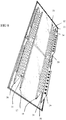
- This support frame 9 comprises, on the one hand, a first part 10 linked to the supporting structure (floor, facade, roof, etc.) and, on the other hand, a second part 11 intended to receive the solar cell, resting on the first part and generally inclined to the horizontal so as to provide optimum orientation with respect to the light radiation.
- the first part 10 of the chassis visible in figure 4 generally comprises a plurality of metal beams 11, 12, 13 arranged between them so as to form a triangulated frame obtained by the assembly of a plurality of parallel trusses connected by beams 14, 15, 16, the beams being intended to receive a plurality of juxtaposed solar modules.
- this frame can be developed from the assembly of a plurality of metal sections of standard section, joined together by any welding-welding process or the like.
- the second part of the frame consists of a set of cross members 17, 18 positioned on the underside of the solar module (back) and oriented parallel to the edges of larger dimension. These sections of polygonal cross section are secured to the underside of the solar module for example by gluing.
- the profiles evenly distributed on the lower face of the element are positioned parallel to the edges small dimensions.
- the profile 17, 18 is obtained by folding or stamping a metal strip, this metal strip having been previously punched so as to form a plurality of holes 29, the material recesses allowing substantially to reduce the mass of the sheet without affecting the mechanical properties.
- This profiled 17, 18 ribbed produces a section of complex section obtained by the juxtaposition edge to edge profile of simple straight section, in particular U, V, convex profile and / or concave.
- the cross section of the profile 17, 18 is generally in the form of inverted 2 V, the junction zones 30, 31 between the V conforming plane portions so as to form contact zones, or with the rear face of the module, either with the supporting structure.
- the profile 17, 18 represented in figures 8 and 9 has a first planar zone 30 extending parallel to one of the sides of the module and intended to form a contact zone with the rear face of the module, for example by gluing. From the longitudinal edge of this flat zone 30 projects a first flange 32 of the V rib, this flange 32 is provided with a plurality of orifices 29 thus making it possible to lighten it without affecting its properties. mechanical (torsion resistance).
- This substantially vertical or oblique wing 32 following the opening of the V, cooperates, at its other longitudinal edge, with another plane zone 31 coplanar with the first, and intended to form a zone of contact with the bearing structure (visible in figure 9 ), this flat area 31 can be hollowed out (holes are visible in figure 9 ) for weight gain problems.
- this wing 33 is also provided with a plurality of orifices 29, obtained by punching the metal foil before folding.
- This second wing 33 is in fact a common wing with the second V-shaped rib.
- This second wing 33 continues with a third flat zone 30 whose role is identical to the first zone (contact zone with the rear face of the module). From the longitudinal edge of this third flat zone 30 extends the last flange 34 of the V-shaped rib, the latter flange 34 being like the previous ones provided with a plurality of orifices 29 for lightening the assembly.
- this latter flange 34 is provided substantially in its central part with a notch 35.
- This notch 35 creates a recess of material or level of the wing, to guarantee access to junction boxes or junction located on the rear side of the module.
- the notch 35 is obtained by cutting the metal sheet before folding.
- the last wing 34 comprises at its longitudinal edge a flat area 36 (visible in figure 10 ) substantially in the same plane as the second plane zone 31 and intended to form a contact zone with the carrier structure.
- the ribbed section is symmetrical and it is sufficient to rotate the latter to achieve, as appears in FIG. figures 8 and 9 , positioning and assembly at a module rear face, of at least 2 ribbed sections from a single model.
- At least one of the flat surfaces 30, 36 intended to come into contact with the rear face of the photovoltaic module is provided with a safety device 40 which retains the module if the latter separates from the ribbed section.
- a safety device 40 which retains the module if the latter separates from the ribbed section.
- This is a tab directly from manufacture during stamping or reported on at least one of said planar surfaces. It will be noted that the length of these tabs is adapted to correspond substantially to one of the specific dimensions of the module (in this case in the figures, it is the length) and ends with a bent part so as to retain by pinching said panel.
- these safety devices 40 will be used when the panels assembled on their supporting structure, are found in an inclined position and because of their own weight may cause their fall.
- the ribbed sections 17, 18 are made of metal, but it is possible to design profiles of identical profile made of plastics material and obtained by a plastic extrusion technique. In this embodiment of plastic, the plastic profiles would be possibly not perforated, in part, the weight gain being achieved by the choice of material.
- the profiles are arranged parallel to one of the edges of the module, so that, when the module is assembled on the superstructure or the support frame, the profile extends vertically and parallel to one of the sides, thus favoring the convection movements and thus the cooling of the module.
- bottom is the face of the support substrate which faces the carrier structure or superstructure.
- each of the integral sections of the modules with a plurality of orifices 19, 20 on the face to be in contact with the chassis.
- Each of these orifices 19, 20 is intended to receive a centering stud 21, 22 or stud projecting from crossbars of the supporting structure (see Figures 5 and 6 ).
- each of these crosspieces comprises at least one orifice 19, 20 (preferably two ) which cooperates with a pin 21, 22 thus allowing the aid of the two cross members to position the module on its supporting structure in all directions of space.
- U-shaped iron portions 23, 24 centered around each of the nipples and whose spacing between the two wings of the U will be chosen to be substantially greater than the thickness of the cross-member and will ensure optimal positioning and will facilitate installation. .
- FIG. 5 A device for locking and unlocking the modules on the supporting structure and is visible in Figures 5, 6 .
- This locking / unlocking device 25 is articulated around an eccentric system which makes it possible to actuate two articulated arms 26, 27, these arms being able to occupy a first so-called locking position (see FIG.
- the eccentric is controlled by a key.
- a quarter-turn movement in a clockwise and then anti-clockwise direction makes it possible to actuate the free end of the arms of the locking / unlocking device in a manner similar to the bolt of a lock.
- each of the studs 21, 22 cooperates with a keyhole-shaped orifice 28 made on the profiles of the supporting structure.
- the diameter restriction of this keyhole shape makes it possible to ensure the mechanical blocking of the module during displacement of the stud within these two orifices, during the relative movement of the module with respect to the bearing structure.
Description
La présente invention est relative à des perfectionnements apportés à des éléments capables de collecter de la lumière.The present invention relates to improvements made to elements capable of collecting light.
Il est connu que des éléments capables de collecter de la lumière du type cellules solaires photovoltaïques comportent un agent absorbant, et deux électrodes électriquement sur n'importe quelle face. L'ensemble est encapsulé entre deux substrats dont l'un étant un substrat de protection à fonction verrière afin de permettre le passage de la lumière et l'autre un substrat support et donc n'est pas nécessairement transparent. Ces électrodes se caractérisent essentiellement par une résistance électrique de surface aussi faible que possible et une bonne adhérence à la couche d'absorbeur ainsi que le cas échéant au substrat. Les électrodes sont la plupart du temps fabriquées en métal ou à partir d'un oxyde métallique, par exemple à base de molybdène, d'argent, d'aluminium, de cuivre, d'oxyde de zinc dopé, ou d'oxyde d'étain.It is known that elements capable of collecting light of the solar photovoltaic cell type comprise an absorbing agent, and two electrodes electrically on any face. The assembly is encapsulated between two substrates, one of which is a protective substrate with glass function to allow the passage of light and the other a support substrate and therefore is not necessarily transparent. These electrodes are characterized essentially by a surface electrical resistance as low as possible and a good adhesion to the absorber layer and, where appropriate, to the substrate. The electrodes are mostly made of metal or from a metal oxide, for example based on molybdenum, silver, aluminum, copper, doped zinc oxide, or aluminum oxide. tin.
Ces éléments capables de la lumière sont assemblés sous la forme d'un vitrage feuilleté qui est emprisonné dans un châssis ou une superstructure métallique devant apporter au vitrage à la fois sa rigidité mécanique et permettre son association avec d'autres vitrages analogues, en vue de l'obtention de surface active de plus grande dimension.These light-capable elements are assembled in the form of a laminated glazing which is trapped in a metal frame or superstructure to bring to the glazing both its mechanical rigidity and its association with other similar glazings, in order to obtaining an active surface of larger size.
Généralement le châssis métallique est réalisé à partir de profilés de section droite en U, les branches du U emprisonnant une portion de surface située en périphérie de chacun des substrats. Ces zones de recouvrement nécessaires à l'assemblage mécanique sont en fait des parties masquées de surface active et constituent des surfaces qui ne peuvent être utilisées pour convertir de la lumière en énergie électrique, diminuant d'autant la surface réelle active. Or, les fabricants certifient leur module en fonction d'une puissance électrique obtenue par unité de surface. Or, on comprend aisément que les fabricants recherchent constamment à ce que l'unité de surface active soit la plus proche possible de la surface réelle du panneau.Generally the metal frame is made from profiles of U-shaped cross-section, the legs of the U trapping a surface portion located at the periphery of each of the substrates. These overlapping areas necessary for mechanical assembly are in fact masked portions of active surface and constitute surfaces that can not be used to convert light into electrical energy, thereby decreasing the actual active area. However, manufacturers certify their module based on an electric power obtained per unit area. It is easy to see that manufacturers are looking for constantly that the active area unit is as close as possible to the actual surface of the panel.
Un deuxième problème lié au mode d'assemblage par châssis métallique a été identifié. Il est relatif à l'échauffement des modules. En effet, lorsque des modules sont assemblés entre eux bord à bord au niveau de leur partie métallique en regard afin de conformer des surfaces de conversion de forte puissance, il a été constaté que la température des modules augmentait compte tenu du réchauffage par le soleil, les parties verticales de la superstructure étant néfastes à l'établissement d'un courant d'air de convection nécessaire au refroidissement. En effet, il est connu que le rendement d'un module solaire ou photovoltaïque est inversement proportionnel à la température desdits modules.A second problem related to the method of assembly by metal frame has been identified. It relates to the heating of the modules. Indeed, when modules are assembled together edge to edge at their metal part facing in order to conform high power conversion surfaces, it was found that the temperature of the modules increased in view of the reheating by the sun, the vertical parts of the superstructure being detrimental to the establishment of a convection air flow necessary for cooling. Indeed, it is known that the efficiency of a solar or photovoltaic module is inversely proportional to the temperature of said modules.
Ce problème d'insuffisance de mouvement de convection ne peut être solutionné par les châssis de l'art antérieur, ils ont atteint leur limite. En effet, il conviendrait que l'assemblage des modules soit assemblé à un support en prenant soin de laisser entre 2 modules un espace permettant le passage d'un courant d'air de convection. Or en procédant ainsi, cela revient à augmenter encore la surface utilisée par rapport à la surface réellement active utile à la conversion énergétique.This problem of insufficient convection movement can not be solved by the chassis of the prior art, they have reached their limit. Indeed, it is appropriate that the assembly of the modules is assembled to a support taking care to leave between 2 modules a space for the passage of a convection air stream. But by doing so, it amounts to further increase the area used compared to the actually active area useful for energy conversion.
La présente invention vise donc à pallier les inconvénients en proposant une technique d'assemblage des modules qui maximise le ratio surface du module par rapport à la surface active du panneau.The present invention therefore aims to overcome the disadvantages by proposing a module assembly technique that maximizes the surface area of the module relative to the active surface of the panel.
A cet effet, la présente invention propose un module solaire selon la revendication 1.For this purpose, the present invention provides a solar module according to
Dans des modes de réalisation préférés de l'invention, on peut éventuellement avoir recours en outre à l'une et/ou à l'autre des dispositions suivantes :
- l'élément est sensiblement de forme polygonale, notamment rectangulaire,
- l'élément comporte sur sa face inférieure aux moins 2 profilés orientés parallèlement aux côtés situés verticalement, lorsque l'élément est assemblé à une superstructure.
- il comporte un dispositif de verrouillage et de déverrouillage desdits éléments à une structure porteuse,
- le dispositif de verrouillage comporte un trou de serrure,
- les profilés sont assemblés par collage à une portion de surface du substrat support.
- l'une des zones de contact comporte un dispositif de sécurité.
- l'une des zones de contact comporte un talon avec une bride et un organe de serrage solidaire de la superstructure
- the element is substantially of polygonal shape, in particular rectangular,
- the element has on its underside at least 2 sections oriented parallel to the vertically located sides, when the element is assembled to a superstructure.
- it comprises a device for locking and unlocking said elements to a supporting structure,
- the locking device comprises a keyhole,
- the profiles are assembled by gluing to a surface portion of the support substrate.
- one of the contact zones comprises a safety device.
- one of the contact zones comprises a heel with a flange and a clamping member integral with the superstructure
Selon un autre aspect de l'invention, elle vise également une table adaptée pour être solidarisée à une structure porteuse comprenant une pluralité d'éléments juxtaposés tels que précédemment décrits.According to another aspect of the invention, it also relates to a table adapted to be secured to a carrier structure comprising a plurality of elements juxtaposed as previously described.
Selon une caractéristique préférentielle, la table possède un gabarit compatible avec un moyen de transport de type « Inloader ».According to a preferred feature, the table has a template compatible with an "Inloader" type of transport means.
D'autres caractéristiques, détails, avantages de la présente invention apparaîtront mieux à la lecture de la description qui va suivre, faite à titre illustratif et nullement limitatif, en référence à des figures annexées sur lesquelles :
- Les
figures 1a et1b est une vue en perspective d'un élément capable de collecter de la lumière, - Les
figures 2 et 3 sont des vues schématiques d'un élément capable de collecter de la lumière - la
figure 4 est une vue en perspective d'une structure porteuse supportant des tables, chacune de ces tables comportant une juxtaposition d'éléments selon les figures la et 1b, - les
figures 5 et 6 sont des vues à grande échelle et en perspective du système de solidarisation permettant l'accrochage mécanique entre un module et la charpente. - La
figure 7 illustre un second mode de verrouillage, en forme de trou de serrure. - La
figure 8 est une vue de dessous et en perspective d'une structure porteuse supportant un élément capable de collecter de la lumière, - La
figure 9 est une vue en perspective d'une structure porteuse représentée sans la table - La
figure 10 est une vue de détail et en perspective de la structure porteuse.
- The
figures 1a and1b is a perspective view of an element capable of collecting light, - The
Figures 2 and 3 are schematic views of an element capable of collecting light - the
figure 4 is a perspective view of a supporting structure supporting tables, each of these tables comprising a juxtaposition of elements according to Figures la and 1b, - the
Figures 5 and 6 are large-scale and perspective views of the fastening system allowing the mechanical attachment between a module and the frame. - The
figure 7 illustrates a second locking mode, in the form of a keyhole. - The
figure 8 is a view from below and in perspective of a supporting structure supporting an element capable of collecting light, - The
figure 9 is a perspective view of a bearing structure represented without the table - The
figure 10 is a detail and perspective view of the supporting structure.
Sur la figure la, on a représenté un élément capable de collecter de la lumière (une cellule solaire ou photovoltaïque). Schématiquement, deux substrats 1 et 1', dont l'un au moins est nécessairement transparent pour laisser passer la lumière, emprisonnent un empilement de couches 7, comportant entre des couches électroconductrices 2, 6 formant électrodes, une couche fonctionnelle 3 à base d'agent absorbant permettant la conversion énergétique de la lumière en énergie électrique. Ces empilements sont visibles en
Le substrat 1 formant couvercle est transparent et peut par exemple être entièrement en verre. Il peut également être en un polymère thermoplastique tel qu'un polyuréthane ou un polycarbonate ou un polyméthacrylate de méthyle.The
L'essentiel de la masse (c'est-à-dire pour au moins 98 % en masse), voire la totalité du substrat à fonction verrière est constituée de matériau(x) présentant la meilleure transparence possible et ayant de préférence une absorption linéique inférieure à 0,01 mm-1 dans la partie du spectre utile à l'application (module solaire), généralement le spectre allant de 380 à 1200 nm.Most of the mass (that is to say at least 98% by weight), or even the entire glass-function substrate consists of material (x) having the best possible transparency and preferably having a linear absorption. less than 0.01 mm -1 in the part of the spectrum useful for the application (solar module), generally the spectrum ranging from 380 to 1200 nm.
Le substrat 1 formant couvercle selon l'invention peut avoir une épaisseur totale allant de 0,5 à 10 mm lorsqu'on l'utilise comme plaque protectrice d'une cellule photovoltaïque de diverses technologies (CIS, silicium amorphe, silicium micro cristallin, silicium cristallin). Dans ce cas, il peut être avantageux de faire subir à cette plaque un traitement thermique (du type trempe par exemple) lorsqu'il est en verre.The
La technologie CIS rassemble des composés ternaires chalcopyrites qui jouent le rôle d'agents absorbeurs, ces derniers contiennent généralement du cuivre, de l'indium et du sélénium. Il s'agit là de ce que l'on appelle des couches d'agent absorbant CISe2. On peut aussi ajouter à la couche d'agent absorbant du gallium (ex : Cu(In,Ga)Se2 ou CuGaSe2), de l'aluminium (ex : Cu(In,Al)Se2), ou du soufre (ex : CuIn(Se,S). On les désigne en général et ci-après par le terme de couches d'agent absorbant à chalcopyrite.The CIS technology combines ternary chalcopyrite compounds that act as absorbers, the latter usually containing copper, indium and selenium. These are so-called CISe 2 absorbent layers. The gallium absorbing agent layer (eg Cu (In, Ga) Se 2 or CuGaSe 2 ), aluminum (eg Cu (In, Al) Se 2 ), or sulfur ( Examples: CuIn (Se, S) and are generally referred to herein as "chalcopyrite adsorbent layers".
Une autre famille d'agent absorbant, en couche mince, est soit à base de silicium, ce dernier pouvant être amorphe ou microcristallin, soit à base de tellure de cadmium (CdTe). Il existe également une autre famille d'agent absorbant à base de silicium polycristallin, déposé en couche épaisse, avec une épaisseur comprise entre 50 µm à 250 µm, au contraire de la filière silicium amorphe ou microcristallin, qui est déposé en couche mince.Another family of absorbent agent, in a thin layer, is either based on silicon, the latter may be amorphous or microcrystalline, or based on cadmium telluride (CdTe). There is also another family of polycrystalline silicon-based absorbent agent, deposited in a thick layer, with a thickness of between 50 microns and 250 microns, unlike the amorphous or microcrystalline silicon die, which is deposited in a thin layer.
Le substrat 1' formant plaque support diffère du substrat 1 par le fait qu'il n'est pas nécessairement transparent, et donc pas nécessairement à fonction verrière.The substrate 1 'forming a support plate differs from the
En référence à la
La couche d'agent absorbant à chalcopyrite 3 est revêtue d'une fine couche 4 dite tampon en sulfure de cadmium (CdS), en sulfure de zinc (ZnS), ou en sulfure d'indium (IS) permettant de créer avec la couche à chalcopyrite une jonction pn. En effet, l'agent à chalcopyrite est généralement dopé p, la couche tampon, notamment en CdS, étant dopée n, cela permet de créer la jonction pn nécessaire à l'établissement d'un courant électrique.The layer of
Cette fine couche tampon 4 par exemple en CdS est elle-même recouverte d'une couche d'accrochage 5 généralement formée d'oxyde de zinc non dopée (ZnO).This
Afin de former la seconde électrode 6, la couche de ZnO 5 est recouverte d'une couche en TCO pour « Transparent Conductive Oxide ». Elle peut être choisie parmi les matériaux suivants : oxyde d'étain dopé, notamment en bore, ou en aluminium. Dans le cas de l'oxyde de zinc dopé, notamment à l'aluminium, les précurseurs utilisables, en cas de dépôt par CVD, peuvent être des organo-métalliques ou halogénures de zinc et d'aluminium. L'électrode en TCO, par exemple en ZnO peut être aussi déposée par pulvérisation à partir de cible métallique ou céramique.In order to form the
Par ailleurs, cette couche conductrice doit être aussi transparente que possible, et présenter une transmission élevée de la lumière dans l'ensemble des longueurs d'onde correspondant au spectre d'absorption du matériau constituant la couche fonctionnelle, afin de ne pas réduire inutilement le rendement du module solaire.Moreover, this conductive layer must be as transparent as possible, and have a high transmission of light in all wavelengths corresponding to the absorption spectrum of the material constituting the functional layer, so as not to reduce unnecessarily the solar module efficiency.
L'une ou l'autre des couches conductrices 2, 6 présente résistance par carré d'au plus 30 ohms/carré, notamment d'au plus 20 ohms/carré, de préférence d'au plus 10 ou 15 ohms/carré. Elle est généralement comprise entre 5 et 12 ohms/carré.One or the other of the
L'empilement 7 de couches minces est emprisonné entre les deux substrats formant couvercle 1 et support 1' par l'intermédiaire d'un intercalaire de feuilletage 8 par exemple en PU, PVB ou EVA. Le substrat 1 se distingue du substrat 1' par le fait qu'il est à fonction verrière, comme un verre silico-sodo-calcique de manière à conformer une cellule solaire ou photovoltaïque puis encapsulé périphériquement à l'aide d'un joint ou d'une résine d'étanchéité. Un exemple de composition de cette résine et de ses modalités de mise en oeuvre est décrit dans la demande
Si on utilise un agent absorbant de la filière silicium en couche mince, à savoir du silicium amorphe, ou du silicium micro cristallin, ou un agent absorbant à base de tellure de cadmium (CdTe) en couche mince, la construction de l'élément capable de collecter de la lumière est réalisée en sens inverse de celui utilisé pour la filière à chalcopyrite. On parle alors de construction dite à « superstrate » par opposition à la construction dite à « strate ». On pourra se reporter à la
La différence essentielle réside dans le fait que l'empilement de couches minces est construit à partir du substrat 1 formant couvercle. La face B (la face principale interne) du substrat 1 est revêtue d'une première couche conductrice 6 devant servir d'électrode. Sur cette électrode est déposée la couche fonctionnelle à base d'agent absorbant en silicium amorphe ou microcristallin ou en tellure de cadmium.The essential difference lies in the fact that the stack of thin layers is constructed from the
Afin de former la première électrode 6, la couche est à base d'une couche en TCO pour « Transparent Conductive Oxide » .Elle peut être choisie parmi les matériaux suivants : oxyde d'étain dopé, notamment en bore, ou en aluminium. Dans le cas de l'oxyde de zinc dopé, notamment à l'aluminium, les précurseurs utilisables, en cas de dépôt par CVD, peuvent être des organo-métalliques ou halogénures de zinc et d'aluminium. L'électrode en TCO, par exemple en ZnO peut être aussi déposée par pulvérisation à partir de cible métallique ou céramique.In order to form the
Cette couche conductrice doit être aussi transparente que possible, et présenter une transmission élevée de la lumière dans l'ensemble des longueurs d'onde correspondant au spectre d'absorption du matériau constituant la couche fonctionnelle, afin de ne pas réduire inutilement le rendement du module solaire.This conductive layer must be as transparent as possible, and have a high transmission of light in all wavelengths corresponding to the absorption spectrum of the material constituting the functional layer, so as not to reduce the efficiency of the module unnecessarily. solar.
Cette couche 6 de TCO, à base par exemple de SnO2 : F ou de ZnO :A1 est éventuellement recouverte d'une couche 5 additionnelle relativement mince (par exemple 100 nm) en ZnO non dopée. Cette couche mince de ZnO est ensuite recouverte de la couche fonctionnelle 3 à base de silicium ou de tellure de cadmium en couche mince. Le reste de l'empilement 7 est constitué d'une deuxième couche conductrice 2 servant d'électrode en matériau métallique ou d'oxyde métallique. Classiquement cette couche conductrice est à base d'ITO (oxyde d'indium et d'étain) ou en métal (cuivre, aluminium)
L'une ou l'autre des couches conductrices 2, 6 présente résistance par carré d'au plus 30 ohms/carré, notamment d'au plus 20 ohms/carré, de préférence d'au plus 10 ou 15 ohms/carré. Elle est généralement comprise entre 5 et 12 ohms/carré.This
One or the other of the
L'empilement de couches minces est emprisonné entre les deux substrats 1 et 1' par l'intermédiaire d'un intercalaire de feuilletage 8 par exemple en PU, PVB ou EVA. Le substrat 1' se distingue du substrat 1 par le fait qu'il n'est pas nécessairement en verre et n'est pas forcément transparent. Il joue un rôle de support et est encapsulé avec l'autre substrat 1 périphériquement à l'aide d'un joint ou d'une résine d'étanchéité. Un exemple de composition de cette résine et de ses modalités de mise en oeuvre est décrit dans la demande
Une troisième configuration consiste en à la réalisation d'élément (modules solaires) dont l'agent absorbant est à base silicium cristallin. Les wafers de silicium sont alors assemblés par l'intermédiaire d'un intercalaire de feuilletage en EVA, PU, ou PVB entre les deux substrats 1,1' formant respectivement le couvercle et le support de l'élément. Les couches électroconductrices 2, 6 formant les électrodes, en couches ou en grilles, sont déposées sur chacun des substrats et sont obtenues par une technique de sérigraphie de composés métalliques.A third configuration consists in the realization of element (solar modules) whose absorbent agent is based on crystalline silicon. The silicon wafers are then assembled via an EVA, PU or PVB lamination interlayer between the two
Un module solaire tel que précédemment décrit, doit, pour pouvoir fonctionner et délivrer une tension électrique à un réseau de distribution électrique, être pourvu de moyens de support et de solidarisation assurant son orientation par rapport au rayonnement lumineux.A solar module as previously described, must, in order to operate and deliver an electrical voltage to an electrical distribution network, be provided with support and securing means ensuring its orientation with respect to the light radiation.
Pour ce faire et on pourra se reporter à la
La première partie 10 du châssis visible en
Classiquement ce châssis peut être élaboré à partir de l'assemblage d'une pluralité de profilés métalliques de section standard, solidarisés entre eux par tout procédé de mécano-soudage ou similaire.Conventionally this frame can be developed from the assembly of a plurality of metal sections of standard section, joined together by any welding-welding process or the like.
Selon un mode préféré de réalisation (se reporter à la figure la), la seconde partie du châssis est constituée par un ensemble de traverses 17, 18 positionnées sur la face inférieure du module solaire (au dos) et orientées parallèlement aux bords de plus grande dimension. Ces profilés de section droite polygonale sont solidarisés à la face inférieure du module solaire par exemple par collage.According to a preferred embodiment (see Figure la), the second part of the frame consists of a set of
Selon un autre mode de réalisation (se reporter à la
Selon l'invention (se reporter aux
La section droite du profilé 17, 18 se présente globalement sous la forme de 2 V inversés, les zones de jonction 30, 31 entre les V conformant des parties planes de manière à conformer des zones de contact, soit avec la face arrière du module, soit avec la structure porteuse.The cross section of the
Ainsi le profilé 17, 18 représenté en
Du bord longitudinal de cette deuxième zone plane 31 s'étend en saillie la deuxième aile 33 conformant la nervure en V, de manière similaire à la précédente, cette aile 33 est également pourvue d'une pluralité d'orifices 29, obtenus par poinçonnage de la feuille métallique avant son pliage. Cette deuxième aile 33 constitue en fait une aile commune avec la deuxième nervure en V. Cette deuxième aile 33 se poursuit par une troisième zone plane 30 dont le rôle est identique à la première zone (zone de contact avec la face arrière du module). Depuis le bord longitudinal de cette troisième zone plane 30 s'étend la dernière aile 34 de la nervure en V, cette dernière aile 34 étant comme les précédentes munies d'une pluralité d'orifices 29 pour l'allégement de l'ensemble.From the longitudinal edge of this second
Comme on peut le voir sur les
La dernière aile 34 comporte au niveau de son bord longitudinal une zone plane 36 (visible en
Elle se distingue cependant par le fait qu'elle comporte un talon 37 permettant le serrage avec une bride 38 et un organe de serrage 39 solidaire de la superstructure ou de la structure porteuse. La bride, lorsqu'elle est desserrée de la structure porteuse, peut aisément se déplacer le long du talon, donnant ainsi quelques degrés de liberté pour l'assemblage des modules à la structure porteuse.However, it is distinguished by the fact that it comprises a
L'assemblage d'un module à la structure porteuse est visible en
Selon une caractéristique préférée de l'invention, le profilé nervuré est symétrique et il suffit de procéder à une rotation de ce dernier pour réaliser, comme cela apparaît en
Selon une autre caractéristique préférée de l'invention, l'une au moins des surfaces planes 30, 36 destinées à venir au contact de la face arrière du module photovoltaïque est pourvue d'un dispositif de sécurité 40 qui retient le module si ce dernier se désolidarise du profilé nervuré. Il s'agit de patte venue directement de fabrication lors de l'emboutissage ou rapportée sur l'une au moins desdites surfaces planes. On pourra remarquer que la longueur de ces pattes est adaptée pour correspondre sensiblement à l'une des dimensions spécifiques du module (en l'espèce sur les figures, il s'agit de la longueur) et se termine par une partie recourbée de manière retenir par pincement ledit panneau.According to another preferred feature of the invention, at least one of the
En général, ces dispositifs de sécurité 40 seront utilisés lorsque les panneaux assemblés sur leur structure porteuse, se retrouvent dans une position inclinée et du fait de leur poids propre peut entraîner leur chute.In general, these
Dans les exemples représentés sur les
Quel que soit le mode de réalisation, les profilés sont disposés parallèlement à l'un des bords du module, de manière à ce que, lorsque le module est assemblé sur la superstructure ou le châssis support, le profilé s'étend verticalement et parallèlement à l'un des côtés, favorisant ainsi les mouvements de convection et donc le refroidissement du module.Whatever the embodiment, the profiles are arranged parallel to one of the edges of the module, so that, when the module is assembled on the superstructure or the support frame, the profile extends vertically and parallel to one of the sides, thus favoring the convection movements and thus the cooling of the module.
Au sens de l'invention « inférieure » est la face du substrat support qui fait face à la structure porteuse ou superstructure.In the sense of the invention "bottom" is the face of the support substrate which faces the carrier structure or superstructure.
Afin de permettre le maintien en position et dans une configuration spatiale figée des modules sur le châssis, on prévoit de pourvoir chacun des profilés solidaires des modules d'une pluralité d'orifices 19, 20, sur la face devant être en contact du châssis. Chacun de ces orifices 19, 20 est destiné à recevoir un plot de centrage 21, 22 ou téton faisant saillie sur des traverses de la structure porteuse (se reporter en
Un dispositif de verrouillage et de déverrouillage des modules sur la structure porteuse et est visible en
Comme cela apparaît en
Selon un autre mode de réalisation du système de verrouillage (cf
Afin de faciliter la logistique, la manipulation, le stockage, on prévoit d'agencer les modules en table (se reporter à la
- une table correspond en fait sensiblement à la dimension interne des remorques de camion spécialement conçues pour le transport de verre. En variante, la table peut être une dimension correspondant à un sous-multiple de la dimension interne des remorques. Une description de ces remorques de camions ou de ces camions couramment dénommés sous le vocable anglais de « Inloader » est donnée par exemple dans les demandes
FR2581603 FR2867118 - Chacune des tables délivre approximativement une unité énergétique (UE) donnée, qui sera facile de comptabiliser et multiplier pour obtenir la puissance désirée
- Il est possible d'utiliser les rotations des « inloader » d'une manière optimale, ces derniers pouvant par exemple apporter à l'unité de fabrication des modules solaires des substrats à fonction verrière de dimensions en PLF (Plateau Largeur Fabrication) ou DLF (Découpé Largeur Fabrication) et repartir, lorsque ces modules sont fabriqués et agencés en table, avec les tables prêtes à être livrées au client final. (Il y a ainsi une gestion optimale des flux de matière et des moyens de transport).
- a table corresponds in fact substantially to the internal dimension of truck trailers specially designed for the transport of glass. Alternatively, the table may be a dimension corresponding to a submultiple of the dimension internal trailers. A description of these trailers of trucks or of these trucks commonly referred to as "Inloader" is given for example in the applications
FR2581603 FR2867118 - Each of the tables delivers approximately one given energy unit (UE), which will be easy to count and multiply to obtain the desired power
- It is possible to use the rotations of the "inloader" in an optimal way, the latter being able for example to bring to the manufacturing unit of the solar modules substrates with glass function of dimensions in PLF (Platform Wide Width Manufacture) or DLF ( Cut Width Manufacturing) and restart, when these modules are manufactured and arranged in a table, with tables ready to be delivered to the end customer. (There is thus optimal management of material flows and means of transport).
Claims (12)
- Solar module capable of collecting light, comprising a first substrate (1) having a glass function and forming a cover and a second substrate (1') forming a support, the substrates (1, 1') sandwiching between two electrode-forming conductive layers (2, 6) at least one functional layer (7) based on an absorber material for converting light energy into electrical energy, the module further comprising at least two ribbed profiles (17, 18) fastened to the lower face of the second substrate (1'), wherein the profiles (17, 18) are oriented parallel to one of the sides of the module and are uniformly distributed on said lower face, wherein each profile (17, 18) has a cross section in the form of two inverted Vs with convex and/or concave form obtained by the edge-to-edge juxtaposition of simple straight sections, wherein each profile (17, 18) is obtained by bending or stamping a metal sheet, and wherein each profile (17, 18) comprises:a first flat region (30) extending parallel to one of the sides of the module configured to form a contact region for contact with the rear face of the second substrate (1'),a first arm (32) projecting from a longitudinal edge of the first flat region (30), the first arm (32) being provided with a plurality of orifices (29) without thereby affecting the mechanical properties thereof,a second flat region (31) parallel to the first flat region (30) projecting from the first arm at its other longitudinal edge configured to form a contact region for contact with a carrier structure,a second arm (33) projecting from the longitudinal edge of the second flat region (31), the second arm (33) being provided with a plurality of orifices (29) without thereby affecting the mechanical properties thereof,a third flat region (30) parallel to the first flat region (30) projecting from the second arm (33) at its other longitudinal edge configured to form a contact region for contact with the rear face of the second substrate (1'),a third arm (34) projecting from the longitudinal edge of the third flat region (30), the third arm (34) being provided with a plurality of orifices (29) without thereby affecting the mechanical properties thereof and in its central part with a notch (35) creating a removal of material so as to ensure access to the connection and junction boxes located on the rear face of the module,a fourth flat region (36) parallel to the second flat region (31) projecting from the third arm (34) at its other longitudinal edge configured to form a contact region for contact with the carrier structure,wherein the first arm (32) and the second arm (33) form a first V and the second arm (33) and the third arm (34) form a second V, with the second V being inverted with respect to the first V.
- Solar module according to claim 1, characterized in that it is of substantially polygonal, in particular rectangular, shape.
- Solar module according to claim 1 or 2, characterized in that it comprises, fastened to its lower face, at least two profiles (17, 18) oriented so as to be parallel to the vertically located sides of the element when the element is assembled with the carrier structure.
- Solar module according to any one of claims 1 through 3, characterized in that at least one of the profiles (17, 18) comprises a safety device (40) in the form of a leg terminated by a curved part, to retain the element if the latter is disconnected from the profile.
- Solar module according to any one of claims 1 through 4, characterized in that each profile (17, 18) comprises, at one of the contact regions (36) with the carrier structure, a lug (37) suitable for being clamped relative to the carrier structure, with a clamp (38) and a tightening member (39) connected to the carrier structure.
- Solar module according to claim 5, characterized in that the lug (37) is suitable for being clamped relative to the carrier structure with the clamp (38) and the tightening member (39) from the upper side of the module.
- Solar module according to any one of the preceding claims, characterized in that it comprises a device (25, 26, 27) for locking said module to the carrier structure.
- Solar module according to claim 7, characterized in that the locking device has a keyhole (28).
- Solar module according to any one of the preceding claims, characterized in that each profile (17, 18) includes at least one orifice for centering said module on the carrier structure.
- Solar module according to one of the preceding claims, characterized in that each profile (17, 18) is assembled by adhesive bonding to a surface portion of the second substrate (1').
- Table, suitable for being fastened to a carrier structure, comprising a plurality of juxtaposed modules elements according to any one of the preceding claims.
- Table according to claim 11, characterized in that it has a size compatible with an "Inloader"-type means of transport.
Applications Claiming Priority (3)
| Application Number | Priority Date | Filing Date | Title |
|---|---|---|---|
| FR0758350A FR2922365B1 (en) | 2007-10-16 | 2007-10-16 | IMPROVEMENTS TO ELEMENTS CAPABLE OF COLLECTING LIGHT. |
| FR0852216A FR2922366B1 (en) | 2007-10-16 | 2008-04-03 | IMPROVEMENTS ON ELEMENTS CAPABLE OF COLLECTING LIGHT |
| PCT/EP2008/063744 WO2009050144A1 (en) | 2007-10-16 | 2008-10-13 | Improvements to light-collecting elements |
Publications (2)
| Publication Number | Publication Date |
|---|---|
| EP2212919A1 EP2212919A1 (en) | 2010-08-04 |
| EP2212919B1 true EP2212919B1 (en) | 2019-08-21 |
Family
ID=39473142
Family Applications (1)
| Application Number | Title | Priority Date | Filing Date |
|---|---|---|---|
| EP08805260.0A Active EP2212919B1 (en) | 2007-10-16 | 2008-10-13 | Improvements to light-collecting elements |
Country Status (9)
| Country | Link |
|---|---|
| US (1) | US9097442B2 (en) |
| EP (1) | EP2212919B1 (en) |
| JP (1) | JP5368461B2 (en) |
| KR (1) | KR101509841B1 (en) |
| CN (1) | CN101897035B (en) |
| ES (1) | ES2757572T3 (en) |
| FR (2) | FR2922365B1 (en) |
| MX (1) | MX2010004027A (en) |
| WO (1) | WO2009050144A1 (en) |
Families Citing this family (13)
| Publication number | Priority date | Publication date | Assignee | Title |
|---|---|---|---|---|
| US8586398B2 (en) * | 2008-01-18 | 2013-11-19 | Miasole | Sodium-incorporation in solar cell substrates and contacts |
| US8546172B2 (en) | 2008-01-18 | 2013-10-01 | Miasole | Laser polishing of a back contact of a solar cell |
| JP5263795B2 (en) * | 2010-03-25 | 2013-08-14 | シャープ株式会社 | Solar cell module mounting structure |
| US8584338B2 (en) * | 2010-05-24 | 2013-11-19 | Chevron U.S.A. Inc. | Solar module array pre-assembly method |
| CN102005977B (en) * | 2010-11-30 | 2012-06-13 | 阿特斯(中国)投资有限公司 | Roof photovoltaic power generation system |
| DE112012001993T8 (en) * | 2011-05-06 | 2014-06-26 | Mitsubishi Electric Corporation | Solar battery system and solar battery module |
| WO2013028969A1 (en) * | 2011-08-24 | 2013-02-28 | Corning Incorporated | Photovoltaic assembly comprising an array of load compensating pv modules |
| IN2014DN10302A (en) * | 2012-05-03 | 2015-08-07 | Changzhou Trina Solar Energy | |
| JP2014034764A (en) * | 2012-08-07 | 2014-02-24 | Sharp Corp | Solar cell module trestle, solar cell module installation structure, solar cell module installation method, and photovoltaic power generation system |
| EP3182580A1 (en) * | 2015-12-15 | 2017-06-21 | ML SYSTEM Spólka Akcyjna | A photovoltaic module for ventilated facade and a set of inner components of the facade fixing it to face walls of a building and joining the module with the inner structure of the facade |
| US11139776B2 (en) * | 2016-07-01 | 2021-10-05 | Sunpower Corporation | Photovoltaic panel having a distributed support frame |
| US11411530B2 (en) * | 2016-10-11 | 2022-08-09 | Greenti Sagl | Photovoltaic element and mounted surface comprising such photovoltaic elements |
| ES2727259A1 (en) * | 2018-04-12 | 2019-10-15 | Gonzalez Soria Juan Carlos | System for fixing solar modules to support structures (Machine-translation by Google Translate, not legally binding) |
Citations (3)
| Publication number | Priority date | Publication date | Assignee | Title |
|---|---|---|---|---|
| US20030154667A1 (en) * | 2002-02-20 | 2003-08-21 | Dinwoodie Thomas L. | Shingle system |
| JP2004324233A (en) * | 2003-04-24 | 2004-11-18 | Kyocera Corp | Method of mounting solar battery module |
| DE102004055187A1 (en) * | 2004-11-16 | 2006-05-24 | Blitzstrom Gmbh | Profile bar for photovoltaic module, has groove which divides carrier part into two carrier strips which are interrelated at groove base, where even outer surface of carrier part adheres with module |
Family Cites Families (27)
| Publication number | Priority date | Publication date | Assignee | Title |
|---|---|---|---|---|
| JPS6186958U (en) * | 1984-11-12 | 1986-06-07 | ||
| DE3516914A1 (en) * | 1985-05-10 | 1986-11-13 | VEGLA Vereinigte Glaswerke GmbH, 5100 Aachen | Transport device for packages of glass panes with large dimensions |
| US5143556A (en) | 1989-03-13 | 1992-09-01 | Matlin Ronald W | Support for photovoltaic arrays |
| DE4014200A1 (en) * | 1989-05-18 | 1990-11-22 | Telefunken Systemtechnik | Frameless solar generator - with solar cell laminate resting on profiles with silicone adhesive pads |
| US5180442A (en) * | 1992-04-06 | 1993-01-19 | Eric Elias | Integration system for solar modules |
| JPH08181345A (en) * | 1994-12-21 | 1996-07-12 | Ykk Kk | Mounting structure of solar cell module |
| DE19529351A1 (en) * | 1995-08-09 | 1997-02-13 | Gido Genschorek | Device for fastening plate-shaped components, in particular solar modules and solar panels |
| JPH1054118A (en) * | 1996-08-08 | 1998-02-24 | Canon Inc | Solar cell module |
| US6201179B1 (en) * | 1997-10-03 | 2001-03-13 | Nick Dalacu | Array of photovoltaic modules for an integrated solar power collector system |
| US6111189A (en) * | 1998-07-28 | 2000-08-29 | Bp Solarex | Photovoltaic module framing system with integral electrical raceways |
| JP2000079961A (en) * | 1998-09-01 | 2000-03-21 | Misawa Homes Co Ltd | Method for transporting roof panel with solar battery and device for transporting the same |
| GB9820133D0 (en) * | 1998-09-16 | 1998-11-11 | Reardon Martin | Guagemaster roof system |
| US6722357B2 (en) * | 2001-08-15 | 2004-04-20 | Powerlight Corporation | Fixed angle solar collector arrangement |
| US6672018B2 (en) * | 2001-10-12 | 2004-01-06 | Jefferson Shingleton | Solar module mounting method and clip |
| AU2003256377A1 (en) * | 2002-07-05 | 2004-01-23 | Golden Solar Energy, Inc. | Apparatus, system, and method of diagnosing individual photovoltaic cells |
| US8344239B2 (en) * | 2004-02-13 | 2013-01-01 | Pvt Solar, Inc. | Mechanism for mounting solar modules |
| DE102004009935A1 (en) * | 2004-02-26 | 2005-09-15 | Müller, Franz | Method and system for fixing panel elements |
| US7406800B2 (en) * | 2004-05-18 | 2008-08-05 | Andalay Solar, Inc. | Mounting system for a solar panel |
| EP1601022A1 (en) * | 2004-05-28 | 2005-11-30 | Hilber Technic Cooperation GmbH | Solar installation |
| CN2708507Y (en) * | 2004-06-02 | 2005-07-06 | 张云峰 | Solar cell mounting structure |
| EP1813738B1 (en) * | 2004-10-22 | 2018-11-28 | Kyocera Corporation | Solar battery module device and method of installing the same |
| JP2006278738A (en) * | 2005-03-29 | 2006-10-12 | Kyocera Corp | Photovoltaic power generating apparatus |
| JPWO2006121013A1 (en) * | 2005-05-11 | 2008-12-18 | 株式会社カネカ | Solar cell module and solar cell installation surface |
| WO2006132265A1 (en) * | 2005-06-07 | 2006-12-14 | Sharp Kabushiki Kaisha | Condensing photovoltaic power generation unit and condensing photovoltaic power generation system, and condensing lens, condensing lens structure, and production method of condensing lens structure |
| DE102005057468A1 (en) * | 2005-11-30 | 2007-05-31 | Solarwatt Solar-Systeme Ag | Plate-shaped frameless photovoltaic solar module has solar cells embedded between cover and rear materials and a rear strengthening structure |
| WO2008124158A1 (en) * | 2007-04-06 | 2008-10-16 | West John R | Method and apparatus for forming and mounting a photovoltaic array |
| WO2009015106A2 (en) * | 2007-07-20 | 2009-01-29 | Robert Stancel | Rapid mounting system for solar modules |
-
2007
- 2007-10-16 FR FR0758350A patent/FR2922365B1/en active Active
-
2008
- 2008-04-03 FR FR0852216A patent/FR2922366B1/en active Active
- 2008-10-13 MX MX2010004027A patent/MX2010004027A/en active IP Right Grant
- 2008-10-13 US US12/738,218 patent/US9097442B2/en active Active
- 2008-10-13 JP JP2010529351A patent/JP5368461B2/en active Active
- 2008-10-13 ES ES08805260T patent/ES2757572T3/en active Active
- 2008-10-13 EP EP08805260.0A patent/EP2212919B1/en active Active
- 2008-10-13 KR KR1020107010595A patent/KR101509841B1/en active IP Right Grant
- 2008-10-13 WO PCT/EP2008/063744 patent/WO2009050144A1/en active Application Filing
- 2008-10-13 CN CN2008801208777A patent/CN101897035B/en active Active
Patent Citations (3)
| Publication number | Priority date | Publication date | Assignee | Title |
|---|---|---|---|---|
| US20030154667A1 (en) * | 2002-02-20 | 2003-08-21 | Dinwoodie Thomas L. | Shingle system |
| JP2004324233A (en) * | 2003-04-24 | 2004-11-18 | Kyocera Corp | Method of mounting solar battery module |
| DE102004055187A1 (en) * | 2004-11-16 | 2006-05-24 | Blitzstrom Gmbh | Profile bar for photovoltaic module, has groove which divides carrier part into two carrier strips which are interrelated at groove base, where even outer surface of carrier part adheres with module |
Also Published As
| Publication number | Publication date |
|---|---|
| CN101897035B (en) | 2013-05-08 |
| US9097442B2 (en) | 2015-08-04 |
| KR20100094462A (en) | 2010-08-26 |
| ES2757572T3 (en) | 2020-04-29 |
| FR2922366B1 (en) | 2010-06-04 |
| FR2922365A1 (en) | 2009-04-17 |
| EP2212919A1 (en) | 2010-08-04 |
| FR2922366A1 (en) | 2009-04-17 |
| MX2010004027A (en) | 2010-06-01 |
| JP5368461B2 (en) | 2013-12-18 |
| JP2011501424A (en) | 2011-01-06 |
| KR101509841B1 (en) | 2015-04-06 |
| FR2922365B1 (en) | 2009-12-18 |
| US20100258158A1 (en) | 2010-10-14 |
| CN101897035A (en) | 2010-11-24 |
| WO2009050144A1 (en) | 2009-04-23 |
Similar Documents
| Publication | Publication Date | Title |
|---|---|---|
| EP2212919B1 (en) | Improvements to light-collecting elements | |
| EP2430378B1 (en) | Arrangement comprising an attachment device and method for mounting this arrangement | |
| EP2227829B2 (en) | Improvements to elements capable of collecting light | |
| FR2949548A1 (en) | SYSTEM FOR MOUNTING PHOTOVOLTAIC MODULES | |
| FR2613130A1 (en) | MODULE OF PHOTOELECTRIC SOLAR CELLS | |
| EP2212924B1 (en) | Improvements to a connection housing for light-capturing elements | |
| WO2011004329A1 (en) | Method for manufacturing photovoltaic cells with multiple junctions and multiple electrodes | |
| EP3493277B1 (en) | Method for interconnecting photovoltaic cells with an electrode having metal nanowires | |
| EP2212925B1 (en) | Improvements made to seals for light-capturing elements | |
| EP2208235B1 (en) | Glass substrate for solar cells | |
| EP4002491A1 (en) | Improved light and flexible photovoltaic module | |
| FR3074963A1 (en) | PHOTOVOLTAIC MODULE COMPRISING PHOTOVOLTAIC CELLS INTERCONNECTED BY INTERCONNECTION ELEMENTS | |
| EP3809473A1 (en) | Method for interconnection of photovoltaic cells with metal wires in contact with pads of solder paste | |
| KR20180055542A (en) | Solar cell pannel and method for manufacturing the same |
Legal Events
| Date | Code | Title | Description |
|---|---|---|---|
| PUAI | Public reference made under article 153(3) epc to a published international application that has entered the european phase |
Free format text: ORIGINAL CODE: 0009012 |
|
| 17P | Request for examination filed |
Effective date: 20100517 |
|
| AK | Designated contracting states |
Kind code of ref document: A1 Designated state(s): AT BE BG CH CY CZ DE DK EE ES FI FR GB GR HR HU IE IS IT LI LT LU LV MC MT NL NO PL PT RO SE SI SK TR |
|
| AX | Request for extension of the european patent |
Extension state: AL BA MK RS |
|
| DAX | Request for extension of the european patent (deleted) | ||
| 17Q | First examination report despatched |
Effective date: 20150529 |
|
| STAA | Information on the status of an ep patent application or granted ep patent |
Free format text: STATUS: EXAMINATION IS IN PROGRESS |
|
| GRAP | Despatch of communication of intention to grant a patent |
Free format text: ORIGINAL CODE: EPIDOSNIGR1 |
|
| STAA | Information on the status of an ep patent application or granted ep patent |
Free format text: STATUS: GRANT OF PATENT IS INTENDED |
|
| RIC1 | Information provided on ipc code assigned before grant |
Ipc: H01L 31/042 20140101AFI20181112BHEP |
|
| INTG | Intention to grant announced |
Effective date: 20181206 |
|
| RIN1 | Information on inventor provided before grant (corrected) |
Inventor name: GASS, ROBERT Inventor name: KUSTER, HANS-WERNER Inventor name: BAUMBACH, JOERG Inventor name: KARG, FRANZ Inventor name: STETTER, WALTER |
|
| GRAS | Grant fee paid |
Free format text: ORIGINAL CODE: EPIDOSNIGR3 |
|
| GRAA | (expected) grant |
Free format text: ORIGINAL CODE: 0009210 |
|
| STAA | Information on the status of an ep patent application or granted ep patent |
Free format text: STATUS: THE PATENT HAS BEEN GRANTED |
|
| RAP1 | Party data changed (applicant data changed or rights of an application transferred) |
Owner name: (CNBM) BENGBU DESIGN & RESEARCH INSTITUTE FOR GLAS |
|
| AK | Designated contracting states |
Kind code of ref document: B1 Designated state(s): AT BE BG CH CY CZ DE DK EE ES FI FR GB GR HR HU IE IS IT LI LT LU LV MC MT NL NO PL PT RO SE SI SK TR |
|
| REG | Reference to a national code |
Ref country code: GB Ref legal event code: FG4D Free format text: NOT ENGLISH |
|
| REG | Reference to a national code |
Ref country code: CH Ref legal event code: EP |
|
| REG | Reference to a national code |
Ref country code: DE Ref legal event code: R096 Ref document number: 602008060989 Country of ref document: DE |
|
| REG | Reference to a national code |
Ref country code: AT Ref legal event code: REF Ref document number: 1170739 Country of ref document: AT Kind code of ref document: T Effective date: 20190915 |
|
| REG | Reference to a national code |
Ref country code: IE Ref legal event code: FG4D Free format text: LANGUAGE OF EP DOCUMENT: FRENCH |
|
| REG | Reference to a national code |
Ref country code: LT Ref legal event code: MG4D |
|
| REG | Reference to a national code |
Ref country code: NL Ref legal event code: MP Effective date: 20190821 |
|
| PG25 | Lapsed in a contracting state [announced via postgrant information from national office to epo] |
Ref country code: PT Free format text: LAPSE BECAUSE OF FAILURE TO SUBMIT A TRANSLATION OF THE DESCRIPTION OR TO PAY THE FEE WITHIN THE PRESCRIBED TIME-LIMIT Effective date: 20191223 Ref country code: BG Free format text: LAPSE BECAUSE OF FAILURE TO SUBMIT A TRANSLATION OF THE DESCRIPTION OR TO PAY THE FEE WITHIN THE PRESCRIBED TIME-LIMIT Effective date: 20191121 Ref country code: LT Free format text: LAPSE BECAUSE OF FAILURE TO SUBMIT A TRANSLATION OF THE DESCRIPTION OR TO PAY THE FEE WITHIN THE PRESCRIBED TIME-LIMIT Effective date: 20190821 Ref country code: NL Free format text: LAPSE BECAUSE OF FAILURE TO SUBMIT A TRANSLATION OF THE DESCRIPTION OR TO PAY THE FEE WITHIN THE PRESCRIBED TIME-LIMIT Effective date: 20190821 Ref country code: NO Free format text: LAPSE BECAUSE OF FAILURE TO SUBMIT A TRANSLATION OF THE DESCRIPTION OR TO PAY THE FEE WITHIN THE PRESCRIBED TIME-LIMIT Effective date: 20191121 Ref country code: HR Free format text: LAPSE BECAUSE OF FAILURE TO SUBMIT A TRANSLATION OF THE DESCRIPTION OR TO PAY THE FEE WITHIN THE PRESCRIBED TIME-LIMIT Effective date: 20190821 Ref country code: FI Free format text: LAPSE BECAUSE OF FAILURE TO SUBMIT A TRANSLATION OF THE DESCRIPTION OR TO PAY THE FEE WITHIN THE PRESCRIBED TIME-LIMIT Effective date: 20190821 Ref country code: SE Free format text: LAPSE BECAUSE OF FAILURE TO SUBMIT A TRANSLATION OF THE DESCRIPTION OR TO PAY THE FEE WITHIN THE PRESCRIBED TIME-LIMIT Effective date: 20190821 |
|
| PG25 | Lapsed in a contracting state [announced via postgrant information from national office to epo] |
Ref country code: IS Free format text: LAPSE BECAUSE OF FAILURE TO SUBMIT A TRANSLATION OF THE DESCRIPTION OR TO PAY THE FEE WITHIN THE PRESCRIBED TIME-LIMIT Effective date: 20191221 Ref country code: GR Free format text: LAPSE BECAUSE OF FAILURE TO SUBMIT A TRANSLATION OF THE DESCRIPTION OR TO PAY THE FEE WITHIN THE PRESCRIBED TIME-LIMIT Effective date: 20191122 Ref country code: LV Free format text: LAPSE BECAUSE OF FAILURE TO SUBMIT A TRANSLATION OF THE DESCRIPTION OR TO PAY THE FEE WITHIN THE PRESCRIBED TIME-LIMIT Effective date: 20190821 |
|
| REG | Reference to a national code |
Ref country code: AT Ref legal event code: MK05 Ref document number: 1170739 Country of ref document: AT Kind code of ref document: T Effective date: 20190821 |
|
| PG25 | Lapsed in a contracting state [announced via postgrant information from national office to epo] |
Ref country code: TR Free format text: LAPSE BECAUSE OF FAILURE TO SUBMIT A TRANSLATION OF THE DESCRIPTION OR TO PAY THE FEE WITHIN THE PRESCRIBED TIME-LIMIT Effective date: 20190821 |
|
| REG | Reference to a national code |
Ref country code: ES Ref legal event code: FG2A Ref document number: 2757572 Country of ref document: ES Kind code of ref document: T3 Effective date: 20200429 |
|
| PG25 | Lapsed in a contracting state [announced via postgrant information from national office to epo] |
Ref country code: RO Free format text: LAPSE BECAUSE OF FAILURE TO SUBMIT A TRANSLATION OF THE DESCRIPTION OR TO PAY THE FEE WITHIN THE PRESCRIBED TIME-LIMIT Effective date: 20190821 Ref country code: EE Free format text: LAPSE BECAUSE OF FAILURE TO SUBMIT A TRANSLATION OF THE DESCRIPTION OR TO PAY THE FEE WITHIN THE PRESCRIBED TIME-LIMIT Effective date: 20190821 Ref country code: AT Free format text: LAPSE BECAUSE OF FAILURE TO SUBMIT A TRANSLATION OF THE DESCRIPTION OR TO PAY THE FEE WITHIN THE PRESCRIBED TIME-LIMIT Effective date: 20190821 Ref country code: DK Free format text: LAPSE BECAUSE OF FAILURE TO SUBMIT A TRANSLATION OF THE DESCRIPTION OR TO PAY THE FEE WITHIN THE PRESCRIBED TIME-LIMIT Effective date: 20190821 Ref country code: PL Free format text: LAPSE BECAUSE OF FAILURE TO SUBMIT A TRANSLATION OF THE DESCRIPTION OR TO PAY THE FEE WITHIN THE PRESCRIBED TIME-LIMIT Effective date: 20190821 |
|
| PG25 | Lapsed in a contracting state [announced via postgrant information from national office to epo] |
Ref country code: CZ Free format text: LAPSE BECAUSE OF FAILURE TO SUBMIT A TRANSLATION OF THE DESCRIPTION OR TO PAY THE FEE WITHIN THE PRESCRIBED TIME-LIMIT Effective date: 20190821 Ref country code: MC Free format text: LAPSE BECAUSE OF FAILURE TO SUBMIT A TRANSLATION OF THE DESCRIPTION OR TO PAY THE FEE WITHIN THE PRESCRIBED TIME-LIMIT Effective date: 20190821 Ref country code: SK Free format text: LAPSE BECAUSE OF FAILURE TO SUBMIT A TRANSLATION OF THE DESCRIPTION OR TO PAY THE FEE WITHIN THE PRESCRIBED TIME-LIMIT Effective date: 20190821 Ref country code: IS Free format text: LAPSE BECAUSE OF FAILURE TO SUBMIT A TRANSLATION OF THE DESCRIPTION OR TO PAY THE FEE WITHIN THE PRESCRIBED TIME-LIMIT Effective date: 20200224 |
|
| REG | Reference to a national code |
Ref country code: CH Ref legal event code: PL |
|
| REG | Reference to a national code |
Ref country code: DE Ref legal event code: R097 Ref document number: 602008060989 Country of ref document: DE |
|
| PLBE | No opposition filed within time limit |
Free format text: ORIGINAL CODE: 0009261 |
|
| STAA | Information on the status of an ep patent application or granted ep patent |
Free format text: STATUS: NO OPPOSITION FILED WITHIN TIME LIMIT |
|
| PG2D | Information on lapse in contracting state deleted |
Ref country code: IS |
|
| PG25 | Lapsed in a contracting state [announced via postgrant information from national office to epo] |
Ref country code: CH Free format text: LAPSE BECAUSE OF NON-PAYMENT OF DUE FEES Effective date: 20191031 Ref country code: LI Free format text: LAPSE BECAUSE OF NON-PAYMENT OF DUE FEES Effective date: 20191031 Ref country code: LU Free format text: LAPSE BECAUSE OF NON-PAYMENT OF DUE FEES Effective date: 20191013 |
|
| 26N | No opposition filed |
Effective date: 20200603 |
|
| REG | Reference to a national code |
Ref country code: BE Ref legal event code: MM Effective date: 20191031 |
|
| PG25 | Lapsed in a contracting state [announced via postgrant information from national office to epo] |
Ref country code: SI Free format text: LAPSE BECAUSE OF FAILURE TO SUBMIT A TRANSLATION OF THE DESCRIPTION OR TO PAY THE FEE WITHIN THE PRESCRIBED TIME-LIMIT Effective date: 20190821 Ref country code: BE Free format text: LAPSE BECAUSE OF NON-PAYMENT OF DUE FEES Effective date: 20191031 |
|
| PG25 | Lapsed in a contracting state [announced via postgrant information from national office to epo] |
Ref country code: IE Free format text: LAPSE BECAUSE OF NON-PAYMENT OF DUE FEES Effective date: 20191013 |
|
| PG25 | Lapsed in a contracting state [announced via postgrant information from national office to epo] |
Ref country code: CY Free format text: LAPSE BECAUSE OF FAILURE TO SUBMIT A TRANSLATION OF THE DESCRIPTION OR TO PAY THE FEE WITHIN THE PRESCRIBED TIME-LIMIT Effective date: 20190821 |
|
| PG25 | Lapsed in a contracting state [announced via postgrant information from national office to epo] |
Ref country code: MT Free format text: LAPSE BECAUSE OF FAILURE TO SUBMIT A TRANSLATION OF THE DESCRIPTION OR TO PAY THE FEE WITHIN THE PRESCRIBED TIME-LIMIT Effective date: 20190821 Ref country code: HU Free format text: LAPSE BECAUSE OF FAILURE TO SUBMIT A TRANSLATION OF THE DESCRIPTION OR TO PAY THE FEE WITHIN THE PRESCRIBED TIME-LIMIT; INVALID AB INITIO Effective date: 20081013 |
|
| REG | Reference to a national code |
Ref country code: DE Ref legal event code: R082 Ref document number: 602008060989 Country of ref document: DE |
|
| PGFP | Annual fee paid to national office [announced via postgrant information from national office to epo] |
Ref country code: IT Payment date: 20230922 Year of fee payment: 16 Ref country code: GB Payment date: 20230927 Year of fee payment: 16 |
|
| PGFP | Annual fee paid to national office [announced via postgrant information from national office to epo] |
Ref country code: FR Payment date: 20230927 Year of fee payment: 16 |
|
| PGFP | Annual fee paid to national office [announced via postgrant information from national office to epo] |
Ref country code: ES Payment date: 20231101 Year of fee payment: 16 |
|
| PGFP | Annual fee paid to national office [announced via postgrant information from national office to epo] |
Ref country code: DE Payment date: 20230922 Year of fee payment: 16 |