EP2211375A2 - Gate-gesteuerte Dünnfilmdiode und Verfahren zu deren Herstellung - Google Patents
Gate-gesteuerte Dünnfilmdiode und Verfahren zu deren Herstellung Download PDFInfo
- Publication number
- EP2211375A2 EP2211375A2 EP10151256A EP10151256A EP2211375A2 EP 2211375 A2 EP2211375 A2 EP 2211375A2 EP 10151256 A EP10151256 A EP 10151256A EP 10151256 A EP10151256 A EP 10151256A EP 2211375 A2 EP2211375 A2 EP 2211375A2
- Authority
- EP
- European Patent Office
- Prior art keywords
- diode
- gate
- region
- voltage source
- layer
- Prior art date
- Legal status (The legal status is an assumption and is not a legal conclusion. Google has not performed a legal analysis and makes no representation as to the accuracy of the status listed.)
- Granted
Links
Images


Classifications
-
- H—ELECTRICITY
- H10—SEMICONDUCTOR DEVICES; ELECTRIC SOLID-STATE DEVICES NOT OTHERWISE PROVIDED FOR
- H10D—INORGANIC ELECTRIC SEMICONDUCTOR DEVICES
- H10D30/00—Field-effect transistors [FET]
- H10D30/01—Manufacture or treatment
- H10D30/021—Manufacture or treatment of FETs having insulated gates [IGFET]
-
- H—ELECTRICITY
- H10—SEMICONDUCTOR DEVICES; ELECTRIC SOLID-STATE DEVICES NOT OTHERWISE PROVIDED FOR
- H10D—INORGANIC ELECTRIC SEMICONDUCTOR DEVICES
- H10D12/00—Bipolar devices controlled by the field effect, e.g. insulated-gate bipolar transistors [IGBT]
- H10D12/01—Manufacture or treatment
- H10D12/021—Manufacture or treatment of gated diodes, e.g. field-controlled diodes [FCD]
-
- H—ELECTRICITY
- H10—SEMICONDUCTOR DEVICES; ELECTRIC SOLID-STATE DEVICES NOT OTHERWISE PROVIDED FOR
- H10D—INORGANIC ELECTRIC SEMICONDUCTOR DEVICES
- H10D12/00—Bipolar devices controlled by the field effect, e.g. insulated-gate bipolar transistors [IGBT]
- H10D12/211—Gated diodes
-
- H—ELECTRICITY
- H10—SEMICONDUCTOR DEVICES; ELECTRIC SOLID-STATE DEVICES NOT OTHERWISE PROVIDED FOR
- H10D—INORGANIC ELECTRIC SEMICONDUCTOR DEVICES
- H10D62/00—Semiconductor bodies, or regions thereof, of devices having potential barriers
- H10D62/40—Crystalline structures
-
- H—ELECTRICITY
- H10—SEMICONDUCTOR DEVICES; ELECTRIC SOLID-STATE DEVICES NOT OTHERWISE PROVIDED FOR
- H10D—INORGANIC ELECTRIC SEMICONDUCTOR DEVICES
- H10D62/00—Semiconductor bodies, or regions thereof, of devices having potential barriers
- H10D62/40—Crystalline structures
- H10D62/402—Amorphous materials
-
- H—ELECTRICITY
- H10—SEMICONDUCTOR DEVICES; ELECTRIC SOLID-STATE DEVICES NOT OTHERWISE PROVIDED FOR
- H10D—INORGANIC ELECTRIC SEMICONDUCTOR DEVICES
- H10D62/00—Semiconductor bodies, or regions thereof, of devices having potential barriers
- H10D62/80—Semiconductor bodies, or regions thereof, of devices having potential barriers characterised by the materials
- H10D62/83—Semiconductor bodies, or regions thereof, of devices having potential barriers characterised by the materials being Group IV materials, e.g. B-doped Si or undoped Ge
-
- H—ELECTRICITY
- H10—SEMICONDUCTOR DEVICES; ELECTRIC SOLID-STATE DEVICES NOT OTHERWISE PROVIDED FOR
- H10D—INORGANIC ELECTRIC SEMICONDUCTOR DEVICES
- H10D62/00—Semiconductor bodies, or regions thereof, of devices having potential barriers
- H10D62/80—Semiconductor bodies, or regions thereof, of devices having potential barriers characterised by the materials
- H10D62/85—Semiconductor bodies, or regions thereof, of devices having potential barriers characterised by the materials being Group III-V materials, e.g. GaAs
-
- Y—GENERAL TAGGING OF NEW TECHNOLOGICAL DEVELOPMENTS; GENERAL TAGGING OF CROSS-SECTIONAL TECHNOLOGIES SPANNING OVER SEVERAL SECTIONS OF THE IPC; TECHNICAL SUBJECTS COVERED BY FORMER USPC CROSS-REFERENCE ART COLLECTIONS [XRACs] AND DIGESTS
- Y02—TECHNOLOGIES OR APPLICATIONS FOR MITIGATION OR ADAPTATION AGAINST CLIMATE CHANGE
- Y02E—REDUCTION OF GREENHOUSE GAS [GHG] EMISSIONS, RELATED TO ENERGY GENERATION, TRANSMISSION OR DISTRIBUTION
- Y02E10/00—Energy generation through renewable energy sources
- Y02E10/50—Photovoltaic [PV] energy
- Y02E10/548—Amorphous silicon PV cells
Definitions
- Diodes have many uses in many different types of electronic circuits.
- diodes consist of multiple layers of semiconductor material. Separate deposition steps form these multiple layers in a process that is not compatible with thin film transistor (TFT) processes.
- TFT thin film transistor
- These diodes also have relatively high junction capacitance compared to the design rules for TFT processes. The relative thickness of these devices renders them unusable and incompatible with thin-film transistor (TFT) processes and devices.
- An alternative configuration employs a lateral, or co-planar, configuration.
- an n-type material forms one of the source/drain contacts and a p-type material forms the other source/drain contact. They are separated by a co-planar channel region generally formed from an intrinsic or undoped semiconductor, typically referred to as an i-channel or i-region.
- the arrangement of materials forms a P-I-N (PIN) diode.
- forming the layer of material on the substrate comprises one of forming a poly-silicon film, using an excimer laser to anneal a layer of poly-silicon film, or forming an amorphous silicon film.
- forming a layer of material comprises forming a layer having a thickness equal to or less than 100 nanometers.
- forming the first region of a first conductivity comprises doping the layer to form an n-doped region
- forming the second region of a second conductivity comprises doping the layer to form a p-doped region.
- the method further comprises connecting at least one of the first and second regions to a voltage to form an electronic device.
- the connecting is achieved to form an electronic device that is one of a peak detection circuit, a radio frequency switch, a dual throw diode switch or a varactor.
- Figure 1 shows an example of a current PIN diode.
- Figure 2 shows a current-voltage curve for PIN diodes having varying lengths of un-doped semiconductor region.
- Figure 3 shows an embodiment of a gated, co-planar PIN diode.
- Figure 4 shows a currert-voltage curve for varying PIN diode structures.
- Figure 5 shows a circuit diagram of a bias circuit for a gated, co-planar PIN diode.
- Figure 6 shows an embodiment of a peak detection circuit using a gated, co-planar PIN diode.
- Figure 7 shows an embodiment of a diode radio frequency switching circuit using a gated, co-planar PIN diode.
- Figure 8 shows an embodiment of a dual throw diode switch using a gated, co-planar PIN diode.
- Figure 9 shows an embodiment of a varactor using a gated, co-planar PIN diode.
- Figure 10 to 15 show a process flow for an embodiment of a method to manufacture gated, co-planar PIN diodes.
- Figure 1 shows a current implementation of a thin film PIN diode 10.
- the PIN diode consists of poly-silicon (poly-Si), but other materials may be used as well, including amorphous silicon.
- the PIN diode resides on a substrate 12, upon which there is a p-type semiconductor region 14 and an n-type semiconductor region 16.
- An 'i' region separates the p-type and n-type regions.
- the i-region generally consists of the intrinsic semiconductor, the material that is semiconductor as n-type and p-type region without doping.
- the regions forming the PIN diode typically have a thickness in the range of 500 Angstroms.
- a thin film device is one manufactured from one or more thin films of material.
- a thin film has a thickness that may range from fractions of a nanometer to several micrometers.
- Figure 2 shows a current-voltage graph for current implementations of PIN voltages based upon the length of the i-region.
- Curve 20 represents a p-n junction.
- Curve 22 represents a PIN diode having an i-region of 2 micrometers, curve 24 represents a 3 micrometer i-region, curve 26 represents a 5 micrometer i-region and curve 28 represents a 10 micrometer i-region.
- the diodes having an i-region larger than 5 micrometers, curves 26 and 28, have a slow turn-on characteristic. These curves remain flatter than desirable as they move towards the right side of the graph. For the other three curves, 20, 22 and 24, these diodes have unacceptably high reverse bias leakage current.
- the 'ideality factor' consists of constant adjustment factor used to correct discrepancies between an ideal p-n junction and a measured device.
- I exp q 0 ⁇ V nKT - 1
- V the bias voltage
- q0 the unit charge
- KT the Boltzmann constant and temperature
- n the ideality factor.
- the diodes shown in Figure 1 except p-n diode of curve 20, have very high ideality factors.
- an ideality factor in the range of 1 to 2 indicates an efficient PIN diode.
- Standard TFT processes may result in a PIN diode with an ideality factor in the range of 1.67 using a biased gate.
- Figure 3 shows an embodiment of such a diode, 30.
- the diode is a PIN diode somewhat similar to the diode of Figure 1 .
- the diode is formed on a substrate 32 and has regions of different conductivity types, such as a p-type region 34 and an n-type region separated by an i-region 38.
- Significant differences exist between the structure of this diode and the diode of Figure 1 . These differences include a much thinner material layer, such as poly-Si, from which the diode is formed.
- a layer of gate dielectric 40 at least partially covers the diode layer. While not shown in Figure 1 , the diode pictured there would have had a similar dielectric.
- the gate 42 typically made of metal, resides on the gate dielectric generally arranged adjacent the i-region.
- Another significant different in the diode of Figure 3 lies in the electrical connection between the gate 42 and a fixed potential voltage 48, which may also be referred to a voltage source.
- the voltage source may operate either positively or negatively, depending upon the design and the application. This voltage allows biasing of the undoped region 38. Applying a positive bias induces electrons in the channel making this region more 'n-type.' Negative bias induces holes in the undoped region making this region more 'p-type.' This diode may allow for variations in performance depending upon the voltage levels applied, in addition to the polarity. Providing electronic control to the diode allows an advantage in of being able to change from one direction to the other, allowing more freedom in designs using diodes.
- FIG. 4 shows a series of current-voltage (I-V) curves for gated PIN diodes.
- the lower curve 50 represents a PIN diode having an i-region of 2 micrometers.
- the remaining curves represent gated PIN diodes having gate voltages varying from 20 volts to -5 volts. These curves all have a much improved turn on characteristic, as shown in region 52 on the curves. This region may be referred to as having a 'sharp turn.'
- the ideality factor for these diodes is 1.67, which lies in the expected range.
- Figure 6 shows an embodiment of a peak detection circuit using the diode 30.
- the anode or cathode capacitance conveniently provides the holding capacitance Cc.
- the device then forms an integrated peak detection circuit. Since only one of the capacitances is non-zero and minimum parasitic capacitance between the anode and cathode exists, the input capacitive loading should remain vary low. This enables very high frequency bandwidth.
- PIN diodes may use PIN diodes as switches, especially when the frequency has a range higher than the comfortable working range for transistors of the same technology.
- PIN diodes have lower parasitic junction capacitance compared to a PN diode, minimizing the high frequency signal leakage through the parasitic junction capacitance.
- Figure 7 shows a diode switching circuit having low parasitic junction capacitance as it employs a gated PIN diode such as 30.
- Figures 8 and 9 show other circuit applications including a dual throw diode switch in Figure 8.
- Figure 9 shows an embodiment of a 'varactor' or variable capacitance diode in both structural and its equivalent circuit forms, wherein a voltage applied to a terminal of the diode controls its capacitance.
- the varactor 60 shown in Figure 9 has a structure similar to that of the diode in Figure 3 , with the p-type region 64 separated from the n-type region 66 and a gate 72 arranged adjacent the i-region.
- the i-region shown here has much larger size than would typically exist in a gated PIN diode of the other embodiments. For that reason, this type of device may be referred to as a 'long channel' PIN diode.
- the varactor has three terminals, the gate 72, the cathode 64 and the anode 66. It is a unique device because it can be continuously tuned.
- Figure 10 shows an example process for manufacturing PIN diodes.
- a substrate 32 has deposited upon it a layer of material 38.
- This layer of material will have formed in it the PIN diode.
- the layer 38 will consist of an intrinsic semiconductor such as poly-silicon, amorphous silicon, gallium arsenide or silicon on insulator (SOI).
- Formation of the layer of material may include forming the layer using an excimer laser to anneal a thin film such as a poly-Si thin film. As mentioned before, this layer may have a thickness equal to or less than 100 nanometers.
- the gate dielectric 40 is deposited over the intrinsic semiconductor 38.
- Gate material 42 typically but not limited to metal, is then deposited on the gate dielectric, as shown in Figure 12 .
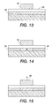
- Figure 13 shows the formation of the p-type region 34 under the gate metal and gate dielectric. This may be done by several methods including implantation.
- Figure 14 shows the formation of the n-type region 36.
- the gate receives an electrical connection to a fixed potential 48 shown in Figure 15 .
- the co-planar, gated diode may be employed in several different circuit applications, as discussed above.
Landscapes
- Thin Film Transistor (AREA)
- Metal-Oxide And Bipolar Metal-Oxide Semiconductor Integrated Circuits (AREA)
- Semiconductor Integrated Circuits (AREA)
Applications Claiming Priority (1)
| Application Number | Priority Date | Filing Date | Title |
|---|---|---|---|
| US12/358,171 US8384180B2 (en) | 2009-01-22 | 2009-01-22 | Gated co-planar poly-silicon thin film diode |
Publications (3)
| Publication Number | Publication Date |
|---|---|
| EP2211375A2 true EP2211375A2 (de) | 2010-07-28 |
| EP2211375A3 EP2211375A3 (de) | 2011-06-29 |
| EP2211375B1 EP2211375B1 (de) | 2019-04-24 |
Family
ID=42105875
Family Applications (1)
| Application Number | Title | Priority Date | Filing Date |
|---|---|---|---|
| EP10151256.4A Active EP2211375B1 (de) | 2009-01-22 | 2010-01-21 | Gate-gesteuerte Dünnfilmdiode, Verfahren zu deren Herstellung und Verfahren zu deren Anwendung |
Country Status (3)
| Country | Link |
|---|---|
| US (2) | US8384180B2 (de) |
| EP (1) | EP2211375B1 (de) |
| JP (1) | JP2010171428A (de) |
Families Citing this family (3)
| Publication number | Priority date | Publication date | Assignee | Title |
|---|---|---|---|---|
| US7955940B2 (en) * | 2009-09-01 | 2011-06-07 | International Business Machines Corporation | Silicon-on-insulator substrate with built-in substrate junction |
| US8618865B1 (en) | 2012-11-02 | 2013-12-31 | Palo Alto Research Center Incorporated | Capacitive imaging device with active pixels |
| US9224768B2 (en) * | 2013-08-05 | 2015-12-29 | Raytheon Company | Pin diode structure having surface charge suppression |
Citations (2)
| Publication number | Priority date | Publication date | Assignee | Title |
|---|---|---|---|---|
| EP0458570A1 (de) | 1990-05-21 | 1991-11-27 | Canon Kabushiki Kaisha | Diode und Halbleiterbauelement mit einer Diode |
| US20020117689A1 (en) | 2001-02-28 | 2002-08-29 | Hajime Akimoto | Field effect transistor and image display apparatus using the same |
Family Cites Families (9)
| Publication number | Priority date | Publication date | Assignee | Title |
|---|---|---|---|---|
| JP2773474B2 (ja) * | 1991-08-06 | 1998-07-09 | 日本電気株式会社 | 半導体装置 |
| JP2001068557A (ja) * | 1999-06-21 | 2001-03-16 | Matsushita Electric Ind Co Ltd | Pinダイオードを含む複合半導体装置、この装置の製造方法及びこの装置を用いた高周波装置 |
| GB0000510D0 (en) * | 2000-01-11 | 2000-03-01 | Koninkl Philips Electronics Nv | A charge pump circuit |
| JP2002118267A (ja) * | 2000-10-06 | 2002-04-19 | Hitachi Ltd | 半導体装置の製造方法および半導体装置 |
| JP2006060191A (ja) * | 2004-07-23 | 2006-03-02 | Seiko Epson Corp | 薄膜半導体装置及びその製造方法、電気光学装置、電子機器 |
| JP2006332237A (ja) * | 2005-05-25 | 2006-12-07 | Toshiba Matsushita Display Technology Co Ltd | 昇圧回路およびその駆動方法 |
| KR100747657B1 (ko) * | 2006-10-26 | 2007-08-08 | 삼성전자주식회사 | 매크로 및 마이크로 주파수 튜닝이 가능한 반도체 소자 및이를 갖는 안테나와 주파수 튜닝 회로 |
| US20080185596A1 (en) * | 2007-02-02 | 2008-08-07 | Tpo Displays Corp. | System for displaying images |
| JP2008253075A (ja) * | 2007-03-30 | 2008-10-16 | Tdk Corp | スイッチング電源装置 |
-
2009
- 2009-01-22 US US12/358,171 patent/US8384180B2/en not_active Expired - Fee Related
-
2010
- 2010-01-21 EP EP10151256.4A patent/EP2211375B1/de active Active
- 2010-01-22 JP JP2010011793A patent/JP2010171428A/ja active Pending
-
2013
- 2013-02-19 US US13/770,785 patent/US8871548B2/en active Active
Patent Citations (2)
| Publication number | Priority date | Publication date | Assignee | Title |
|---|---|---|---|---|
| EP0458570A1 (de) | 1990-05-21 | 1991-11-27 | Canon Kabushiki Kaisha | Diode und Halbleiterbauelement mit einer Diode |
| US20020117689A1 (en) | 2001-02-28 | 2002-08-29 | Hajime Akimoto | Field effect transistor and image display apparatus using the same |
Also Published As
| Publication number | Publication date |
|---|---|
| US8871548B2 (en) | 2014-10-28 |
| EP2211375B1 (de) | 2019-04-24 |
| JP2010171428A (ja) | 2010-08-05 |
| US20130164900A1 (en) | 2013-06-27 |
| US8384180B2 (en) | 2013-02-26 |
| US20100181573A1 (en) | 2010-07-22 |
| EP2211375A3 (de) | 2011-06-29 |
Similar Documents
| Publication | Publication Date | Title |
|---|---|---|
| EP0526897B1 (de) | Tunneleffektanordnung mit drei Elektroden | |
| EP2168163B1 (de) | Sperrschicht-feldeffekttransistor mit einer hyperabrupten sperrschicht | |
| US9553163B2 (en) | Metal-semiconductor-metal (MSM) heterojunction diode | |
| US8642453B2 (en) | Schottky barrier diode and method of forming a Schottky barrier diode | |
| US9577063B2 (en) | Bipolar transistor, band-gap reference circuit and virtual ground reference circuit and methods of fabricating thereof | |
| US20100059859A1 (en) | Varactor structure and method | |
| US20140346590A1 (en) | Semiconductor Device, Method of Manufacturing a Semiconductor Device and Integrated Circuit | |
| US8871548B2 (en) | Gated co-planar poly-silicon thin film diode | |
| US8742485B2 (en) | Inversion mode varactor | |
| US8004058B2 (en) | Schottky diode for high speed and radio frequency application | |
| US7474171B2 (en) | Method and apparatus for reducing dielectric charging in MEMS structures | |
| US10211347B2 (en) | Transcap device architecture with reduced control voltage and improved quality factor | |
| Buisman et al. | High-performance varactor diodes integrated in a silicon-on-glass technology | |
| Avenier et al. | Investigation of fully-and partially-depleted self-aligned SiGeC HBTs on thin film SOI | |
| US10622492B2 (en) | Variable capacitor flat-band voltage engineering | |
| US20190363198A1 (en) | Gallium-nitride-based transcaps for millimeter wave applications | |
| US20190326448A1 (en) | Back silicided variable capacitor devices |
Legal Events
| Date | Code | Title | Description |
|---|---|---|---|
| PUAI | Public reference made under article 153(3) epc to a published international application that has entered the european phase |
Free format text: ORIGINAL CODE: 0009012 |
|
| AK | Designated contracting states |
Kind code of ref document: A2 Designated state(s): AT BE BG CH CY CZ DE DK EE ES FI FR GB GR HR HU IE IS IT LI LT LU LV MC MK MT NL NO PL PT RO SE SI SK SM TR |
|
| AX | Request for extension of the european patent |
Extension state: AL BA RS |
|
| PUAL | Search report despatched |
Free format text: ORIGINAL CODE: 0009013 |
|
| AK | Designated contracting states |
Kind code of ref document: A3 Designated state(s): AT BE BG CH CY CZ DE DK EE ES FI FR GB GR HR HU IE IS IT LI LT LU LV MC MK MT NL NO PL PT RO SE SI SK SM TR |
|
| AX | Request for extension of the european patent |
Extension state: AL BA RS |
|
| 17P | Request for examination filed |
Effective date: 20111229 |
|
| 17Q | First examination report despatched |
Effective date: 20130913 |
|
| REG | Reference to a national code |
Ref country code: DE Ref legal event code: R079 Ref document number: 602010058381 Country of ref document: DE Free format text: PREVIOUS MAIN CLASS: H01L0021329000 Ipc: H01L0021330000 |
|
| GRAP | Despatch of communication of intention to grant a patent |
Free format text: ORIGINAL CODE: EPIDOSNIGR1 |
|
| STAA | Information on the status of an ep patent application or granted ep patent |
Free format text: STATUS: GRANT OF PATENT IS INTENDED |
|
| RIC1 | Information provided on ipc code assigned before grant |
Ipc: H01L 29/16 20060101ALN20181129BHEP Ipc: H01L 29/20 20060101ALN20181129BHEP Ipc: H01L 21/329 20060101AFI20181129BHEP Ipc: H01L 29/04 20060101ALN20181129BHEP Ipc: H01L 29/739 20060101ALI20181129BHEP |
|
| RIC1 | Information provided on ipc code assigned before grant |
Ipc: H01L 29/20 20060101ALN20181204BHEP Ipc: H01L 21/33 20060101AFI20181204BHEP Ipc: H01L 29/16 20060101ALN20181204BHEP Ipc: H01L 29/739 20060101ALI20181204BHEP Ipc: H01L 29/04 20060101ALN20181204BHEP |
|
| INTG | Intention to grant announced |
Effective date: 20181219 |
|
| GRAS | Grant fee paid |
Free format text: ORIGINAL CODE: EPIDOSNIGR3 |
|
| GRAA | (expected) grant |
Free format text: ORIGINAL CODE: 0009210 |
|
| STAA | Information on the status of an ep patent application or granted ep patent |
Free format text: STATUS: THE PATENT HAS BEEN GRANTED |
|
| AK | Designated contracting states |
Kind code of ref document: B1 Designated state(s): AT BE BG CH CY CZ DE DK EE ES FI FR GB GR HR HU IE IS IT LI LT LU LV MC MK MT NL NO PL PT RO SE SI SK SM TR |
|
| REG | Reference to a national code |
Ref country code: GB Ref legal event code: FG4D |
|
| REG | Reference to a national code |
Ref country code: CH Ref legal event code: EP |
|
| REG | Reference to a national code |
Ref country code: AT Ref legal event code: REF Ref document number: 1125138 Country of ref document: AT Kind code of ref document: T Effective date: 20190515 Ref country code: IE Ref legal event code: FG4D |
|
| REG | Reference to a national code |
Ref country code: DE Ref legal event code: R096 Ref document number: 602010058381 Country of ref document: DE |
|
| REG | Reference to a national code |
Ref country code: NL Ref legal event code: MP Effective date: 20190424 |
|
| REG | Reference to a national code |
Ref country code: LT Ref legal event code: MG4D |
|
| PG25 | Lapsed in a contracting state [announced via postgrant information from national office to epo] |
Ref country code: NL Free format text: LAPSE BECAUSE OF FAILURE TO SUBMIT A TRANSLATION OF THE DESCRIPTION OR TO PAY THE FEE WITHIN THE PRESCRIBED TIME-LIMIT Effective date: 20190424 |
|
| PG25 | Lapsed in a contracting state [announced via postgrant information from national office to epo] |
Ref country code: ES Free format text: LAPSE BECAUSE OF FAILURE TO SUBMIT A TRANSLATION OF THE DESCRIPTION OR TO PAY THE FEE WITHIN THE PRESCRIBED TIME-LIMIT Effective date: 20190424 Ref country code: PT Free format text: LAPSE BECAUSE OF FAILURE TO SUBMIT A TRANSLATION OF THE DESCRIPTION OR TO PAY THE FEE WITHIN THE PRESCRIBED TIME-LIMIT Effective date: 20190824 Ref country code: SE Free format text: LAPSE BECAUSE OF FAILURE TO SUBMIT A TRANSLATION OF THE DESCRIPTION OR TO PAY THE FEE WITHIN THE PRESCRIBED TIME-LIMIT Effective date: 20190424 Ref country code: FI Free format text: LAPSE BECAUSE OF FAILURE TO SUBMIT A TRANSLATION OF THE DESCRIPTION OR TO PAY THE FEE WITHIN THE PRESCRIBED TIME-LIMIT Effective date: 20190424 Ref country code: NO Free format text: LAPSE BECAUSE OF FAILURE TO SUBMIT A TRANSLATION OF THE DESCRIPTION OR TO PAY THE FEE WITHIN THE PRESCRIBED TIME-LIMIT Effective date: 20190724 Ref country code: HR Free format text: LAPSE BECAUSE OF FAILURE TO SUBMIT A TRANSLATION OF THE DESCRIPTION OR TO PAY THE FEE WITHIN THE PRESCRIBED TIME-LIMIT Effective date: 20190424 Ref country code: LT Free format text: LAPSE BECAUSE OF FAILURE TO SUBMIT A TRANSLATION OF THE DESCRIPTION OR TO PAY THE FEE WITHIN THE PRESCRIBED TIME-LIMIT Effective date: 20190424 |
|
| PG25 | Lapsed in a contracting state [announced via postgrant information from national office to epo] |
Ref country code: PL Free format text: LAPSE BECAUSE OF FAILURE TO SUBMIT A TRANSLATION OF THE DESCRIPTION OR TO PAY THE FEE WITHIN THE PRESCRIBED TIME-LIMIT Effective date: 20190424 Ref country code: BG Free format text: LAPSE BECAUSE OF FAILURE TO SUBMIT A TRANSLATION OF THE DESCRIPTION OR TO PAY THE FEE WITHIN THE PRESCRIBED TIME-LIMIT Effective date: 20190724 Ref country code: LV Free format text: LAPSE BECAUSE OF FAILURE TO SUBMIT A TRANSLATION OF THE DESCRIPTION OR TO PAY THE FEE WITHIN THE PRESCRIBED TIME-LIMIT Effective date: 20190424 Ref country code: GR Free format text: LAPSE BECAUSE OF FAILURE TO SUBMIT A TRANSLATION OF THE DESCRIPTION OR TO PAY THE FEE WITHIN THE PRESCRIBED TIME-LIMIT Effective date: 20190725 |
|
| REG | Reference to a national code |
Ref country code: AT Ref legal event code: MK05 Ref document number: 1125138 Country of ref document: AT Kind code of ref document: T Effective date: 20190424 |
|
| PG25 | Lapsed in a contracting state [announced via postgrant information from national office to epo] |
Ref country code: IS Free format text: LAPSE BECAUSE OF FAILURE TO SUBMIT A TRANSLATION OF THE DESCRIPTION OR TO PAY THE FEE WITHIN THE PRESCRIBED TIME-LIMIT Effective date: 20190824 |
|
| REG | Reference to a national code |
Ref country code: DE Ref legal event code: R097 Ref document number: 602010058381 Country of ref document: DE |
|
| PG25 | Lapsed in a contracting state [announced via postgrant information from national office to epo] |
Ref country code: EE Free format text: LAPSE BECAUSE OF FAILURE TO SUBMIT A TRANSLATION OF THE DESCRIPTION OR TO PAY THE FEE WITHIN THE PRESCRIBED TIME-LIMIT Effective date: 20190424 Ref country code: DK Free format text: LAPSE BECAUSE OF FAILURE TO SUBMIT A TRANSLATION OF THE DESCRIPTION OR TO PAY THE FEE WITHIN THE PRESCRIBED TIME-LIMIT Effective date: 20190424 Ref country code: AT Free format text: LAPSE BECAUSE OF FAILURE TO SUBMIT A TRANSLATION OF THE DESCRIPTION OR TO PAY THE FEE WITHIN THE PRESCRIBED TIME-LIMIT Effective date: 20190424 Ref country code: SK Free format text: LAPSE BECAUSE OF FAILURE TO SUBMIT A TRANSLATION OF THE DESCRIPTION OR TO PAY THE FEE WITHIN THE PRESCRIBED TIME-LIMIT Effective date: 20190424 Ref country code: CZ Free format text: LAPSE BECAUSE OF FAILURE TO SUBMIT A TRANSLATION OF THE DESCRIPTION OR TO PAY THE FEE WITHIN THE PRESCRIBED TIME-LIMIT Effective date: 20190424 Ref country code: RO Free format text: LAPSE BECAUSE OF FAILURE TO SUBMIT A TRANSLATION OF THE DESCRIPTION OR TO PAY THE FEE WITHIN THE PRESCRIBED TIME-LIMIT Effective date: 20190424 |
|
| PG25 | Lapsed in a contracting state [announced via postgrant information from national office to epo] |
Ref country code: IT Free format text: LAPSE BECAUSE OF FAILURE TO SUBMIT A TRANSLATION OF THE DESCRIPTION OR TO PAY THE FEE WITHIN THE PRESCRIBED TIME-LIMIT Effective date: 20190424 Ref country code: SM Free format text: LAPSE BECAUSE OF FAILURE TO SUBMIT A TRANSLATION OF THE DESCRIPTION OR TO PAY THE FEE WITHIN THE PRESCRIBED TIME-LIMIT Effective date: 20190424 |
|
| PLBE | No opposition filed within time limit |
Free format text: ORIGINAL CODE: 0009261 |
|
| STAA | Information on the status of an ep patent application or granted ep patent |
Free format text: STATUS: NO OPPOSITION FILED WITHIN TIME LIMIT |
|
| PG25 | Lapsed in a contracting state [announced via postgrant information from national office to epo] |
Ref country code: TR Free format text: LAPSE BECAUSE OF FAILURE TO SUBMIT A TRANSLATION OF THE DESCRIPTION OR TO PAY THE FEE WITHIN THE PRESCRIBED TIME-LIMIT Effective date: 20190424 |
|
| 26N | No opposition filed |
Effective date: 20200127 |
|
| PG25 | Lapsed in a contracting state [announced via postgrant information from national office to epo] |
Ref country code: SI Free format text: LAPSE BECAUSE OF FAILURE TO SUBMIT A TRANSLATION OF THE DESCRIPTION OR TO PAY THE FEE WITHIN THE PRESCRIBED TIME-LIMIT Effective date: 20190424 |
|
| PG25 | Lapsed in a contracting state [announced via postgrant information from national office to epo] |
Ref country code: MC Free format text: LAPSE BECAUSE OF FAILURE TO SUBMIT A TRANSLATION OF THE DESCRIPTION OR TO PAY THE FEE WITHIN THE PRESCRIBED TIME-LIMIT Effective date: 20190424 |
|
| REG | Reference to a national code |
Ref country code: CH Ref legal event code: PL |
|
| REG | Reference to a national code |
Ref country code: BE Ref legal event code: MM Effective date: 20200131 |
|
| PG25 | Lapsed in a contracting state [announced via postgrant information from national office to epo] |
Ref country code: LU Free format text: LAPSE BECAUSE OF NON-PAYMENT OF DUE FEES Effective date: 20200121 |
|
| PG25 | Lapsed in a contracting state [announced via postgrant information from national office to epo] |
Ref country code: BE Free format text: LAPSE BECAUSE OF NON-PAYMENT OF DUE FEES Effective date: 20200131 Ref country code: CH Free format text: LAPSE BECAUSE OF NON-PAYMENT OF DUE FEES Effective date: 20200131 Ref country code: LI Free format text: LAPSE BECAUSE OF NON-PAYMENT OF DUE FEES Effective date: 20200131 |
|
| PG25 | Lapsed in a contracting state [announced via postgrant information from national office to epo] |
Ref country code: IE Free format text: LAPSE BECAUSE OF NON-PAYMENT OF DUE FEES Effective date: 20200121 |
|
| PG25 | Lapsed in a contracting state [announced via postgrant information from national office to epo] |
Ref country code: MT Free format text: LAPSE BECAUSE OF FAILURE TO SUBMIT A TRANSLATION OF THE DESCRIPTION OR TO PAY THE FEE WITHIN THE PRESCRIBED TIME-LIMIT Effective date: 20190424 Ref country code: CY Free format text: LAPSE BECAUSE OF FAILURE TO SUBMIT A TRANSLATION OF THE DESCRIPTION OR TO PAY THE FEE WITHIN THE PRESCRIBED TIME-LIMIT Effective date: 20190424 |
|
| PG25 | Lapsed in a contracting state [announced via postgrant information from national office to epo] |
Ref country code: MK Free format text: LAPSE BECAUSE OF FAILURE TO SUBMIT A TRANSLATION OF THE DESCRIPTION OR TO PAY THE FEE WITHIN THE PRESCRIBED TIME-LIMIT Effective date: 20190424 |
|
| PGFP | Annual fee paid to national office [announced via postgrant information from national office to epo] |
Ref country code: GB Payment date: 20231219 Year of fee payment: 15 |
|
| PGFP | Annual fee paid to national office [announced via postgrant information from national office to epo] |
Ref country code: FR Payment date: 20231219 Year of fee payment: 15 |
|
| PGFP | Annual fee paid to national office [announced via postgrant information from national office to epo] |
Ref country code: DE Payment date: 20231219 Year of fee payment: 15 |
|
| REG | Reference to a national code |
Ref country code: DE Ref legal event code: R079 Ref document number: 602010058381 Country of ref document: DE Free format text: PREVIOUS MAIN CLASS: H01L0021330000 Ipc: H10D0012010000 |
|
| REG | Reference to a national code |
Ref country code: DE Ref legal event code: R119 Ref document number: 602010058381 Country of ref document: DE |
|
| GBPC | Gb: european patent ceased through non-payment of renewal fee |
Effective date: 20250121 |
|
| PG25 | Lapsed in a contracting state [announced via postgrant information from national office to epo] |
Ref country code: DE Free format text: LAPSE BECAUSE OF NON-PAYMENT OF DUE FEES Effective date: 20250801 |
|
| PG25 | Lapsed in a contracting state [announced via postgrant information from national office to epo] |
Ref country code: GB Free format text: LAPSE BECAUSE OF NON-PAYMENT OF DUE FEES Effective date: 20250121 |
|
| PG25 | Lapsed in a contracting state [announced via postgrant information from national office to epo] |
Ref country code: FR Free format text: LAPSE BECAUSE OF NON-PAYMENT OF DUE FEES Effective date: 20250131 |