EP2209645B1 - An inkjet print head with shared data lines - Google Patents
An inkjet print head with shared data lines Download PDFInfo
- Publication number
- EP2209645B1 EP2209645B1 EP07862050A EP07862050A EP2209645B1 EP 2209645 B1 EP2209645 B1 EP 2209645B1 EP 07862050 A EP07862050 A EP 07862050A EP 07862050 A EP07862050 A EP 07862050A EP 2209645 B1 EP2209645 B1 EP 2209645B1
- Authority
- EP
- European Patent Office
- Prior art keywords
- memory cell
- data signal
- print head
- data
- array
- Prior art date
- Legal status (The legal status is an assumption and is not a legal conclusion. Google has not performed a legal analysis and makes no representation as to the accuracy of the status listed.)
- Active
Links
- 238000000034 method Methods 0.000 claims description 20
- 238000004519 manufacturing process Methods 0.000 claims description 15
- 238000003491 array Methods 0.000 claims description 10
- 239000000758 substrate Substances 0.000 claims description 10
- 238000005516 engineering process Methods 0.000 claims description 9
- 239000004065 semiconductor Substances 0.000 claims description 8
- 239000010410 layer Substances 0.000 claims description 7
- 229910052710 silicon Inorganic materials 0.000 claims description 5
- 239000010703 silicon Substances 0.000 claims description 5
- 239000004020 conductor Substances 0.000 claims description 4
- 238000007667 floating Methods 0.000 claims description 3
- 239000004744 fabric Substances 0.000 claims description 2
- 239000004033 plastic Substances 0.000 claims description 2
- 239000002356 single layer Substances 0.000 claims description 2
- 239000002131 composite material Substances 0.000 claims 1
- XUIMIQQOPSSXEZ-UHFFFAOYSA-N Silicon Chemical compound [Si] XUIMIQQOPSSXEZ-UHFFFAOYSA-N 0.000 description 4
- 239000000463 material Substances 0.000 description 4
- 238000007639 printing Methods 0.000 description 4
- 238000006243 chemical reaction Methods 0.000 description 2
- 238000010367 cloning Methods 0.000 description 2
- 230000000295 complement effect Effects 0.000 description 2
- 238000007641 inkjet printing Methods 0.000 description 2
- 229910044991 metal oxide Inorganic materials 0.000 description 2
- 150000004706 metal oxides Chemical class 0.000 description 2
- 238000012986 modification Methods 0.000 description 2
- 230000004048 modification Effects 0.000 description 2
- 230000015572 biosynthetic process Effects 0.000 description 1
- 238000007664 blowing Methods 0.000 description 1
- 238000012937 correction Methods 0.000 description 1
- 238000011161 development Methods 0.000 description 1
- 239000012530 fluid Substances 0.000 description 1
- 239000011229 interlayer Substances 0.000 description 1
- 238000005259 measurement Methods 0.000 description 1
- 238000002844 melting Methods 0.000 description 1
- 230000008018 melting Effects 0.000 description 1
- 230000000135 prohibitive effect Effects 0.000 description 1
- 238000005507 spraying Methods 0.000 description 1
Images

Classifications
-
- B—PERFORMING OPERATIONS; TRANSPORTING
- B41—PRINTING; LINING MACHINES; TYPEWRITERS; STAMPS
- B41J—TYPEWRITERS; SELECTIVE PRINTING MECHANISMS, i.e. MECHANISMS PRINTING OTHERWISE THAN FROM A FORME; CORRECTION OF TYPOGRAPHICAL ERRORS
- B41J2/00—Typewriters or selective printing mechanisms characterised by the printing or marking process for which they are designed
- B41J2/005—Typewriters or selective printing mechanisms characterised by the printing or marking process for which they are designed characterised by bringing liquid or particles selectively into contact with a printing material
- B41J2/01—Ink jet
- B41J2/015—Ink jet characterised by the jet generation process
- B41J2/04—Ink jet characterised by the jet generation process generating single droplets or particles on demand
- B41J2/045—Ink jet characterised by the jet generation process generating single droplets or particles on demand by pressure, e.g. electromechanical transducers
- B41J2/04501—Control methods or devices therefor, e.g. driver circuits, control circuits
- B41J2/04541—Specific driving circuit
-
- B—PERFORMING OPERATIONS; TRANSPORTING
- B41—PRINTING; LINING MACHINES; TYPEWRITERS; STAMPS
- B41J—TYPEWRITERS; SELECTIVE PRINTING MECHANISMS, i.e. MECHANISMS PRINTING OTHERWISE THAN FROM A FORME; CORRECTION OF TYPOGRAPHICAL ERRORS
- B41J2/00—Typewriters or selective printing mechanisms characterised by the printing or marking process for which they are designed
- B41J2/005—Typewriters or selective printing mechanisms characterised by the printing or marking process for which they are designed characterised by bringing liquid or particles selectively into contact with a printing material
- B41J2/01—Ink jet
- B41J2/015—Ink jet characterised by the jet generation process
- B41J2/04—Ink jet characterised by the jet generation process generating single droplets or particles on demand
- B41J2/045—Ink jet characterised by the jet generation process generating single droplets or particles on demand by pressure, e.g. electromechanical transducers
- B41J2/04501—Control methods or devices therefor, e.g. driver circuits, control circuits
- B41J2/04521—Control methods or devices therefor, e.g. driver circuits, control circuits reducing number of signal lines needed
-
- B—PERFORMING OPERATIONS; TRANSPORTING
- B41—PRINTING; LINING MACHINES; TYPEWRITERS; STAMPS
- B41J—TYPEWRITERS; SELECTIVE PRINTING MECHANISMS, i.e. MECHANISMS PRINTING OTHERWISE THAN FROM A FORME; CORRECTION OF TYPOGRAPHICAL ERRORS
- B41J2/00—Typewriters or selective printing mechanisms characterised by the printing or marking process for which they are designed
- B41J2/005—Typewriters or selective printing mechanisms characterised by the printing or marking process for which they are designed characterised by bringing liquid or particles selectively into contact with a printing material
- B41J2/01—Ink jet
- B41J2/015—Ink jet characterised by the jet generation process
- B41J2/04—Ink jet characterised by the jet generation process generating single droplets or particles on demand
- B41J2/045—Ink jet characterised by the jet generation process generating single droplets or particles on demand by pressure, e.g. electromechanical transducers
- B41J2/04501—Control methods or devices therefor, e.g. driver circuits, control circuits
- B41J2/04586—Control methods or devices therefor, e.g. driver circuits, control circuits controlling heads of a type not covered by groups B41J2/04575 - B41J2/04585, or of an undefined type
-
- B—PERFORMING OPERATIONS; TRANSPORTING
- B41—PRINTING; LINING MACHINES; TYPEWRITERS; STAMPS
- B41J—TYPEWRITERS; SELECTIVE PRINTING MECHANISMS, i.e. MECHANISMS PRINTING OTHERWISE THAN FROM A FORME; CORRECTION OF TYPOGRAPHICAL ERRORS
- B41J2/00—Typewriters or selective printing mechanisms characterised by the printing or marking process for which they are designed
- B41J2/005—Typewriters or selective printing mechanisms characterised by the printing or marking process for which they are designed characterised by bringing liquid or particles selectively into contact with a printing material
- B41J2/01—Ink jet
- B41J2/21—Ink jet for multi-colour printing
- B41J2/2103—Features not dealing with the colouring process per se, e.g. construction of printers or heads, driving circuit adaptations
-
- B—PERFORMING OPERATIONS; TRANSPORTING
- B41—PRINTING; LINING MACHINES; TYPEWRITERS; STAMPS
- B41J—TYPEWRITERS; SELECTIVE PRINTING MECHANISMS, i.e. MECHANISMS PRINTING OTHERWISE THAN FROM A FORME; CORRECTION OF TYPOGRAPHICAL ERRORS
- B41J2202/00—Embodiments of or processes related to ink-jet or thermal heads
- B41J2202/01—Embodiments of or processes related to ink-jet heads
- B41J2202/13—Heads having an integrated circuit
Definitions
- An inkjet print head may contain nozzles or orifices for the ejection of printing fluid onto a printing medium. Nozzles are typically arranged in one or more arrays such that characters or images may be printed on a medium moving relative to the nozzle array.
- Print head attributes that may determine print head performance include ink drop volume, pen types, ink types, and column to column nozzle spacing. Data representing the inkjet attributes is stored with the print head and can be read by the inkjet printer during initialization.
- US2002/0140751 A1 describes a head substrate of a printing head detachably mounted on a printer main body, comprising plural external connection terminals individually receiving, from the exterior, a binary logic signals.
- the external terminals enable both recording and memory access.
- US 5956052 describes an image recording apparatus includes a recording unit integrally having an image forming recording head and a memory for storing a correction datum for correcting non-uniform image formation property.
- US2006/0256160 A1 describes an ink jet print head substrate capable of precisely blowing a fuse element to store data reliably.
- An interlayer insulating film formed over the fuse element is made of a material that has a lower melting point than the material of the fuse element and which forms a cavity therein by heat produced when the fuse elements is blown
- array parameters, shapes and other quantities and characteristics are not and need not be exact, but may be approximated and/or larger or smaller, as desired, reflecting process tolerances, conversion factors, rounding off, measurement error and the like and other factors known to those of skill in the art.
- FIG. 1 illustrates an inkjet print head that includes a plurality of data signal lines 110 configured to supply inkjet control voltages to a nozzle array and to supply random access addresses to a non-volatile memory cell array.
- the memory cell array may be used to store print head attributes such as column to column spacing, ink types, pen types, drop volume, ink availability, and other like attributes.
- non-volatile memory cells typically uses in excess of 14 to 16 masks but the fabrication of a nozzle array may require fewer than half as many masks. Developing a process technology to fabricate both the nozzle array and the non-volatile memory array together in a single print head can be cost prohibitive. Additionally, where the nozzle array and the memory array are fabricated separately, providing interconnects between the two arrays increases costs in manufacturing and debugging.
- Print heads which have devices that use fuses to store attributes require large silicon areas which may easily be visually examined to reverse engineer attribute data for cloning.
- the present disclosure inhibits cloning of print head attribute data by storing attribute data in non-volatile memory cells fabricated onto the same chip as the print head in a single fabrication technology with the nozzle arrays. Attribute data stored into non-volatile memory cells is less likely to be visually reverse engineered since the information is stored electronically on floating gates.
- the inkjet nozzle array 120 includes a plurality of nozzles wherein each nozzle in the array is configured to communicate with a data signal line 110 which may control the nozzle through variable voltages.
- the non-volatile memory cell array 140 includes a plurality of memory cells wherein each memory cell in the array is accessed through the data signal line shared with the nozzle array.
- the non-volatile memory cell can be an EPROM (Electrically Programmable Read Only Memory), Flash memory or another type of non-volatile memory.
- non-volatile memory cells of a chosen polarity need be programmed or written. Where a logical '1' is the chosen polarity of a programmed memory cell, logical '0' cells may remain unwritten. Thus only an address need be present at the memory cell array in order to write data to a non-volatile memory cell.
- the inkjet print head further comprises a data to address converter 130 configured to convert data on a data signal line into a random access address on multiple random address lines 150 labeled 'Address 1', through 'Address n+1' in FIG. 1 .
- a random access address as opposed to a sequential access address, allows access to a memory cell independent of the cell access prior to or following the access of the cell at the random access address.
- the data to address converter may further comprise a shift register configured to receive data from a data signal line connected to an input data pin.
- the data can be used for addressing the non-volatile attribute array.
- a data signal line may exist for every bit latched in the shift register. Every bit latched in the shift register becomes an address bit that may be applied to the memory array.
- a second shift register may be configured in an embodiment to receive data from a second data signal line connected to a second input data pin to enable addressing a second portion of the non-volatile attribute array.
- the data to address converter may comprise transistor logic configured to generate a plurality of random access address lines.
- a single data line may generate two address lines by using Boolean true and complement line generation.
- Two address lines may generate four address lines by all possible combinations of the Boolean true and complement of the two address lines. Therefore, 2 N possible address lines may be generated where N is equal to the number of data lines entering the data to address converter.
- the non-volatile attribute memory cell array may further comprise 64 cells to 128 cells.
- An array may also be split into several physically discrete though logically adjacent smaller arrays to utilize existing space in the print head silicon. Arrays may be rectangular or square to fit die space requirements.
- One result of the present disclosure is that non-volatile memory arrays may be added to the print head without any increase in silicon area above that needed for the nozzle arrays and print head control.
- Programming voltages may be generated off the print head and read currents may be sensed off the print head.
- support circuitry may be minimized for the memory cell array.
- the arrays are scalable to a larger number of memory cells by adding address lines for future advanced implementations.
- An embodiment of the array may include multiple columns of NMOS (N-channel Metal Oxide Semiconductor) devices in series with a non-volatile n-channel memory device. Therefore, an inkjet print head may include only active devices characterized as NMOS devices with no PMOS (P-channel Metal Oxide Semiconductor) devices at all. Additionally, the non-volatile attribute memory cell array may include a covering over each attribute memory cell configured to prevent ultraviolet light erasure of the data stored on the non-volatile memory cell. However, erasure and programming of the array may be possible at wafer-sort prior to application of the cover.
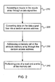
- the method includes accessing a nozzle in the nozzle array through a data signal line as in step 210 depicted in FIG. 2 .
- Data on the data signal line is converted into a random access address as in step 220.
- Memory cells in the attribute memory array are addressed through the random access address, as in step 230.
- a read or a write of the memory cell is performed as in step 240.
- the data signal line used to control a nozzle in the nozzle array is the same data signal line used to address a memory cell after the conversion of data to a random access address.
- One embodiment for sharing the data signal line between the nozzle array and the memory array includes latching data signals into a shift register wherein each latched signal has a corresponding signal line.
- the data signal lines from the shift register are applied to the memory cell array to access a memory cell at random for either a read or a write.
- the shift register effectively converts incoming data into a random access address. No data is necessary to address the nonvolatile memory array since the memory cell array only needs an address to program a binary '1' or a '0'.
- An attribute memory cell can be read by sensing a voltage or a current from a column in the memory cell array associated with a memory cell on that column at a row address.
- an embodiment for writing an attribute memory cell includes driving a variable voltage pulse and a variable current source into a column associated with a data signal line and a memory cell. Reading and writing a memory cell may be done using support circuitry located on or off the print head.
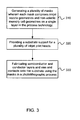
- FIG. 3 A method of making an inkjet print head in a single process technology is depicted in FIG. 3 .
- Masks are generated wherein each mask may comprise inkjet nozzle geometries and non-volatile memory cell geometries on a single layer in the process technology as in step 310.
- a substrate support is provided as in step 320 for the fabrication of multiple inkjet print heads as may be stepped on a single semiconductor wafer.
- a substrate may be cut from a silicon ingot, a glassy material, formed from a plastic, or a fabric material.
- Substrates provide a substantially flat surface on which to form the active semiconductor devices.
- the substrates used can be electrically non-conductive or may include an electrically non-conductive layer and may vary in thickness depending on the mechanical strength needed and the cost targeted in manufacturing.
- Semiconductor layers, conductor layers, associated vias and contacts can be fabricated onto the substrate as in step 330 using the masks in a photolithographic process.
- the method of making an inkjet print head further includes generating masks having data signal lines shared between a nozzle array and a memory cell array. Since the fabrication technology for the non-volatile memory array has been optimized to the masks required for the nozzle array, fewer than 10 masks may be all that are needed to fabricate the memory cell array.
- a single process technology may include fabricating the semiconductor and conductor layers from a single master set of photolithographic masks configured to produce at least one complete print head.
Description
- One of the areas of continued progress of inkjet printing is that of print heads. Development is ongoing and is working towards improved print speeds, quality and resolution, versatility in handling different ink bases and viscosity, robustness of the print heads for industrial applications, and improved width of printing swathes. Manufacturers have reduced printer prices by incorporating much of the actual print head into the cartridge itself. The manufacturers believe that since the print head is the part of the printer that is most likely to wear out, replacing it every time the cartridge is replaced can increase the life of the printer. Modem inkjet printing is performed with a self-contained print head that includes an ink reservoir, complete with inkwell, spraying mechanism, and nozzles that can be controlled accurately. An inkjet print head may contain nozzles or orifices for the ejection of printing fluid onto a printing medium. Nozzles are typically arranged in one or more arrays such that characters or images may be printed on a medium moving relative to the nozzle array. Print head attributes that may determine print head performance include ink drop volume, pen types, ink types, and column to column nozzle spacing. Data representing the inkjet attributes is stored with the print head and can be read by the inkjet printer during initialization.
-
US2002/0140751 A1 describes a head substrate of a printing head detachably mounted on a printer main body, comprising plural external connection terminals individually receiving, from the exterior, a binary logic signals. The external terminals enable both recording and memory access. -
US 5956052 describes an image recording apparatus includes a recording unit integrally having an image forming recording head and a memory for storing a correction datum for correcting non-uniform image formation property. -
US2006/0256160 A1 describes an ink jet print head substrate capable of precisely blowing a fuse element to store data reliably. An interlayer insulating film formed over the fuse element is made of a material that has a lower melting point than the material of the fuse element and which forms a cavity therein by heat produced when the fuse elements is blown - Aspects of the present invention are set out in the appended claims.
-
-
FIG. 1 depicts elements of an inkjet print head in accordance with an embodiment; -
FIG. 2 depicts an embodiment of a method for using an inkjet print head having a nozzle array and a corresponding non-volatile memory cell array; and -
FIG. 3 depicts an embodiment of a method of making an inkjet print head in a single process technology. - In describing embodiments of the present invention, the following terminology will be used.
- The singular forms "a," "an," and "the" include plural referents unless the context clearly dictates otherwise. Thus, for example, reference to "a device" includes reference to one or more of such devices.
- As used herein, array parameters, shapes and other quantities and characteristics are not and need not be exact, but may be approximated and/or larger or smaller, as desired, reflecting process tolerances, conversion factors, rounding off, measurement error and the like and other factors known to those of skill in the art.
- Reference will now be made to the exemplary embodiments illustrated, and specific language will be used herein to describe the same. It will nevertheless be understood that no limitation of the scope of the invention is thereby intended.
-
FIG. 1 illustrates an inkjet print head that includes a plurality ofdata signal lines 110 configured to supply inkjet control voltages to a nozzle array and to supply random access addresses to a non-volatile memory cell array. As a result, extra data signal lines are not needed for the memory cell array. The memory cell array may be used to store print head attributes such as column to column spacing, ink types, pen types, drop volume, ink availability, and other like attributes. - The fabrication of non-volatile memory cells typically uses in excess of 14 to 16 masks but the fabrication of a nozzle array may require fewer than half as many masks. Developing a process technology to fabricate both the nozzle array and the non-volatile memory array together in a single print head can be cost prohibitive. Additionally, where the nozzle array and the memory array are fabricated separately, providing interconnects between the two arrays increases costs in manufacturing and debugging.
- Print heads which have devices that use fuses to store attributes require large silicon areas which may easily be visually examined to reverse engineer attribute data for cloning. The present disclosure inhibits cloning of print head attribute data by storing attribute data in non-volatile memory cells fabricated onto the same chip as the print head in a single fabrication technology with the nozzle arrays. Attribute data stored into non-volatile memory cells is less likely to be visually reverse engineered since the information is stored electronically on floating gates.
- The
inkjet nozzle array 120 includes a plurality of nozzles wherein each nozzle in the array is configured to communicate with adata signal line 110 which may control the nozzle through variable voltages. The non-volatilememory cell array 140 includes a plurality of memory cells wherein each memory cell in the array is accessed through the data signal line shared with the nozzle array. The non-volatile memory cell can be an EPROM (Electrically Programmable Read Only Memory), Flash memory or another type of non-volatile memory. - Only non-volatile memory cells of a chosen polarity need be programmed or written. Where a logical '1' is the chosen polarity of a programmed memory cell, logical '0' cells may remain unwritten. Thus only an address need be present at the memory cell array in order to write data to a non-volatile memory cell.
- The inkjet print head further comprises a data to address
converter 130 configured to convert data on a data signal line into a random access address on multiplerandom address lines 150 labeled 'Address 1', through 'Address n+1' inFIG. 1 . A random access address, as opposed to a sequential access address, allows access to a memory cell independent of the cell access prior to or following the access of the cell at the random access address. - The data to address converter may further comprise a shift register configured to receive data from a data signal line connected to an input data pin. The data can be used for addressing the non-volatile attribute array. A data signal line may exist for every bit latched in the shift register. Every bit latched in the shift register becomes an address bit that may be applied to the memory array.
- To improve efficiency, a second shift register may be configured in an embodiment to receive data from a second data signal line connected to a second input data pin to enable addressing a second portion of the non-volatile attribute array. The more shift registers used in an embodiment, the less shifting of data is required to program the shift register and thus the converter becomes more efficient. In an alternate embodiment, the data to address converter may comprise transistor logic configured to generate a plurality of random access address lines. A single data line may generate two address lines by using Boolean true and complement line generation. Two address lines may generate four address lines by all possible combinations of the Boolean true and complement of the two address lines. Therefore, 2N possible address lines may be generated where N is equal to the number of data lines entering the data to address converter.
- In other embodiments, the non-volatile attribute memory cell array may further comprise 64 cells to 128 cells. An array may also be split into several physically discrete though logically adjacent smaller arrays to utilize existing space in the print head silicon. Arrays may be rectangular or square to fit die space requirements. One result of the present disclosure is that non-volatile memory arrays may be added to the print head without any increase in silicon area above that needed for the nozzle arrays and print head control.
- Programming voltages may be generated off the print head and read currents may be sensed off the print head. Thus, support circuitry may be minimized for the memory cell array. Furthermore, the arrays are scalable to a larger number of memory cells by adding address lines for future advanced implementations.
- An embodiment of the array may include multiple columns of NMOS (N-channel Metal Oxide Semiconductor) devices in series with a non-volatile n-channel memory device. Therefore, an inkjet print head may include only active devices characterized as NMOS devices with no PMOS (P-channel Metal Oxide Semiconductor) devices at all. Additionally, the non-volatile attribute memory cell array may include a covering over each attribute memory cell configured to prevent ultraviolet light erasure of the data stored on the non-volatile memory cell. However, erasure and programming of the array may be possible at wafer-sort prior to application of the cover.
- A method of using an inkjet print head having a nozzle array and a corresponding attribute non-volatile memory cell array will now be discussed. The method includes accessing a nozzle in the nozzle array through a data signal line as in
step 210 depicted inFIG. 2 . Data on the data signal line is converted into a random access address as instep 220. Memory cells in the attribute memory array are addressed through the random access address, as instep 230. A read or a write of the memory cell is performed as instep 240. The data signal line used to control a nozzle in the nozzle array is the same data signal line used to address a memory cell after the conversion of data to a random access address. One embodiment for sharing the data signal line between the nozzle array and the memory array includes latching data signals into a shift register wherein each latched signal has a corresponding signal line. The data signal lines from the shift register are applied to the memory cell array to access a memory cell at random for either a read or a write. Thus, the shift register effectively converts incoming data into a random access address. No data is necessary to address the nonvolatile memory array since the memory cell array only needs an address to program a binary '1' or a '0'. - An attribute memory cell can be read by sensing a voltage or a current from a column in the memory cell array associated with a memory cell on that column at a row address. Likewise an embodiment for writing an attribute memory cell includes driving a variable voltage pulse and a variable current source into a column associated with a data signal line and a memory cell. Reading and writing a memory cell may be done using support circuitry located on or off the print head.
- A method of making an inkjet print head in a single process technology is depicted in
FIG. 3 . Masks are generated wherein each mask may comprise inkjet nozzle geometries and non-volatile memory cell geometries on a single layer in the process technology as instep 310. A substrate support is provided as instep 320 for the fabrication of multiple inkjet print heads as may be stepped on a single semiconductor wafer. A substrate may be cut from a silicon ingot, a glassy material, formed from a plastic, or a fabric material. Substrates provide a substantially flat surface on which to form the active semiconductor devices. The substrates used can be electrically non-conductive or may include an electrically non-conductive layer and may vary in thickness depending on the mechanical strength needed and the cost targeted in manufacturing. Semiconductor layers, conductor layers, associated vias and contacts can be fabricated onto the substrate as instep 330 using the masks in a photolithographic process. The method of making an inkjet print head further includes generating masks having data signal lines shared between a nozzle array and a memory cell array. Since the fabrication technology for the non-volatile memory array has been optimized to the masks required for the nozzle array, fewer than 10 masks may be all that are needed to fabricate the memory cell array. A single process technology may include fabricating the semiconductor and conductor layers from a single master set of photolithographic masks configured to produce at least one complete print head. - It is to be understood that the above-referenced arrangements are only illustrative of the application for the principles of the present invention. Numerous modifications and alternative arrangements can be devised without departing from the scope of the present invention. While the present invention has been shown in the drawings and fully described above with particularity and detail in connection with what is presently deemed to be the most practical and preferred embodiment(s) of the invention, it will be apparent to those of ordinary skill in the art that numerous modifications can be made without departing from the principles and concepts of the invention as set forth herein.
Claims (18)
- An inkjet print head, comprising:a plurality of data signal lines (110); andan inkjet nozzle array (120) having a plurality of nozzles wherein each nozzle in the array is configured to communicate with a data signal line from the plurality of data signal lines (110);the inkjet print head characterised by:a non-volatile attribute memory cell array (140), each memory cell in the array storing data electronically on one or more floating gates; anda data to address converter (130) configured to convert data from a data signal line into a random access address on a plurality of random access address lines;wherein the plurality of data signal lines (110) are configured to supply inkjet control voltages and non-volatile memory cell random access addresses, andwherein each memory cell in the array is accessible through a data signal line from the plurality of data signal lines (110) shared with the nozzle array (120).
- An inkjet print head as in claim 1, wherein the data to address converter (130) further comprises:a first shift register configured to receive data from a first input data pin for a first data signal line and to address a portion of the non-volatile attribute array; anda second shift register configured to receive data from a second input data pin for a second data signal line and to address a remaining portion of the non-volatile attribute array.
- An inkjet print head as in claim 1, wherein the data to address converter (130) further comprises transistor logic configured to generate a plurality of random access address signals.
- An inkjet print head as in claim 1, wherein the non-volatile attribute memory cell array (140) further comprises 64 cells to 128 cells.
- An inkjet print head as in claim 1, wherein the non-volatile attribute memory cell array (140) further comprises multiple columns of n-channel devices in series with a non-volatile n-channel memory device.
- An inkjet print head as in claim 1, wherein the non-volatile attribute memory cell array (140) further comprises a cover over the non-volatile attribute memory cell array configured to prevent ultraviolet light erasure of the data stored on the non-volatile memory cell.
- An inkjet print head as in claim 1, wherein the non-volatile memory cells are configured to store inkjet data attributes selected from the group consisting of column to column spacing, ink types, pen types, drop volume, and ink availability.
- An inkjet print head as in claim 1, wherein the non-volatile attribute memory cell array (140) is split into several physically discrete arrays that are logically adjacent.
- A method of using an inkjet print head having a nozzle array (120) and a corresponding attribute non-volatile memory cell array (140), comprising:accessing (210) a nozzle in the nozzle array 9120) through a data signal line, the data signal line comprising one of a plurality of data signal lines (110) configured to supply inkjet control voltages;the method characterised by the steps of:converting (220) data on the data signal line into a random access address, wherein the plurality of data signal lines (110) are further configured to supply non-volatile memory cell random access addresses;addressing (230) a memory cell in the attribute memory array (140) through the random access address; andperforming (240) one of a read and a write of the memory cell using random access addresses converted from the data signal line, each memory cell in the array (140) storing data electronically on one or more floating gates and being accessible through a data signal line from the plurality of data signal lines (110) shared with the nozzle array (120).
- A method of using an inkjet print head as in 9, wherein converting data on the data signal line into a random access address further comprises:latching a plurality of data signals into a shift register wherein each latched signal has a corresponding data signal line;applying data from the plurality of data signal lines as converted by the shift register to the memory cell array; andreading an attribute memory cell in the memory cell array (140) at a random access address defined by the data signal lines.
- A method of using an inkjet print head as in claim 9, wherein converting data on the data signal line into a random access address further comprises:latching a plurality of data signals into a shift register wherein each latched signal has a corresponding data signal line;applying data from the plurality of data signal lines as converted by the shift register to the memory cell array; andwriting an attribute memory cell in the memory cell array (140) at a random access address defined by the data signal lines.
- A method of using an inkjet print head as in claim 10, wherein reading an attribute memory cell further comprises sensing one of a voltage and a current of a column in the memory cell array associated with a random access address of a memory cell.
- A method of using an inkjet print head as in claim 11, wherein writing an attribute memory cell further comprises driving a variable voltage pulse and a variable current source into a column associated with a data signal line and a memory cell.
- A method of making an inkjet print head in a single process technology, comprising:generating (310) a plurality of masks wherein each mask comprises inkjet nozzle geometries and non-volatile memory cell geometries on a single layer in the process technology;providing (320) a substrate support for a plurality of inkjet print heads; andfabricating (330) semiconductor layers, conductor layers, vias and contacts onto the substrate using the plurality of masks in a photolithographic process;the method characterised in that:the plurality of masks have a plurality of data signal lines (110) shared between a nozzle array (120) and a memory cell array (140), andthe non-volatile memory cell geometries are arranged to produce multiple columns of n-channel devices in series with a non-volatile n-channel memory device.
- A method of making an inkjet print head as in claim 14, further comprising providing a plurality of masks less than or equal to 10 in quantity.
- A method of making an inkjet print head as in claim 14, further comprising providing a substrate selected from the group consisting of silicon, plastic, fabric, and composites thereof.
- A method of making an inkjet print head as in claim 14, further comprising fabricating the semiconductor and conductor layers from a single master set of photolithographic masks configured to produce at least one complete print head.
- A method of making an inkjet print head as in claim 14, further comprising providing a plurality of masks wherein the memory cell array is split into several physically discrete arrays arranged to utilise space not used for the inkjet nozzle geometries.
Priority Applications (1)
| Application Number | Priority Date | Filing Date | Title |
|---|---|---|---|
| PL07862050T PL2209645T3 (en) | 2007-11-14 | 2007-11-14 | An inkjet print head with shared data lines |
Applications Claiming Priority (1)
| Application Number | Priority Date | Filing Date | Title |
|---|---|---|---|
| PCT/US2007/023991 WO2009064271A1 (en) | 2007-11-14 | 2007-11-14 | An inkjet print head with shared data lines |
Publications (3)
| Publication Number | Publication Date |
|---|---|
| EP2209645A1 EP2209645A1 (en) | 2010-07-28 |
| EP2209645A4 EP2209645A4 (en) | 2010-12-15 |
| EP2209645B1 true EP2209645B1 (en) | 2013-03-27 |
Family
ID=40638964
Family Applications (1)
| Application Number | Title | Priority Date | Filing Date |
|---|---|---|---|
| EP07862050A Active EP2209645B1 (en) | 2007-11-14 | 2007-11-14 | An inkjet print head with shared data lines |
Country Status (11)
| Country | Link |
|---|---|
| US (2) | US9707752B2 (en) |
| EP (1) | EP2209645B1 (en) |
| CN (1) | CN101868356B (en) |
| AR (1) | AR069331A1 (en) |
| CL (1) | CL2008003388A1 (en) |
| DK (1) | DK2209645T3 (en) |
| ES (1) | ES2403304T3 (en) |
| PL (1) | PL2209645T3 (en) |
| PT (1) | PT2209645E (en) |
| TW (1) | TWI444301B (en) |
| WO (1) | WO2009064271A1 (en) |
Families Citing this family (28)
| Publication number | Priority date | Publication date | Assignee | Title |
|---|---|---|---|---|
| US9707752B2 (en) * | 2007-11-14 | 2017-07-18 | Hewlett-Packard Development Company, L.P. | Inkjet print head with shared data lines |
| WO2015108527A1 (en) * | 2014-01-17 | 2015-07-23 | Hewlett-Packard Development Company, L.P. | Addressing an eprom on a printhead |
| WO2015160350A1 (en) * | 2014-04-17 | 2015-10-22 | Hewlett-Packard Development Company, L.P. | Addressing an eprom on a printhead |
| JP6417588B2 (en) * | 2014-10-16 | 2018-11-07 | セイコーエプソン株式会社 | Nozzle array drive data conversion device and droplet discharge device |
| CN107073940B (en) * | 2014-10-29 | 2018-11-30 | 惠普发展公司,有限责任合伙企业 | Print head assembly, method and print system for the control of print head injection signal |
| CN104952485B (en) * | 2014-11-28 | 2019-07-19 | 珠海艾派克微电子有限公司 | A kind of resistance switching circuit, storage circuit and consumable chip |
| US10173420B2 (en) | 2015-07-30 | 2019-01-08 | Hewlett-Packard Development Company, L.P. | Printhead assembly |
| JP6851757B2 (en) * | 2016-09-16 | 2021-03-31 | 東芝テック株式会社 | Inkjet head and inkjet printer |
| HUE048918T2 (en) * | 2016-10-06 | 2020-08-28 | Hewlett Packard Development Co | Input control signals propagated over signal paths |
| CN113276561B (en) | 2017-01-31 | 2022-10-11 | 惠普发展公司,有限责任合伙企业 | Memory bank device for fluid ejection sheet, fluid ejection sheet and fluid cartridge |
| WO2019009903A1 (en) | 2017-07-06 | 2019-01-10 | Hewlett-Packard Development Company, L.P. | Data lines to fluid ejection devices |
| DE112017007727T5 (en) | 2017-07-06 | 2020-03-19 | Hewlett-Packard Development Company, L.P. | DECODER FOR STORAGE OF FLUID EMISSION DEVICES |
| PL3915791T3 (en) * | 2017-07-06 | 2023-11-20 | Hewlett-Packard Development Company, L.P. | Selectors for nozzles and memory elements |
| EP3688638B1 (en) * | 2018-12-03 | 2023-01-04 | Hewlett-Packard Development Company, L.P. | Logic circuitry package |
| US11787173B2 (en) | 2019-02-06 | 2023-10-17 | Hewlett-Packard Development Company, L.P. | Print component with memory circuit |
| MX2021008849A (en) | 2019-02-06 | 2021-09-08 | Hewlett Packard Development Co | Print component with memory circuit. |
| JP7146103B2 (en) * | 2019-02-06 | 2022-10-03 | ヒューレット-パッカード デベロップメント カンパニー エル.ピー. | pull down device |
| EP3717253B1 (en) * | 2019-02-06 | 2022-05-11 | Hewlett-Packard Development Company, L.P. | Memories of fluidic dies |
| MX2021009122A (en) | 2019-02-06 | 2021-09-08 | Hewlett Packard Development Co | Communicating print component. |
| AU2019428183B2 (en) | 2019-02-06 | 2023-01-19 | Hewlett-Packard Development Company, L.P. | Communicating print component |
| US11331911B2 (en) * | 2019-02-06 | 2022-05-17 | Hewlett-Packard Development Company, L.P. | Die for a printhead |
| EP3845386B1 (en) | 2019-02-06 | 2024-04-03 | Hewlett-Packard Development Company, L.P. | Multiple circuits coupled to an interface |
| HUE055328T2 (en) * | 2019-02-06 | 2021-11-29 | Hewlett Packard Development Co | Integrated circuits including memory cells |
| CN116039245A (en) | 2019-02-06 | 2023-05-02 | 惠普发展公司,有限责任合伙企业 | Integrated circuit and method of operation thereof |
| MX2021008895A (en) | 2019-02-06 | 2021-08-19 | Hewlett Packard Development Co | Communicating print component. |
| US11590753B2 (en) | 2019-04-19 | 2023-02-28 | Hewlett-Packard Development Company, L.P. | Fluid ejection devices including a memory |
| ES2955911T3 (en) * | 2019-04-19 | 2023-12-11 | Hewlett Packard Development Co | Ink jet cartridge comprising a print head including an integrated circuit comprising a fluid ejection device, a first memory and a second memory, and a corresponding method |
| ES2924517T3 (en) * | 2019-04-19 | 2022-10-07 | Hewlett Packard Development Co | Fluid ejection devices that include a memory |
Family Cites Families (25)
| Publication number | Priority date | Publication date | Assignee | Title |
|---|---|---|---|---|
| US4281401A (en) * | 1979-11-23 | 1981-07-28 | Texas Instruments Incorporated | Semiconductor read/write memory array having high speed serial shift register access |
| US4922137A (en) * | 1988-05-17 | 1990-05-01 | Eastman Kodak Company | Programmable sequence generator |
| US4930107A (en) * | 1988-08-08 | 1990-05-29 | Altera Corporation | Method and apparatus for programming and verifying programmable elements in programmable devices |
| DE69033001T2 (en) * | 1989-10-05 | 1999-09-09 | Canon Kk | Imaging device |
| US5363134A (en) * | 1992-05-20 | 1994-11-08 | Hewlett-Packard Corporation | Integrated circuit printhead for an ink jet printer including an integrated identification circuit |
| US5757394A (en) * | 1995-09-27 | 1998-05-26 | Lexmark International, Inc. | Ink jet print head identification circuit with programmed transistor array |
| US6022094A (en) * | 1995-09-27 | 2000-02-08 | Lexmark International, Inc. | Memory expansion circuit for ink jet print head identification circuit |
| DE69935958T2 (en) * | 1998-10-27 | 2008-01-10 | Canon K.K. | Head carrier layer, printhead with data storage and printing device |
| JP4314702B2 (en) * | 1998-11-26 | 2009-08-19 | セイコーエプソン株式会社 | Printing apparatus, writing method, and printer |
| JP3709470B2 (en) * | 2000-02-29 | 2005-10-26 | 株式会社沖データ | Image recording device |
| JP2002067290A (en) | 2000-08-31 | 2002-03-05 | Canon Inc | Recording head, recorder and method of transmitting data between recording head and recorder |
| TW514604B (en) * | 2001-08-10 | 2002-12-21 | Int United Technology Co Ltd | Recognition circuit for an ink jet printer |
| JP3830486B2 (en) | 2002-04-03 | 2006-10-04 | 株式会社オージーエー | Exercise aid |
| US20040095409A1 (en) * | 2002-11-11 | 2004-05-20 | Hung-Lieh Hu | Apparatus and method for determining status of inkjet print head identification circuit |
| CN101428474B (en) * | 2003-05-01 | 2013-01-23 | 奥布吉特几何有限公司 | Rapid prototyping apparatus |
| US7311385B2 (en) * | 2003-11-12 | 2007-12-25 | Lexmark International, Inc. | Micro-fluid ejecting device having embedded memory device |
| TWI237597B (en) * | 2004-01-29 | 2005-08-11 | Int United Technology Co Ltd | Inkjet printer's recognize circuit |
| US7497536B2 (en) * | 2004-04-19 | 2009-03-03 | Hewlett-Packard Development Company, L.P. | Fluid ejection device |
| JP4047328B2 (en) * | 2004-12-24 | 2008-02-13 | キヤノン株式会社 | Liquid storage container, liquid supply system and recording apparatus using the container, and circuit board for the container |
| JP2006327180A (en) * | 2005-04-28 | 2006-12-07 | Canon Inc | Substrate for inkjet recording head, inkjet recording head, inkjet recording device and method for manufacturing substrate for inkjet recording head |
| US7345915B2 (en) * | 2005-10-31 | 2008-03-18 | Hewlett-Packard Development Company, L.P. | Modified-layer EPROM cell |
| US8128205B2 (en) * | 2005-10-31 | 2012-03-06 | Hewlett-Packard Development Company, L.P. | Fluid ejection device |
| US7209384B1 (en) * | 2005-12-08 | 2007-04-24 | Juhan Kim | Planar capacitor memory cell and its applications |
| US20070236519A1 (en) * | 2006-03-31 | 2007-10-11 | Edelen John G | Multi-Level Memory for Micro-Fluid Ejection Heads |
| US9707752B2 (en) * | 2007-11-14 | 2017-07-18 | Hewlett-Packard Development Company, L.P. | Inkjet print head with shared data lines |
-
2007
- 2007-11-14 US US12/739,076 patent/US9707752B2/en active Active
- 2007-11-14 EP EP07862050A patent/EP2209645B1/en active Active
- 2007-11-14 PT PT78620507T patent/PT2209645E/en unknown
- 2007-11-14 ES ES07862050T patent/ES2403304T3/en active Active
- 2007-11-14 WO PCT/US2007/023991 patent/WO2009064271A1/en active Application Filing
- 2007-11-14 CN CN200780101551.5A patent/CN101868356B/en active Active
- 2007-11-14 PL PL07862050T patent/PL2209645T3/en unknown
- 2007-11-14 DK DK07862050.7T patent/DK2209645T3/en active
-
2008
- 2008-11-13 TW TW097143867A patent/TWI444301B/en active
- 2008-11-14 AR ARP080104984A patent/AR069331A1/en active IP Right Grant
- 2008-11-14 CL CL2008003388A patent/CL2008003388A1/en unknown
-
2016
- 2016-11-22 US US15/359,049 patent/US9987841B2/en active Active
Also Published As
| Publication number | Publication date |
|---|---|
| EP2209645A1 (en) | 2010-07-28 |
| WO2009064271A1 (en) | 2009-05-22 |
| US20100302293A1 (en) | 2010-12-02 |
| CN101868356A (en) | 2010-10-20 |
| DK2209645T3 (en) | 2013-05-13 |
| AR069331A1 (en) | 2010-01-13 |
| TW200932559A (en) | 2009-08-01 |
| US20170072687A1 (en) | 2017-03-16 |
| PT2209645E (en) | 2013-04-09 |
| EP2209645A4 (en) | 2010-12-15 |
| CL2008003388A1 (en) | 2009-03-06 |
| ES2403304T3 (en) | 2013-05-17 |
| TWI444301B (en) | 2014-07-11 |
| PL2209645T3 (en) | 2013-10-31 |
| US9707752B2 (en) | 2017-07-18 |
| CN101868356B (en) | 2014-01-01 |
| US9987841B2 (en) | 2018-06-05 |
Similar Documents
| Publication | Publication Date | Title |
|---|---|---|
| EP2209645B1 (en) | An inkjet print head with shared data lines | |
| US8882217B2 (en) | Printhead assembly including memory elements | |
| US7311385B2 (en) | Micro-fluid ejecting device having embedded memory device | |
| CN112976811A (en) | Circuit for memory element and nozzle and apparatus for printing | |
| CN110234509B (en) | Setting memory banks and select registers | |
| JP5426581B2 (en) | Semiconductor memory device | |
| US20230074257A1 (en) | Integrated circuits including customization bits | |
| CN112976813B (en) | Storage body for fluid ejection sheet, fluid cartridge, and print cartridge | |
| CA3126606C (en) | Integrated circuits including customization bits | |
| EP4334798A1 (en) | Integrated circuits including high-voltage high-power and high-voltage low-power supply nodes |
Legal Events
| Date | Code | Title | Description |
|---|---|---|---|
| PUAI | Public reference made under article 153(3) epc to a published international application that has entered the european phase |
Free format text: ORIGINAL CODE: 0009012 |
|
| 17P | Request for examination filed |
Effective date: 20100521 |
|
| AK | Designated contracting states |
Kind code of ref document: A1 Designated state(s): AT BE BG CH CY CZ DE DK EE ES FI FR GB GR HU IE IS IT LI LT LU LV MC MT NL PL PT RO SE SI SK TR |
|
| AX | Request for extension of the european patent |
Extension state: AL BA HR MK RS |
|
| A4 | Supplementary search report drawn up and despatched |
Effective date: 20101116 |
|
| RIC1 | Information provided on ipc code assigned before grant |
Ipc: B41J 2/045 20060101AFI20101110BHEP |
|
| 17Q | First examination report despatched |
Effective date: 20101130 |
|
| DAX | Request for extension of the european patent (deleted) | ||
| REG | Reference to a national code |
Ref country code: DE Ref legal event code: R079 Ref document number: 602007029412 Country of ref document: DE Free format text: PREVIOUS MAIN CLASS: B41J0002235000 Ipc: B41J0002045000 |
|
| GRAP | Despatch of communication of intention to grant a patent |
Free format text: ORIGINAL CODE: EPIDOSNIGR1 |
|
| RIC1 | Information provided on ipc code assigned before grant |
Ipc: B41J 2/045 20060101AFI20120914BHEP |
|
| GRAS | Grant fee paid |
Free format text: ORIGINAL CODE: EPIDOSNIGR3 |
|
| GRAA | (expected) grant |
Free format text: ORIGINAL CODE: 0009210 |
|
| AK | Designated contracting states |
Kind code of ref document: B1 Designated state(s): AT BE BG CH CY CZ DE DK EE ES FI FR GB GR HU IE IS IT LI LT LU LV MC MT NL PL PT RO SE SI SK TR |
|
| REG | Reference to a national code |
Ref country code: GB Ref legal event code: FG4D |
|
| REG | Reference to a national code |
Ref country code: CH Ref legal event code: EP |
|
| REG | Reference to a national code |
Ref country code: PT Ref legal event code: SC4A Free format text: AVAILABILITY OF NATIONAL TRANSLATION Effective date: 20130402 |
|
| REG | Reference to a national code |
Ref country code: CH Ref legal event code: NV Representative=s name: RENTSCH PARTNER AG, CH Ref country code: AT Ref legal event code: REF Ref document number: 603097 Country of ref document: AT Kind code of ref document: T Effective date: 20130415 |
|
| REG | Reference to a national code |
Ref country code: IE Ref legal event code: FG4D |
|
| REG | Reference to a national code |
Ref country code: DK Ref legal event code: T3 |
|
| REG | Reference to a national code |
Ref country code: ES Ref legal event code: FG2A Ref document number: 2403304 Country of ref document: ES Kind code of ref document: T3 Effective date: 20130517 |
|
| REG | Reference to a national code |
Ref country code: SE Ref legal event code: TRGR |
|
| REG | Reference to a national code |
Ref country code: DE Ref legal event code: R096 Ref document number: 602007029412 Country of ref document: DE Effective date: 20130523 |
|
| REG | Reference to a national code |
Ref country code: NL Ref legal event code: T3 |
|
| PG25 | Lapsed in a contracting state [announced via postgrant information from national office to epo] |
Ref country code: LT Free format text: LAPSE BECAUSE OF FAILURE TO SUBMIT A TRANSLATION OF THE DESCRIPTION OR TO PAY THE FEE WITHIN THE PRESCRIBED TIME-LIMIT Effective date: 20130327 Ref country code: BG Free format text: LAPSE BECAUSE OF FAILURE TO SUBMIT A TRANSLATION OF THE DESCRIPTION OR TO PAY THE FEE WITHIN THE PRESCRIBED TIME-LIMIT Effective date: 20130627 |
|
| REG | Reference to a national code |
Ref country code: LT Ref legal event code: MG4D |
|
| PG25 | Lapsed in a contracting state [announced via postgrant information from national office to epo] |
Ref country code: GR Free format text: LAPSE BECAUSE OF FAILURE TO SUBMIT A TRANSLATION OF THE DESCRIPTION OR TO PAY THE FEE WITHIN THE PRESCRIBED TIME-LIMIT Effective date: 20130628 Ref country code: SI Free format text: LAPSE BECAUSE OF FAILURE TO SUBMIT A TRANSLATION OF THE DESCRIPTION OR TO PAY THE FEE WITHIN THE PRESCRIBED TIME-LIMIT Effective date: 20130327 Ref country code: LV Free format text: LAPSE BECAUSE OF FAILURE TO SUBMIT A TRANSLATION OF THE DESCRIPTION OR TO PAY THE FEE WITHIN THE PRESCRIBED TIME-LIMIT Effective date: 20130327 |
|
| REG | Reference to a national code |
Ref country code: SK Ref legal event code: T3 Ref document number: E 14275 Country of ref document: SK |
|
| PG25 | Lapsed in a contracting state [announced via postgrant information from national office to epo] |
Ref country code: RO Free format text: LAPSE BECAUSE OF FAILURE TO SUBMIT A TRANSLATION OF THE DESCRIPTION OR TO PAY THE FEE WITHIN THE PRESCRIBED TIME-LIMIT Effective date: 20130327 Ref country code: IS Free format text: LAPSE BECAUSE OF FAILURE TO SUBMIT A TRANSLATION OF THE DESCRIPTION OR TO PAY THE FEE WITHIN THE PRESCRIBED TIME-LIMIT Effective date: 20130727 Ref country code: EE Free format text: LAPSE BECAUSE OF FAILURE TO SUBMIT A TRANSLATION OF THE DESCRIPTION OR TO PAY THE FEE WITHIN THE PRESCRIBED TIME-LIMIT Effective date: 20130327 |
|
| REG | Reference to a national code |
Ref country code: PL Ref legal event code: T3 |
|
| PG25 | Lapsed in a contracting state [announced via postgrant information from national office to epo] |
Ref country code: CY Free format text: LAPSE BECAUSE OF FAILURE TO SUBMIT A TRANSLATION OF THE DESCRIPTION OR TO PAY THE FEE WITHIN THE PRESCRIBED TIME-LIMIT Effective date: 20130327 |
|
| PLBE | No opposition filed within time limit |
Free format text: ORIGINAL CODE: 0009261 |
|
| STAA | Information on the status of an ep patent application or granted ep patent |
Free format text: STATUS: NO OPPOSITION FILED WITHIN TIME LIMIT |
|
| REG | Reference to a national code |
Ref country code: HU Ref legal event code: AG4A |
|
| 26N | No opposition filed |
Effective date: 20140103 |
|
| REG | Reference to a national code |
Ref country code: DE Ref legal event code: R097 Ref document number: 602007029412 Country of ref document: DE Effective date: 20140103 |
|
| PG25 | Lapsed in a contracting state [announced via postgrant information from national office to epo] |
Ref country code: MC Free format text: LAPSE BECAUSE OF FAILURE TO SUBMIT A TRANSLATION OF THE DESCRIPTION OR TO PAY THE FEE WITHIN THE PRESCRIBED TIME-LIMIT Effective date: 20130327 |
|
| PG25 | Lapsed in a contracting state [announced via postgrant information from national office to epo] |
Ref country code: LU Free format text: LAPSE BECAUSE OF NON-PAYMENT OF DUE FEES Effective date: 20131114 |
|
| PG25 | Lapsed in a contracting state [announced via postgrant information from national office to epo] |
Ref country code: MT Free format text: LAPSE BECAUSE OF FAILURE TO SUBMIT A TRANSLATION OF THE DESCRIPTION OR TO PAY THE FEE WITHIN THE PRESCRIBED TIME-LIMIT Effective date: 20130327 |
|
| REG | Reference to a national code |
Ref country code: FR Ref legal event code: PLFP Year of fee payment: 9 |
|
| REG | Reference to a national code |
Ref country code: FR Ref legal event code: PLFP Year of fee payment: 10 |
|
| REG | Reference to a national code |
Ref country code: CH Ref legal event code: PCAR Free format text: NEW ADDRESS: BELLERIVESTRASSE 203 POSTFACH, 8034 ZUERICH (CH) |
|
| REG | Reference to a national code |
Ref country code: FR Ref legal event code: PLFP Year of fee payment: 11 |
|
| REG | Reference to a national code |
Ref country code: FR Ref legal event code: PLFP Year of fee payment: 12 |
|
| PGFP | Annual fee paid to national office [announced via postgrant information from national office to epo] |
Ref country code: PL Payment date: 20221024 Year of fee payment: 16 Ref country code: BE Payment date: 20221020 Year of fee payment: 16 |
|
| PGFP | Annual fee paid to national office [announced via postgrant information from national office to epo] |
Ref country code: NL Payment date: 20231020 Year of fee payment: 17 |
|
| PGFP | Annual fee paid to national office [announced via postgrant information from national office to epo] |
Ref country code: SK Payment date: 20231025 Year of fee payment: 17 |
|
| PGFP | Annual fee paid to national office [announced via postgrant information from national office to epo] |
Ref country code: GB Payment date: 20231019 Year of fee payment: 17 |
|
| PGFP | Annual fee paid to national office [announced via postgrant information from national office to epo] |
Ref country code: ES Payment date: 20231201 Year of fee payment: 17 |
|
| PGFP | Annual fee paid to national office [announced via postgrant information from national office to epo] |
Ref country code: TR Payment date: 20231027 Year of fee payment: 17 Ref country code: SE Payment date: 20231020 Year of fee payment: 17 Ref country code: PT Payment date: 20231019 Year of fee payment: 17 Ref country code: IT Payment date: 20231019 Year of fee payment: 17 Ref country code: IE Payment date: 20231023 Year of fee payment: 17 Ref country code: HU Payment date: 20231030 Year of fee payment: 17 Ref country code: FR Payment date: 20231019 Year of fee payment: 17 Ref country code: FI Payment date: 20231019 Year of fee payment: 17 Ref country code: DK Payment date: 20231019 Year of fee payment: 17 Ref country code: DE Payment date: 20231019 Year of fee payment: 17 Ref country code: CZ Payment date: 20231025 Year of fee payment: 17 Ref country code: CH Payment date: 20231201 Year of fee payment: 17 Ref country code: AT Payment date: 20231023 Year of fee payment: 17 |
|
| PGFP | Annual fee paid to national office [announced via postgrant information from national office to epo] |
Ref country code: PL Payment date: 20231025 Year of fee payment: 17 Ref country code: BE Payment date: 20231019 Year of fee payment: 17 |