EP2209134A2 - Method of cleaning semiconductor wafers - Google Patents
Method of cleaning semiconductor wafers Download PDFInfo
- Publication number
- EP2209134A2 EP2209134A2 EP10150643A EP10150643A EP2209134A2 EP 2209134 A2 EP2209134 A2 EP 2209134A2 EP 10150643 A EP10150643 A EP 10150643A EP 10150643 A EP10150643 A EP 10150643A EP 2209134 A2 EP2209134 A2 EP 2209134A2
- Authority
- EP
- European Patent Office
- Prior art keywords
- acid
- composition
- aqueous
- cleaning
- acids
- Prior art date
- Legal status (The legal status is an assumption and is not a legal conclusion. Google has not performed a legal analysis and makes no representation as to the accuracy of the status listed.)
- Granted
Links
Classifications
-
- H—ELECTRICITY
- H10—SEMICONDUCTOR DEVICES; ELECTRIC SOLID-STATE DEVICES NOT OTHERWISE PROVIDED FOR
- H10P—GENERIC PROCESSES OR APPARATUS FOR THE MANUFACTURE OR TREATMENT OF DEVICES COVERED BY CLASS H10
- H10P70/00—Cleaning of wafers, substrates or parts of devices
- H10P70/10—Cleaning before device manufacture, i.e. Begin-Of-Line process
- H10P70/15—Cleaning before device manufacture, i.e. Begin-Of-Line process by wet cleaning only
-
- C—CHEMISTRY; METALLURGY
- C11—ANIMAL OR VEGETABLE OILS, FATS, FATTY SUBSTANCES OR WAXES; FATTY ACIDS THEREFROM; DETERGENTS; CANDLES
- C11D—DETERGENT COMPOSITIONS; USE OF SINGLE SUBSTANCES AS DETERGENTS; SOAP OR SOAP-MAKING; RESIN SOAPS; RECOVERY OF GLYCEROL
- C11D1/00—Detergent compositions based essentially on surface-active compounds; Use of these compounds as a detergent
- C11D1/66—Non-ionic compounds
-
- C—CHEMISTRY; METALLURGY
- C11—ANIMAL OR VEGETABLE OILS, FATS, FATTY SUBSTANCES OR WAXES; FATTY ACIDS THEREFROM; DETERGENTS; CANDLES
- C11D—DETERGENT COMPOSITIONS; USE OF SINGLE SUBSTANCES AS DETERGENTS; SOAP OR SOAP-MAKING; RESIN SOAPS; RECOVERY OF GLYCEROL
- C11D3/00—Other compounding ingredients of detergent compositions covered in group C11D1/00
- C11D3/02—Inorganic compounds ; Elemental compounds
- C11D3/04—Water-soluble compounds
- C11D3/042—Acids
-
- C—CHEMISTRY; METALLURGY
- C11—ANIMAL OR VEGETABLE OILS, FATS, FATTY SUBSTANCES OR WAXES; FATTY ACIDS THEREFROM; DETERGENTS; CANDLES
- C11D—DETERGENT COMPOSITIONS; USE OF SINGLE SUBSTANCES AS DETERGENTS; SOAP OR SOAP-MAKING; RESIN SOAPS; RECOVERY OF GLYCEROL
- C11D3/00—Other compounding ingredients of detergent compositions covered in group C11D1/00
- C11D3/02—Inorganic compounds ; Elemental compounds
- C11D3/04—Water-soluble compounds
- C11D3/044—Hydroxides or bases
-
- H—ELECTRICITY
- H10—SEMICONDUCTOR DEVICES; ELECTRIC SOLID-STATE DEVICES NOT OTHERWISE PROVIDED FOR
- H10P—GENERIC PROCESSES OR APPARATUS FOR THE MANUFACTURE OR TREATMENT OF DEVICES COVERED BY CLASS H10
- H10P70/00—Cleaning of wafers, substrates or parts of devices
- H10P70/20—Cleaning during device manufacture
Definitions
- the present invention is directed to a method of cleaning semiconductor wafers of contaminants. More specifically, the present invention is directed to a method of cleaning semiconductor wafers of contaminants using an acid cleaner followed by an alkaline cleaner.
- semiconductor wafers may be fabricated by the following steps:
- a solar cell is a device that converts light energy incident on its surface such as sunlight into electric energy.
- Various approaches have been attempted to increase the absorbance of energy.
- One of such approaches is to reduce reflectance of light incident on the surface of the solar cell. Reducing light reflectance from the surface allows the conversion efficiency into electric energy to be improved.
- texturing is done by etching a surface of the semiconductor wafer in a predetermined condition with an alkaline aqueous solution such as sodium hydroxide.
- the semiconductor ingot Prior to texturing, the semiconductor ingot is sliced to a desired size and shape using an inner diameter saw as mentioned above.
- metal from the saw such as iron, copper, lead and zinc contaminate the surface of the sliced semiconductor.
- slurries which are applied to the saw during the cutting process also contaminate the semiconductor.
- etching of silicon is minimized during cleaning (zero etching is desired). This partial texturing is noticeable as white spots. This is particularly common when the semiconductor is a monocrystalline wafer. Accordingly, there is a need in the semiconductor industry for an improved method of removing contaminants from a semiconductor wafer prior to texturing to improve the overall performance and appearance of the semiconductor wafer used in solar cells; and minimize contamination of the wafer with conducting metals which may reduce the efficiency of the solar cells.
- a method includes, in sequence, the following:
- a method includes, in sequence, the following:
- the method is used to remove contaminants on a semiconductor wafer after it has been cut from an ingot.
- the saws used in the cutting process contaminate the surface of the semiconductor with metals such as iron, copper, lead and zinc.
- the slurries used during the cutting process contaminate the surface with organics and abrasive particles. Such contaminants are undesirable since they may compromise appearance and efficiency of the semiconductor.
- Minimizing metal contamination is desired when the semiconductor wafer is used in the manufacture of a solar cell. Such contamination increases the probability that metal contaminants may be incorporated into the silicon matrix resulting in poor conductivity and an over all drop in solar cell efficiency.
- the method is compatible with ultrasonic cleaning processes, low foaming, environmentally friendly, easy to rinse from semiconductor wafers and flexible to customize to customer processes.
- °C degrees Centigrade
- gm gram
- L liter
- mL milliliter
- cm centimeters
- ppm parts per million
- ppb parts per billion
- wt% weight percent. All numerical ranges are inclusive and combinable in any order, except where it is logical that such numerical ranges are construed to add up to 100%.
- Semiconductor wafers may be cut from ingots using any conventional method known in the art.
- ingots are cut using conventional wire saw apparatus.
- An example of such a wire saw apparatus is disclosed and illustrated in U.S. 6,568,384 .
- the wire used in the saw is such that abrasive particles such as carborundum, diamond, silicon carbide or other abrasive particles having a size of #100 to #6000 adhere to it.
- a bonding agent may be applied to the wire to cause the abrasives to adhere to it.
- Slurries used in the cutting process are a mixture of free abrasive particles and an oil base or aqueous solution base.
- the oil base used is a mineral oil in which a dispersant and thickener have been mixed.
- the aqueous solution base used includes various additives added to 30% to 80% water or polyethylene glycol. Silicon carbide, green silicon carbide or various metal and oxide grits may be used as the free abrasive particles. Typically silicon carbide having particles sizes of #600 to #1000 is used.
- the slurry is a mixture of a solution of mineral oil as the base to which silicon carbide is added.
- An aqueous base slurry may include silicon carbide added to 30% to 80% water or polyethylene glycol in a mixture of base:silicon carbide of 0.8 to 0.9:1.
- the process of cutting the ingot to form a semiconductor wafer results in many contaminants on the surface of the wafer.
- Metals from the wire saw such as iron, copper, lead and zinc as well as the organic materials, such as mineral oil and polyethylene glycol and abrasive particles as well as other additives which are conventionally included in slurries coat the surfaces of the wafer.
- the semiconductor wafer is cleaned using an aqueous composition including one or more acids chosen from polycarboxylic acids and inorganic acids.
- the semiconductor wafer is then cleaned with an aqueous alkaline solution.
- the first step of cleaning the semiconductor wafer using the aqueous composition including the one or more acids chosen from polycarboxylic acids and inorganic acids substantially all of the metal contaminants are removed from the wafer.
- the second step of cleaning the semiconductor wafer using the aqueous alkaline solution substantially all of the organic materials and abrasives are removed from the wafer.
- the aqueous alkaline composition may simultaneously micro-etch the wafer surface.
- a third cleaning step or second aqueous acid composition may be applied to the wafer immediately following the alkaline cleaning step to remove any remaining contaminants.
- the cleaning compositions may be applied to the semiconductor wafer by any suitable method known in the art.
- the semiconductor wafer may be immersed in the cleaning compositions, the cleaning compositions may be sprayed on the semiconductor wafer or the cleaning compositions may be used in conventional ultrasonic cleaning processes.
- the cleaning compositions may be applied at temperature ranges from at least room temperature and higher, typically from room temperature to 100° C.
- the semiconductor wafer may be rinsed with deionized water. After the semiconductor wafer is cleaned of contaminants, it is processed using conventional methods for use in manufacture of solar cells.
- the cleaning method is suitable to clean semiconductor wafers in general and wafers used in the manufacture of solar cells.
- Semiconductor wafers may be crystalline or amorphous.
- the crystalline type may be monocrystalline or polycrystalline.
- the cleaning method is used prior to texturing a surface of a semiconductor. Numerous methods and compositions for texturing are well known in the solar cell industry. Such texturing improves the reflectance of incident light on the wafer surface and improves the overall efficiency of the solar cell. A clean surface is important in achieving optimum appearance and efficiency of solar cells. Any contaminants on the surface of the wafer may ultimately compromise the performance of the solar cell.
- both the acid and alkaline cleaning compositions do not include any components which interfere with the performance of the wafers in solar cells and which may provide a source of metal contamination.
- the method removes substantially all of the metals from the wafer surface. Iron and copper are especially difficult to remove using water. Iron in particular is problematic because it forms iron oxide on the wafer surface. Once iron oxide forms on the wafer surface it is very difficult to remove and compromises the texturing process and the overall incident light absorbance of the wafer. Further, if substantial amounts of iron remain on the wafer surface during texturing, the black spots characteristic of iron oxide formation become worse.
- the first step of the cleaning method using the aqueous acid composition including one or more acids chosen from polycarboxylic acids and inorganic acids removes substantially all of the metal contaminants including iron, thus preventing or reducing iron oxide formation on the wafer. Additionally, initial cleaning of the wafer surface with the aqueous acid composition to remove metal contaminants instead of a conventional alkaline process eliminates the undesired partial texturing, as indicated by white spots on the surface of the wafer.
- the aqueous acid cleaning step typically reduces the overall metal contamination to levels in the ppb range. Typically, after the aqueous acid cleaning step is done the metal contaminants may range from 0 ppb to 10 ppb.
- the acids may be included in the aqueous acid cleaning composition in amounts of 0.05wt% to 20wt%, or such as from 0.5wt% to 15wt%, or such as from 1wt% to 10wt%.
- Polycarboxylic acids include, but are not limited to, aliphatic polycarboxylic acids such as, but not limited to, discarboxylic acids such as, but not limited to, oxalic acid, malonic acid, succinic acid, glutaric acid, adipic acid, pimelic acid, maleic acid, fumaric acid and phthalic acid, tricarboxylic acids such as, but not limited to, trimellitic acid tricarballylic acid and oxypolycarboxylic acids such as, but not limited to, oxydicarboxylic acids such as, but not limited to, tartaric acid, malic acid and oxytricarboxylic acids such as, but not limited to, citric acid.
- dicarboxylic acids, oxydicarboxylic acids and oxytricarboxylic acids are used in the aqueous acid cleaning compositions. More typically, dicarboxylic acids and oxytricarboxylic acids are used. Most typically, oxalic acid and citric acid are used.
- Inorganic acids include, but are not limited to, hydrochloric acid, nitric acid and sulfuric acid.
- an inorganic acid is used in the cleaning compositions, typically the acid is hydrochloric acid.
- aqueous alkaline cleaning composition immediately following application of the aqueous acid composition removes substantially all of the organic materials, abrasives and conventional additives used in slurries. Such contaminants also compromise the appearance and efficiency of any solar cell where the wafer is used.
- Alkaline compounds are included in the aqueous alkaline compositions in amounts of 0.2 wt% to 30wt%, or such as from 0.5wt% to 10wt%.
- Alkaline compounds which are included in the aqueous alkaline composition include, but are not limited to, sodium carbonate, potassium carbonate, sodium bicarbonate, sodium hydroxide, potassium hydroxide, sodium metasilicate, triethanolamine, tetra-methyl ammonium hydroxide (TMAH) and mixtures thereof.
- TMAH tetra-methyl ammonium hydroxide
- the alkaline compounds used are sodium carbonate or sodium hydroxide or mixtures thereof.
- sodium hydroxide is included in the aqueous alkaline cleaner, in addition to removing contaminants, it also micro-etches the wafer surface. Micro-etching means that the surface roughness of the semiconductor wafer does not exceed 1 ⁇ m (peak-to-valley height).
- one or more surfactants may be added to the cleaning compositions.
- Such surfactants may be nonionic, anionic, cationic, amphoteric and gemini (dimeric) surfactants.
- the surfactants used in the cleaning compositions are nonionic.
- the surfactants assist in removing organic materials and abrasive particles as well as metals which may have been missed by the aqueous acid cleaning composition.
- Surfactants are included in the cleaning compositions in amounts of 0.001wt% to 1wt%, or such as from 0.0025wt% to 0.5wt%.
- polyols include, but are not limited to, diols (e.g. ethylene glycol, propylene glycol, etc.), triols (e.g. glycerol, butanetriol, etc.), tetraols (e.g. erythritol, threitol, pentaerythritol, etc.), pentaols (e.g. xylitol, arabitol, ribitol, etc.), hexaols (e.g.
- sorbitols mannitol, galactitol, etc.
- aldo- or keto-triose e.g. glyceraldehyde, erythrose, threose, ribose, arabinose, fructose, sorbose, glucose, galactose, mannose
- di-, tri-, oligo- or polysaccharides such as sucrose, cellobiose, isomaltose, maltose, maltotriose, starch, cellulose, hemicellulose, and the like.
- non-reducing sugars derived from mono-, di-, tri-, oligo- or polysaccharides e.g. alkyl glycosides like methyl-glycoside, other sugars such as trehalose, isotrehalose, raffinose, stachyose, etc.
- Other polyols include aldonic acid, aldonic acid salts (e.g. methyl gluconate, sodium gluconate, etc.), aldonic lactones (e.g. gluconolactone, etc.), aldaric acid esters or salts (e.g. dimethyltartarate, diamonium tartarate, etc.).
- Polyols that are useful also include polyols which have been reacted with ethylene oxide or other alkylene oxides to provide alkoxylated polyols. Also included are ethers and esters of polyols.
- a useful polyglycoside is one according to the formula: R 1 O-(C p H 2 p O) r -(Z) x (I) where Z is derived from glucose, R 1 is a hydrophobic group selected from alkyl groups, alkylphenyl groups, hydroxyalkylphenyl groups as well as mixtures thereof, wherein the alkyl groups may be straight chained or branched, which contain from 8 to 18 carbon atoms, p is 2 or 3, r is an integer from 0 to 10, and x is a value from 1 to 8.
- alkylglycosides examples include are APGTM 325 CS Glycoside® which is described as being a 50% C 9 -C 11 alkyl polyglycoside, also commonly referred to as D-glucopyranoside, (commercially available from Henkel Corp, Ambler Pa.) and GlucoponTM 625 CS which is described as being a 50% C 10 -C 16 alkyl polyglycoside, also commonly referred to as a D-glucopyranoside, (available from Henkel Corp., Ambler Pa.).
- APGTM 325 CS Glycoside® which is described as being a 50% C 9 -C 11 alkyl polyglycoside, also commonly referred to as D-glucopyranoside, (commercially available from Henkel Corp, Ambler Pa.)
- GlucoponTM 625 CS which is described as being a 50% C 10 -C 16 alkyl polyglycoside, also commonly referred to as a D-glucopyran
- alkyl glycosides suitable for use in the practice of this invention include those represented by the formula: where R 5 is an alkyl group, preferably a linear alkyl chain, such as C 8 to C 16 alkyl groups; q is an integer value of from 0-3, inclusive.
- alkylpolyglycoside compounds include: where R is C 8 to C 10 alkyl chains (Glucopon® 220 UP, Glucopon® 225 DK); where R is C 8 , C 10 , C 12 , C 14 and C 16 alkyl chains (Glucopon® 425); where R is C 12 , C 14 and C 16 alkyl chains (Glucopon® 600 UP, Glucopon® 625 CSUP, and Glucopon® 625 FE, all of which are available from Henkel Corp., Ambler Pa.). Also useful as the alkylpolyglycoside compound is Triton® CG-110 (Union Carbide Corp.).
- GLUCOPON 325N Another useful alkylglycoside is GLUCOPON 325N which is described as being a C 9 -C 11 alkyl polyglycoside, also commonly referred to as D-glucopyranoside (from Henkel Corp, Ambler Pa.).
- alkyl polyglycosides that are commercially available include, but are not limited to, GLUCOPON®, or PLANTAREN® surfactants from Henkel Corporation, Ambler, PA., 19002.
- surfactants include but are not limited to:
- Suitable polyols include, but are not limited to, alcohol alkoxylates, fatty alcohol alkoxylates, fatty sorbitan esters and their alkoxylates, and the like.
- suitable polyols include, but are not limited to, alcohol alkoxylates, fatty alcohol alkoxylates, fatty sorbitan esters and their alkoxylates, and the like.
- surfactants are the ethylene oxide and propylene oxide surfactants Pluronic® and Tetronic® (obtainable from BASF).
- Additional surfactants include, but are not limited to, surfactants having the following general formula: where R 1 is a (C 1 to C 6 ) alky or (C 6 to C 14 ) aryl group, G is a carboxyl, sulfonyl, or phosphonyl, M is a charge-balancing cation such as sodium, potassium, or ammonium, and u is an integer of from 1 to 200, preferably an integer of from 2 to 200. When u is an integer of 2 or greater, G 1 is the same or different.
- An example of such surfactants is Newkalgen® TX-C (obtainable from Takemoto Oil and Fat Co.) which is a phenolic sulfonyl salt.
- a gemini surfactant includes two conventional surfactant molecules chemically bonded together by a spacer. Two terminal hydrocarbon tails may be short or long; two polar head groups may be cationic, anionic or nonionic.
- the spacer may be short or long, flexible or rigid.
- the GS need not be symmetrically disposed about the center of the spacer.
- the hydrophilic and hydrophobic groups of each surfactant moiety may be any of those known to be used in conventional surfactants having one hydrophilic group and one hydrophobic group.
- a typical nonionic gemini surfactant e.g., a bis-polyoxyethylene alkyl ether
- One type of gemini surfactant which may be included in the cleaning compositions are the nonionic gemini surfactants disclosed in U.S. 5,945,393 .
- Optional antifoam agents also may be used in the cleaning compositions.
- Such antifoam agents include, but are not limited to, silicon compounds such as siloxanes with glycols, acetylenics and block alkoxy copolymers.
- Other conventional antifoam agents may be used depending on the specific type of surfactant or combination of surfactants in the cleaning compositions. Workers may use routine experimentation to determine which antifoam agents are suitable for a particular surfactant or combination of surfactants.
- both the aqueous acid and aqueous alkaline cleaning compositions may include one or more optional antifoam agents
- the aqueous acid cleaning compositions consist essentially of one or more polycarboxylic acid, one or more surfactants and water
- the aqueous alkaline cleaning compositions consist essentially of one or more alkaline compound, one or more surfactants and water.
- the surfactant is a nonionic surfactant such as a polyol, such as an alkyl polyglycoside or a nonionic gemini surfactant.
- the wafer may be cleaned with a second acid cleaning step.
- the optional acid cleaning step is a repeat of the first acid cleaning step.
- the optional acid cleaning step removes any remaining metals which were not removed in the first acid cleaning step and the alkaline cleaning step.
- a monocrystalline silicon ingot was bonded to a contact plate and an attachment jig. This was loaded on a conventional wire saw apparatus.
- the wire saw was coated with abrasive silicon carbide particles.
- a slurry containing polyethylene glycol and #600 to #1000 size silicon carbide particles in a weight ratio of 1:1 was sprayed from slurry nozzles of the apparatus onto the ingot.
- the monocrystalline silicon wafers which were cut from the ingot were then cleaned for 10 minutes at room temperature with a 5wt% aqueous alkaline composition made from a concentrate composed of 0.05wt% GlucoponTM 425N, 6.25wt% sodium carbonate, 17.5wt% sodium hydroxide and 76.2wt% water. Cleaning was done by spraying the wafers with the aqueous alkaline composition using a conventional spraying apparatus.
- the silicon wafers were analyzed for metal contaminants from the cutting process by abstraction with 10% nitric acid mixture at room temperature for 2 minutes and then conventional atomic absorption spectroscopy using a Varian Graphite Furnace AA 2807 Zeeman Atomic Absorption Spectrophotometer.
- the metal contaminants measured were copper at 1.26 ppb, iron at 1.53 ppb, lead at 0.32 ppb and zinc at 1.77 ppb.
- a monocrystalline silicon ingot was bonded to a contact plate and an attachment jig. This was loaded on a conventional wire saw apparatus.
- the wire saw was coated with abrasive silicon carbide particles.
- a slurry containing polyethylene glycol and #600 to #1000 size silicon carbide particles in a weight ratio of 1:1 was sprayed from slurry nozzles of the apparatus onto the ingot.
- the monocrystalline silicon wafers which were cut from the ingot were then cleaned for 5 minutes at room temperature with a 5wt% aqueous acid composition made from a concentrate composed of 0.025wt% GlucoponTM 425N, 10wt% oxalic acid and the balance water.
- the aqueous acid composition was applied to the wafers by a conventional spraying apparatus. Immediately after cleaning with the aqueous acid composition the wafers were spray cleaned with the aqueous alkaline composition used in Example 1. Cleaning with the aqueous alkaline composition was done for 10 minutes.
- the silicon wafers were analyzed for metal contaminants by the same procedure as in Example 1.
- the metal contaminants measured were copper at 0.22 ppb, iron at 0.6 ppb, lead at 0 ppb and zinc at 0.53 ppb.
- the aqueous acid composition followed by application of the aqueous alkaline composition removed significantly more metal residues than the aqueous alkaline composition in Example 1.
- a monocrystalline silicon ingot was bonded to a contact plate and an attachment jig. This was loaded on a conventional wire saw apparatus.
- the wire saw was coated with abrasive silicon carbide particles.
- a slurry containing polyethylene glycol and #600 to #1000 size silicon carbide particles in a weight ratio of 1:1 was sprayed from slurry nozzles of the apparatus onto the ingot.
- the monocrystalline silicon wafers which were cut from the ingot were then cleaned for 5 minutes at room temperature with a 5wt% aqueous acid composition made from a concentrate composed of 0.025wt% GlucoponTM 425N, 10wt% oxalic acid and the balance water.
- the aqueous acid composition was applied to the wafers by a conventional spraying apparatus. Immediately after cleaning with the aqueous acid composition the wafers were spray cleaned with the aqueous alkaline composition used in Example 1. Cleaning with the aqueous alkaline composition was done for 10 minutes. Immediately after cleaning with the aqueous alkaline composition the wafers were cleaned again for 5 minutes using the aqueous acid composition.
- the silicon wafers were analyzed for metal contaminants from the cutting process as in Example 1.
- the metal contaminants measured were copper at 0.2 ppb, iron at 0.3 ppb, lead at 0 ppb and zinc at 0.38 ppb.
- the aqueous acid composition followed by application of the aqueous alkaline composition and then followed by cleaning with the acid cleaner a second time further reduced metal residues.
- a polycrystalline silicon ingot is bonded to a contact plate and an attachment jig. This is loaded on a conventional wire saw apparatus.
- the wire saw is coated with diamond abrasive particles.
- a slurry containing mineral oil and #600 to 1000# size silicon carbide particles in a weight ratio of 1:1 is sprayed from slurry nozzles of the apparatus onto the ingot.
- the polycrystalline silicon wafers which are cut from the ingot are then cleaned for 5 minutes at room temperature with a 5wt% aqueous acid composition made from a concentrate composed of 0.025wt% GlucoponTM 625, 10wt% citric acid and the balance water.
- the aqueous acid composition is applied to the wafers by a conventional spraying apparatus at 50° C.
- the wafers are spray cleaned with a 5wt% aqueous alkaline composition made from a concentrate containing 0.05wt% GlucoponTM 625, 6wt% sodium carbonate with the balance water. Cleaning with the aqueous alkaline composition is done for 10 minutes.
- the silicon wafers are analyzed as in Example 1 for metal contaminants from the cutting process.
- the metal contaminants such as copper, iron, lead and zinc are each expected to be in amounts of less than 1 ppb.
Landscapes
- Chemical & Material Sciences (AREA)
- Life Sciences & Earth Sciences (AREA)
- Engineering & Computer Science (AREA)
- Chemical Kinetics & Catalysis (AREA)
- Oil, Petroleum & Natural Gas (AREA)
- Wood Science & Technology (AREA)
- Organic Chemistry (AREA)
- Inorganic Chemistry (AREA)
- Cleaning Or Drying Semiconductors (AREA)
- Mechanical Treatment Of Semiconductor (AREA)
- Detergent Compositions (AREA)
- Cleaning By Liquid Or Steam (AREA)
Abstract
Description
- The present invention is directed to a method of cleaning semiconductor wafers of contaminants. More specifically, the present invention is directed to a method of cleaning semiconductor wafers of contaminants using an acid cleaner followed by an alkaline cleaner.
- Conventionally, semiconductor wafers may be fabricated by the following steps:
- (1) a semiconductor ingot is sliced by an inner diameter saw to obtain a wafer;
- (2) the wafer is washed with water to remove contaminants; and
- (3) the wafer is then cleaned to remove impurities including heavy metal and particles and then dried.
- When the semiconductor wafer is used in the manufacture of solar cells, a surface of the wafer is roughened or textured to reduce light reflectance. A solar cell is a device that converts light energy incident on its surface such as sunlight into electric energy. Various approaches have been attempted to increase the absorbance of energy. One of such approaches is to reduce reflectance of light incident on the surface of the solar cell. Reducing light reflectance from the surface allows the conversion efficiency into electric energy to be improved. Typically texturing is done by etching a surface of the semiconductor wafer in a predetermined condition with an alkaline aqueous solution such as sodium hydroxide.
- Prior to texturing, the semiconductor ingot is sliced to a desired size and shape using an inner diameter saw as mentioned above. During the cutting process metal from the saw such as iron, copper, lead and zinc contaminate the surface of the sliced semiconductor. In addition, slurries which are applied to the saw during the cutting process also contaminate the semiconductor. By cutting using a slurry that is either a mixture of free abrasive particles, such as silicon carbide, and an organic material or oil base such as a mineral oil, or a mixture of free abrasive particles and an aqueous solution base such as polyethylene glycol, the effects of improving cuttability, reducing residual processing distortion, suppressing process stress and suppressing cutting heat can be enhanced. Further, by the addition of alkaline hydroxides to such slurries process stress (residual distortion) produced by cutting is eliminated thus to cut low-distortion wafers. Such a method is disclosed in
U.S. 6,568,384 . Such abrasive particles and organic materials also contaminant the semiconductor wafer and may compromise the texturing process thus to reduce the desired absorbance of the final solar cell article. Accordingly, removal of such surface contaminants is important prior to texturing. - Conventional methods of cleaning the semiconductor wafer prior to texturing, such as with water and alkaline cleaners, have not been found to be satisfactory to many workers in the semiconductor industry. Metals such as iron and copper are difficult to remove, in particular iron. If iron is not removed from the wafer, iron oxide, as indicated by black spots, forms on the wafer compromising the optimum absorbance of the surface of the wafer. Some alkaline cleaners have been found to remove organic materials well but not metals. Further, in addition to cleaning organics from the wafer, the alkaline cleaners have an etching action, i.e., partial texturing. Partial texturing occurs when hydroxide reacts with silicon to form soluble silicates that dissolve into the aqueous solution. Ideally etching of silicon is minimized during cleaning (zero etching is desired). This partial texturing is noticeable as white spots. This is particularly common when the semiconductor is a monocrystalline wafer. Accordingly, there is a need in the semiconductor industry for an improved method of removing contaminants from a semiconductor wafer prior to texturing to improve the overall performance and appearance of the semiconductor wafer used in solar cells; and minimize contamination of the wafer with conducting metals which may reduce the efficiency of the solar cells.
- In one aspect a method includes, in sequence, the following:
- a) applying a first composition including one or more acids chosen from polycarboxylic acids and inorganic acids to a semiconductor wafer; and
- b) applying a second composition including one or more alkaline compounds to the semiconductor wafer to remove metals, organics and abrasives from the wafer.
- In another aspect a method includes, in sequence, the following:
- a) applying a first composition including one or more acids chosen from polycarboxylic acids and inorganic acids to a semiconductor wafer;
- b) applying a second composition including one or more alkaline compounds to the semiconductor wafer; and
- c) applying a second acid composition including one or more acids chosen from polycarboxylic acids and inorganic acids to the semiconductor wafer to remove metals, organics and abrasives from the wafer.
- The method is used to remove contaminants on a semiconductor wafer after it has been cut from an ingot. The saws used in the cutting process contaminate the surface of the semiconductor with metals such as iron, copper, lead and zinc. The slurries used during the cutting process contaminate the surface with organics and abrasive particles. Such contaminants are undesirable since they may compromise appearance and efficiency of the semiconductor. Minimizing metal contamination is desired when the semiconductor wafer is used in the manufacture of a solar cell. Such contamination increases the probability that metal contaminants may be incorporated into the silicon matrix resulting in poor conductivity and an over all drop in solar cell efficiency. In addition to cleaning metals, organics and abrasive particles from semiconductor wafers, the method is compatible with ultrasonic cleaning processes, low foaming, environmentally friendly, easy to rinse from semiconductor wafers and flexible to customize to customer processes.
- As used throughout this specification, the following abbreviations have the following meaning, unless the context indicates otherwise: °C = degrees Centigrade; gm = gram; L = liter; mL = milliliter; cm = centimeters; ppm = parts per million; ppb = parts per billion; wt% = weight percent. All numerical ranges are inclusive and combinable in any order, except where it is logical that such numerical ranges are construed to add up to 100%.
- Semiconductor wafers may be cut from ingots using any conventional method known in the art. In general, ingots are cut using conventional wire saw apparatus. An example of such a wire saw apparatus is disclosed and illustrated in
U.S. 6,568,384 . The wire used in the saw is such that abrasive particles such as carborundum, diamond, silicon carbide or other abrasive particles having a size of #100 to #6000 adhere to it. A bonding agent may be applied to the wire to cause the abrasives to adhere to it. - Slurries used in the cutting process are a mixture of free abrasive particles and an oil base or aqueous solution base. The oil base used is a mineral oil in which a dispersant and thickener have been mixed. The aqueous solution base used includes various additives added to 30% to 80% water or polyethylene glycol. Silicon carbide, green silicon carbide or various metal and oxide grits may be used as the free abrasive particles. Typically silicon carbide having particles sizes of #600 to #1000 is used.
- The specific formulations and amounts of components in slurries may vary as determined by preferences of workers. Typically, the slurry is a mixture of a solution of mineral oil as the base to which silicon carbide is added. The mixture ratio may range from base: silicon carbide = 1:1 to 1:1.3. An aqueous base slurry may include silicon carbide added to 30% to 80% water or polyethylene glycol in a mixture of base:silicon carbide of 0.8 to 0.9:1.
- The process of cutting the ingot to form a semiconductor wafer results in many contaminants on the surface of the wafer. Metals from the wire saw such as iron, copper, lead and zinc as well as the organic materials, such as mineral oil and polyethylene glycol and abrasive particles as well as other additives which are conventionally included in slurries coat the surfaces of the wafer. Immediately prior to any further processing steps the semiconductor wafer is cleaned using an aqueous composition including one or more acids chosen from polycarboxylic acids and inorganic acids. Immediately following the application of the aqueous acid composition the semiconductor wafer is then cleaned with an aqueous alkaline solution. In the first step of cleaning the semiconductor wafer using the aqueous composition including the one or more acids chosen from polycarboxylic acids and inorganic acids, substantially all of the metal contaminants are removed from the wafer. In the second step of cleaning the semiconductor wafer using the aqueous alkaline solution, substantially all of the organic materials and abrasives are removed from the wafer. In addition to removing organic materials and abrasives, the aqueous alkaline composition may simultaneously micro-etch the wafer surface. Optionally, a third cleaning step or second aqueous acid composition may be applied to the wafer immediately following the alkaline cleaning step to remove any remaining contaminants.
- The cleaning compositions may be applied to the semiconductor wafer by any suitable method known in the art. The semiconductor wafer may be immersed in the cleaning compositions, the cleaning compositions may be sprayed on the semiconductor wafer or the cleaning compositions may be used in conventional ultrasonic cleaning processes. The cleaning compositions may be applied at temperature ranges from at least room temperature and higher, typically from room temperature to 100° C. Optionally, the semiconductor wafer may be rinsed with deionized water. After the semiconductor wafer is cleaned of contaminants, it is processed using conventional methods for use in manufacture of solar cells.
- The cleaning method is suitable to clean semiconductor wafers in general and wafers used in the manufacture of solar cells. Semiconductor wafers may be crystalline or amorphous. The crystalline type may be monocrystalline or polycrystalline. In the manufacture of solar cells, the cleaning method is used prior to texturing a surface of a semiconductor. Numerous methods and compositions for texturing are well known in the solar cell industry. Such texturing improves the reflectance of incident light on the wafer surface and improves the overall efficiency of the solar cell. A clean surface is important in achieving optimum appearance and efficiency of solar cells. Any contaminants on the surface of the wafer may ultimately compromise the performance of the solar cell. Accordingly, both the acid and alkaline cleaning compositions do not include any components which interfere with the performance of the wafers in solar cells and which may provide a source of metal contamination. As mentioned above, the method removes substantially all of the metals from the wafer surface. Iron and copper are especially difficult to remove using water. Iron in particular is problematic because it forms iron oxide on the wafer surface. Once iron oxide forms on the wafer surface it is very difficult to remove and compromises the texturing process and the overall incident light absorbance of the wafer. Further, if substantial amounts of iron remain on the wafer surface during texturing, the black spots characteristic of iron oxide formation become worse. The first step of the cleaning method using the aqueous acid composition including one or more acids chosen from polycarboxylic acids and inorganic acids removes substantially all of the metal contaminants including iron, thus preventing or reducing iron oxide formation on the wafer. Additionally, initial cleaning of the wafer surface with the aqueous acid composition to remove metal contaminants instead of a conventional alkaline process eliminates the undesired partial texturing, as indicated by white spots on the surface of the wafer. The aqueous acid cleaning step typically reduces the overall metal contamination to levels in the ppb range. Typically, after the aqueous acid cleaning step is done the metal contaminants may range from 0 ppb to 10 ppb.
- The acids may be included in the aqueous acid cleaning composition in amounts of 0.05wt% to 20wt%, or such as from 0.5wt% to 15wt%, or such as from 1wt% to 10wt%. Polycarboxylic acids include, but are not limited to, aliphatic polycarboxylic acids such as, but not limited to, discarboxylic acids such as, but not limited to, oxalic acid, malonic acid, succinic acid, glutaric acid, adipic acid, pimelic acid, maleic acid, fumaric acid and phthalic acid, tricarboxylic acids such as, but not limited to, trimellitic acid tricarballylic acid and oxypolycarboxylic acids such as, but not limited to, oxydicarboxylic acids such as, but not limited to, tartaric acid, malic acid and oxytricarboxylic acids such as, but not limited to, citric acid. Typically, dicarboxylic acids, oxydicarboxylic acids and oxytricarboxylic acids are used in the aqueous acid cleaning compositions. More typically, dicarboxylic acids and oxytricarboxylic acids are used. Most typically, oxalic acid and citric acid are used.
- Inorganic acids include, but are not limited to, hydrochloric acid, nitric acid and sulfuric acid. When an inorganic acid is used in the cleaning compositions, typically the acid is hydrochloric acid.
- Application of the aqueous alkaline cleaning composition immediately following application of the aqueous acid composition removes substantially all of the organic materials, abrasives and conventional additives used in slurries. Such contaminants also compromise the appearance and efficiency of any solar cell where the wafer is used. Alkaline compounds are included in the aqueous alkaline compositions in amounts of 0.2 wt% to 30wt%, or such as from 0.5wt% to 10wt%. Alkaline compounds which are included in the aqueous alkaline composition include, but are not limited to, sodium carbonate, potassium carbonate, sodium bicarbonate, sodium hydroxide, potassium hydroxide, sodium metasilicate, triethanolamine, tetra-methyl ammonium hydroxide (TMAH) and mixtures thereof. Typically, the alkaline compounds used are sodium carbonate or sodium hydroxide or mixtures thereof. When sodium hydroxide is included in the aqueous alkaline cleaner, in addition to removing contaminants, it also micro-etches the wafer surface. Micro-etching means that the surface roughness of the semiconductor wafer does not exceed 1 µm (peak-to-valley height).
- In addition to one or more acids in the aqueous acid composition and one or more alkaline compounds in the aqueous base composition, one or more surfactants may be added to the cleaning compositions. Such surfactants may be nonionic, anionic, cationic, amphoteric and gemini (dimeric) surfactants. Typically, the surfactants used in the cleaning compositions are nonionic. The surfactants assist in removing organic materials and abrasive particles as well as metals which may have been missed by the aqueous acid cleaning composition. Surfactants are included in the cleaning compositions in amounts of 0.001wt% to 1wt%, or such as from 0.0025wt% to 0.5wt%.
- One type of surfactant which may be used includes, but is not limited to, polyols. Such polyols include, but are not limited to, diols (e.g. ethylene glycol, propylene glycol, etc.), triols (e.g. glycerol, butanetriol, etc.), tetraols (e.g. erythritol, threitol, pentaerythritol, etc.), pentaols (e.g. xylitol, arabitol, ribitol, etc.), hexaols (e.g. sorbitols, mannitol, galactitol, etc.), aldo- or keto-triose, -tetrose, -pentaose, -hexose, -heptose, etc. (e.g. glyceraldehyde, erythrose, threose, ribose, arabinose, fructose, sorbose, glucose, galactose, mannose), di-, tri-, oligo- or polysaccharides, such as sucrose, cellobiose, isomaltose, maltose, maltotriose, starch, cellulose, hemicellulose, and the like. Additionally, non-reducing sugars derived from mono-, di-, tri-, oligo- or polysaccharides, e.g. alkyl glycosides like methyl-glycoside, other sugars such as trehalose, isotrehalose, raffinose, stachyose, etc.) may also be used. Other polyols include aldonic acid, aldonic acid salts (e.g. methyl gluconate, sodium gluconate, etc.), aldonic lactones (e.g. gluconolactone, etc.), aldaric acid esters or salts (e.g. dimethyltartarate, diamonium tartarate, etc.). Polyols that are useful also include polyols which have been reacted with ethylene oxide or other alkylene oxides to provide alkoxylated polyols. Also included are ethers and esters of polyols.
- Polyols such as glycoside and polyglycoside compounds including alkoxylated glycosides may be used. A useful polyglycoside is one according to the formula:
R1O-(C p H2p O) r -(Z) x (I)
where Z is derived from glucose, R1 is a hydrophobic group selected from alkyl groups, alkylphenyl groups, hydroxyalkylphenyl groups as well as mixtures thereof, wherein the alkyl groups may be straight chained or branched, which contain from 8 to 18 carbon atoms, p is 2 or 3, r is an integer from 0 to 10, and x is a value from 1 to 8. - A further alkyl glycoside is represented by the formula below:
R2O-(R3O) y -(G) x Z b (II)
where R2 is a monovalent organic radical containing from 6 to 30, preferably from 8 to 18 carbon atoms; R3 is a divalent hydrocarbon radical containing from 2 to 4 carbon atoms; O is an oxygen atom; y is an integer from 0 to 1; G is a moiety derived from a reducing saccharide containing 5 or 6 carbon atoms; and x is an integer from 1 to 5; Z is O2 M1,
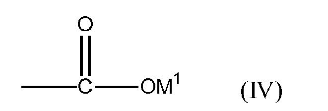
- Examples of such alkylglycosides as described above include are APG™ 325 CS Glycoside® which is described as being a 50% C9-C11 alkyl polyglycoside, also commonly referred to as D-glucopyranoside, (commercially available from Henkel Corp, Ambler Pa.) and Glucopon™ 625 CS which is described as being a 50% C10-C16 alkyl polyglycoside, also commonly referred to as a D-glucopyranoside, (available from Henkel Corp., Ambler Pa.).
- Exemplary alkyl glycosides suitable for use in the practice of this invention include those represented by the formula:

- Examples of such alkylpolyglycoside compounds according to structure V include:
where R is C8 to C10 alkyl chains (Glucopon® 220 UP, Glucopon® 225 DK); where R is C8, C10, C12, C14 and C16 alkyl chains (Glucopon® 425); where R is C12, C14 and C16 alkyl chains (Glucopon® 600 UP, Glucopon® 625 CSUP, and Glucopon® 625 FE, all of which are available from Henkel Corp., Ambler Pa.). Also useful as the alkylpolyglycoside compound is Triton® CG-110 (Union Carbide Corp.). - Another useful alkylglycoside is GLUCOPON 325N which is described as being a C9-C11 alkyl polyglycoside, also commonly referred to as D-glucopyranoside (from Henkel Corp, Ambler Pa.).
- Other suitable alkyl polyglycosides that are commercially available include, but are not limited to, GLUCOPON®, or PLANTAREN® surfactants from Henkel Corporation, Ambler, PA., 19002. Examples of such surfactants include but are not limited to:
- 1. GLUCOPON® 225 Surfactant--an alkyl polyglycoside in which the alkyl group contains 8 to 10 carbon atoms and having an average degree of polymerization of 1.7.
- 2. GLUCOPON® 425 Surfactant--an alkyl polyglycoside in which the alkyl group contains 8 to 16 carbon atoms and having an average degree of polymerization of 1.6.
- 3. GLUCOPON® 625 Surfactant--an alkyl polyglycoside in which the alkyl groups contains 12 to 16 carbon atoms and having an average degree of polymerization of 1.6.
- 4. APG® 325 Surfactant--an alkyl polyglycoside in which the alkyl groups contains 9 to 11 carbon atoms and having an average degree of polymerization of 1.6.
- 5. GLUCOPON® 600 Surfactant--an alkyl polyglycoside in which the alkyl groups contains 12 to 16 carbon atoms and having an average degree of polymerization of 1.4.
- 6. PLANTAREN® 2000 Surfactant--a C8-16 alkyl polyglycoside in which the alkyl group contains 8 to 16 carbon atoms and having an average degree of polymerization of 1.4.
- 7. PLANTAREN® 1300 Surfactant-a C12-16 alkyl polyglycoside in which the alkyl groups contains 12 to 16 carbon atoms and having an average degree of polymerization of 1.6.
- Other suitable polyols include, but are not limited to, alcohol alkoxylates, fatty alcohol alkoxylates, fatty sorbitan esters and their alkoxylates, and the like. Examples of two commercially available surfactants are the ethylene oxide and propylene oxide surfactants Pluronic® and Tetronic® (obtainable from BASF).
- Additional surfactants include, but are not limited to, surfactants having the following general formula:

- Another class of surfactants which may be included in the cleaning compositions is the gemini surfactant. A gemini surfactant (GS) includes two conventional surfactant molecules chemically bonded together by a spacer. Two terminal hydrocarbon tails may be short or long; two polar head groups may be cationic, anionic or nonionic. The spacer may be short or long, flexible or rigid. The GS need not be symmetrically disposed about the center of the spacer. The hydrophilic and hydrophobic groups of each surfactant moiety may be any of those known to be used in conventional surfactants having one hydrophilic group and one hydrophobic group. For example, a typical nonionic gemini surfactant, e.g., a bis-polyoxyethylene alkyl ether, may contain two polyoxyethylene alkyl ether moieties. One type of gemini surfactant which may be included in the cleaning compositions are the nonionic gemini surfactants disclosed in
U.S. 5,945,393 . - Optional antifoam agents also may be used in the cleaning compositions. Such antifoam agents include, but are not limited to, silicon compounds such as siloxanes with glycols, acetylenics and block alkoxy copolymers. Other conventional antifoam agents may be used depending on the specific type of surfactant or combination of surfactants in the cleaning compositions. Workers may use routine experimentation to determine which antifoam agents are suitable for a particular surfactant or combination of surfactants.
- Although both the aqueous acid and aqueous alkaline cleaning compositions may include one or more optional antifoam agents, the aqueous acid cleaning compositions consist essentially of one or more polycarboxylic acid, one or more surfactants and water; and the aqueous alkaline cleaning compositions consist essentially of one or more alkaline compound, one or more surfactants and water. Typically, the surfactant is a nonionic surfactant such as a polyol, such as an alkyl polyglycoside or a nonionic gemini surfactant.
- Optionally, after the aqueous alkaline cleaning step the wafer may be cleaned with a second acid cleaning step. The optional acid cleaning step is a repeat of the first acid cleaning step. The optional acid cleaning step removes any remaining metals which were not removed in the first acid cleaning step and the alkaline cleaning step.
- The following Examples are intended to further illustrate the invention but are not intended to limit the scope of the invention.
- A monocrystalline silicon ingot was bonded to a contact plate and an attachment jig. This was loaded on a conventional wire saw apparatus. The wire saw was coated with abrasive silicon carbide particles. During cutting a slurry containing polyethylene glycol and #600 to #1000 size silicon carbide particles in a weight ratio of 1:1 was sprayed from slurry nozzles of the apparatus onto the ingot. The monocrystalline silicon wafers which were cut from the ingot were then cleaned for 10 minutes at room temperature with a 5wt% aqueous alkaline composition made from a concentrate composed of 0.05wt% Glucopon™ 425N, 6.25wt% sodium carbonate, 17.5wt% sodium hydroxide and 76.2wt% water. Cleaning was done by spraying the wafers with the aqueous alkaline composition using a conventional spraying apparatus.
- After cleaning, the silicon wafers were analyzed for metal contaminants from the cutting process by abstraction with 10% nitric acid mixture at room temperature for 2 minutes and then conventional atomic absorption spectroscopy using a Varian Graphite Furnace AA 2807 Zeeman Atomic Absorption Spectrophotometer. The metal contaminants measured were copper at 1.26 ppb, iron at 1.53 ppb, lead at 0.32 ppb and zinc at 1.77 ppb.
- A monocrystalline silicon ingot was bonded to a contact plate and an attachment jig. This was loaded on a conventional wire saw apparatus. The wire saw was coated with abrasive silicon carbide particles. During cutting a slurry containing polyethylene glycol and #600 to #1000 size silicon carbide particles in a weight ratio of 1:1 was sprayed from slurry nozzles of the apparatus onto the ingot. The monocrystalline silicon wafers which were cut from the ingot were then cleaned for 5 minutes at room temperature with a 5wt% aqueous acid composition made from a concentrate composed of 0.025wt% Glucopon™ 425N, 10wt% oxalic acid and the balance water. The aqueous acid composition was applied to the wafers by a conventional spraying apparatus. Immediately after cleaning with the aqueous acid composition the wafers were spray cleaned with the aqueous alkaline composition used in Example 1. Cleaning with the aqueous alkaline composition was done for 10 minutes.
- After cleaning, the silicon wafers were analyzed for metal contaminants by the same procedure as in Example 1. The metal contaminants measured were copper at 0.22 ppb, iron at 0.6 ppb, lead at 0 ppb and zinc at 0.53 ppb. The aqueous acid composition followed by application of the aqueous alkaline composition removed significantly more metal residues than the aqueous alkaline composition in Example 1.
- A monocrystalline silicon ingot was bonded to a contact plate and an attachment jig. This was loaded on a conventional wire saw apparatus. The wire saw was coated with abrasive silicon carbide particles. During cutting a slurry containing polyethylene glycol and #600 to #1000 size silicon carbide particles in a weight ratio of 1:1 was sprayed from slurry nozzles of the apparatus onto the ingot. The monocrystalline silicon wafers which were cut from the ingot were then cleaned for 5 minutes at room temperature with a 5wt% aqueous acid composition made from a concentrate composed of 0.025wt% Glucopon™ 425N, 10wt% oxalic acid and the balance water. The aqueous acid composition was applied to the wafers by a conventional spraying apparatus. Immediately after cleaning with the aqueous acid composition the wafers were spray cleaned with the aqueous alkaline composition used in Example 1. Cleaning with the aqueous alkaline composition was done for 10 minutes. Immediately after cleaning with the aqueous alkaline composition the wafers were cleaned again for 5 minutes using the aqueous acid composition.
- After cleaning, the silicon wafers were analyzed for metal contaminants from the cutting process as in Example 1. The metal contaminants measured were copper at 0.2 ppb, iron at 0.3 ppb, lead at 0 ppb and zinc at 0.38 ppb. The aqueous acid composition followed by application of the aqueous alkaline composition and then followed by cleaning with the acid cleaner a second time further reduced metal residues.
- A polycrystalline silicon ingot is bonded to a contact plate and an attachment jig. This is loaded on a conventional wire saw apparatus. The wire saw is coated with diamond abrasive particles. During cutting a slurry containing mineral oil and #600 to 1000# size silicon carbide particles in a weight ratio of 1:1 is sprayed from slurry nozzles of the apparatus onto the ingot. The polycrystalline silicon wafers which are cut from the ingot are then cleaned for 5 minutes at room temperature with a 5wt% aqueous acid composition made from a concentrate composed of 0.025wt% Glucopon™ 625, 10wt% citric acid and the balance water. The aqueous acid composition is applied to the wafers by a conventional spraying apparatus at 50° C. Immediately after cleaning with the aqueous acid composition the wafers are spray cleaned with a 5wt% aqueous alkaline composition made from a concentrate containing 0.05wt% Glucopon™ 625, 6wt% sodium carbonate with the balance water. Cleaning with the aqueous alkaline composition is done for 10 minutes.
- After cleaning, the silicon wafers are analyzed as in Example 1 for metal contaminants from the cutting process. The metal contaminants such as copper, iron, lead and zinc are each expected to be in amounts of less than 1 ppb.
Claims (8)
- A method comprising, in sequence, the following:a) applying an aqueous acid composition comprising one or more acids chosen from polycarboxylic acids and inorganic acids to a semiconductor wafer; andb) applying an aqueous alkaline composition comprising one or more alkaline compounds to the semiconductor wafer to remove metals and residue from the material.
- The method of claim 1, further comprising a step of applying a second acid composition comprising one or more acids chosen from polycarboxylic acids and inorganic acids to the semiconductor wafer subsequent to step b.
- The method of claim 1, wherein the aqueous acid composition and the aqueous alkaline composition further comprise one or more surfactants.
- The method of claim 3, wherein the one or more surfactants are nonionic.
- The method of claim 4, wherein the nonionic surfactant is chosen from a polyol and a gemini surfactant.
- The composition of claim 5, wherein the polyol is chosen from a glycoside and a polyglycoside.
- The composition of claim 1, wherein the polycarboxylic acid is chosen from a dicarboxylic acid, a tricarboxylic acid and an oxycarboxylic acid.
- The composition of claim 1 wherein the alkaline compounds are chosen from sodium carbonate, potassium carbonate, sodium bicarbonate, sodium hydroxide, potassium hydroxide and tetra-methyl ammonium hydroxide.
Applications Claiming Priority (1)
| Application Number | Priority Date | Filing Date | Title |
|---|---|---|---|
| US20502009P | 2009-01-14 | 2009-01-14 |
Publications (3)
| Publication Number | Publication Date |
|---|---|
| EP2209134A2 true EP2209134A2 (en) | 2010-07-21 |
| EP2209134A3 EP2209134A3 (en) | 2011-11-02 |
| EP2209134B1 EP2209134B1 (en) | 2017-03-22 |
Family
ID=42101815
Family Applications (1)
| Application Number | Title | Priority Date | Filing Date |
|---|---|---|---|
| EP10150643.4A Not-in-force EP2209134B1 (en) | 2009-01-14 | 2010-01-13 | Method of cleaning semiconductor wafers |
Country Status (6)
| Country | Link |
|---|---|
| US (1) | US8460474B2 (en) |
| EP (1) | EP2209134B1 (en) |
| JP (2) | JP2010226089A (en) |
| KR (2) | KR20100083751A (en) |
| CN (1) | CN101894738B (en) |
| TW (1) | TWI398516B (en) |
Cited By (3)
| Publication number | Priority date | Publication date | Assignee | Title |
|---|---|---|---|---|
| DE102011050903A1 (en) | 2010-09-03 | 2012-03-08 | Schott Solar Ag | Process for the wet-chemical etching of a highly doped semiconductor layer |
| EP2458622A3 (en) * | 2010-11-24 | 2013-05-22 | Air Products and Chemicals, Inc. | Compositions and methods for texturing of silicon wafers |
| KR20140010081A (en) * | 2011-03-21 | 2014-01-23 | 바스프 에스이 | Aqueous, nitrogen-free cleaning composition, preparation and use thereof |
Families Citing this family (16)
| Publication number | Priority date | Publication date | Assignee | Title |
|---|---|---|---|---|
| JP2010226089A (en) * | 2009-01-14 | 2010-10-07 | Rohm & Haas Electronic Materials Llc | Method for cleaning a semiconductor wafer |
| US7955989B2 (en) * | 2009-09-24 | 2011-06-07 | Rohm And Haas Electronic Materials Llc | Texturing semiconductor substrates |
| JP2011124546A (en) | 2009-10-14 | 2011-06-23 | Rohm & Haas Electronic Materials Llc | Method of cleaning and micro-etching semiconductor wafer |
| DE102010056046A1 (en) * | 2010-12-23 | 2012-06-28 | Schott Solar Ag | Method for manufacturing wafer to manufacture e.g. photovoltaic cell that is utilized in solar industry for generation of electric current, involves neutralizing wafer surface with acid, where neutralization takes place by solution |
| CN102554783B (en) * | 2010-12-23 | 2014-12-03 | 中芯国际集成电路制造(上海)有限公司 | Cleaning method of grinding pad |
| CN102115915B (en) * | 2010-12-31 | 2012-08-22 | 百力达太阳能股份有限公司 | Single crystal silicon texture-making additive and single crystal silicon texture-making technology |
| JP6289241B2 (en) * | 2013-06-20 | 2018-03-07 | 東京エレクトロン株式会社 | Liquid processing method, liquid processing apparatus, and storage medium |
| CN105985871A (en) * | 2015-02-10 | 2016-10-05 | 四川迈克生物科技股份有限公司 | Cleaning agent |
| CN107936849B (en) * | 2017-11-10 | 2020-09-15 | 苏州晶瑞化学股份有限公司 | Polishing solution and preparation method and application thereof |
| US10996457B2 (en) | 2018-10-12 | 2021-05-04 | Panasonic Intellectual Property Management Co., Ltd. | Wheel apparatus, light source apparatus, and projection-type image display apparatus |
| US11037792B2 (en) * | 2018-10-25 | 2021-06-15 | Taiwan Semiconductor Manufacturing Company Ltd. | Semiconductor structure etching solution and method for fabricating a semiconductor structure using the same etching solution |
| EP4013194A1 (en) * | 2020-12-11 | 2022-06-15 | Atotech Deutschland GmbH & Co. KG | Aqueous alkaline cleaner solution for glass filler removal and method |
| JP7569677B2 (en) * | 2020-12-17 | 2024-10-18 | 花王株式会社 | Rinse composition for silicon wafers |
| KR102571748B1 (en) | 2021-05-04 | 2023-08-25 | 세메스 주식회사 | Apparatus and method for treating substrate |
| KR20230050771A (en) | 2021-10-08 | 2023-04-17 | 윤채완 | Architectural space market. |
| CN116970446B (en) * | 2023-09-22 | 2024-01-09 | 山东天岳先进科技股份有限公司 | Pretreatment solution, product and application of silicon carbide single crystal material AMB coated copper |
Citations (1)
| Publication number | Priority date | Publication date | Assignee | Title |
|---|---|---|---|---|
| US6568384B1 (en) | 1999-06-08 | 2003-05-27 | Sumitomo Metal Industries, Ltd. | Semiconductor material cutting and processing method |
Family Cites Families (52)
| Publication number | Priority date | Publication date | Assignee | Title |
|---|---|---|---|---|
| US4011389A (en) * | 1975-03-21 | 1977-03-08 | Basf Wyandotte Corporation | Glycoside polyethers |
| US4675125A (en) * | 1984-07-02 | 1987-06-23 | Cincinnati-Vulcan Company | Multi-purpose metal cleaning composition containing a boramide |
| US4581102A (en) * | 1984-08-20 | 1986-04-08 | Olin Corporation | Copper-base alloy cleaning solution |
| US5279677A (en) * | 1991-06-17 | 1994-01-18 | Coral International, Inc. | Rinse aid for metal surfaces |
| DE19525521B4 (en) * | 1994-07-15 | 2007-04-26 | Lam Research Corp.(N.D.Ges.D.Staates Delaware), Fremont | Process for cleaning substrates |
| GB9521837D0 (en) * | 1995-10-25 | 1996-01-03 | Reckitt & Colman Inc | Improved compositions containing organic compounds |
| US5855811A (en) * | 1996-10-03 | 1999-01-05 | Micron Technology, Inc. | Cleaning composition containing tetraalkylammonium salt and use thereof in semiconductor fabrication |
| US5919311A (en) * | 1996-11-15 | 1999-07-06 | Memc Electronic Materials, Inc. | Control of SiO2 etch rate using dilute chemical etchants in the presence of a megasonic field |
| US6204297B1 (en) * | 1996-11-26 | 2001-03-20 | Rhodia Inc. | Nonionic gemini surfactants |
| JPH10209100A (en) * | 1997-01-16 | 1998-08-07 | Mitsubishi Materials Shilicon Corp | Semiconductor substrate cleaning method |
| US8092707B2 (en) * | 1997-04-30 | 2012-01-10 | 3M Innovative Properties Company | Compositions and methods for modifying a surface suited for semiconductor fabrication |
| US6068879A (en) * | 1997-08-26 | 2000-05-30 | Lsi Logic Corporation | Use of corrosion inhibiting compounds to inhibit corrosion of metal plugs in chemical-mechanical polishing |
| EP0928017B1 (en) * | 1997-12-09 | 2014-09-10 | Shin-Etsu Handotai Co., Ltd. | Semiconductor wafer processing method |
| US5837662A (en) * | 1997-12-12 | 1998-11-17 | Memc Electronic Materials, Inc. | Post-lapping cleaning process for silicon wafers |
| US6465403B1 (en) * | 1998-05-18 | 2002-10-15 | David C. Skee | Silicate-containing alkaline compositions for cleaning microelectronic substrates |
| JP2003533865A (en) * | 1998-07-29 | 2003-11-11 | シーエフエムテイ・インコーポレーテツド | Method of wet processing an electronic component using an ozone-containing process fluid in the manufacture of the electronic component |
| US20010052351A1 (en) * | 1998-09-29 | 2001-12-20 | Brian J. Brown | Method for cleaning semiconductor wafer having copper structure formed thereon |
| JP4516176B2 (en) * | 1999-04-20 | 2010-08-04 | 関東化学株式会社 | Substrate cleaning solution for electronic materials |
| DE19953152C1 (en) * | 1999-11-04 | 2001-02-15 | Wacker Siltronic Halbleitermat | Process for wet-chemical treatment of semiconductor wafer after mechanical treatment in lapping machine comprises subjecting to ultrasound in an alkaline cleaning solution before etching and rinsing steps |
| US6709316B1 (en) * | 2000-10-27 | 2004-03-23 | Applied Materials, Inc. | Method and apparatus for two-step barrier layer polishing |
| US7279119B2 (en) * | 2001-06-14 | 2007-10-09 | Ppg Industries Ohio, Inc. | Silica and silica-based slurry |
| US7256167B2 (en) * | 2001-08-31 | 2007-08-14 | Reckitt Benckiser Inc. | Hard surface cleaner comprising suspended particles and oxidizing agent |
| JP2003077875A (en) * | 2001-09-04 | 2003-03-14 | Toshiba Ceramics Co Ltd | Silicon wafer cleaning method |
| JP2003109930A (en) * | 2001-09-28 | 2003-04-11 | Mitsubishi Chemicals Corp | Cleaning solution and method of cleaning board of semiconductor device |
| JP4718762B2 (en) * | 2002-02-19 | 2011-07-06 | 関東化学株式会社 | Semiconductor substrate cleaning liquid composition |
| TWI339680B (en) * | 2002-02-19 | 2011-04-01 | Kanto Kagaku | Washing liquid composition for semiconductor substrate |
| GB2392450A (en) * | 2002-08-31 | 2004-03-03 | Reckitt Benckiser Inc | Liquid detergent compositions |
| US7101456B2 (en) * | 2002-09-20 | 2006-09-05 | Kimberly-Clark Worldwide, Inc. | Ion triggerable, cationic polymers, a method of making same and items using same |
| US6953041B2 (en) * | 2002-10-09 | 2005-10-11 | Micell Technologies, Inc. | Compositions of transition metal species in dense phase carbon dioxide and methods of use thereof |
| KR100634164B1 (en) * | 2003-03-13 | 2006-10-16 | 삼성전자주식회사 | Cleaning solution used in semiconductor manufacturing process |
| JP2005060660A (en) * | 2003-07-31 | 2005-03-10 | Sumitomo Chemical Co Ltd | Cleaning solution for semiconductor substrates |
| US7514363B2 (en) * | 2003-10-23 | 2009-04-07 | Dupont Air Products Nanomaterials Llc | Chemical-mechanical planarization composition having benzenesulfonic acid and per-compound oxidizing agents, and associated method for use |
| EP1717344A4 (en) * | 2004-01-23 | 2008-08-20 | Ebara Corp | PROCESS FOR PROCESSING SUBSTRATE, CATALYTIC PROCESS LIQUID, AND SUBSTRATE PROCESSING APPARATUS |
| US7611588B2 (en) * | 2004-11-30 | 2009-11-03 | Ecolab Inc. | Methods and compositions for removing metal oxides |
| JP4989042B2 (en) | 2005-06-09 | 2012-08-01 | 信越半導体株式会社 | Manufacturing method of substrate for solar cell |
| JP2007150167A (en) * | 2005-11-30 | 2007-06-14 | Shin Etsu Handotai Co Ltd | Semiconductor wafer surface grinding method and manufacturing method |
| DE102006000882A1 (en) * | 2006-01-04 | 2007-07-05 | Henkel Kgaa | Purification of a sawed silicon wafer, useful in microelectronic components and photovoltaics, comprises contacting the silicon wafer with an aqueous, alkaline cleaning solution and a non-ionic surfactant |
| US7456107B2 (en) * | 2006-11-09 | 2008-11-25 | Cabot Microelectronics Corporation | Compositions and methods for CMP of low-k-dielectric materials |
| JP5208409B2 (en) * | 2006-12-15 | 2013-06-12 | 花王株式会社 | Cleaning composition |
| JP2008270584A (en) * | 2007-04-23 | 2008-11-06 | Nippon Chem Ind Co Ltd | Semiconductor wafer polishing composition and polishing method |
| JP5428200B2 (en) * | 2007-05-18 | 2014-02-26 | 三菱化学株式会社 | Semiconductor device substrate cleaning liquid, semiconductor device substrate cleaning method, and semiconductor device substrate manufacturing method |
| TW200940705A (en) * | 2007-10-29 | 2009-10-01 | Ekc Technology Inc | Copper CMP polishing pad cleaning composition comprising of amidoxime compounds |
| US20090107520A1 (en) * | 2007-10-29 | 2009-04-30 | Wai Mun Lee | Amidoxime compounds as chelating agents in semiconductor processes |
| TW200946621A (en) * | 2007-10-29 | 2009-11-16 | Ekc Technology Inc | Chemical mechanical polishing and wafer cleaning composition comprising amidoxime compounds and associated method for use |
| WO2009058275A1 (en) * | 2007-10-29 | 2009-05-07 | Ekc Technology, Inc. | Methods of post chemical mechanical polishing and wafer cleaning using amidoxime compositions |
| US20090120457A1 (en) * | 2007-11-09 | 2009-05-14 | Surface Chemistry Discoveries, Inc. | Compositions and method for removing coatings and preparation of surfaces for use in metal finishing, and manufacturing of electronic and microelectronic devices |
| KR20100082012A (en) * | 2007-11-16 | 2010-07-15 | 이케이씨 테크놀로지, 인코포레이티드 | Compositions for removal of metal hard mask etching residues from a semiconductor substrate |
| DE102007058503B4 (en) * | 2007-12-05 | 2011-08-25 | Siltronic AG, 81737 | Process for the wet-chemical treatment of a semiconductor wafer |
| US8383003B2 (en) * | 2008-06-20 | 2013-02-26 | Nexplanar Corporation | Polishing systems |
| US20100105595A1 (en) * | 2008-10-29 | 2010-04-29 | Wai Mun Lee | Composition comprising chelating agents containing amidoxime compounds |
| JP2010226089A (en) * | 2009-01-14 | 2010-10-07 | Rohm & Haas Electronic Materials Llc | Method for cleaning a semiconductor wafer |
| EP2337089A3 (en) * | 2009-12-17 | 2013-12-11 | Rohm and Haas Electronic Materials LLC | Improved method of texturing semiconductor substrates |
-
2010
- 2010-01-12 JP JP2010004320A patent/JP2010226089A/en active Pending
- 2010-01-13 US US12/657,095 patent/US8460474B2/en not_active Expired - Fee Related
- 2010-01-13 EP EP10150643.4A patent/EP2209134B1/en not_active Not-in-force
- 2010-01-13 TW TW99100769A patent/TWI398516B/en not_active IP Right Cessation
- 2010-01-14 CN CN201010002900.1A patent/CN101894738B/en not_active Expired - Fee Related
- 2010-01-14 KR KR1020100003533A patent/KR20100083751A/en not_active Ceased
-
2015
- 2015-11-02 JP JP2015215582A patent/JP6133380B2/en not_active Expired - Fee Related
-
2016
- 2016-09-19 KR KR1020160119155A patent/KR20160113554A/en not_active Ceased
Patent Citations (1)
| Publication number | Priority date | Publication date | Assignee | Title |
|---|---|---|---|---|
| US6568384B1 (en) | 1999-06-08 | 2003-05-27 | Sumitomo Metal Industries, Ltd. | Semiconductor material cutting and processing method |
Cited By (6)
| Publication number | Priority date | Publication date | Assignee | Title |
|---|---|---|---|---|
| DE102011050903A1 (en) | 2010-09-03 | 2012-03-08 | Schott Solar Ag | Process for the wet-chemical etching of a highly doped semiconductor layer |
| EP2458622A3 (en) * | 2010-11-24 | 2013-05-22 | Air Products and Chemicals, Inc. | Compositions and methods for texturing of silicon wafers |
| KR101362913B1 (en) * | 2010-11-24 | 2014-03-14 | 에어 프로덕츠 앤드 케미칼스, 인코오포레이티드 | Compositions and Methods for Texturing of Silicon Wafers |
| KR20140010081A (en) * | 2011-03-21 | 2014-01-23 | 바스프 에스이 | Aqueous, nitrogen-free cleaning composition, preparation and use thereof |
| EP2688688A4 (en) * | 2011-03-21 | 2014-12-31 | Basf Se | AQUEOUS CLEANING COMPOSITION WITHOUT NITROGEN, PREPARATION AND USE THEREOF |
| US9275851B2 (en) | 2011-03-21 | 2016-03-01 | Basf Se | Aqueous, nitrogen-free cleaning composition and its use for removing residues and contaminants from semiconductor substrates suitable for manufacturing microelectronic devices |
Also Published As
| Publication number | Publication date |
|---|---|
| KR20160113554A (en) | 2016-09-30 |
| KR20100083751A (en) | 2010-07-22 |
| EP2209134B1 (en) | 2017-03-22 |
| CN101894738B (en) | 2014-06-04 |
| JP2016028454A (en) | 2016-02-25 |
| JP6133380B2 (en) | 2017-05-24 |
| EP2209134A3 (en) | 2011-11-02 |
| US20100248494A1 (en) | 2010-09-30 |
| JP2010226089A (en) | 2010-10-07 |
| TWI398516B (en) | 2013-06-11 |
| CN101894738A (en) | 2010-11-24 |
| TW201043690A (en) | 2010-12-16 |
| US8460474B2 (en) | 2013-06-11 |
Similar Documents
| Publication | Publication Date | Title |
|---|---|---|
| EP2209134B1 (en) | Method of cleaning semiconductor wafers | |
| KR101374039B1 (en) | Polishing composition and polishing method | |
| KR101925272B1 (en) | Aqueous, nitrogen-free cleaning composition, preparation and use thereof | |
| JP2008270584A (en) | Semiconductor wafer polishing composition and polishing method | |
| KR101956388B1 (en) | Cleaning solution composition for sapphire wafer | |
| CN114106934B (en) | Sapphire wafer cleaning agent and preparation method thereof | |
| KR20230059813A (en) | Cleaning compositions and methods of use thereof | |
| JP2009040828A (en) | Cleaning composition for wafer or plate | |
| KR102612276B1 (en) | Polishing method and polishing composition set for silicon substrate | |
| KR20060051695A (en) | Oils, slurries and cutting methods for water-soluble cutting | |
| KR101841698B1 (en) | Cleaning solution composition for display window glass | |
| CN112745990B (en) | Non-phosphorus two-component cleaning agent and preparation method and application thereof | |
| KR20080032843A (en) | Glass cleaning composition | |
| CN112745994B (en) | Double-component cleaning agent and preparation method and application thereof | |
| TW201139654A (en) | Composition of cleaning agent for cut object | |
| JP3317839B2 (en) | Detergent composition and method for cleaning sliced wafer or plate | |
| CN114806752B (en) | Single-component cleaning agent with high free alkalinity for monocrystalline large-size silicon wafer | |
| KR20160018470A (en) | Water soluble cutting fluid for fixed abrasive grain wire saw, ingot cutting method using same, and substrate for electronic material obtained by means of same | |
| CN113544248B (en) | Semiconductor wafer cleaning liquid composition and cleaning method using the same | |
| CN110669594B (en) | Silicon carbide single crystal wafer cleaning agent and preparation method and application thereof | |
| CN114350452A (en) | Cleaning agent and preparation method thereof | |
| KR20150017153A (en) | Composition for cleaning of semiconductor wafer | |
| JP2003313584A (en) | Detergent composition | |
| CN114621082B (en) | Ceramic plate cleaning fluid and preparation method and application thereof | |
| KR20130046293A (en) | Composition of cleaning wafer for solar cell |
Legal Events
| Date | Code | Title | Description |
|---|---|---|---|
| PUAI | Public reference made under article 153(3) epc to a published international application that has entered the european phase |
Free format text: ORIGINAL CODE: 0009012 |
|
| 17P | Request for examination filed |
Effective date: 20100113 |
|
| AK | Designated contracting states |
Kind code of ref document: A2 Designated state(s): AT BE BG CH CY CZ DE DK EE ES FI FR GB GR HR HU IE IS IT LI LT LU LV MC MK MT NL NO PL PT RO SE SI SK SM TR |
|
| AX | Request for extension of the european patent |
Extension state: AL BA RS |
|
| PUAL | Search report despatched |
Free format text: ORIGINAL CODE: 0009013 |
|
| AK | Designated contracting states |
Kind code of ref document: A3 Designated state(s): AT BE BG CH CY CZ DE DK EE ES FI FR GB GR HR HU IE IS IT LI LT LU LV MC MK MT NL NO PL PT RO SE SI SK SM TR |
|
| AX | Request for extension of the european patent |
Extension state: AL BA RS |
|
| RIC1 | Information provided on ipc code assigned before grant |
Ipc: H01L 31/18 20060101ALI20110927BHEP Ipc: H01L 21/02 20060101AFI20110927BHEP |
|
| 17Q | First examination report despatched |
Effective date: 20111028 |
|
| REG | Reference to a national code |
Ref country code: DE Ref legal event code: R079 Ref document number: 602010040883 Country of ref document: DE Free format text: PREVIOUS MAIN CLASS: H01L0021020000 Ipc: H01L0021306000 |
|
| GRAP | Despatch of communication of intention to grant a patent |
Free format text: ORIGINAL CODE: EPIDOSNIGR1 |
|
| INTG | Intention to grant announced |
Effective date: 20160309 |
|
| RIC1 | Information provided on ipc code assigned before grant |
Ipc: H01L 31/02 20060101ALI20160226BHEP Ipc: H01L 21/306 20060101AFI20160226BHEP |
|
| GRAJ | Information related to disapproval of communication of intention to grant by the applicant or resumption of examination proceedings by the epo deleted |
Free format text: ORIGINAL CODE: EPIDOSDIGR1 |
|
| INTC | Intention to grant announced (deleted) | ||
| RAP1 | Party data changed (applicant data changed or rights of an application transferred) |
Owner name: SUN CHEMICAL CORPORATION |
|
| GRAP | Despatch of communication of intention to grant a patent |
Free format text: ORIGINAL CODE: EPIDOSNIGR1 |
|
| INTG | Intention to grant announced |
Effective date: 20160930 |
|
| GRAS | Grant fee paid |
Free format text: ORIGINAL CODE: EPIDOSNIGR3 |
|
| GRAA | (expected) grant |
Free format text: ORIGINAL CODE: 0009210 |
|
| AK | Designated contracting states |
Kind code of ref document: B1 Designated state(s): AT BE BG CH CY CZ DE DK EE ES FI FR GB GR HR HU IE IS IT LI LT LU LV MC MK MT NL NO PL PT RO SE SI SK SM TR |
|
| REG | Reference to a national code |
Ref country code: GB Ref legal event code: FG4D |
|
| REG | Reference to a national code |
Ref country code: CH Ref legal event code: EP |
|
| REG | Reference to a national code |
Ref country code: AT Ref legal event code: REF Ref document number: 878528 Country of ref document: AT Kind code of ref document: T Effective date: 20170415 |
|
| REG | Reference to a national code |
Ref country code: IE Ref legal event code: FG4D |
|
| REG | Reference to a national code |
Ref country code: DE Ref legal event code: R096 Ref document number: 602010040883 Country of ref document: DE |
|
| REG | Reference to a national code |
Ref country code: NL Ref legal event code: MP Effective date: 20170322 |
|
| PG25 | Lapsed in a contracting state [announced via postgrant information from national office to epo] |
Ref country code: GR Free format text: LAPSE BECAUSE OF FAILURE TO SUBMIT A TRANSLATION OF THE DESCRIPTION OR TO PAY THE FEE WITHIN THE PRESCRIBED TIME-LIMIT Effective date: 20170623 Ref country code: FI Free format text: LAPSE BECAUSE OF FAILURE TO SUBMIT A TRANSLATION OF THE DESCRIPTION OR TO PAY THE FEE WITHIN THE PRESCRIBED TIME-LIMIT Effective date: 20170322 Ref country code: NO Free format text: LAPSE BECAUSE OF FAILURE TO SUBMIT A TRANSLATION OF THE DESCRIPTION OR TO PAY THE FEE WITHIN THE PRESCRIBED TIME-LIMIT Effective date: 20170622 Ref country code: HR Free format text: LAPSE BECAUSE OF FAILURE TO SUBMIT A TRANSLATION OF THE DESCRIPTION OR TO PAY THE FEE WITHIN THE PRESCRIBED TIME-LIMIT Effective date: 20170322 Ref country code: LT Free format text: LAPSE BECAUSE OF FAILURE TO SUBMIT A TRANSLATION OF THE DESCRIPTION OR TO PAY THE FEE WITHIN THE PRESCRIBED TIME-LIMIT Effective date: 20170322 |
|
| REG | Reference to a national code |
Ref country code: LT Ref legal event code: MG4D |
|
| REG | Reference to a national code |
Ref country code: AT Ref legal event code: MK05 Ref document number: 878528 Country of ref document: AT Kind code of ref document: T Effective date: 20170322 |
|
| PG25 | Lapsed in a contracting state [announced via postgrant information from national office to epo] |
Ref country code: SE Free format text: LAPSE BECAUSE OF FAILURE TO SUBMIT A TRANSLATION OF THE DESCRIPTION OR TO PAY THE FEE WITHIN THE PRESCRIBED TIME-LIMIT Effective date: 20170322 Ref country code: BG Free format text: LAPSE BECAUSE OF FAILURE TO SUBMIT A TRANSLATION OF THE DESCRIPTION OR TO PAY THE FEE WITHIN THE PRESCRIBED TIME-LIMIT Effective date: 20170622 Ref country code: LV Free format text: LAPSE BECAUSE OF FAILURE TO SUBMIT A TRANSLATION OF THE DESCRIPTION OR TO PAY THE FEE WITHIN THE PRESCRIBED TIME-LIMIT Effective date: 20170322 |
|
| PG25 | Lapsed in a contracting state [announced via postgrant information from national office to epo] |
Ref country code: NL Free format text: LAPSE BECAUSE OF FAILURE TO SUBMIT A TRANSLATION OF THE DESCRIPTION OR TO PAY THE FEE WITHIN THE PRESCRIBED TIME-LIMIT Effective date: 20170322 |
|
| PG25 | Lapsed in a contracting state [announced via postgrant information from national office to epo] |
Ref country code: ES Free format text: LAPSE BECAUSE OF FAILURE TO SUBMIT A TRANSLATION OF THE DESCRIPTION OR TO PAY THE FEE WITHIN THE PRESCRIBED TIME-LIMIT Effective date: 20170322 Ref country code: RO Free format text: LAPSE BECAUSE OF FAILURE TO SUBMIT A TRANSLATION OF THE DESCRIPTION OR TO PAY THE FEE WITHIN THE PRESCRIBED TIME-LIMIT Effective date: 20170322 Ref country code: SK Free format text: LAPSE BECAUSE OF FAILURE TO SUBMIT A TRANSLATION OF THE DESCRIPTION OR TO PAY THE FEE WITHIN THE PRESCRIBED TIME-LIMIT Effective date: 20170322 Ref country code: EE Free format text: LAPSE BECAUSE OF FAILURE TO SUBMIT A TRANSLATION OF THE DESCRIPTION OR TO PAY THE FEE WITHIN THE PRESCRIBED TIME-LIMIT Effective date: 20170322 Ref country code: AT Free format text: LAPSE BECAUSE OF FAILURE TO SUBMIT A TRANSLATION OF THE DESCRIPTION OR TO PAY THE FEE WITHIN THE PRESCRIBED TIME-LIMIT Effective date: 20170322 Ref country code: CZ Free format text: LAPSE BECAUSE OF FAILURE TO SUBMIT A TRANSLATION OF THE DESCRIPTION OR TO PAY THE FEE WITHIN THE PRESCRIBED TIME-LIMIT Effective date: 20170322 |
|
| PG25 | Lapsed in a contracting state [announced via postgrant information from national office to epo] |
Ref country code: PT Free format text: LAPSE BECAUSE OF FAILURE TO SUBMIT A TRANSLATION OF THE DESCRIPTION OR TO PAY THE FEE WITHIN THE PRESCRIBED TIME-LIMIT Effective date: 20170724 Ref country code: IS Free format text: LAPSE BECAUSE OF FAILURE TO SUBMIT A TRANSLATION OF THE DESCRIPTION OR TO PAY THE FEE WITHIN THE PRESCRIBED TIME-LIMIT Effective date: 20170722 Ref country code: SM Free format text: LAPSE BECAUSE OF FAILURE TO SUBMIT A TRANSLATION OF THE DESCRIPTION OR TO PAY THE FEE WITHIN THE PRESCRIBED TIME-LIMIT Effective date: 20170322 Ref country code: PL Free format text: LAPSE BECAUSE OF FAILURE TO SUBMIT A TRANSLATION OF THE DESCRIPTION OR TO PAY THE FEE WITHIN THE PRESCRIBED TIME-LIMIT Effective date: 20170322 |
|
| REG | Reference to a national code |
Ref country code: DE Ref legal event code: R097 Ref document number: 602010040883 Country of ref document: DE |
|
| REG | Reference to a national code |
Ref country code: FR Ref legal event code: PLFP Year of fee payment: 9 |
|
| PLBE | No opposition filed within time limit |
Free format text: ORIGINAL CODE: 0009261 |
|
| STAA | Information on the status of an ep patent application or granted ep patent |
Free format text: STATUS: NO OPPOSITION FILED WITHIN TIME LIMIT |
|
| PG25 | Lapsed in a contracting state [announced via postgrant information from national office to epo] |
Ref country code: DK Free format text: LAPSE BECAUSE OF FAILURE TO SUBMIT A TRANSLATION OF THE DESCRIPTION OR TO PAY THE FEE WITHIN THE PRESCRIBED TIME-LIMIT Effective date: 20170322 |
|
| 26N | No opposition filed |
Effective date: 20180102 |
|
| PG25 | Lapsed in a contracting state [announced via postgrant information from national office to epo] |
Ref country code: IT Free format text: LAPSE BECAUSE OF FAILURE TO SUBMIT A TRANSLATION OF THE DESCRIPTION OR TO PAY THE FEE WITHIN THE PRESCRIBED TIME-LIMIT Effective date: 20170322 Ref country code: SI Free format text: LAPSE BECAUSE OF FAILURE TO SUBMIT A TRANSLATION OF THE DESCRIPTION OR TO PAY THE FEE WITHIN THE PRESCRIBED TIME-LIMIT Effective date: 20170322 |
|
| PGFP | Annual fee paid to national office [announced via postgrant information from national office to epo] |
Ref country code: DE Payment date: 20180129 Year of fee payment: 9 Ref country code: GB Payment date: 20180129 Year of fee payment: 9 |
|
| PGFP | Annual fee paid to national office [announced via postgrant information from national office to epo] |
Ref country code: FR Payment date: 20180125 Year of fee payment: 9 |
|
| REG | Reference to a national code |
Ref country code: CH Ref legal event code: PL |
|
| PG25 | Lapsed in a contracting state [announced via postgrant information from national office to epo] |
Ref country code: LU Free format text: LAPSE BECAUSE OF NON-PAYMENT OF DUE FEES Effective date: 20180113 |
|
| REG | Reference to a national code |
Ref country code: IE Ref legal event code: MM4A |
|
| REG | Reference to a national code |
Ref country code: BE Ref legal event code: MM Effective date: 20180131 |
|
| PG25 | Lapsed in a contracting state [announced via postgrant information from national office to epo] |
Ref country code: LI Free format text: LAPSE BECAUSE OF NON-PAYMENT OF DUE FEES Effective date: 20180131 Ref country code: CH Free format text: LAPSE BECAUSE OF NON-PAYMENT OF DUE FEES Effective date: 20180131 Ref country code: BE Free format text: LAPSE BECAUSE OF NON-PAYMENT OF DUE FEES Effective date: 20180131 |
|
| PG25 | Lapsed in a contracting state [announced via postgrant information from national office to epo] |
Ref country code: IE Free format text: LAPSE BECAUSE OF NON-PAYMENT OF DUE FEES Effective date: 20180113 |
|
| PG25 | Lapsed in a contracting state [announced via postgrant information from national office to epo] |
Ref country code: MC Free format text: LAPSE BECAUSE OF FAILURE TO SUBMIT A TRANSLATION OF THE DESCRIPTION OR TO PAY THE FEE WITHIN THE PRESCRIBED TIME-LIMIT Effective date: 20170322 |
|
| REG | Reference to a national code |
Ref country code: DE Ref legal event code: R119 Ref document number: 602010040883 Country of ref document: DE |
|
| GBPC | Gb: european patent ceased through non-payment of renewal fee |
Effective date: 20190113 |
|
| PG25 | Lapsed in a contracting state [announced via postgrant information from national office to epo] |
Ref country code: DE Free format text: LAPSE BECAUSE OF NON-PAYMENT OF DUE FEES Effective date: 20190801 Ref country code: FR Free format text: LAPSE BECAUSE OF NON-PAYMENT OF DUE FEES Effective date: 20190131 |
|
| PG25 | Lapsed in a contracting state [announced via postgrant information from national office to epo] |
Ref country code: GB Free format text: LAPSE BECAUSE OF NON-PAYMENT OF DUE FEES Effective date: 20190113 |
|
| PG25 | Lapsed in a contracting state [announced via postgrant information from national office to epo] |
Ref country code: MT Free format text: LAPSE BECAUSE OF NON-PAYMENT OF DUE FEES Effective date: 20180113 |
|
| PG25 | Lapsed in a contracting state [announced via postgrant information from national office to epo] |
Ref country code: TR Free format text: LAPSE BECAUSE OF FAILURE TO SUBMIT A TRANSLATION OF THE DESCRIPTION OR TO PAY THE FEE WITHIN THE PRESCRIBED TIME-LIMIT Effective date: 20170322 |
|
| PG25 | Lapsed in a contracting state [announced via postgrant information from national office to epo] |
Ref country code: HU Free format text: LAPSE BECAUSE OF FAILURE TO SUBMIT A TRANSLATION OF THE DESCRIPTION OR TO PAY THE FEE WITHIN THE PRESCRIBED TIME-LIMIT; INVALID AB INITIO Effective date: 20100113 |
|
| PG25 | Lapsed in a contracting state [announced via postgrant information from national office to epo] |
Ref country code: MK Free format text: LAPSE BECAUSE OF NON-PAYMENT OF DUE FEES Effective date: 20170322 Ref country code: CY Free format text: LAPSE BECAUSE OF FAILURE TO SUBMIT A TRANSLATION OF THE DESCRIPTION OR TO PAY THE FEE WITHIN THE PRESCRIBED TIME-LIMIT Effective date: 20170322 |