EP2208778A1 - Procédé et dispositif destinés au traitement électrique d'espaces de réaction - Google Patents
Procédé et dispositif destinés au traitement électrique d'espaces de réaction Download PDFInfo
- Publication number
- EP2208778A1 EP2208778A1 EP09000698A EP09000698A EP2208778A1 EP 2208778 A1 EP2208778 A1 EP 2208778A1 EP 09000698 A EP09000698 A EP 09000698A EP 09000698 A EP09000698 A EP 09000698A EP 2208778 A1 EP2208778 A1 EP 2208778A1
- Authority
- EP
- European Patent Office
- Prior art keywords
- charge storage
- storage devices
- voltage
- discharging
- partially
- Prior art date
- Legal status (The legal status is an assumption and is not a legal conclusion. Google has not performed a legal analysis and makes no representation as to the accuracy of the status listed.)
- Withdrawn
Links
Images


Classifications
-
- C—CHEMISTRY; METALLURGY
- C12—BIOCHEMISTRY; BEER; SPIRITS; WINE; VINEGAR; MICROBIOLOGY; ENZYMOLOGY; MUTATION OR GENETIC ENGINEERING
- C12M—APPARATUS FOR ENZYMOLOGY OR MICROBIOLOGY; APPARATUS FOR CULTURING MICROORGANISMS FOR PRODUCING BIOMASS, FOR GROWING CELLS OR FOR OBTAINING FERMENTATION OR METABOLIC PRODUCTS, i.e. BIOREACTORS OR FERMENTERS
- C12M35/00—Means for application of stress for stimulating the growth of microorganisms or the generation of fermentation or metabolic products; Means for electroporation or cell fusion
- C12M35/02—Electrical or electromagnetic means, e.g. for electroporation or for cell fusion
-
- C—CHEMISTRY; METALLURGY
- C12—BIOCHEMISTRY; BEER; SPIRITS; WINE; VINEGAR; MICROBIOLOGY; ENZYMOLOGY; MUTATION OR GENETIC ENGINEERING
- C12M—APPARATUS FOR ENZYMOLOGY OR MICROBIOLOGY; APPARATUS FOR CULTURING MICROORGANISMS FOR PRODUCING BIOMASS, FOR GROWING CELLS OR FOR OBTAINING FERMENTATION OR METABOLIC PRODUCTS, i.e. BIOREACTORS OR FERMENTERS
- C12M1/00—Apparatus for enzymology or microbiology
- C12M1/42—Apparatus for the treatment of microorganisms or enzymes with electrical or wave energy, e.g. magnetism, sonic waves
-
- C—CHEMISTRY; METALLURGY
- C12—BIOCHEMISTRY; BEER; SPIRITS; WINE; VINEGAR; MICROBIOLOGY; ENZYMOLOGY; MUTATION OR GENETIC ENGINEERING
- C12M—APPARATUS FOR ENZYMOLOGY OR MICROBIOLOGY; APPARATUS FOR CULTURING MICROORGANISMS FOR PRODUCING BIOMASS, FOR GROWING CELLS OR FOR OBTAINING FERMENTATION OR METABOLIC PRODUCTS, i.e. BIOREACTORS OR FERMENTERS
- C12M1/00—Apparatus for enzymology or microbiology
- C12M1/16—Apparatus for enzymology or microbiology containing, or adapted to contain, solid media
- C12M1/18—Multiple fields or compartments
-
- C—CHEMISTRY; METALLURGY
- C12—BIOCHEMISTRY; BEER; SPIRITS; WINE; VINEGAR; MICROBIOLOGY; ENZYMOLOGY; MUTATION OR GENETIC ENGINEERING
- C12M—APPARATUS FOR ENZYMOLOGY OR MICROBIOLOGY; APPARATUS FOR CULTURING MICROORGANISMS FOR PRODUCING BIOMASS, FOR GROWING CELLS OR FOR OBTAINING FERMENTATION OR METABOLIC PRODUCTS, i.e. BIOREACTORS OR FERMENTERS
- C12M3/00—Tissue, human, animal or plant cell, or virus culture apparatus
- C12M3/006—Cell injection or fusion devices
-
- C—CHEMISTRY; METALLURGY
- C12—BIOCHEMISTRY; BEER; SPIRITS; WINE; VINEGAR; MICROBIOLOGY; ENZYMOLOGY; MUTATION OR GENETIC ENGINEERING
- C12N—MICROORGANISMS OR ENZYMES; COMPOSITIONS THEREOF; PROPAGATING, PRESERVING, OR MAINTAINING MICROORGANISMS; MUTATION OR GENETIC ENGINEERING; CULTURE MEDIA
- C12N15/00—Mutation or genetic engineering; DNA or RNA concerning genetic engineering, vectors, e.g. plasmids, or their isolation, preparation or purification; Use of hosts therefor
- C12N15/09—Recombinant DNA-technology
- C12N15/87—Introduction of foreign genetic material using processes not otherwise provided for, e.g. co-transformation
Definitions
- the invention relates to a method for applying at least one reaction space with at least one electrical voltage pulse by discharging at least one charge storage device for storing electrical charges.
- the invention further relates to a device for applying at least one reaction space having at least one voltage pulse, which comprises at least two electrical charge storage devices for storing electrical charges and at least one voltage supply device for charging the charge storage devices and / or at least one discharge device for partially discharging the charge storage devices.
- a preferred method for introducing foreign molecules into the cells is electroporation, which in contrast to chemical methods is not dependent on the simultaneous transport of other biologically active molecules.
- electroporation the foreign molecules are introduced from a buffer solution adapted to the cells or a cell culture medium by a brief current flow into the cells, whereby the cell membrane is made permeable to the foreign molecules by the action of electrical voltage pulses or the resulting electric field and current flow.
- the cell suspension is often located in a so-called cuvette, ie a narrow, open vessel whose sample space has two opposite, parallel electrodes in the side walls, which serve to apply the electrical voltage.
- the biologically active molecules first enter the cytoplasm, where they may already be able to perform their function, and then, under certain conditions, into the nucleus.
- a strong electric field ie a short voltage pulse with high current density
- cells, cell derivatives, subcellular particles and / or vesicles can be fused in addition.
- electrofusion for example, the cells are first brought into close membrane contact by an inhomogeneous alternating electric field. The subsequent application of an electric field pulse then leads to the interaction of membrane parts, which ultimately leads to fusion.
- comparable apparatus devices can be used, as for electroporation.
- living cells can also be stimulated by electric fields in a manner that alters their characteristics.
- Multi-reaction vessels for electroporation, electrofusion, or electrostimulation of living cells are used primarily in biochemical and pharmaceutical applications when a variety of reaction approaches occur simultaneously must be tested.
- Such containers are generally referred to as multi-well plates, microtiter plates or multi-wells.
- the containers usually consist of a plurality of reaction spaces, each having two electrodes which are in contact with the reaction mixture, for example a cell suspension, in the reaction space.
- the two electrodes of a reaction space generate an electrical field when an electrical voltage is applied in the interior of the reaction space.
- an electric current is generated by the surrounding electrodes of different polarity in addition to the electric field.
- the electrodes of the same polarity, ie, for example, all cathodes and / or all anodes, different reaction chambers are either integrally formed or electrically coupled together so that they can be connected via a common electrical contact with the voltage source.
- a problem with the electrical treatment of such microtiter plates is that the time required for the single reaction spaces to be charged with one or more voltage pulses is very long. This is due to the fact that a great many voltage pulses have to be delivered in succession, particularly in the case of individual processing of the reaction vessels, which places very high demands on the capacities and charge times of the charge storage devices or capacitors used, especially at high voltage values and / or energies of the electrical pulses.
- the US-A-6,150,148 a method and a device for electroporation, wherein a plurality of voltage pulses are generated for the admission of a reaction space.
- the device has a voltage source, by means of which two capacitors can be charged via a voltage divider and in each case one transistor.
- the capacitors are discharged via controllable switches, so that the reaction space can be subjected to several successive voltage pulses, for example at least one voltage pulse with a relatively high voltage amplitude and at least one voltage pulse with a smaller voltage amplitude.
- this known device has the disadvantage that the two capacitors must be recharged after each treatment of a reaction space, or at least after the treatment of fewer reaction spaces, so that pauses arise again and again Extend process time in total.
- the object of the invention is to provide a method and a device with which reaction spaces can be acted upon within the shortest possible time by one or more voltage pulses.
- the method according to the invention enables very fast voltage pulse sequences, be it in applications with multiple pulses or in applications in which a plurality of reaction spaces must be applied successively and / or simultaneously with voltage pulses. In particular, in high-throughput process, thereby the process time can be significantly reduced.
- At least partial discharging in the sense of the invention means that the respective charge storage device does not have to be completely discharged when a voltage pulse is delivered, but merely outputs the voltage difference which is required for the voltage pulse. It can therefore remain after discharging a residual voltage in the charge storage device.
- At least partially synchronously in the sense of the invention means that the charging or discharging processes take place at least partially synchronously, ie. H. both processes can take place either synchronously or at different times, in the latter case one process still running or already running while the other process has already ended or has not yet begun.
- the at least partial discharge may be a very short time event in delivering a voltage pulse, the charge storage device in question will be charged during the "simultaneous" charge or partial discharge prior to and / or after the end of the Discharge inactive until the prolonged charging or partial unloading process is completed.
- “Loading or partial unloading” in the sense of the invention means that the charge storage device is placed in readiness for the next or to deliver the following voltage pulse. That is, the voltage level in the charge storage device is adjusted to the voltage required for the next voltage pulse. This can be done on the one hand by charging the charge storage device to the voltage required for the next voltage pulse or on the other hand by partial discharge to the voltage provided for the next voltage pulse.
- the voltage level in the charge storage device is adapted to the new, lower voltage level for the next reaction space by partial discharge by means of a discharge device, for example via an electrical load, preferably by means of a discharge resistor.
- the inventive method is repeated several times, d. H. several cycles of the process steps are run through, so that, for example, a large number of reaction spaces can be treated electrically one after the other, the process only being ended when all the reaction spaces to be treated have been subjected to at least one voltage pulse.
- the method according to the invention can therefore be used without problems in high-throughput processes using multiwell plates, preferably 96-well or 384-well plates.
- the method according to the invention can be used to charge a single reaction space or a cuvette with a plurality of voltage pulses or the electrical treatment of a plurality of reaction spaces.
- successive many reaction chambers can be acted upon in a short time with voltage pulses, wherein always at least two reaction chambers can be treated simultaneously.
- at least two reaction chambers can be acted upon simultaneously with voltage pulses, so that the speed of the treatment of a plurality of reaction chambers increases significantly.
- This inventive solution is particularly advantageous when voltage pulses are to be generated, which consist of a short voltage pulse with a relatively high voltage amplitude and / or relatively low energy and a longer voltage pulse with a lower voltage amplitude and / or higher energy. If several reaction chambers are to be subjected to such double voltage pulses in succession in a relatively short time, for example when using multiwell plates in the high-throughput process, the distances between the application of the individual reaction spaces when using a single capacitor for the longer voltage pulse would be relatively long, since the capacitor after the discharge should be adjusted again by charging or partial discharge to the voltage specified for the next voltage pulse voltage and this larger amounts of electrical energy are applied.
- one of the two charge storage devices is always discharged, while the other charge storage device is charged or partially discharged, so that very many reaction spaces can be subjected to voltage pulses within a short time.
- Charging or partially discharging the first charge storage device with a lower energy requirement is not a time-limiting factor since the first charge storage device, e.g. during the prolonged discharge of one of the two second charge storage devices, recharged or partially discharged.
- At the beginning of the method according to the invention at least two first charge storage devices are preferably initially charged simultaneously or one after the other. After completion of the charging processes, these two first charge storage devices are then discharged, wherein at least two reaction spaces are each subjected to a voltage pulse, preferably a short voltage pulse with a relatively high voltage amplitude. These two reaction spaces are then each acted upon by a further voltage pulse after a short break or without interruption, preferably a longer voltage pulse with a lower voltage amplitude, these voltage pulses being generated by the at least partial discharge of the second charge storage devices.
- At least two further second charge storage devices as well as the first two charge storage devices are charged or partially discharged, so that the entire process duration is not prolonged by the charging or discharging processes and the corresponding charge storage devices are immediately available again when the next reaction space needs to be treated.
- the same or two further reaction spaces can then each be subjected to a voltage pulse.
- the previously charged or partially discharged second charge storage devices are then at least partially discharged again, while temporally parallel the previously discharged charge storage devices are recharged or partially discharged.
- the loading and unloading operations described above can be repeated as often as desired so that a large number of voltage pulses can be delivered in a relatively short time. In this way, a plurality of reaction chambers in a relatively short time with voltage pulses, in particular double pulses, are applied.
- all charge storage devices can be charged at the beginning of the process before step a), so that all charge storage devices can be discharged if necessary.
- the respective charge storage device can also be charged shortly before discharging.
- At least two charge storage devices form a storage module, wherein one of the charge storage devices in the application is at least partially discharged or ready for discharge, while the other charge storage device is charged or partially discharged, so that the storage module as a whole at any time the voltage required for the next voltage pulse can be stored and at least partially discharged.
- the loading and unloading operations can be carried out either synchronously or at different times.
- the first charge storage devices have a capacity of at least 10 ⁇ F, preferably at least 50 ⁇ F, in particular at least 100 ⁇ F, and / or with an initial voltage of 10 to 1500 V, preferably 20 to 1200 V, in particular 50 to 1000 V, are discharged at a pulse duration of 2 ⁇ s to 40 ms, preferably 5 ⁇ s to 20 ms, in particular 10 ⁇ s to 10 ms.
- the second charge storage devices have a capacity of at least 100 uF, preferably at least 500 uF, in particular at least 1000 uF, and / or with an initial voltage of 10 to 240 V, preferably 20 to 200 V, in particular 50 to 150 V, at a pulse duration of 1 ms to 500 ms, preferably 2 ms to 350 ms, in particular 4 ms to 250 ms discharged.
- steps c) and d) or steps b) to e) at least 6, 8, 16, 24, 32, 48, 64, 96, 128 , 192, 256, 384, 1536, 3456 or 6144 times.
- containers which comprise a plurality of reaction spaces, preferably 6, 8, 16, 24, 32, 48, 64, 96, 128, 192, 256, 384, 1536, 3456 or 6144, can be acted upon in succession with at least one voltage pulse in succession ,
- reaction spaces are acted upon in succession, which are spatially as far away from each other, as in this way negative effects can be better distributed by the heat generated by the voltage pulses.
- the discharging of the charge storage devices is controlled in such a way that at least two reaction spaces are successively charged with voltage pulses of different voltages, in which the voltage remaining after the first reaction space is charged in the respective charge storage device is the voltage of the voltage pulse to be subsequently delivered comes as close as possible.
- the should in the respective charge storage device remaining voltage ideally be slightly smaller, slightly larger or approximately equal to the voltage of the subsequently to be delivered voltage pulse.
- a so-called Ladungshubminimierung should be done, ie that a reaction space is selected for the next voltage pulse to be applied to a voltage amplitude which comes closest to the voltage remaining in the charge storage device voltage, regardless of whether the following voltage slightly higher or a little lower.
- the charge or discharge required between the two voltage pulses should be minimized.
- it is pulsed in ascending order, ie the voltage of the first voltage pulse is less than the voltage of the following voltage pulse.
- discharging between the voltage pulses can be avoided. Due to the sequential processing of voltage pulses, the process duration can advantageously be additionally reduced.
- the invention also relates to a method for applying at least two reaction spaces each having at least one electrical voltage pulse by discharging at least one charge storage device for storing electrical charges, in which the discharging of the charge storage device is controlled such that voltage pulses of different voltages are applied successively to at least two reaction spaces, in which the voltage remaining in the charge storage device after the application of the first reaction space comes as close as possible to the voltage of the voltage pulse to be subsequently delivered.
- the process duration can advantageously be significantly reduced since no time is required for charging or discharging between two voltage pulses or this time is at least significantly reduced.
- the voltage remaining in the respective charge storage device is preferably slightly smaller, slightly larger or approximately equal to the voltage of the voltage pulse to be subsequently delivered.
- the charge or discharge required between the two voltage pulses should be minimized.
- the voltage of the first voltage pulse is less than the voltage of the following voltage pulse.
- the charge storage device for. B. the feeding capacitor bank, emits energy pulses, reduces the voltage in the charge storage.
- the charge storage device For the next reaction space, the charge storage device must now be recharged to the voltage required for the next reaction space before the pulses. If the voltage pulses within a contacting section are sorted, for example, according to a decreasing initial voltage, then the charging and discharging voltage swing can be minimized and thus the efficiency can be increased.
- the sequence in which the reaction spaces are processed within a contacting section can be selected in temperature-sensitive experiments such that the adjacent reaction spaces within a container are pulsed with as large a time interval as possible in order to increase the temperature rise of a reaction space next to a just pulsed reaction space as quickly as possible decay again before this reaction space is subjected to a voltage pulse.
- the object is further achieved by a device in which at least two of the charge storage devices form a common storage module which can be discharged at any time, so that these charge storage devices form a unit that always discharges as required after a first charging process can be done without a time-consuming loading or unloading must be performed in between.
- the at least two charge storage devices are preferably electrically coupled via a common interface to a pulse generation unit, a switching unit and / or a distribution device for electrical voltage pulses.
- Electrically coupled in the sense of the invention means that two components or components of the electrical circuit arrangement directly, d. H. without intermediate components, or indirectly, d. H. with components connected between the components, are electrically connected together.
- At least one further charge storage device may be provided, which is preferably electrically coupled via at least one further interface to the pulse generation unit, the switching unit and / or the distribution device for electrical voltage pulses. In this way, it is possible either to treat at least two reaction spaces simultaneously or to generate double pulses, which are applied to at least one reaction space.
- the at least one further charge storage device is electrically coupled to a voltage supply device and that at least the at least two charge storage devices are electrically coupled to a common voltage supply device.
- This embodiment is particularly advantageous when voltage pulses are to be generated, which consist of a short voltage pulse with a relatively high voltage amplitude and a longer voltage pulse with a lower voltage amplitude.
- the charge storage device can generate a short voltage pulse, while the memory module composed of two charge storage devices provides a longer voltage pulse. Consequently, in the device according to the invention, one can always the two charge storage devices of a memory module are discharged while the other charge storage device of the memory module is charged, so that a large number of reaction chambers can be applied within a short time with voltage pulses.
- the charging of the individual charge storage devices is not a time-limiting factor, since this charge storage device can be charged during the longer-lasting discharge of the memory module. Even in the event that the power supply unit (power supply) should not be strong and fast enough, the time required for the charging process can be minimized by the inventive method.
- At least four charge storage devices can also be provided, which together form at least two storage modules.
- a memory module via a single or common interface with the pulse generation unit, the switching unit and / or the distribution device for electrical voltage pulses is electrically coupled.
- the device according to the invention can always act on two reaction spaces simultaneously, each with one voltage pulse. Since no time is required for the charging of a single capacitor between two successive voltage pulses, consequently very many reaction spaces can be subjected to voltage pulses in a relatively short time by means of the device according to the invention.
- the device according to the invention is therefore particularly suitable for use in high-throughput processes in which a large number of reaction spaces have to be subjected to at least one voltage pulse in a short time.
- At least two voltage supply devices can be provided, each voltage supply device being electrically coupled to one respective storage module.
- At least four voltage supply devices and at least six charge storage devices may also be provided.
- This embodiment of the device according to the invention can be used particularly advantageously in high-throughput processes in which many reaction spaces have to be subjected to double voltage pulses in a short time.
- two reaction chambers can be acted upon simultaneously with voltage pulses.
- two charge storage devices at the same time each deliver a short voltage pulse with a relatively high voltage amplitude, which then merges without interruption into a longer voltage pulse with a lower voltage amplitude.
- the longer voltage pulses can be provided by two memory modules, wherein one of the two charge storage devices of a memory module is always discharged.
- the charge storage devices can be electrically coupled via at least four interfaces with the pulse generation unit, the switching unit and / or the distribution device.
- At least two of the charge storage devices can each be electrically coupled to one voltage supply device and at least two memory modules can be provided, each comprising at least two charge storage devices, wherein at least two of the storage modules are each electrically coupled to a common voltage supply device.
- at least one charge storage device is electrically coupled to a pulse generation unit, which in turn is electrically coupled, preferably via a switching unit, with a distribution device for electrical voltage pulses.
- At least one of the charge storage devices has a capacity of at least 10 ⁇ F, preferably at least 50 ⁇ F, in particular at least 100 ⁇ F.
- At least one of the charge storage devices can also have a capacity of at least 100 ⁇ F, preferably at least 500 ⁇ F, in particular at least 1000 ⁇ F.
- FIGS. 7 to 12 each show schematically the structure of particularly advantageous embodiments of the device according to the invention.
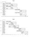
- FIG. 1 schematically shows the timing of a first particularly advantageous embodiment of the method according to the invention.
- This embodiment is particularly suitable for applying at least one reaction space with at least one voltage pulse.
- the charge storage device designated CHV2A2 is first charged here.
- This charge storage device is subsequently discharged, so that at least one first reaction space R1 is subjected to at least one voltage pulse.
- the second charge storage device CHV2A1 is charged or partially discharged parallel to the at least partial discharge of the first charge storage device CHV2A2.
- Partial discharge means that the charge storage device is placed in readiness to deliver the next or following voltage pulse, ie, the voltage level in the charge storage device is adapted to the voltage required for the next voltage pulse.
- the voltage level in the charge storage device is adapted to the new, lower voltage level for the next reaction space by partial discharge by means of a discharge device, for example via an electrical load, preferably by means of a discharge resistor. Consequently, the second charge storage device CHV2A1 is immediately available for the next discharge when the first charge storage device CHV2A2 has been discharged.
- the next discharging process can thus begin without a break immediately after the first discharging process, so that no time is required or lost between two voltage pulses for the charging or the partial discharging of a charge storage device.
- the discharge of the first charge storage device CHV2A1 immediately follows without interruption in the present exemplary embodiment.
- a further reaction space R2 is subjected to a voltage pulse in the present exemplary embodiment.
- a charge storage device Due to the simultaneous discharging and charging or partial discharging of the charge storage devices, a charge storage device is always available for generating a voltage pulse, so that the individual voltage pulses can be delivered directly one behind the other. If a large number of voltage pulses has to be emitted in succession, be it in the event that a reaction space must be subjected to a sequence of multiple voltage pulses, or if several reaction spaces each have to be subjected to a voltage pulse, then the entire process duration can be significantly reduced by the method according to the invention become.
- the inventive method is therefore particularly suitable for Electroporation, electrofusion or similar methods in flow or high throughput operation.
- “Simultaneous” charging and discharging of the charge storage devices means that the charging and discharging processes run at least partially synchronously. The loading and unloading processes can therefore take place either in parallel or at different times. "Staggered” means that one process is still running or already running while the other process has already ended or has not yet begun.
- FIG. 2 schematically shows the timing of another embodiment of the method according to the invention.
- This embodiment is particularly suitable for acting on at least two reaction chambers, each with at least one voltage pulse.
- the charge storage devices referred to herein as CHV2A2 and CHV2B2 are charged.
- These first charge storage devices are then at least partially discharged, so that at least two reaction spaces, here R1 and R2, are each subjected to a voltage pulse.
- the two second charge storage devices CHV2A1 and CHV2B1 are charged.
- “Simultaneous” in the sense of the invention means that the loading and unloading at least partially run synchronously, ie both processes can take place synchronously or at different times, in the latter case, one process is still or already running while the other process already ended is or has not started yet.
- the previously charged second charge storage devices CHV2A1 and CHV2B1 are then discharged and at the same time the previously discharged first charge storage devices CHV2A2 and CHV2B2 are recharged or partially discharged.
- the further reaction chambers R3 and R4 can each be subjected to a voltage pulse while already preparing the next voltage pulses. These steps can be repeated as often as you like.
- At least two reaction spaces can thus be charged simultaneously with one voltage pulse at a time, with the next two reaction spaces immediately thereafter can be applied with voltage pulses without time for the recharging or the partial discharge of the charge storage devices is lost.
- This is particularly advantageous when a plurality of reaction spaces with voltage pulses must be applied, since the total time that must be expended for applying all voltage pulses to all reaction chambers, is considerably shortened.
- FIG. 3 schematically shows the timing of a particular embodiment of the method according to the invention, which essentially according to the method FIG. 2 equivalent.
- the same reaction spaces R1 and R2 applied with multiple voltage pulses.
- the further reaction spaces R3 and R4 are electrically treated, in the embodiment according to FIG. 3 only the reaction chambers R1 and R2 with a plurality of successive voltage pulses applied.
- the embodiments according to FIG. 2 and FIG. 3 to combine, so that several reaction chambers can be successively applied in each case with multiple voltage pulses.
- FIG. 4 shows schematically the timing of a particularly advantageous embodiment of the method according to the invention.
- This embodiment of the method according to the invention is particularly suitable for applying at least one reaction space with at least two electrical voltage pulses.
- the charge storage device labeled CHV1A is first charged. This charge storage device is then at least partially discharged, wherein the first reaction space R1 is subjected to a voltage pulse.
- a second charge storage device CHV2A2 is charged.
- This charge storage device CHV2A2 is at least partially discharged immediately after the discharge of the first charge storage device CHV1A, hereby likewise the reaction space R1 with a corresponding voltage pulse is charged.
- the reaction space R1 is thus successively acted upon by two successive voltage pulses, wherein these two voltage pulses preferably merge without interruption directly into one another.
- the first voltage pulse may be a short pulse having a relatively high voltage amplitude and the second voltage pulse may be a longer pulse having a lower voltage amplitude.
- the two voltage pulses can be discontinued successively with a more or less short break, so that a double pulse is generated with interruption.
- the further second charge storage device CHV2A1 is charged.
- the first charge storage device CHV1A and another second charge storage device CHV2A1 are charged.
- the next reaction space R2 can be charged with a double voltage pulse. This is done first by at least partial discharging of the first charge storage device CHV1A and the directly without interruption subsequent thereto at least partial discharge of the further second charge storage device CHV2A1.
- the same reaction space R1 can also be charged with a further voltage pulse.
- the first charge storage device CHV1A and the second charge storage device CHV2A2 are again charged or partially discharged, so that the next double voltage pulse can be delivered without delay.
- the loading and unloading operations described above can be repeated as often as desired so that a large number of voltage pulses can be delivered in a relatively short time.
- the process duration is thereby also in the electrical Treatment of many reaction spaces minimized because no time is lost for the charging or the partial discharge of charge storage devices between the individual voltage pulses or the treatment of successive reaction spaces.
- FIG. 5 schematically shows the timing of another embodiment of the method according to the invention.
- This embodiment is particularly suitable for the simultaneous admission of at least two reaction spaces, each with at least two voltage pulses.
- At the beginning of the process at least four charge storage devices are initially charged simultaneously or successively. These four charge storage devices are referred to in the present embodiment as CHV1A, CHV2A2, CHV1B and CHV2B2.
- At first two first charge storage devices CHV1A and CHV1B are at least partially discharged, at least two reaction spaces, here R1 and R2, each being subjected to a voltage pulse.
- the previously charged second charge storage devices CHV2A1 and CHV2B1 are then discharged again while, in parallel, the previously discharged charge storage devices CHV2A2 and CHV2B2 are reloaded or partially discharged.
- the loading and unloading operations described above can then be repeated as often as desired, so that a great many Voltage pulses can be delivered in a relatively short time. In this way, a plurality of reaction chambers in a relatively short time with voltage pulses, in particular double pulses, are applied.
- FIG. 6 schematically shows the timing of a particular embodiment of the method according to the invention, which is substantially the embodiment according to FIG. 5 equivalent.
- the respective first voltage pulses of a double voltage pulse are not generated simultaneously (synchronously), but one after the other. This means that the discharge of the first charge storage devices CHV1A and CHV1B takes place in succession, so that the reaction spaces R1 and R2 or R3 and R4 are not acted upon at the same time but in succession with the first voltage pulses.
- the respective second voltage pulses of a double voltage pulse are delivered not parallel, but slightly offset and overlapping.
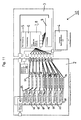
- FIG. 7 shows schematically the structure of an embodiment of the device according to the invention for applying at least one reaction space with at least one voltage pulse.
- the device 1 according to the invention has a substantially modular structure and consists at least of a power supply module 2, a pulse distribution module 3 and a control module 4.
- the control module 4 comprises a control unit comprising a microprocessor, and may for example be a conventional personal computer, preferably a laptop.
- the pulse distribution module 3 comprises a container control device 5, which includes the controller for the container, which includes the reaction space or the reaction spaces.
- the pulse distribution module 3 further comprises a central control device 6 (main controller), which controls the distribution of the individual voltage pulses to the reaction space or the reaction spaces.
- the pulse distribution module 3 also has a pulse generation unit 7 and a switching unit 8.
- the pulse generation unit 7 includes components that enable the transition of successive voltage pulses, such as a mixed circuit including analog and digital components.
- the switching unit 8 comprises the measurement circuits for the voltage pulses and the switches (eg IGBTs or MOSFETs) for the discharge of the charge storage devices.
- the switching unit 8 is coupled to the distribution device 9 for electrical voltage pulses.
- the distribution device 9 comprises the switching devices (eg relays) for distributing the voltage pulses and the mechanical means for moving and positioning the container (s) comprising the reaction spaces.
- the power supply module 2 according to the in FIG. 7 illustrated embodiment of the device 1 according to the invention essentially comprises two charge storage devices 10, 11, which can be loaded by a common power supply device 12.
- the power supply device 12 is controlled by the power supply controller 15. Furthermore, at least one unloading device, not shown here, is provided, via which the charge storage devices 10, 11 can be partially unloaded.
- the discharge device may be, for example, a discharge resistor.
- the power supply module 2 further comprises a central power supply 13, which ensures the voltage supply in the entire device 1.
- the two charge storage devices 10, 11 form a storage module, which is connected to the pulse distribution module 3 via a common interface 14.
- the memory module ie the charge storage devices 10 and 11, are thus electrically coupled in the present embodiment via the pulse generation unit 7 and the switching unit 8 with the distribution device 9.
- the two charge storage devices 10, 11 form a storage module in which one of the two charge storage devices 10, 11 is always charged by the voltage supply device 12, while the other charge storage device 10, 11 is charged or dischargeable, the storage module stands in total to each Time to provide a voltage pulse available.
- the charge storage devices 10, 11 may be, for example, individual capacitors or in each case around entire capacitor banks, which consist of a plurality of capacitors connected in parallel and / or in series.
- high voltages in particular of more than 1000 V is connected on the part of the electronics with a certain effort, since special voltage-proof components must be used and certain distances between the high-voltage conductor tracks must be maintained on the board to a high To ensure dielectric strength of the electronics.
- high-voltage power supplies are particularly complex and expensive to produce, which can provide the required charge for the electroporation corresponding charge and thus power levels at high voltages.
- U charging charging voltage
- FIG. 8 schematically shows the structure of another embodiment of a device according to the invention.
- the device 20 is particularly suitable for applying at least one reaction space with at least two voltage pulses.
- the device 20 corresponds in terms of the modular structure and the essential components of the device 1 according to FIG. 7 , Because of this, are in FIG. 8 the same components are marked with the same reference numerals as in FIG. 7 ,
- the device 20 according to the invention FIG. 8 differs from the device 1 according to FIG. 7 in that a further charge storage device 21 is provided, which is coupled to the distribution device 9 via a further interface 22.
- the charge storage device 21 is fed by a further voltage supply device 23 and allows the loading of the reaction space or the reaction chambers with double, briefly successive or without interruption merging voltage pulses.
- This embodiment is particularly advantageous when voltage pulses are to be generated, which are composed of a short voltage pulse, preferably with a relatively high voltage amplitude, and a longer voltage pulse, preferably with a lower voltage amplitude.
- the charge storage device 21 may generate a short voltage pulse while that from the charge storage devices 10 and 11 composing memory module provides a longer voltage pulse.
- the pulse generation unit 7 if a plurality of reaction spaces are to be acted upon successively in a relatively short time by such double voltage pulses, for example when using multiwell plates in the high-throughput process, the distances between the application of the individual would be the same Reaction spaces when using a single capacitor for the longer voltage pulse relatively long, since the capacitor would have to be recharged after unloading.
- one of the two charge storage devices 10, 11 can always be at least partially discharged, while the other charge storage device 10, 11 is charged or partially discharged, so that very many reaction spaces can be subjected to voltage pulses within a short time.
- the charging or partial discharging of the charge storage device 21 is not a time-limiting factor, since the charge storage device 21 can be charged or partially discharged during the prolonged discharge of the memory module.
- FIG. 9 schematically shows the structure of another embodiment of the device according to the invention, this embodiment is particularly suitable for carrying out the method according to the invention for acting on at least two reaction chambers, each with an electrical voltage pulse.
- the inventive device 30 also corresponds to the device 1 according to the modular structure and the essential components FIG. 7 , wherein the same components are also marked here with the same reference numerals.
- the device 30 according to the invention differs from the device 1 according to FIG. 7 in that the power supply module 2 comprises two additional charge storage devices 31, 32 and an additional voltage supply device 33.
- the charge storage devices 31, 32 form a storage module that can be charged by the common power supply 33 and via the common interface 34 and the pulse generation unit 7 or the switching unit 8 is electrically coupled to the distribution device 9.
- the charge storage devices 10, 11, 31, 32 form a total of two memory modules, which can be discharged at any time, can be acted upon by the device 30 according to the invention always two reaction chambers simultaneously with one voltage pulse. Since, as described above, no time is required for the charging of a single capacitor between two consecutive voltage pulses, by means of the device 30 according to the invention consequently very many reaction spaces can be subjected to voltage pulses in a relatively short time.
- the device 30 according to the invention is therefore particularly suitable for use in high-throughput processes, in which a large number of reaction spaces must be acted upon in each case with a voltage pulse in a short time.
- FIG. 10 schematically shows a further embodiment of the device according to the invention, which in principle consists of the components of the device 20 according to the invention FIG. 8 and the device 30 according to the invention FIG. 9 composed. Consequently, here too, the same components are identified by the same reference numerals.
- the device 40 according to the invention additionally comprises a further charge storage device 41, which can be charged by its own power supply device 42 and is electrically coupled to the distribution device 9 via its own interface 43.
- the device 40 according to the invention thus has, within the power supply module 2, a total of 6 charge storage devices 10, 11, 21, 31, 32, 41, which are coupled to the distribution device 9 via a total of four interfaces 14, 22, 34, 43.
- charge storage devices 10 and 11 or 31 and 32 form a total of two memory modules, which can be discharged at any time as described above.
- the charge storage devices 10, 11, 21, 31, 32, 41 are charged via a total of four voltage supply devices 12, 23, 33, 42, each voltage supply device 12, 33 being assigned to each memory module.
- the device 40 according to the invention can be used particularly advantageously in high-throughput processes in which many reaction spaces have to be subjected to double voltage pulses in a short time. In this case, by means of the device 40 according to the invention always two reaction chambers can be acted upon simultaneously with voltage pulses.
- the charge storage devices 21 and 41 can simultaneously deliver a short voltage pulse with a relatively high voltage amplitude, which then passes without interruption into a longer voltage pulse with a lower voltage amplitude.
- the longer voltage pulses can be made available by the two memory modules, wherein one of the two charge storage devices 10, 11 or 31, 32 of a memory module can always be discharged.
- the assembling of the double voltage pulse takes place in this embodiment in the pulse generation unit 7.
- FIG. 11 shows a further particular embodiment of the device according to the invention, the structure in principle of the device 40 according to FIG. 10 equivalent.
- the device 50 according to FIG. 11 lies in accordance with the device 50 according to the invention FIG. 11 a doubling of the components of the power supply module 2 before. Consequently, with the device 50 according to the invention four reaction chambers can be acted upon simultaneously with voltage pulses.
- the device 50 according to the invention additionally comprises two further memory modules, which are formed by the charge storage devices 51 and 52 or 53 and 54, wherein the two additional memory modules are electrically coupled to the distribution device 9 via an interface 55 and 56, respectively. Each additional memory module is charged via its own power supply device 57 or 58.
- two further charge storage devices 60 and 63 are provided, which are each coupled via a separate interface 61 and 64 to the distribution device 9 and each have their own power supply means 62 and 65, respectively can be loaded.
- the device 50 according to the invention can therefore in comparison to the device 40 according to FIG. 10 either significantly reduces the time for charging the same number of reaction spaces or significantly increases the number of reaction spaces to be treated.
- the number of charge storage devices or memory modules can be further increased to be able to apply even more reaction spaces simultaneously with voltage pulses.
- FIG. 12 schematically shows a particular embodiment of the device according to the invention, which is substantially the inventive device 40 according to FIG. 10 equivalent. Therefore, the same components are marked with the same reference numbers here.
- the device 70 according to FIG. 12 differs from the embodiment according to FIG. 10 in that here the pulse generation unit 7 is arranged within the power supply module 2.
- the pulse generation unit 7 is therefore not arranged in this embodiment as a unit with the switching unit 8 within the pulse distribution module 3.
- the charge storage devices 10, 11, 21, 31, 32, 41 are therefore directly coupled to the pulse regeneration unit 7 in this embodiment. This has the advantage that in this case the double-voltage pulse applied to the individual reaction chambers can already be assembled in the power supply module 2 before the voltage pulse is transmitted to the distribution device 9 via the switching unit 8.
- the double voltage pulse is generated from the first voltage pulse provided by the charge storage device 21 or 41 and the second voltage pulse provided by the charge storage devices 10 and 11 or 31 and 32, respectively.
- the complete double voltage pulse is then passed through the interfaces 71 and 72 or 73 and 74 to the switching unit 8.
- the pulse generation unit 7 may comprise a mixed circuit including analog and digital components through which the first and second voltage pulses may be coupled together to form a double voltage pulse.
- Particularly advantageous in this embodiment is the reduction of the between the units to leading high voltage cables. Since these cables and the associated connection technology are complex, thereby the overall complexity can be reduced and the reliability can be increased, especially for the high-throughput operation.
Landscapes
- Health & Medical Sciences (AREA)
- Life Sciences & Earth Sciences (AREA)
- Engineering & Computer Science (AREA)
- Chemical & Material Sciences (AREA)
- Bioinformatics & Cheminformatics (AREA)
- Organic Chemistry (AREA)
- Zoology (AREA)
- Wood Science & Technology (AREA)
- Genetics & Genomics (AREA)
- Biotechnology (AREA)
- Biomedical Technology (AREA)
- General Engineering & Computer Science (AREA)
- Microbiology (AREA)
- Biochemistry (AREA)
- General Health & Medical Sciences (AREA)
- Sustainable Development (AREA)
- Cell Biology (AREA)
- Physics & Mathematics (AREA)
- Electromagnetism (AREA)
- Biophysics (AREA)
- Plant Pathology (AREA)
- Virology (AREA)
- Molecular Biology (AREA)
- Medicinal Chemistry (AREA)
- Apparatus Associated With Microorganisms And Enzymes (AREA)
- Physical Or Chemical Processes And Apparatus (AREA)
Priority Applications (5)
| Application Number | Priority Date | Filing Date | Title |
|---|---|---|---|
| EP09000698A EP2208778A1 (fr) | 2009-01-20 | 2009-01-20 | Procédé et dispositif destinés au traitement électrique d'espaces de réaction |
| KR1020117018976A KR101761925B1 (ko) | 2009-01-20 | 2010-01-20 | 반응 공간의 전기적 처리를 위한 방법 및 장치 |
| US13/145,113 US9249384B2 (en) | 2009-01-20 | 2010-01-20 | Method and device for the electrical treatment of reaction spaces |
| JP2011545701A JP5926560B2 (ja) | 2009-01-20 | 2010-01-20 | 反応空間の電気的処理のための方法及び装置 |
| PCT/EP2010/000295 WO2010083985A2 (fr) | 2009-01-20 | 2010-01-20 | Procédé et dispositif destinés au traitement électrique d'espaces de réaction |
Applications Claiming Priority (1)
| Application Number | Priority Date | Filing Date | Title |
|---|---|---|---|
| EP09000698A EP2208778A1 (fr) | 2009-01-20 | 2009-01-20 | Procédé et dispositif destinés au traitement électrique d'espaces de réaction |
Publications (1)
| Publication Number | Publication Date |
|---|---|
| EP2208778A1 true EP2208778A1 (fr) | 2010-07-21 |
Family
ID=40823617
Family Applications (1)
| Application Number | Title | Priority Date | Filing Date |
|---|---|---|---|
| EP09000698A Withdrawn EP2208778A1 (fr) | 2009-01-20 | 2009-01-20 | Procédé et dispositif destinés au traitement électrique d'espaces de réaction |
Country Status (5)
| Country | Link |
|---|---|
| US (1) | US9249384B2 (fr) |
| EP (1) | EP2208778A1 (fr) |
| JP (1) | JP5926560B2 (fr) |
| KR (1) | KR101761925B1 (fr) |
| WO (1) | WO2010083985A2 (fr) |
Families Citing this family (1)
| Publication number | Priority date | Publication date | Assignee | Title |
|---|---|---|---|---|
| US9450369B2 (en) * | 2014-11-26 | 2016-09-20 | Convergent Dental, Inc. | Systems and methods for supplying power to and cooling dental laser systems |
Citations (5)
| Publication number | Priority date | Publication date | Assignee | Title |
|---|---|---|---|---|
| WO1991018103A1 (fr) * | 1990-05-16 | 1991-11-28 | Scientific Equipment Design & Development S.C. | Procede et dispositif de permeabilisation de cellules vivantes |
| US6010613A (en) | 1995-12-08 | 2000-01-04 | Cyto Pulse Sciences, Inc. | Method of treating materials with pulsed electrical fields |
| US6150148A (en) | 1998-10-21 | 2000-11-21 | Genetronics, Inc. | Electroporation apparatus for control of temperature during the process |
| EP1577378A1 (fr) * | 2004-03-15 | 2005-09-21 | Amaxa GmbH | Récipient et installation destinée a creer des champs électriques dans des espaces de réaction independents |
| EP1961807A1 (fr) * | 2007-02-23 | 2008-08-27 | Amaxa AG | Procédé et dispositif destinés à la stabilisation du fleuve par une chambre |
Family Cites Families (10)
| Publication number | Priority date | Publication date | Assignee | Title |
|---|---|---|---|---|
| DE10031179A1 (de) | 2000-06-27 | 2002-01-31 | Amaxa Gmbh | Verfahren zur Einbringung von Nukleinsäuren und anderen biologisch aktiven Molekülen in den Kern höherer eukaryontischer Zellen mit Hilfe elektrischen Stroms |
| EP1427837B1 (fr) | 2001-01-10 | 2011-10-26 | Lonza Cologne GmbH | Systèmes de transfection modulaires à base de filaments de nucléoproteines |
| DE10119901A1 (de) | 2001-04-23 | 2002-10-24 | Amaxa Gmbh | Schaltungsanordnung zur Einbringung von Nukleinsäuren und anderen biologisch aktiven Molekülen in den Kern höherer eukaryontischer Zellen mit Hilfe elektrischen Stroms |
| AU2003206415A1 (en) | 2002-01-07 | 2003-07-24 | Uab Research Foundation | Electroporation cuvette-pipette tips, multi-well cuvette arrays, and electrode template apparatus adapted for automation and uses thereof |
| US7371561B2 (en) | 2003-10-28 | 2008-05-13 | Cyto Pulse Sciences | In vitro, multiple electrode pair array and multiple treatment cell apparatus for use in electroporation |
| US7923238B2 (en) * | 2006-02-10 | 2011-04-12 | Bio-Rad Laboratories, Inc. | Multi-channel electroporation system |
| US7799555B2 (en) | 2006-02-10 | 2010-09-21 | Bio-Rad Laboratories, Inc. | Apparatus for high-throughput electroporation |
| US7750605B2 (en) | 2006-09-21 | 2010-07-06 | Bio-Rad Laboratories, Inc. | Controlling an electrical signal sent to a sample load using a pulse modulated resistance |
| ES2657700T3 (es) | 2009-01-20 | 2018-03-06 | Lonza Cologne Gmbh | Procedimiento y dispositivo para el tratamiento eléctrico de varios recipientes |
| EP2208779B1 (fr) | 2009-01-20 | 2017-04-05 | Lonza Cologne GmbH | Récipient doté de plusieurs espaces de réaction et électrodes |
-
2009
- 2009-01-20 EP EP09000698A patent/EP2208778A1/fr not_active Withdrawn
-
2010
- 2010-01-20 WO PCT/EP2010/000295 patent/WO2010083985A2/fr active Application Filing
- 2010-01-20 US US13/145,113 patent/US9249384B2/en active Active
- 2010-01-20 KR KR1020117018976A patent/KR101761925B1/ko active IP Right Grant
- 2010-01-20 JP JP2011545701A patent/JP5926560B2/ja active Active
Patent Citations (5)
| Publication number | Priority date | Publication date | Assignee | Title |
|---|---|---|---|---|
| WO1991018103A1 (fr) * | 1990-05-16 | 1991-11-28 | Scientific Equipment Design & Development S.C. | Procede et dispositif de permeabilisation de cellules vivantes |
| US6010613A (en) | 1995-12-08 | 2000-01-04 | Cyto Pulse Sciences, Inc. | Method of treating materials with pulsed electrical fields |
| US6150148A (en) | 1998-10-21 | 2000-11-21 | Genetronics, Inc. | Electroporation apparatus for control of temperature during the process |
| EP1577378A1 (fr) * | 2004-03-15 | 2005-09-21 | Amaxa GmbH | Récipient et installation destinée a creer des champs électriques dans des espaces de réaction independents |
| EP1961807A1 (fr) * | 2007-02-23 | 2008-08-27 | Amaxa AG | Procédé et dispositif destinés à la stabilisation du fleuve par une chambre |
Also Published As
| Publication number | Publication date |
|---|---|
| JP2012515529A (ja) | 2012-07-12 |
| US20120077245A1 (en) | 2012-03-29 |
| KR101761925B1 (ko) | 2017-07-26 |
| KR20110117162A (ko) | 2011-10-26 |
| WO2010083985A2 (fr) | 2010-07-29 |
| US9249384B2 (en) | 2016-02-02 |
| JP5926560B2 (ja) | 2016-05-25 |
| WO2010083985A3 (fr) | 2011-03-31 |
Similar Documents
| Publication | Publication Date | Title |
|---|---|---|
| EP1827591B1 (fr) | Dispositif pour reguler la charge electrique au niveau d'electrodes de stimulation | |
| DE3317415A1 (de) | Kammer zur behandlung von zellen im elektrischen feld | |
| EP3373407B1 (fr) | Procédé de fonctionnement d'un système d'accumulateur modulaire, système d'accumulateur modulaire et système de gestion de batterie associé | |
| EP0148380B1 (fr) | Procédé de traitement par des impulsions électriques et dispositif de traitement des matières | |
| EP2412094B1 (fr) | Circuiterie et procédé pour fournir à un composant fonctionnel à haute énergie des impulsions de haute tension | |
| DE19513441B4 (de) | Verfahren zur Erzeugung einer Prüfspannung für die Prüfung elektrischer Betriebsmittel sowie Schaltungsanordnung zur Ausführung des Verfahrens | |
| EP2208778A1 (fr) | Procédé et dispositif destinés au traitement électrique d'espaces de réaction | |
| EP1141230B1 (fr) | Procede et dispositif pour la permeation d'objets biologiques | |
| EP3671805B1 (fr) | Dispositif et procédé de revêtement et en particulier de revêtement plasma des récipients | |
| EP3362810B1 (fr) | Moyen de déplacement, dispositif et procédé de détermination d'une tension d'une cellule d'une chaîne de plusieurs cellules connectées en série d'un accumulateur d'énergie électrochimique | |
| EP2310902B1 (fr) | Circuit de commande pour cellule de pockels | |
| EP1607484B1 (fr) | Méthode et circuits pour le traitement de matériel biologique | |
| DE102019125014A1 (de) | Verfahren zum Überwachen von Batteriezellen einer Batterie, Batteriesystem sowie Kraftfahrzeug | |
| EP2208780B1 (fr) | Procédé et dispositif destinés au traitement électrique de plusieurs récipients | |
| DE102009008373A1 (de) | Verfahren zum Kondensator-Entladungssschweißen zur Verbindung metallischer Bauteile und Schweißeinheit zur Durchführung des Verfahrens | |
| DE102018216127A1 (de) | Batteriesystem und Verfahren zum Betreiben eines Batteriesystems | |
| EP2446503A1 (fr) | Procédé et dispositif pour charger des cellules au lithium-cobalt | |
| WO2023235909A1 (fr) | Procédé de vieillissement artificiel d'une batterie et procédé de test pour tester des ensembles batteries | |
| EP1741778A1 (fr) | Procédure de traitement de faibles volumes avec l'électricité électrique | |
| WO2022058117A1 (fr) | Procédé de décharge de condensateurs de suppression d'un réseau d'alimentation en énergie non mis à la terre | |
| DE102022206877A1 (de) | Betreiben einer Elektrolysezelle | |
| DE102022127381A1 (de) | Dual-chemistry-antriebssystem für elektrische senkrechtstart- und -landeflugzeuge | |
| DE102021103989A1 (de) | Verfahren zum Überwachen von Batteriezellen einer Primärbordnetzbatterie, Bordnetz sowie Kraftfahrzeug | |
| DE19837126B4 (de) | Verfahren und Vorrichtung zur elektrischen oder elektrochemischen Manipulation von Proben | |
| DE102021212734A1 (de) | Ladestation zum Laden von Batterien, insbesondere von Kraftfahrzeugen |
Legal Events
| Date | Code | Title | Description |
|---|---|---|---|
| PUAI | Public reference made under article 153(3) epc to a published international application that has entered the european phase |
Free format text: ORIGINAL CODE: 0009012 |
|
| AK | Designated contracting states |
Kind code of ref document: A1 Designated state(s): AT BE BG CH CY CZ DE DK EE ES FI FR GB GR HR HU IE IS IT LI LT LU LV MC MK MT NL NO PL PT RO SE SI SK TR |
|
| AX | Request for extension of the european patent |
Extension state: AL BA RS |
|
| RAP1 | Party data changed (applicant data changed or rights of an application transferred) |
Owner name: LONZA COLOGNE GMBH |
|
| 17P | Request for examination filed |
Effective date: 20110120 |
|
| 17Q | First examination report despatched |
Effective date: 20110211 |
|
| AKX | Designation fees paid |
Designated state(s): AT BE BG CH CY CZ DE DK EE ES FI FR GB GR HR HU IE IS IT LI LT LU LV MC MK MT NL NO PL PT RO SE SI SK TR |
|
| STAA | Information on the status of an ep patent application or granted ep patent |
Free format text: STATUS: THE APPLICATION IS DEEMED TO BE WITHDRAWN |
|
| 18D | Application deemed to be withdrawn |
Effective date: 20130801 |