EP2207262A2 - Clocked d-type flip flop circuit - Google Patents
Clocked d-type flip flop circuit Download PDFInfo
- Publication number
- EP2207262A2 EP2207262A2 EP09175591A EP09175591A EP2207262A2 EP 2207262 A2 EP2207262 A2 EP 2207262A2 EP 09175591 A EP09175591 A EP 09175591A EP 09175591 A EP09175591 A EP 09175591A EP 2207262 A2 EP2207262 A2 EP 2207262A2
- Authority
- EP
- European Patent Office
- Prior art keywords
- switching element
- type transistor
- output
- switching
- output signal
- Prior art date
- Legal status (The legal status is an assumption and is not a legal conclusion. Google has not performed a legal analysis and makes no representation as to the accuracy of the status listed.)
- Withdrawn
Links
Images




Classifications
-
- H—ELECTRICITY
- H03—ELECTRONIC CIRCUITRY
- H03K—PULSE TECHNIQUE
- H03K3/00—Circuits for generating electric pulses; Monostable, bistable or multistable circuits
- H03K3/02—Generators characterised by the type of circuit or by the means used for producing pulses
- H03K3/353—Generators characterised by the type of circuit or by the means used for producing pulses by the use, as active elements, of field-effect transistors with internal or external positive feedback
- H03K3/356—Bistable circuits
- H03K3/356104—Bistable circuits using complementary field-effect transistors
- H03K3/356113—Bistable circuits using complementary field-effect transistors using additional transistors in the input circuit
- H03K3/356121—Bistable circuits using complementary field-effect transistors using additional transistors in the input circuit with synchronous operation
-
- H—ELECTRICITY
- H03—ELECTRONIC CIRCUITRY
- H03K—PULSE TECHNIQUE
- H03K3/00—Circuits for generating electric pulses; Monostable, bistable or multistable circuits
- H03K3/02—Generators characterised by the type of circuit or by the means used for producing pulses
- H03K3/353—Generators characterised by the type of circuit or by the means used for producing pulses by the use, as active elements, of field-effect transistors with internal or external positive feedback
- H03K3/356—Bistable circuits
- H03K3/356104—Bistable circuits using complementary field-effect transistors
- H03K3/356113—Bistable circuits using complementary field-effect transistors using additional transistors in the input circuit
- H03K3/356147—Bistable circuits using complementary field-effect transistors using additional transistors in the input circuit using pass gates
- H03K3/356156—Bistable circuits using complementary field-effect transistors using additional transistors in the input circuit using pass gates with synchronous operation
Definitions
- the present invention relates to a clocked D-type Flip-Flop circuit.
- a clocked D-type Flip-Flop receives an input D (data) but the output Q does not response to the transition in the input D unless there is a transition in the state of a clock.
- the rising edge or the upward transition of the clock enables the transition of the output Q dependent upon whether a transition in D also occurs.
- the state of the output Q is dependent upon the state of D when the upward transition of the clock occurs.
- the present invention provides a clocked D-type Flip-Flop circuit which has a transmission gate to admit an input data and to provide an intermediate output to a clock-controlled inverter based on the clock signals.
- the clock-controlled inverter is used as a latch for latching the output signal from the transmission gate and releases the latched signal by the same clock signals to an output inverter.
- the output of the output inverter is the Q terminal of the Flip-Flop circuit.
- Another output inverter is used to invert the signal from the Q terminal into a complementary output signal.
- another transmission gate is used to condition the complementary output signal.
- the clock-controlled inverter can be a switching series having a first series end and an opposing second series end, the first series end connected to a first voltage source (VDD) and the second series end connected to a second voltage level source (GND) different from the first voltage level source, the switching series comprising a plurality of switching elements (M3-M6) connected in series, wherein the plurality of switching elements comprise:
- the clocked D-type Flip-Flop circuit comprises a transmission gate to admit an input D (data) and to provide an intermediate output to a clock-controlled inverter (or a push-pull section) based on the clock signals.
- the clock-controlled inverter in response to the immediate output from the transmission gate and the clock signals, provides an output to an output inverter.
- the clocked D-type Flip-Flop circuit 10 comprises a transmission gate 20, a clock-controlled inverter 30 and an output inverter 40.
- All the switching elements in the transmission gate 20, the clock-controlled inverter 30 and the output inverter 40 are MOS (Metal-Oxide-Semiconductor) FETs (Field Effect Transistors).
- the transmission gate 20 comprises an n-MOS transistor M1 and a p-MOS transistor M2.
- the source (S) of the n-MOS transistor M1 is connected to the drain (D) of the p-MOS transistor M2.
- the drain of the n-MOS transistor M1 is connected to the source of the p-MOS transistor M2.
- the input D is received at the source of the n-MOS transistor M1 .
- the gate of the n-MOS transistor M1 is configured to receive a clock signal CLK and the gate of p-MOS transistor M2 is configured to receive a complementary clock signal CKB.
- the output of the transmission gate 20 is provided at the drain of the n-MOS transistor M1 to a node N01 .
- the clock-controlled inverter 30 comprises a plurality of switching elements connected in series.
- the clock-controlled inverter 30 comprises a first transistor M3 connected to a first voltage level, such as VDD, a second transistor M4 connected to the first transistor M3, a third transistor M5 connected to the second transistor M4, and a fourth transistor M6 connected between the third transistor M5 and a second voltage level, such as GND.
- the first transistor M3 and the second transistor M4 are p-MOS transistors
- the third transistor M5 and the fourth transistor M6 are n-MOS transistors.
- the drain of the first transistor M3 is connected to VDD
- the drain of the second transistor M4 is connected to the source of the first transistor M3
- the source of the third transistor MS is connected to the source of the second transistor M4
- the source of the fourth transistor M6 is connected to the drain of the third transistor M5
- the drain of the fourth transistor M6 is connected to GND.
- the gate of the first transistor M3 and the gate of the fourth transistor M6 are configured to receive the output of the transmission gate 20 at the node N01 .
- the gate of the second transistor M4 is configured to receive the clock signal CLK and the gate of the third transistor M5 is configured to receive the complementary clock signal CKB.
- the output of the clock-controlled inverter 30 is provided to the output inverter 40 from a node N05 .
- the output inverter 40 comprises two switching elements, p-MOS transistor M7 and n-MOS transistor M8, connected in series. As shown in Figure 3 , the drain of the p-MOS transistor M7 is connected to VDD, and the drain of the n-MOS transistor M8 is connected to GND. The source of the n-MOS transistor M8 is connected to the source of the p-MOS transistor M7 for providing the output Q of the output inverter 40. The gate of the transistor M7 is connected to the gate of the transistor M8 for receiving an input signal from node N05. The state of the output Q is complementary to the state of the signal at node N05.
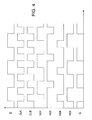
- the signal levels at various nodes in the circuit are shown in the time chart of Figure 4 .
- the node N03 is located between M3 and M4 of the clock-controlled inverter 30 and the node N04 is located between M5 and M6.
- Figure 5 shows a clocked D-type Flip-Flop circuit, according to another embodiment of the present invention.
- a complementary output QB is provided from another output inverter 50.
- the output Q of the output inverter 40 is provided to the output inverter 50.
- the state of the output QB is complementary to the state of signal Q.
- FIG. 6 shows a clocked D-type Flip-Flop circuit, according to yet another embodiment of the present invention.
- the Flip-Flop circuit as shown in Figure 6 is similar to the circuit shown in Figure 5 , except that another transmission gate 60 is provided between node N05 and the output QB of the output inverter 50.
- the transmission gate 60 comprises an n-MOS transistor M11 and a p-MOS transistor M12.
- the source of the n-MOS transistor M11 is connected to the drain of the p-MOS transistor M12 for receiving an input signal from node N05 .
- the drain of the n-MOS transistor M11 is connected to the source of the p-MOS transistor M12 for providing an output signal to the output terminal of the output inverter 50.
- the gate of the n-MOS transistor M11 is configured to receive a clock signal CLK and the gate of p-MOS transistor M12 is configured to receive a complementary clock signal CKB .
- the adoption of n-MOS transistor M11 and p-MOS transistor M12 can avoid node N05 from floating, and prevent the transistors M7, M8, M9 and M10 from working in an unstable state. That is, the use of transmission gate 60 can reduce the noise disturbance and increase the noise immunity.
- the present invention provides a clocked D-type Flip-Flop circuit, which comprises: a transmission gate, a clock controlled inverter and an output converter.
- the transmission gate provides an intermediate signal, in response to an input data and complementary clock signals, to the clock controlled inverter which has four switches connected in series in a switching series.
- the transmission gate comprises an input end for receiving an input signal (D) and an output end (N01) for providing a first output signal in response to the input signal, the transmission gate configured for receiving a first clock signal (CLK) and a second clock signal (CKB) complementary to the first clock signal for controlling the first output signal.
- CLK first clock signal
- CKB second clock signal
- the switching series has a first series end and an opposing second series end, the first series end connected to a first voltage source (VDD) and the second series end connected to a second voltage level source (GND) different from the first voltage level source, the switching series comprising a plurality of switching elements (M3-M6) connected in series, wherein the plurality of switching elements comprise:
- the Flip-Flop circuit also has a module electrically connected to the first output point for providing a third output signal (Q) in response to the second output signal.
- the module comprises a converter circuit such that the third output signal is complementary to the second output signal.
- the first switching element comprises a p-type transistor having a gate terminal arranged for receiving the first output signal; the second switching element comprises a p-type transistor having a gate terminal arranged for receiving the first clock signal; the third switching element comprises an n-type transistor having a gate terminal arranged for receiving the second clock signal; and the fourth switching element comprises an n-type transistor having a gate terminal arranged for receiving the first output signal.
- the transmission gate comprises: an n-type transistor (M1) having a first drain terminal electrically connected to the output end (N01) of the transmission gate, a first source terminal electrically connected to the input end of the transmission gate, and a first gate terminal arranged for receiving the first clock signal; and a p-type transistor (M2) having a second source terminal electrically connected to the first drain terminal, a second drain terminal electrically connected to the first source terminal, and a second gate terminal arranged for receiving the second clock signal.
- M1 n-type transistor
- M2 p-type transistor having a second source terminal electrically connected to the first drain terminal, a second drain terminal electrically connected to the first source terminal, and a second gate terminal arranged for receiving the second clock signal.
- the converter circuit comprises: a p-type transistor (M7) electrically connected to the first voltage level source (VDD); and an n-type transistor (M8) connected between the p-type transistor and the second voltage level input (GND), wherein each of the p-type transistor (M7) and the n-type transistor (M8) has a gate terminal arranged for receiving the second output signal, and wherein the converter circuit further comprises a second output point between the p-type transistor and the n-type transistor for providing the third output signal (Q).
- the Flip-Flop circuit also includes a second converter circuit electrically connected to the second output point for providing a fourth output signal (QB) in response to the third output signal (Q) such that the fourth output signal is complementary to the third output signal.
- the second converter circuit comprises: a second p-type transistor (M9) electrically connected to the first voltage level input (VDD); and a second n-type transistor (M10) connected between the second p-type transistor and the second voltage level input (GND), wherein each of the second p-type transistor (M9) and the second n-type transistor (M10) has a second gate terminal arranged for receiving the second output signal, and wherein the second converter circuit further comprises a third output point between the second p-type transistor and the second n-type transistor for providing the fourth output signal (QB).
- the Flip-Flop circuit further includes a second transmission gate (60), the second transmission gate arranged to receive the first clock signal (CLK) and the second clock signal (CKB), wherein the second transmission gate comprises a first gate end connected to the first output point (N05) for receiving the second output signal, and a second gate end connected to the third output point in the second converter circuit (50).
- CLK first clock signal
- CKB second clock signal
- the second transmission gate comprises: an n-type transistor (M11) having a drain terminal electrically connected to the third output point of the second converter circuit, a source terminal electrically connected to the first gate end, and a gate terminal arranged for receiving the first clock signal; and a p-type transistor (M12) having a source terminal electrically connected to the drain terminal of the n-type transistor in the second transmission gate, a drain terminal electrically connected to the source terminal of the n-type transistor in the second transmission gate, and a second gate terminal arranged for receiving the second clock signal.
- M11 n-type transistor
- M12 p-type transistor
Landscapes
- Logic Circuits (AREA)
- Shift Register Type Memory (AREA)
Abstract
Description
- The present invention relates to a clocked D-type Flip-Flop circuit.
- As known in the art, a clocked D-type Flip-Flop receives an input D (data) but the output Q does not response to the transition in the input D unless there is a transition in the state of a clock. Conventionally, the rising edge or the upward transition of the clock enables the transition of the output Q dependent upon whether a transition in D also occurs. Furthermore, the state of the output Q is dependent upon the state of D when the upward transition of the clock occurs. The inputs and outputs of a clocked D-type Flip-Flop chip is shown in
Figure 1 , and a timing chart showing the relations between the input D, the clock CLK and the output Q is shown inFigure 2 . - The present invention provides a clocked D-type Flip-Flop circuit which has a transmission gate to admit an input data and to provide an intermediate output to a clock-controlled inverter based on the clock signals. The clock-controlled inverter is used as a latch for latching the output signal from the transmission gate and releases the latched signal by the same clock signals to an output inverter. The output of the output inverter is the Q terminal of the Flip-Flop circuit. Another output inverter is used to invert the signal from the Q terminal into a complementary output signal. In one of the embodiments of the present invention, another transmission gate is used to condition the complementary output signal.
- The clock-controlled inverter can be a switching series having a first series end and an opposing second series end, the first series end connected to a first voltage source (VDD) and the second series end connected to a second voltage level source (GND) different from the first voltage level source, the switching series comprising a plurality of switching elements (M3-M6) connected in series, wherein the plurality of switching elements comprise:
- a first switching element (M3) at the first series end;
- a second switching element (M4) electrically connected to the first switching element;
- a third switching element (M5) electrically connected to the second switching element; and
- a fourth switching element (M6) electrically connected between the third switching element and the second series end, wherein each of the first switching element, the second switching element, the third switching element and the fourth switching element is operable in two complementary switching states, and wherein
- the first output signal is arranged to cause the first switching element and the fourth switching element to operate between said two switching states, such that the switching states of the first switching element are complementary to the switching states of the fourth switching element;
- the first clock signal is arranged to cause the second switching element to operate between said two switching states; and the second clock signal is arranged to cause the third switching element to operate between said two switching states, such that the switching states of the second switching element are the same as the switching states of the third switching element, and wherein the switching series is configured to provide a second output signal at a first output point (N05) between the second switching and third switching element.
- The present invention will become apparent upon reading the description taken in conjunction with
Figures 1 to 6 . -
-
Figure 1 shows a clocked D-type Flip-Flop chip. -
Figure 2 shows a time chart for a clocked D-type Flip-Flop circuit. -
Figure 3 shows a clocked D-type Flip-Flop circuit, according to one embodiment of the present invention. -
Figure 4 is a timing chart showing typical signal levels at various nodes of the clocked D-type Flip-Flop circuit, according to various embodiments of the present invention. -
Figure 5 shows a clocked D-type Flip-Flop circuit, according to another embodiment of the present invention. -
Figure 6 shows a clocked D-type Flip-Flop circuit, according to yet another embodiment of the present invention. - The clocked D-type Flip-Flop circuit, according to various embodiments of the present invention, comprises a transmission gate to admit an input D (data) and to provide an intermediate output to a clock-controlled inverter (or a push-pull section) based on the clock signals. The clock-controlled inverter, in response to the immediate output from the transmission gate and the clock signals, provides an output to an output inverter. As shown in
Figure 3 , the clocked D-type Flip-Flop circuit 10 comprises atransmission gate 20, a clock-controlledinverter 30 and anoutput inverter 40. All the switching elements in thetransmission gate 20, the clock-controlledinverter 30 and theoutput inverter 40 are MOS (Metal-Oxide-Semiconductor) FETs (Field Effect Transistors). Thetransmission gate 20 comprises an n-MOS transistor M1 and a p-MOS transistor M2. The source (S) of the n-MOS transistor M1 is connected to the drain (D) of the p-MOS transistor M2. The drain of the n-MOS transistor M1 is connected to the source of the p-MOS transistor M2. The input D is received at the source of the n-MOS transistor M1. The gate of the n-MOS transistor M1 is configured to receive a clock signal CLK and the gate of p-MOS transistor M2 is configured to receive a complementary clock signal CKB. The output of thetransmission gate 20 is provided at the drain of the n-MOS transistor M1 to a node N01. - According to various embodiments of the present invention, the clock-controlled
inverter 30 comprises a plurality of switching elements connected in series. As show inFigure 3 , the clock-controlledinverter 30 comprises a first transistor M3 connected to a first voltage level, such as VDD, a second transistor M4 connected to the first transistor M3, a third transistor M5 connected to the second transistor M4, and a fourth transistor M6 connected between the third transistor M5 and a second voltage level, such as GND. In particular, the first transistor M3 and the second transistor M4 are p-MOS transistors, whereas the third transistor M5 and the fourth transistor M6 are n-MOS transistors. As shown inFigure 3 , the drain of the first transistor M3 is connected to VDD, the drain of the second transistor M4 is connected to the source of the first transistor M3, the source of the third transistor MS is connected to the source of the second transistor M4, the source of the fourth transistor M6 is connected to the drain of the third transistor M5, and the drain of the fourth transistor M6 is connected to GND. The gate of the first transistor M3 and the gate of the fourth transistor M6 are configured to receive the output of thetransmission gate 20 at the node N01. The gate of the second transistor M4 is configured to receive the clock signal CLK and the gate of the third transistor M5 is configured to receive the complementary clock signal CKB. The output of the clock-controlledinverter 30 is provided to theoutput inverter 40 from a node N05. - The
output inverter 40 comprises two switching elements, p-MOS transistor M7 and n-MOS transistor M8, connected in series. As shown inFigure 3 , the drain of the p-MOS transistor M7 is connected to VDD, and the drain of the n-MOS transistor M8 is connected to GND. The source of the n-MOS transistor M8 is connected to the source of the p-MOS transistor M7 for providing the output Q of theoutput inverter 40. The gate of the transistor M7 is connected to the gate of the transistor M8 for receiving an input signal from node N05. The state of the output Q is complementary to the state of the signal at node N05. - In order to show how the clocked D-type Flip-Flop circuit works, the signal levels at various nodes in the circuit are shown in the time chart of
Figure 4 . The node N03 is located between M3 and M4 of the clock-controlledinverter 30 and the node N04 is located between M5 and M6. -
Figure 5 shows a clocked D-type Flip-Flop circuit, according to another embodiment of the present invention. In addition to the output Q provided from theoutput inverter 40, a complementary output QB is provided from anotheroutput inverter 50. As shown inFigure 5 , the output Q of theoutput inverter 40 is provided to theoutput inverter 50. The state of the output QB is complementary to the state of signal Q. -
Figure 6 shows a clocked D-type Flip-Flop circuit, according to yet another embodiment of the present invention. The Flip-Flop circuit as shown inFigure 6 is similar to the circuit shown inFigure 5 , except that anothertransmission gate 60 is provided between node N05 and the output QB of theoutput inverter 50. As shown inFigure 6 , thetransmission gate 60 comprises an n-MOS transistor M11 and a p-MOS transistor M12. The source of the n-MOS transistor M11 is connected to the drain of the p-MOS transistor M12 for receiving an input signal from node N05. The drain of the n-MOS transistor M11 is connected to the source of the p-MOS transistor M12 for providing an output signal to the output terminal of theoutput inverter 50. The gate of the n-MOS transistor M11 is configured to receive a clock signal CLK and the gate of p-MOS transistor M12 is configured to receive a complementary clock signal CKB. The adoption of n-MOS transistor M11 and p-MOS transistor M12 can avoid node N05 from floating, and prevent the transistors M7, M8, M9 and M10 from working in an unstable state. That is, the use oftransmission gate 60 can reduce the noise disturbance and increase the noise immunity. - In sum, the present invention provides a clocked D-type Flip-Flop circuit, which comprises: a transmission gate, a clock controlled inverter and an output converter. The transmission gate provides an intermediate signal, in response to an input data and complementary clock signals, to the clock controlled inverter which has four switches connected in series in a switching series.
- In particular, the transmission gate comprises an input end for receiving an input signal (D) and an output end (N01) for providing a first output signal in response to the input signal, the transmission gate configured for receiving a first clock signal (CLK) and a second clock signal (CKB) complementary to the first clock signal for controlling the first output signal.
- The switching series has a first series end and an opposing second series end, the first series end connected to a first voltage source (VDD) and the second series end connected to a second voltage level source (GND) different from the first voltage level source, the switching series comprising a plurality of switching elements (M3-M6) connected in series, wherein the plurality of switching elements comprise:
- a first switching element (M3) at the first series end;
- a second switching element (M4) electrically connected to the first switching element;
- a third switching element (M5) electrically connected to the second switching element; and
- a fourth switching element (M6) electrically connected between the third switching element and the second series end, wherein each of the first switching element, the second switching element, the third switching element and the fourth switching element is operable in two complementary switching states, and wherein
- the first output signal is arranged to cause the first switching element and the fourth switching element to operate between said two switching states, such that the switching states of the first switching element are complementary to the switching states of the fourth switching element;
- the first clock signal is arranged to cause the second switching element to operate between said two switching states; and the second clock signal is arranged to cause the third switching element to operate between said two switching states, such that the switching states of the second switching element are the same as the switching states of the third switching element, and wherein the switching series is configured to provide a second output signal at a first output point (N05) between the second switching and third switching element.
- The Flip-Flop circuit also has a module electrically connected to the first output point for providing a third output signal (Q) in response to the second output signal. The module comprises a converter circuit such that the third output signal is complementary to the second output signal.
- In one embodiment of the present invention, the first switching element comprises a p-type transistor having a gate terminal arranged for receiving the first output signal; the second switching element comprises a p-type transistor having a gate terminal arranged for receiving the first clock signal; the third switching element comprises an n-type transistor having a gate terminal arranged for receiving the second clock signal; and the fourth switching element comprises an n-type transistor having a gate terminal arranged for receiving the first output signal.
- In one embodiment of the present invention, the transmission gate comprises: an n-type transistor (M1) having a first drain terminal electrically connected to the output end (N01) of the transmission gate, a first source terminal electrically connected to the input end of the transmission gate, and a first gate terminal arranged for receiving the first clock signal; and a p-type transistor (M2) having a second source terminal electrically connected to the first drain terminal, a second drain terminal electrically connected to the first source terminal, and a second gate terminal arranged for receiving the second clock signal.
- In one embodiment of the present invention, the converter circuit comprises: a p-type transistor (M7) electrically connected to the first voltage level source (VDD); and an n-type transistor (M8) connected between the p-type transistor and the second voltage level input (GND), wherein each of the p-type transistor (M7) and the n-type transistor (M8) has a gate terminal arranged for receiving the second output signal, and wherein the converter circuit further comprises a second output point between the p-type transistor and the n-type transistor for providing the third output signal (Q).
- In one embodiment of the present invention, the Flip-Flop circuit also includes a second converter circuit electrically connected to the second output point for providing a fourth output signal (QB) in response to the third output signal (Q) such that the fourth output signal is complementary to the third output signal. The second converter circuit comprises: a second p-type transistor (M9) electrically connected to the first voltage level input (VDD); and a second n-type transistor (M10) connected between the second p-type transistor and the second voltage level input (GND), wherein each of the second p-type transistor (M9) and the second n-type transistor (M10) has a second gate terminal arranged for receiving the second output signal, and wherein the second converter circuit further comprises a third output point between the second p-type transistor and the second n-type transistor for providing the fourth output signal (QB).
- In one embodiment of the present invention, the Flip-Flop circuit further includes a second transmission gate (60), the second transmission gate arranged to receive the first clock signal (CLK) and the second clock signal (CKB), wherein the second transmission gate comprises a first gate end connected to the first output point (N05) for receiving the second output signal, and a second gate end connected to the third output point in the second converter circuit (50). The second transmission gate comprises: an n-type transistor (M11) having a drain terminal electrically connected to the third output point of the second converter circuit, a source terminal electrically connected to the first gate end, and a gate terminal arranged for receiving the first clock signal; and a p-type transistor (M12) having a source terminal electrically connected to the drain terminal of the n-type transistor in the second transmission gate, a drain terminal electrically connected to the source terminal of the n-type transistor in the second transmission gate, and a second gate terminal arranged for receiving the second clock signal.
- Thus, although the present invention has been described with respect to one or more embodiments thereof, it will be understood by those skilled in the art that the foregoing and various other changes, omissions and deviations in the form and detail thereof may be made without departing from the scope of this invention.
Claims (10)
- An electronic circuit, comprising:a transmission gate comprising an input end for receiving an input signal and an output end for providing a first output signal in response to the input signal, the transmission gate configured for receiving a first clock signal and a second clock signal complementary to the first clock signal for controlling the first output signal;a switching series having a first series end and an opposing second series end, the first series end connected to a first voltage source and the second series end connected to a second voltage level source different from the first voltage level source, the switching series comprising a plurality of switching elements connected in series, said plurality of switching elements comprising:a first switching element at the first series end;a second switching element electrically connected to the first switching element;a third switching element electrically connected to the second switching element; anda fourth switching element electrically connected between the third switching element and the second series end, wherein each of the first switching element, the second switching element, the third switching element and the fourth switching element is operable in two complementary switching states, and whereinthe first output signal is arranged to cause the first switching element and the fourth switching element to operate between said two switching states, such that the switching states of the first switching element are complementary to the switching states of the fourth switching element;the first clock signal is arranged to cause the second switching element to operate between said two switching states; and the second clock signal is arranged to cause the third switching element to operate between said two switching states, such that the switching states of the second switching element are the same as the switching states of the third switching element, and wherein the switching series is configured to provide a second output signal at a first output point (N05) between the second switching and third switching element.
- The electronic circuit of claim 1, further comprising:a module electrically connected to the first output point for providing a third output signal in response to the second output signal.
- The electronic circuit of claim 2, wherein the module comprises a converter circuit such that the third output signal is complementary to the second output signal.
- The electronic circuit of claim 1, wherein
the first switching element comprises a p-type transistor having a gate terminal arranged for receiving the first output signal;
the second switching element comprises a p-type transistor having a gate terminal arranged for receiving the first clock signal;
the third switching element comprises an n-type transistor having a gate terminal arranged for receiving the second clock signal; and
the fourth switching element comprise an n-type transistor having a gate terminal arranged for receiving the first output signal. - The electronic circuit of claim 1, wherein the transmission gate comprising:an n-type transistor having a first source terminal electrically connected to the output end of the transmission gate, a first drain terminal electrically connected to the input end of the transmission gate, and a first gate terminal arranged for receiving the first clock signal; anda p-type transistor having a second source terminal electrically connected to the first drain terminal, a second drain terminal electrically connected to the first source terminal, and a second gate terminal arranged for receiving the second clock signal.
- The electronic circuit of claim 3, wherein the converter circuit comprises:a p-type transistor electrically connected to the first voltage level source; andan n-type transistor connected between the p-type transistor and the second voltage level input, wherein each of the p-type transistor and the n-type transistor has a gate terminal arranged for receiving the second output signal, and wherein the converter circuit further comprises a second output point between the p-type transistor and the n-type transistor for providing the third output signal.
- The electronic circuit of claim 6, further comprising:a second converter circuit electrically connected to the second output point for providing a fourth output signal in response to the third output signal such that the fourth output signal is complementary to the third output signal.
- The electronic circuit of claim 7, wherein the second converter circuit comprises:a second p-type transistor electrically connected to the first voltage level input; anda second n-type transistor connected between the second p-type transistor and the second voltage level input, wherein each of the second p-type transistor and the second n-type transistor has a second gate terminal arranged for receiving the second output signal, and wherein the second converter circuit further comprises a third output point between the second p-type transistor and the second n-type transistor for providing the fourth output signal.
- The electronic circuit of claim 8, further comprising:a second transmission gate arranged to receive the first clock signal and the second clock signal, wherein the second transmission gate comprises a first gate end connected to the first output point for receiving the second output signal, and a second gate end connected to the third output point in the second converter circuit.
- The electronic circuit of claim 9, wherein the second transmission gate comprises:an n-type transistor having a drain terminal electrically connected to the third output point of the second converter circuit, a source terminal electrically connected to the first gate end, and a gate terminal arranged for receiving the first clock signal; anda p-type transistor having a source terminal electrically connected to the drain terminal of the n-type transistor in the second transmission gate, a drain terminal electrically connected to the source terminal of the n-type transistor in the second transmission gate, and a second gate terminal arranged for receiving the second clock signal.
Applications Claiming Priority (1)
| Application Number | Priority Date | Filing Date | Title |
|---|---|---|---|
| US12/319,685 US20100176860A1 (en) | 2009-01-09 | 2009-01-09 | Clocked D-type Flip Flop circuit |
Publications (2)
| Publication Number | Publication Date |
|---|---|
| EP2207262A2 true EP2207262A2 (en) | 2010-07-14 |
| EP2207262A3 EP2207262A3 (en) | 2011-06-29 |
Family
ID=41175181
Family Applications (1)
| Application Number | Title | Priority Date | Filing Date |
|---|---|---|---|
| EP09175591A Withdrawn EP2207262A3 (en) | 2009-01-09 | 2009-11-10 | Clocked d-type flip flop circuit |
Country Status (5)
| Country | Link |
|---|---|
| US (1) | US20100176860A1 (en) |
| EP (1) | EP2207262A3 (en) |
| JP (1) | JP2010161761A (en) |
| CN (1) | CN101557209A (en) |
| TW (1) | TW201027921A (en) |
Families Citing this family (11)
| Publication number | Priority date | Publication date | Assignee | Title |
|---|---|---|---|---|
| US8373483B2 (en) * | 2011-02-15 | 2013-02-12 | Nvidia Corporation | Low-clock-energy, fully-static latch circuit |
| CN102545837B (en) * | 2012-02-03 | 2015-10-21 | 上海交通大学 | For the d type flip flop circuit structure of subthreshold value circuit |
| US9160317B2 (en) | 2013-03-15 | 2015-10-13 | Samsung Electronics Co., Ltd. | Semiconductor circuit and method of operating the same |
| CN106656163B (en) * | 2016-12-05 | 2020-07-03 | 宁波大学 | Feedback type D latch |
| CN108809292B (en) * | 2017-05-02 | 2022-01-04 | 中国科学院微电子研究所 | A method and system for optimizing a subthreshold circuit |
| US10879899B2 (en) * | 2017-08-15 | 2020-12-29 | Realtek Semiconductor Corp. | Clock buffer and method thereof |
| CN110635783B (en) * | 2018-06-25 | 2025-09-16 | 北京嘉楠捷思信息技术有限公司 | Positive feedback dynamic D trigger |
| WO2020006649A1 (en) * | 2018-07-04 | 2020-01-09 | 崛智科技有限公司 | Multi-bit flip flop and electronic device |
| WO2020247005A1 (en) * | 2019-06-04 | 2020-12-10 | Little Dragon IP Holding LLC | Low power flip-flop circuit |
| CN111895957B (en) * | 2020-06-30 | 2021-11-19 | 天津大学 | Signal delay compensation method of time subdivision angle measuring instrument |
| CN113726326B (en) * | 2021-07-28 | 2023-11-07 | 南京航空航天大学 | Latch structure capable of tolerating single-event double-point overturn |
Family Cites Families (16)
| Publication number | Priority date | Publication date | Assignee | Title |
|---|---|---|---|---|
| US5075570A (en) * | 1987-11-25 | 1991-12-24 | Honeywell Inc. | Switching state retention circuit having a feedback loop stabilizing capacitance |
| JPH04172809A (en) * | 1990-11-07 | 1992-06-19 | Nec Corp | Flip flop circuit |
| JPH04180407A (en) * | 1990-11-15 | 1992-06-26 | Sharp Corp | Dynamic type flip-flop circuit |
| JPH066186A (en) * | 1992-06-18 | 1994-01-14 | Nec Corp | Latch circuit |
| JPH0897685A (en) * | 1994-09-22 | 1996-04-12 | Fujitsu Ltd | Flip-flop circuit |
| JP3528413B2 (en) * | 1996-04-19 | 2004-05-17 | ソニー株式会社 | Function clock generation circuit, and D-type flip-flop with enable function using the same and storage circuit |
| US6002284A (en) * | 1996-04-24 | 1999-12-14 | Texas Instruments Incorporated | Split-slave dual-path D flip flop |
| US5982211A (en) * | 1997-03-31 | 1999-11-09 | Texas Instruments Incorporated | Hybrid dual threshold transistor registers |
| JP2000022503A (en) * | 1998-06-30 | 2000-01-21 | Hitachi Ltd | Flip-flop circuit |
| JP2000049572A (en) * | 1998-07-29 | 2000-02-18 | Sharp Corp | Dynamic D flip-flop circuit |
| JP3519001B2 (en) * | 1998-10-15 | 2004-04-12 | シャープ株式会社 | Latch circuit and flip-flop circuit |
| US20020000858A1 (en) * | 1999-10-14 | 2002-01-03 | Shih-Lien L. Lu | Flip-flop circuit |
| US6348824B1 (en) * | 2000-07-28 | 2002-02-19 | Fujitsu, Limited | High speed static latch |
| TW465188B (en) * | 2001-01-02 | 2001-11-21 | Faraday Tech Corp | Clock gate buffer circuit |
| US7203876B2 (en) * | 2004-11-30 | 2007-04-10 | International Business Machines Corporation | Method and apparatus for controlling AC power during scan operations in scannable latches |
| US7518426B1 (en) * | 2006-03-17 | 2009-04-14 | G2 Microsystems Pty. Ltd. | Low power flip-flop circuit and operation |
-
2009
- 2009-01-09 US US12/319,685 patent/US20100176860A1/en not_active Abandoned
- 2009-04-27 TW TW098113926A patent/TW201027921A/en unknown
- 2009-05-08 CN CNA2009101404232A patent/CN101557209A/en active Pending
- 2009-10-15 JP JP2009237949A patent/JP2010161761A/en active Pending
- 2009-11-10 EP EP09175591A patent/EP2207262A3/en not_active Withdrawn
Also Published As
| Publication number | Publication date |
|---|---|
| TW201027921A (en) | 2010-07-16 |
| EP2207262A3 (en) | 2011-06-29 |
| JP2010161761A (en) | 2010-07-22 |
| US20100176860A1 (en) | 2010-07-15 |
| CN101557209A (en) | 2009-10-14 |
Similar Documents
| Publication | Publication Date | Title |
|---|---|---|
| US20100176860A1 (en) | Clocked D-type Flip Flop circuit | |
| US6963226B2 (en) | Low-to-high level shifter | |
| US6700429B2 (en) | Semiconductor device | |
| US7511555B2 (en) | Level conversion circuit and input-output device using same | |
| US8120404B2 (en) | Flip-flop circuit with internal level shifter | |
| US7924080B2 (en) | Level shifter circuit | |
| US9076529B2 (en) | Level shift circuit and semiconductor device using level shift circuit | |
| EP2965425B1 (en) | Voltage level shifter with a low-latency voltage boost circuit | |
| US6850090B2 (en) | Level shifter | |
| JP2022505337A (en) | Level shifter for half-bridge GaN driver applications | |
| JP4021395B2 (en) | Level shift circuit and semiconductor integrated circuit having the level shift circuit | |
| KR20040002722A (en) | Level shifter, semiconductor integrated circuit and information processing system | |
| JP4870391B2 (en) | Level shifter and level shifting method | |
| US6940333B2 (en) | High-to-low level shifter | |
| US7218145B2 (en) | Level conversion circuit | |
| US7471122B2 (en) | Shift register | |
| KR100757283B1 (en) | Level shift circuit for stepping up logic signal amplitude with improved operating speed | |
| US8570091B2 (en) | Level shifter | |
| CN117175768A (en) | Power switching circuit and memory | |
| JP2011071753A (en) | Semiconductor integrated circuit device | |
| US20040051575A1 (en) | Flip flop, shift register, and operating method thereof | |
| KR102674627B1 (en) | Level shifter | |
| JP2025045947A (en) | Low-voltage signal level shifter circuit | |
| JP4456464B2 (en) | Level shift circuit | |
| CN117478123A (en) | A level conversion circuit |
Legal Events
| Date | Code | Title | Description |
|---|---|---|---|
| PUAI | Public reference made under article 153(3) epc to a published international application that has entered the european phase |
Free format text: ORIGINAL CODE: 0009012 |
|
| 17P | Request for examination filed |
Effective date: 20100121 |
|
| AK | Designated contracting states |
Kind code of ref document: A2 Designated state(s): AT BE BG CH CY CZ DE DK EE ES FI FR GB GR HR HU IE IS IT LI LT LU LV MC MK MT NL NO PL PT RO SE SI SK SM TR |
|
| AX | Request for extension of the european patent |
Extension state: AL BA RS |
|
| PUAL | Search report despatched |
Free format text: ORIGINAL CODE: 0009013 |
|
| AK | Designated contracting states |
Kind code of ref document: A3 Designated state(s): AT BE BG CH CY CZ DE DK EE ES FI FR GB GR HR HU IE IS IT LI LT LU LV MC MK MT NL NO PL PT RO SE SI SK SM TR |
|
| AX | Request for extension of the european patent |
Extension state: AL BA RS |
|
| STAA | Information on the status of an ep patent application or granted ep patent |
Free format text: STATUS: THE APPLICATION HAS BEEN WITHDRAWN |
|
| 18W | Application withdrawn |
Effective date: 20110831 |