EP2207194A1 - SEMICONDUCTOR DEVICE OF SOI (Silicon on insulator) STRUCTURE, AND ITS MANUFACTURING METHOD - Google Patents
SEMICONDUCTOR DEVICE OF SOI (Silicon on insulator) STRUCTURE, AND ITS MANUFACTURING METHOD Download PDFInfo
- Publication number
- EP2207194A1 EP2207194A1 EP08841352A EP08841352A EP2207194A1 EP 2207194 A1 EP2207194 A1 EP 2207194A1 EP 08841352 A EP08841352 A EP 08841352A EP 08841352 A EP08841352 A EP 08841352A EP 2207194 A1 EP2207194 A1 EP 2207194A1
- Authority
- EP
- European Patent Office
- Prior art keywords
- layer
- semiconductor device
- lattice distortion
- active layer
- soi structure
- Prior art date
- Legal status (The legal status is an assumption and is not a legal conclusion. Google has not performed a legal analysis and makes no representation as to the accuracy of the status listed.)
- Ceased
Links
Images



Classifications
-
- H—ELECTRICITY
- H10—SEMICONDUCTOR DEVICES; ELECTRIC SOLID-STATE DEVICES NOT OTHERWISE PROVIDED FOR
- H10D—INORGANIC ELECTRIC SEMICONDUCTOR DEVICES
- H10D30/00—Field-effect transistors [FET]
- H10D30/60—Insulated-gate field-effect transistors [IGFET]
- H10D30/67—Thin-film transistors [TFT]
- H10D30/6704—Thin-film transistors [TFT] having supplementary regions or layers in the thin films or in the insulated bulk substrates for controlling properties of the device
- H10D30/6706—Thin-film transistors [TFT] having supplementary regions or layers in the thin films or in the insulated bulk substrates for controlling properties of the device for preventing leakage current
-
- H—ELECTRICITY
- H10—SEMICONDUCTOR DEVICES; ELECTRIC SOLID-STATE DEVICES NOT OTHERWISE PROVIDED FOR
- H10D—INORGANIC ELECTRIC SEMICONDUCTOR DEVICES
- H10D30/00—Field-effect transistors [FET]
- H10D30/60—Insulated-gate field-effect transistors [IGFET]
- H10D30/67—Thin-film transistors [TFT]
- H10D30/6758—Thin-film transistors [TFT] characterised by the insulating substrates
-
- H—ELECTRICITY
- H10—SEMICONDUCTOR DEVICES; ELECTRIC SOLID-STATE DEVICES NOT OTHERWISE PROVIDED FOR
- H10D—INORGANIC ELECTRIC SEMICONDUCTOR DEVICES
- H10D30/00—Field-effect transistors [FET]
- H10D30/60—Insulated-gate field-effect transistors [IGFET]
- H10D30/791—Arrangements for exerting mechanical stress on the crystal lattice of the channel regions
- H10D30/798—Arrangements for exerting mechanical stress on the crystal lattice of the channel regions being provided in or under the channel regions
-
- H—ELECTRICITY
- H10—SEMICONDUCTOR DEVICES; ELECTRIC SOLID-STATE DEVICES NOT OTHERWISE PROVIDED FOR
- H10D—INORGANIC ELECTRIC SEMICONDUCTOR DEVICES
- H10D62/00—Semiconductor bodies, or regions thereof, of devices having potential barriers
- H10D62/50—Physical imperfections
- H10D62/53—Physical imperfections the imperfections being within the semiconductor body
-
- H—ELECTRICITY
- H10—SEMICONDUCTOR DEVICES; ELECTRIC SOLID-STATE DEVICES NOT OTHERWISE PROVIDED FOR
- H10D—INORGANIC ELECTRIC SEMICONDUCTOR DEVICES
- H10D86/00—Integrated devices formed in or on insulating or conducting substrates, e.g. formed in silicon-on-insulator [SOI] substrates or on stainless steel or glass substrates
- H10D86/01—Manufacture or treatment
-
- H—ELECTRICITY
- H10—SEMICONDUCTOR DEVICES; ELECTRIC SOLID-STATE DEVICES NOT OTHERWISE PROVIDED FOR
- H10D—INORGANIC ELECTRIC SEMICONDUCTOR DEVICES
- H10D86/00—Integrated devices formed in or on insulating or conducting substrates, e.g. formed in silicon-on-insulator [SOI] substrates or on stainless steel or glass substrates
- H10D86/201—Integrated devices formed in or on insulating or conducting substrates, e.g. formed in silicon-on-insulator [SOI] substrates or on stainless steel or glass substrates the substrates comprising an insulating layer on a semiconductor body, e.g. SOI
-
- H—ELECTRICITY
- H10—SEMICONDUCTOR DEVICES; ELECTRIC SOLID-STATE DEVICES NOT OTHERWISE PROVIDED FOR
- H10P—GENERIC PROCESSES OR APPARATUS FOR THE MANUFACTURE OR TREATMENT OF DEVICES COVERED BY CLASS H10
- H10P30/00—Ion implantation into wafers, substrates or parts of devices
- H10P30/20—Ion implantation into wafers, substrates or parts of devices into semiconductor materials, e.g. for doping
- H10P30/202—Ion implantation into wafers, substrates or parts of devices into semiconductor materials, e.g. for doping characterised by the semiconductor materials
- H10P30/204—Ion implantation into wafers, substrates or parts of devices into semiconductor materials, e.g. for doping characterised by the semiconductor materials into Group IV semiconductors
-
- H—ELECTRICITY
- H10—SEMICONDUCTOR DEVICES; ELECTRIC SOLID-STATE DEVICES NOT OTHERWISE PROVIDED FOR
- H10P—GENERIC PROCESSES OR APPARATUS FOR THE MANUFACTURE OR TREATMENT OF DEVICES COVERED BY CLASS H10
- H10P30/00—Ion implantation into wafers, substrates or parts of devices
- H10P30/20—Ion implantation into wafers, substrates or parts of devices into semiconductor materials, e.g. for doping
- H10P30/208—Ion implantation into wafers, substrates or parts of devices into semiconductor materials, e.g. for doping of electrically inactive species
-
- H—ELECTRICITY
- H10—SEMICONDUCTOR DEVICES; ELECTRIC SOLID-STATE DEVICES NOT OTHERWISE PROVIDED FOR
- H10P—GENERIC PROCESSES OR APPARATUS FOR THE MANUFACTURE OR TREATMENT OF DEVICES COVERED BY CLASS H10
- H10P36/00—Gettering within semiconductor bodies
- H10P36/03—Gettering within semiconductor bodies within silicon bodies
-
- H—ELECTRICITY
- H10—SEMICONDUCTOR DEVICES; ELECTRIC SOLID-STATE DEVICES NOT OTHERWISE PROVIDED FOR
- H10P—GENERIC PROCESSES OR APPARATUS FOR THE MANUFACTURE OR TREATMENT OF DEVICES COVERED BY CLASS H10
- H10P36/00—Gettering within semiconductor bodies
- H10P36/03—Gettering within semiconductor bodies within silicon bodies
- H10P36/07—Gettering within semiconductor bodies within silicon bodies of silicon-on-insulator structures
-
- H—ELECTRICITY
- H10—SEMICONDUCTOR DEVICES; ELECTRIC SOLID-STATE DEVICES NOT OTHERWISE PROVIDED FOR
- H10P—GENERIC PROCESSES OR APPARATUS FOR THE MANUFACTURE OR TREATMENT OF DEVICES COVERED BY CLASS H10
- H10P90/00—Preparation of wafers not covered by a single main group of this subclass, e.g. wafer reinforcement
- H10P90/19—Preparing inhomogeneous wafers
- H10P90/1904—Preparing vertically inhomogeneous wafers
- H10P90/1906—Preparing SOI wafers
-
- H—ELECTRICITY
- H10—SEMICONDUCTOR DEVICES; ELECTRIC SOLID-STATE DEVICES NOT OTHERWISE PROVIDED FOR
- H10P—GENERIC PROCESSES OR APPARATUS FOR THE MANUFACTURE OR TREATMENT OF DEVICES COVERED BY CLASS H10
- H10P90/00—Preparation of wafers not covered by a single main group of this subclass, e.g. wafer reinforcement
- H10P90/19—Preparing inhomogeneous wafers
- H10P90/1904—Preparing vertically inhomogeneous wafers
- H10P90/1906—Preparing SOI wafers
- H10P90/1914—Preparing SOI wafers using bonding
- H10P90/1918—Preparing SOI wafers using bonding including charge trapping layers, e.g. polycrystalline materials
-
- H—ELECTRICITY
- H10—SEMICONDUCTOR DEVICES; ELECTRIC SOLID-STATE DEVICES NOT OTHERWISE PROVIDED FOR
- H10P—GENERIC PROCESSES OR APPARATUS FOR THE MANUFACTURE OR TREATMENT OF DEVICES COVERED BY CLASS H10
- H10P90/00—Preparation of wafers not covered by a single main group of this subclass, e.g. wafer reinforcement
- H10P90/19—Preparing inhomogeneous wafers
- H10P90/1904—Preparing vertically inhomogeneous wafers
- H10P90/1906—Preparing SOI wafers
- H10P90/1922—Preparing SOI wafers using silicon etch back techniques, e.g. BESOI or ELTRAN
-
- H—ELECTRICITY
- H10—SEMICONDUCTOR DEVICES; ELECTRIC SOLID-STATE DEVICES NOT OTHERWISE PROVIDED FOR
- H10P—GENERIC PROCESSES OR APPARATUS FOR THE MANUFACTURE OR TREATMENT OF DEVICES COVERED BY CLASS H10
- H10P95/00—Generic processes or apparatus for manufacture or treatments not covered by the other groups of this subclass
- H10P95/40—Treatments of semiconductor bodies to modify their internal properties, e.g. to produce internal imperfections
- H10P95/402—Treatments of semiconductor bodies to modify their internal properties, e.g. to produce internal imperfections of silicon bodies
- H10P95/405—Treatments of semiconductor bodies to modify their internal properties, e.g. to produce internal imperfections of silicon bodies using cavities formed by hydrogen or noble gas ion implantation
-
- H—ELECTRICITY
- H10—SEMICONDUCTOR DEVICES; ELECTRIC SOLID-STATE DEVICES NOT OTHERWISE PROVIDED FOR
- H10W—GENERIC PACKAGES, INTERCONNECTIONS, CONNECTORS OR OTHER CONSTRUCTIONAL DETAILS OF DEVICES COVERED BY CLASS H10
- H10W10/00—Isolation regions in semiconductor bodies between components of integrated devices
- H10W10/01—Manufacture or treatment
- H10W10/011—Manufacture or treatment of isolation regions comprising dielectric materials
- H10W10/014—Manufacture or treatment of isolation regions comprising dielectric materials using trench refilling with dielectric materials, e.g. shallow trench isolations
-
- H—ELECTRICITY
- H10—SEMICONDUCTOR DEVICES; ELECTRIC SOLID-STATE DEVICES NOT OTHERWISE PROVIDED FOR
- H10W—GENERIC PACKAGES, INTERCONNECTIONS, CONNECTORS OR OTHER CONSTRUCTIONAL DETAILS OF DEVICES COVERED BY CLASS H10
- H10W10/00—Isolation regions in semiconductor bodies between components of integrated devices
- H10W10/01—Manufacture or treatment
- H10W10/061—Manufacture or treatment using SOI processes together with lateral isolation, e.g. combinations of SOI and shallow trench isolations
-
- H—ELECTRICITY
- H10—SEMICONDUCTOR DEVICES; ELECTRIC SOLID-STATE DEVICES NOT OTHERWISE PROVIDED FOR
- H10W—GENERIC PACKAGES, INTERCONNECTIONS, CONNECTORS OR OTHER CONSTRUCTIONAL DETAILS OF DEVICES COVERED BY CLASS H10
- H10W10/00—Isolation regions in semiconductor bodies between components of integrated devices
- H10W10/10—Isolation regions comprising dielectric materials
- H10W10/17—Isolation regions comprising dielectric materials formed using trench refilling with dielectric materials, e.g. shallow trench isolations
-
- H—ELECTRICITY
- H10—SEMICONDUCTOR DEVICES; ELECTRIC SOLID-STATE DEVICES NOT OTHERWISE PROVIDED FOR
- H10W—GENERIC PACKAGES, INTERCONNECTIONS, CONNECTORS OR OTHER CONSTRUCTIONAL DETAILS OF DEVICES COVERED BY CLASS H10
- H10W10/00—Isolation regions in semiconductor bodies between components of integrated devices
- H10W10/10—Isolation regions comprising dielectric materials
- H10W10/181—Semiconductor-on-insulator [SOI] isolation regions, e.g. buried oxide regions of SOI wafers
Definitions
- the present invention relates to a SOI structure semiconductor device formed by using a SOI substrate having a SOI layer (active layer) disposed through a silicon oxide film on a surface of a silicon substrate as a supporting substrate, and relates to a method of manufacturing the same.
- Japanese Patent No. 3484961 Japanese patent Application Publication No. H2-260428 , and Japanese Patent No. 2908150 conventionally disclose techniques for performing gettering of heavy metal impurities, due to a substrate and a process, in a SOI substrate or a SOI structure semiconductor device.
- Japanese patent No. 3484961 discloses that a polycrystalline silicon thin film is used for gettering. Specifically, the polycrystalline silicon thin film is formed on a surface of a silicon substrate that is used for a supporting substrate. Further, an oxide film is formed on a surface of another silicon substrate that is used for an active layer, and H ions are implanted into the other substrate. Then, after the silicon substrates are bonded together, the other substrate is removed with respect to a portion where the H ions are implanted. Thus, a SOI substrate having the polycrystalline silicon thin film located between the buried oxide film and the supporting substrate is formed. In the SOI substrate having the polycrystalline silicon thin film, the polycrystalline silicon thin film is used for gettering.
- gettering of heavy metal impurities in an active layer is performed by a polycrystalline silicon thin film that is formed between the active layer and a buried oxide film.
- a region where Si or P ions are implanted with 1x10 15 /cm 2 or more is formed near a buried oxide film in an active layer, and gettering of heavy metal impurities in the active layer is performed by the region.
- the polycrystalline silicon thin film or the Si ion-implanted region is used for gettering. Therefore, when a depletion layer in a PN junction in the active layer extends to a gettering region, a leakage current may occur due to crystal grain boundary of the polycrystalline silicon thin film or a defect induced by a lot of point defects resulting from the Si ion implantation. If a region where P ions are implanted with 1x10 15 /cm 2 or more is used, the depletion layer extends to a short distance because the ion-implanted region is of n + -type. However, device characteristics may vary.
- a SOI structure semiconductor device includes a SOI substrate (100) having a silicon substrate (1) of monocrystalline silicon, a first conductivity type active layer (3) of monocrystalline silicon, and a buried insulation layer (2) between the silicon substrate (1) and the active layer (3).
- a second conductivity type layer (5, 8, 9) are located in a surface portion of the active layer (3) to form a PN junction with the active layer (3).
- a silicon crystalline lattice of the active layer (3) is distorted to form a lattice distortion layer (4) serving as a gettering site.
- the SOI structure semiconductor device is formed by using the SOI substrate (100), and the lattice distortion layer (4) is formed in the active layer (3).
- the lattice distortion layer (4) can effectively serve as a gettering site.
- a thickness of the active layer (3) is defined as X [ ⁇ m]
- a thickness of the buried insulation layer (2) is defined as Y [ ⁇ m]
- a lower limit of an internal stress in the lattice distortion layer (4) can be determined to satisfy the following expression: Internal stress MPa ⁇ - 0.78 ⁇ X + 22.8 ⁇ Y - 18.5
- the lattice distortion layer (4) can effectively serve as a gettering site.
- an upper limit of an internal stress in the lattice distortion layer (4) can be determined to satisfy the following expression: Internal stress MPa ⁇ - 0.78 ⁇ X + 22.8 ⁇ Y - 34.5 In such an approach, a leakage current due to a defect induced by stress can be prevented.
- the internal stress is expressed as an absolute value, because tensile stress is expressed as a negative (-) value of the internal stress, and compressive stress is expressed as a positive (+) value of the internal stress.
- the internal stress in the lattice distortion layer (4) can be equal to or greater than 11MPa.
- the internal stress in the lattice distortion layer (4) can be equal to or less than 27MPa.
- a peak value of an emission intensity at a wavelength ⁇ of 1535nm is defined as a D1 line peak intensity
- the peak value of the emission intensity at the wavelength ⁇ of 1130nm is defined as a T0 line peak intensity.
- a ratio of the D1 line peak intensity to the T0 line peak intensity should be equal to or less than 1/3.
- the ratio of the D1 line peak intensity to the T0 line peak intensity can be 1/3 by adjusting the dose amount of Ar ions when the lattice distortion layer (4) is formed. In such an approach, stress occurring in the lattice distortion layer (4) is adjusted so that a leakage current can be reduced.
- a peak value of an emission intensity at a wavelength ⁇ of 1279nm is defined as a Gcenter line peak intensity
- the peak value of the emission intensity at the wavelength ⁇ of 1130nm is defined as a T0 line peak intensity.
- a ratio of the D1 line peak intensity to the T0 line peak intensity can be equal to or less than 5/7. In such an approach, the leakage current can be reduced.
- an average diameter of a crystal defect in the lattice distortion layer (4) can be equal to or less than 15nm. In such an approach, occurrence of the leakage current can be prevented, because it can be considered that dislocation does not occur when the average diameter of the crystal defect is equal to or less than 15nm.
- the average diameter of the crystal defect in the lattice distortion layer (4) should be greater than 0nm and equal to or less than 15nm.
- an impurity diffusion region (40) where boron is diffused is formed in a non-device forming region of the active layer (3) in addition to the lattice distortion layer (4).
- gettering of metal impurities that are likely to be segregated into the boron diffusion region can be performed. Therefore, even when the lattice distortion layer cannot perform gettering of all Fe impurities, the impurity diffusion region (40) can prevent Fe from being concentrated into the well layer (5) of p-type.
- the quality of the gate oxide film on the well layer (5) can be improved, and a junction leakage current between the active layer (3) and the well layer (5) can be reduced.
- a p-type impurity concentration of the impurity diffusion region (40) should be greater than that of the well layer (5).
- a boron impurity concentration of the impurity diffusion region (40) should be equal to or greater than 1x10 18 cm -3 .
- a method of manufacturing the above SOI structure semiconductor device can include a step of performing a sacrifice oxidation before forming a gate oxide film.
- a sacrifice oxidation an oxide film is formed by thermal oxidation and then removed by using a dilute HF.
- a byproduct generated in production of a LOCOS oxidation film can be removed by performing such a sacrifice oxidation.
- metal impurities, such as Fe, that are likely to be segregated into an oxide layer can be removed before the gate oxide layer is formed. Therefore, a quality of the gate oxide film (10) to be formed thereafter can be improved.
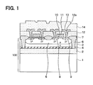
- FIG. 1 is a cross-sectional view of a SOI structure semiconductor device according to the present embodiment.
- the SOI structure semiconductor device of the present embodiment is described with reference to this figure.
- a SOI substrate 100 is formed as shown in FIG. 1 .
- a buried insulation layer 2 made of silicon dioxide film and having a thickness of from 0.1 ⁇ m to several ⁇ m is formed on a monocrystal silicon substrate 1 as a supporting substrate.
- a n-type active layer 3 made of monocrystal silicon and having a thickness of from 1 ⁇ m to several ⁇ m is formed on the buried insulation layer 2.
- a lattice distortion layer 4 as a gettering site is formed in the active layer 3.
- the lattice distortion layer 4 is formed by lattice distortion in silicon of the active layer 3.
- the lattice distortion layer 4 is described in detail later.
- a p-type well layer (impurity diffusion layer) 5 having a different conductivity than the active layer 3 is formed in a surface portion of the active layer 3.
- a trench isolation structure 6 and a LOCOS oxide film 7 are located around the p-type well layer 5 to isolate devices from each other.
- An n + -type source region 8 and an n + -type drain region 9 are formed in a surface portion of the isolated p-type well layer 5 in such a manner that they are spaced from each other.
- the surface portion of the p-type well layer 5 between the n + -type source region 8 and the n + -type drain region 9 is defined as a channel region, and a gate oxide film 10 is formed on the channel region.
- a gate electrode 11 made of doped poly-Si is formed on the gate oxide film 10.
- An interlayer insulation film 12 is formed to cover the gate electrode 11 and the gate oxide film 10.
- a contact hole 12a is formed to penetrate the interlayer insulation film 12 and the gate oxide film 10.
- a wire 13 is connected to the n + -type source region 8 and the n + -type drain region 9 through the contact hole 12a, separately.
- a passivation film 14 is formed to cover the wire 13 and the interlayer insulation film 12. In this way, in the SOI structure semiconductor device, a MOSFET is formed in the SOI substrate 100 having PN junction.
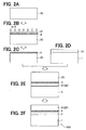
- FIGS. 2A-2F are cross-sectional views illustrating processes of making the SOI substrate 100.
- FIGS. 3A-3E are cross-sectional views illustrating processes of making the SOI structure semiconductor device shown in FIG. 1 by using the SOI substrate 100 made by the processes shown in FIG. 2 .
- a method of making the SOI structure semiconductor device is described, after a method of making the SOI substrate 100 is described.
- a monocrystal silicon substrate 20 for the active layer 3 where a device is formed is prepared.
- the silicon substrate 20 can include a n-type CZ silicon substrate (dopant: phosphorus) having a crystal plane orientation ⁇ 100> and having a resistivity of from 1 ⁇ cm to 50 ⁇ cm.
- the lattice distortion layer 4 serving as a gettering site is formed at a predetermined depth in the silicon substrate 20.
- a thermally oxidized film 21 is formed on a surface of the silicon substrate 20 by thermal oxidation, and then ion implantation of Ar ions is performed by application of a voltage of 200keV or less (e.g., 100keV).
- the amount of Ar ions to be implanted is equal to or greater than 5x10 12 /m 2 and less than 3x10 14 /cm 2 (e.g., 1x10 14 atoms/cm 2 ).
- the lattice distortion layer 4 of the present embodiment means a region where silicon crystal lattice is distorted due to implantation of atoms, such as Ar ions, that is electrically inert in silicon.
- the thermally oxidized film 21 is removed by etching by soaking the silicon substrate 20 in dilute hydrofluoric acid solution.
- a silicon substrate 1 made of monocrystal silicon and having surface area equal to surface area of the silicon substrate 20 is prepared for a supporting substrate.
- An oxide film 22 having a thickness of from 0.1 ⁇ m to 5.0 ⁇ m, preferably, from 0.5 ⁇ m to 3.0 ⁇ m is formed on a surface of the silicon substrate 1 by thermal oxidation.
- the silicon substrate 20 with the lattice distortion layer 4 and the silicon substrate 1 with the oxide film 22 are cleaned by a SC1 cleaning solution, and then the two substrates 1, 20 are placed one on top of another in such a manner that the silicon surface on the lattice distortion layer 4 side and the oxide film 22 can be in close contact with each other. Then, the two substrates are thermally treated in oxygen or nitrogen atmosphere at a temperature of 900 to 1200 °C for 30 to 120 minutes so that the two substrates can be tightly joined together through the silicon surface and the oxide film 22. In this way, the oxide film 22 is buried between the silicon substrates 1, 20 so as to form the buried insulation layer 2.
- the surface of the silicon substrate 20 with the lattice distortion layer 4 is polished and planarized so that the silicon substrate 20 can have a thickness of 0.5 to several tens of ⁇ m, preferably 5 to 20 ⁇ m.
- the silicon substrate 20 is formed into the active layer 3.
- the SOI substrate 100 is completed.
- the SOI structure semiconductor device is made by using this SOI substrate 100.
- the oxide film 22 on the silicon substrate as a supporting substrate is formed into the buried insulation layer 2.
- the thermally oxidized film 21 on the silicon substrate 20, which is to be formed into the active layer 3 can be formed into the buried insulation layer 2.
- oxide films 22 can be formed on both silicon substrates 1, 20 and joined together to form the buried insulation layer 2.
- a thermally oxidized film 31 having a thickness of about 40 nm is formed to cover a surface of the active layer 3, and a photoresist 32 is formed on the thermally oxidized film 31.
- a photolithography process an opening is formed in the photoresist 32 at a position corresponding to the p-type well layer 5. Then, for example, boron ions are selectively implanted with a dose of 2x10 13 cm -2 at an energy of 240 keV by using the photoresist 32 as a mask.
- a thermal treatment is performed in nitrogen atmosphere, for example, at a temperature of 1150 °C for 90 minutes.
- the implanted boron ions are diffused so that the p-type well layer 5 can be formed.
- a CMOS is formed in the SOI substrate 100
- a n-type well layer is formed in the same manner as the p-type well layer 5.
- an opening is formed in the photoresist at a position corresponding to the n-type well layer in a photolithography process.
- phosphorus ions are implanted with a dose of 8x10 12 cm -2 at an energy of 500 keV by using the photoresist as a mask. Then, after a remaining portion of the photoresist is removed, a thermal treatment is performed in nitrogen atmosphere, for example, at a temperature of 1000 °C for 30 minutes. Thus, the phosphorus ions are diffused so that the n-type well layer 5 can be formed.
- a Si 3 N 4 film (not shown) having a thickness of about 150 to 200 nm is formed on the thermally oxidized film 31 by a LP-CVD method.
- a photoresist (not shown) is formed on the Si 3 N 4 film.
- an opening is formed in the photoresist at a position corresponding to a trench isolation structure 6.
- the Si 3 N 4 film and the thermally oxidized film 31 are selectively removed by dry etching. In this way, the Si 3 N 4 film and the thermally oxidized film 31 are selectively removed so that the active layer 3 can be exposed in such a manner that device-forming regions are isolated from each other.
- a trench 6a is formed by dry etching the active layer 3 using the Si 3 N 4 film as a mask. Then, as necessary, chemical dry etching is performed to remove an etching-damaged layer on a surface of the trench 6a. Then, a thermally-oxidized film having a thickness of about 100 nm is formed on a side wall and a bottom of the trench 6a. Then, a CVD film is formed to fill the trench so that the trench isolation structure 6 can be formed.
- the CVD film can include a non-doped polysilicon film, a P-doped polysilicon film, a B-doped polysilicon film, an oxide film, and a nitride film. Examples of making the CVD film can include a LP-CVD, a plasma CVD, and a normal pressure CVD.
- a LOCOS oxide film 7 is formed by a so-called LOCOS oxidation method. Specifically, after a photoresist is formed, an opening is formed in the photoresist at a position corresponding to the LOCOS oxide film 7 by a photolithography process. Then, the Si 3 N 4 film is selectively removed by a dry etching using the photoresist as a mask, so that the thermally-oxidized film can be exposed. Then, after a remaining portion of the photoresist is removed, a thermal oxidation is performed by using the Si 3 N 4 film as a mask in water vapor atmosphere, for example, at a temperature of 1000 °C for 400 to 500 minutes. In this way, the LOCOS oxide film 7 is formed.
- the Si 3 N 4 film is removed by etching using phosphoric acid, and the thermally-oxidized film is removed by using a dilute HF.
- a thermal oxidation is performed in water vapor atmosphere, for example, at a temperature of 850°C to form a gate oxide film 10 having a predetermined thickness.
- a sacrifice oxidation can be performed before forming the gate oxide film 10.
- a thermal oxidation is performed at a temperature of 1000°C to form an oxide layer having a thickness of 40nm, and then the oxide layer is removed by using a dilute HF.
- a byproduct generated in production of the LOCOS oxide film 7 can be removed, and metal impurities, such as Fe, that are likely to be segregated into an oxide layer can be removed before the gate oxide layer is formed. Therefore, a quality of the gate oxide film 10 to be formed thereafter can be improved.
- a gate electrode 11 is formed by patterning the doped poly-Si film. Specifically, after a photoresist is formed on the doped poly-Si film, the photoresist is partially removed by a photolithography process in such a manner that the photoresist can be left at a position corresponding to the gate electrode. Then, a dry etching is performed by using the photoresist as a mask so that the doped poly-Si film can be selectively left at a position. In this way, the gate electrode 11 is formed. Further, ion implantation of impurities of a different conductivity than the well is performed by using the gate electrode 11 as a mask. Then, a thermal treatment is performed in nitrogen atmosphere so that a n + -type source region 8 and a n + -type drain region 9 can be formed. In this way, a N channel MOSFET is formed.
- a P channel MOSFET is formed in the n-type well layer in the same manner.
- the contact hole 12a is formed in the interlayer insulation film 12 by a photolithography process. Then, a metal layer is formed on the interlayer insulation film 12 and patterned into the wire 13 that is electrically connected through the contact hole 12a to the gate electrode 11, the n + -type source region 8, and the n + -type drain region 9. Then, the passivation film 14 is formed so that the SOI structure semiconductor device can be completed.
- the semiconductor device was cleaved in a thickness direction, and internal stress on a cleavage surface was evaluated by micro-Raman spectroscopy.
- the SOI substrate 100 with the lattice distortion layer 4 was thermally treated in nitrogen atmosphere at a temperature of 1150 °C for 350 minutes in the same manner as the high temperature thermal treatment performed in the device making process.
- Ni was applied to a surface of the active layer 3 with a concentration of about 5x10 12 atoms/cm 2 and diffused inside by performing a thermal treatment in nitrogen atmosphere at a temperature of 1000 °C for 1 hour.
- the oxide film on the surface of the active layer 3, the active layer 3, and the buried insulation layer (BOX (Buried Oxide) layer) 2, and a supporting substrate surface layer (within about 1 ⁇ m from an interface with the buried insulation layer 2) were gradually etched, and the distribution of the concentration of Ni in the thickness direction was measured by measuring the concentration of Ni in the solution by ICP-MS.
- each of the surface oxide layer and the buried insulation layer 2 was measured in one stage using a HF solution
- the active layer 3 was measured using a mixed acid solution by dividing the active layer 3 in five stages at about 1 ⁇ m interval
- the supporting substrate surface layer was measured in one stage using a mixed acid solution.
- junction leakage current of the semiconductor device was conducted as follows.
- the n-type silicon substrate 1 was grounded.
- a reverse voltage is applied between the silicon substrate 20 and the p-type well layer 5 by applying a negative voltage to the p-type well layer 5.
- the leakage current was evaluated under a condition where a voltage of the p-type well layer 5 is minus 40 V so that at depletion layer in the active layer 3 can surely extend to the lattice distortion layer 4.
- FIG. 5 is a graph illustrating a relationship between the gettering capability of the lattice distortion layer 4 and the internal stress under a condition where the thickness of the active layer 3 is 5 ⁇ m, and the thickness of the buried insulation layer 2 is 0.5 ⁇ m.
- a longitudinal axis represents a Ni capturing ratio that is defined as a ratio of the total amount of Ni impurities (the sum of the concentration of Ni in a region from the oxide film on the surface of the active layer 3 to the surface layer of the silicon substrate 1 as a supporting substrate) within with respect to the concentration of Ni in the lattice distortion layer 4 (a region within about 2 ⁇ m from the surface of the active layer 3 on the buried insulation layer 2 side). It can be seen from this figure that a sufficient gettering capability can be obtained when tensile stress is 11MPa or more.
- FIG. 6 is a graph illustrating a relationship between the junction leakage current in the lattice distortion layer 4 and the internal stress under a condition where the thickness of the active layer 3 is 5 ⁇ m, and the thickness of the buried insulation layer 2 is 0.5 ⁇ m. It can be seen from this figure that the leakage current occurs when tensile stress exceeds 27MPa or more. It can be considered that the leakage current is due to a stress-induced defect that is induced by occurrence of large tensile stress. Therefore, reducing the tensile stress to 27MPa or less can prevent the leakage current due to the stress-induced defect.
- FIGS. 5 , 6 are based on the conditions that the thickness of the active layer 3 is 5 ⁇ m and that the thickness of the buried insulation layer 2 is 0.5 ⁇ m. Therefore, if these thicknesses are changed, the lower limit of the tensile stress for the gettering capability and the upper limit of the tensile stress effective for prevention of the leakage current due to the stress-induced defect are changed.
- FIG. 7 is a graph illustrating a relationship between the internal stress and the thickness (BOX thickness) of the buried insulation layer 2 under a condition that the thickness (SOI thickness) of the active layer 3 is 5 ⁇ m or 15 ⁇ m. A positive value (+) of the internal stress represents compressive stress, and a negative value (-) of the internal stress represents tensile stress.
- the gettering capability can be surely obtained by setting the lower limit of the tensile stress in the lattice distortion layer 4 equal to or greater than the internal stress defined by the above expression. That is, the gettering capability can be surely obtained by satisfying the following second expression.
- the internal stress is expressed as an absolute value, because the tensile stress is represented as a negative value (-) of the internal stress.
- the third expression is derived from the second expression by taking into consideration a difference between the lower limit of 11MPa and the upper limit of 27MPa when the thickness of the active layer 3 is 5 ⁇ m, and the thickness of the buried insulation layer 2 is 0.5 ⁇ m.
- FIGS. 8A-8D are diagrams illustrating a result of the study.
- FIG. 8A is a graph illustrating a relationship between the dose amount of Ar ions and the leakage current in the PN junction.
- FIGS. 8B-8D illustrate relationships between the dose amount of Ar ions and the size of the crystal defect in the lattice distortion layer 4.
- occurrence of the leakage current can be prevented when the diameter of the crystal defect is less than a diameter causing dislocation, for example, 15nm.
- FIGS. 9A-9E show the relationship observed when the dose amount is 5x10 12 cm -2 , 3x10 13 cm -2 , 1x10 14 cm -2 , and 3x10 14 cm -2 , respectively.
- the emission intensity (hereinafter called the "D1 line peak intensity) at the D1 line is small and does not peak.
- the D1 line peak intensity becomes large. This means that dislocation occurred as a result of the increase in the dose amount of Ar ions.
- the dose amount of the Ar ions needs to be adjusted to satisfy this.
- the D1 line peak intensity a ratio of the D1 line peak intensity to the emission intensity (hereinafter called the "TO line peak intensity) at the TO line is calculated so that the D1 line peak value can be a relative value.
- this ratio is equal to or less than 1/3, the effect of dislocation is small enough to reduce the leakage current. Therefore, the leakage current can be reduced by adjusting the dose amount of Ar ions in such a manner that this ratio is equal to or less than 1/3.
- the leakage current occurs due to not only dislocation but also an unbonded silicon atom in a silicon lattice.
- the Gcenter line corresponds to the wavelength at which emission occurs due an unbonded silicon atom in a silicon lattice. Therefore, the leakage current can be more reduced by adjusting the emission intensity (hereinafter called the "Gcenter line peak intensity) at the Gcenter line in such a manner that the Gcenter line peak intensity is smaller than a given value.
- the Gcenter line peak intensity varies depending on measuring conditions, whether or not the Gcenter line peak intensity will affect the leakage current cannot be determined by just taking into consideration the Gcenter line peak intensity. Therefore, a ratio of the Gcenter line peak intensity to the. TO line peak intensity is calculated so that the Gcenter line peak intensity can be a relative value. In such an approach, it was confirmed that when this ratio is equal to or less than 5/7, the effect of dislocation is small enough to reduce the leakage current. Therefore, the leakage current can be reduced by adjusting the dose amount of Ar ions in such a manner that this ratio is equal to or less than 5/7.
- a junction leakage current in the SOI structure semiconductor device was measured when a depletion layer at a PN junction reached the lattice distortion layer 4 serving as a gettering site. As a result, it was confirmed that the leakage current is smaller than 1x10 -8 A/mm 2 and sometimes smaller than 3x10 -9 A/mm 2 .
- the lattice distortion layer 4 is formed by implanting Ar ions into a silicon substrate that is formed into the active layer 3.
- the lattice distortion layer 4 can serve as a gettering site.
- the dose amount of Ar ions is adjusted so that tensile stress at the lattice distortion layer 4 can be equal to or greater than 11MPa and equal to or less than 27Mpa. Therefore, the leakage current can be reduced while allowing the lattice distortion layer 4 to serve as a gettering site.
- the crystal defect in the lattice distortion layer 4 is sized not to cause dislocation.
- the dose amount of Ar ions can be adjusted so that the average diameter of the crystal defect can be 15nm or less.
- the dose amount of Ar ions can be adjusted by using cathodoluminescence method so that the ratio of the D1 line peak intensity to the TO line peak intensity is 1/3 or less, more preferably, the ratio of the D1 line peak intensity to the Gcenter line peak intensity is 5/7 or less.
- a second embodiment of the present invention is described.
- a difference between the first and second embodiments is in that an impurity diffusion region is formed in addition to the p-type well layer 5.
- FIG. 10 is a cross-sectional view of a SOI structure semiconductor device according to the present embodiment.
- an impurity diffusion region 40 is formed in a non device-forming region around the device-forming region.
- p-type impurities are implanted and diffused in the impurity diffusion region 40.
- boron is used as p-type impurities to from the impurity diffusion region 40.
- the impurity diffusion region 40 in the non device-forming region can perform gettering of metal impurities, such as Fe, that are likely to be segregated into the boron diffusion region. Therefore, even when the lattice distortion layer 4 cannot perform gettering of all Fe impurities, the impurity diffusion region 40 can prevent Fe from being concentrated into the p-type well layer 5. Thus, the quality of the gate oxide film 10 on the p-type well layer 5 can be improved, and the junction leakage can be reduced.
- the impurity diffusion region 40 can be formed by performing ion implantation and thermal diffusion of boron as p-type impurities after patterning a photoresist in a typical photolithography process.
- a manufacturing process can be simplified by forming the impurity diffusion region 40 at the same time as the p-type well layer 5.
- the photoresist is patterned in the process shown in FIG. 3A , an opening is formed in the photoresist at a position corresponding to the impurity diffusion region 40.
- ion implantation of boron is performed by using the photoresist as a mask so that bottom ions can be implanted into not only the position corresponding to the impurity diffusion region 40 but also the position corresponding to p-type well layer 5.
- the impurity diffusion region 40 can be formed at the same time as the p-type well layer 5.
- the p-type well layer 5 and the impurity diffusion region 40 can be formed in different processes.
- the dose amount of boron can be adjusted in such a manner that an impurity concentration of the impurity diffusion region 40 can be greater than an impurity concentration of the p-type well layer 5.
- the dose amount of boron can be adjusted so that the impurity concentration of boron in the impurity diffusion region can be 1x10 18 cm -3 or more. In such an approach, the effect of gettering of metal impurities that are likely to be segregated into the boron diffusion region can be improved.
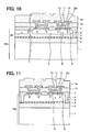
- a third embodiment of the present invention is described. A difference between the first and third embodiments is in that the p-type well layer 5 is removed.
- FIG. 11 is a cross-sectional view of a SOI structure semiconductor device according to the present embodiment.
- the active layer 3 is made of p-type monocrystalline silicon.
- the n + -type source region 8 and the n + -type drain region 9 are directly formed in the active layer 3.
- the active layer 3 forms a PN junction with the n + -type source region 8 and the n + -type drain region 9.
- a MOSFET with a PN junction is formed in the SOI structure semiconductor device.
- the same advantage as the first embodiment can be obtained by forming the lattice distortion layer 4 serving as a gettering site.
- a fourth embodiment of the present invention is described.
- a difference between the first and fourth embodiments is in that the p-type well layer 5 is removed and the active layer 3 is thinned to provide a thin SOI structure.
- FIG. 12 is a cross-sectional view of a SOI structure semiconductor device according to the present embodiment.
- the active layer 3 is made of p-type monocrystalline silicon.
- the trench isolation structure 6 provides isolation of each device.
- the n + -type source region 8 and the n + -type drain region 9 are directly formed in the active layer 3.
- the active layer 3 forms a PN junction with the n + -type source region 8 and the n + -type drain region 9.
- a MOSFET with a PN junction is formed in the SOI structure semiconductor device.
- an electric field relieving layer 8a is located closer to a channel region than the n + -type source region 8 and in contact with the n + -type source region 8
- an electric field relieving layer 9a is located closer to the channel region than the n + -type drain region 9 and in contact with the n + -type drain region 9.
- a side wall of the gate electrode 11 is covered with a side wall 15 that is made of an insulation film such as an oxide film.
- Silicide films 8b, 9b, and 11a isolated by the side wall 15 are formed on surfaces of the n + -type source region 8, the n + -type drain region 9, and the gate electrode 11, so that a salicide structure can be formed.
- n + -type source region 8 and the n + -type drain region 9 are electrically connected to each wire 13 via the silicide films 8b, 9b.
- the gate electrode 11 is electrically connected to a wire, which is not shown in the figure, via the silicide film 11a.
- the same advantage as the first embodiment can be obtained by forming the lattice distortion layer 4 serving as a gettering site.
- the manufacturing processes shown in FIGS. 2A-2F are described as an example of the manufacturing method of the SOI substrate 100.
- the SOI substrate 100 can be manufactured by any conventional method (for example, a method disclosed in JP-2000-332021A ).
- a semiconductor device having a MOSFET is described as an example of the SOI structure semiconductor device with the p-type well layer 5.
- the SOI structure semiconductor device can have a device other than a MOSFET.
- the SOI structure semiconductor device can have a bipolar transistor.
- the buried insulation layer 2 is formed with the thermally oxidized film 22.
- the buried insulation layer 2 can be formed with a film other than the thermally oxidized film 22.
- the buried insulation layer 2 can be formed with a CVD film, a nitride film, or an ONO film.
- a n-type is defined as a first conductivity type
- a p-type is defined as a second conductivity type
- a n-type can be defined as a second conductivity type
- a p-type can be defined as a first conductivity type
- tensile stress is described as an example of internal stress occurring in the lattice distortion layer 4.
- the above-described expressions and the upper and lower limits of the internal stress can be applied to when the internal stress is compressive stress.
Landscapes
- Thin Film Transistor (AREA)
- Element Separation (AREA)
- Weting (AREA)
- Metal-Oxide And Bipolar Metal-Oxide Semiconductor Integrated Circuits (AREA)
Abstract
Description
- This application is based on and incorporates herein by reference Japanese Patent Application No.
2007-273813 filed on October 22, 2007 2008-261781 - The present invention relates to a SOI structure semiconductor device formed by using a SOI substrate having a SOI layer (active layer) disposed through a silicon oxide film on a surface of a silicon substrate as a supporting substrate, and relates to a method of manufacturing the same.
- For example, Japanese Patent No.
3484961 H2-260428 2908150 - Japanese patent No.
3484961 - In Japanese Patent Application Publication No.
H2-260428 2908150 - However, the method disclosed in Japanese patent No.
3484961 - Further, according to the methods disclosed in Japanese Patent Application Publication No.
H2-260428 2908150 - In view of the above, it is an object of the present invention to provide a SOI structure semiconductor device for effectively performing gettering, for reducing a leakage current, and for preventing variations in device characteristics. It is an object of the present invention to provide a method of manufacturing the SOI structure semiconductor device.
- In order to achieve the above object, according to the present invention, a SOI structure semiconductor device includes a SOI substrate (100) having a silicon substrate (1) of monocrystalline silicon, a first conductivity type active layer (3) of monocrystalline silicon, and a buried insulation layer (2) between the silicon substrate (1) and the active layer (3). A second conductivity type layer (5, 8, 9) are located in a surface portion of the active layer (3) to form a PN junction with the active layer (3). A silicon crystalline lattice of the active layer (3) is distorted to form a lattice distortion layer (4) serving as a gettering site.
- In this way, the SOI structure semiconductor device is formed by using the SOI substrate (100), and the lattice distortion layer (4) is formed in the active layer (3). Thus, the lattice distortion layer (4) can effectively serve as a gettering site.
- For example, when a thickness of the active layer (3) is defined as X [µm], and a thickness of the buried insulation layer (2) is defined as Y [µm], a lower limit of an internal stress in the lattice distortion layer (4) can be determined to satisfy the following expression:

In such an approach, the lattice distortion layer (4) can effectively serve as a gettering site. - Preferably, when a thickness of the active layer (3) is defined as X [µm], and a thickness of the buried insulation layer (2) is defined as Y [µm], an upper limit of an internal stress in the lattice distortion layer (4) can be determined to satisfy the following expression:

In such an approach, a leakage current due to a defect induced by stress can be prevented. The internal stress is expressed as an absolute value, because tensile stress is expressed as a negative (-) value of the internal stress, and compressive stress is expressed as a positive (+) value of the internal stress. - For example, when a thickness of the active layer (3) is 5µm, and a thickness of the buried insulation layer is 0.5µm, the internal stress in the lattice distortion layer (4) can be equal to or greater than 11MPa.
- Further, when a thickness of the active layer (3) is 5µm, and a thickness of the buried insulation layer is 0.5µm, the internal stress in the lattice distortion layer (4) can be equal to or less than 27MPa.
- When the lattice distortion layer (4) is analyzed by a cathodoluminescence technique, a peak value of an emission intensity at a wavelength λ of 1535nm is defined as a D1 line peak intensity, and the peak value of the emission intensity at the wavelength λ of 1130nm is defined as a T0 line peak intensity. In this case, it is preferable that a ratio of the D1 line peak intensity to the T0 line peak intensity should be equal to or less than 1/3. For example, the ratio of the D1 line peak intensity to the T0 line peak intensity can be 1/3 by adjusting the dose amount of Ar ions when the lattice distortion layer (4) is formed. In such an approach, stress occurring in the lattice distortion layer (4) is adjusted so that a leakage current can be reduced.
- When the lattice distortion layer (4) is analyzed by a cathodoluminescence technique, a peak value of an emission intensity at a wavelength λ of 1279nm is defined as a Gcenter line peak intensity, and the peak value of the emission intensity at the wavelength λ of 1130nm is defined as a T0 line peak intensity. In this case, a ratio of the D1 line peak intensity to the T0 line peak intensity can be equal to or less than 5/7. In such an approach, the leakage current can be reduced.
- Further, an average diameter of a crystal defect in the lattice distortion layer (4) can be equal to or less than 15nm. In such an approach, occurrence of the leakage current can be prevented, because it can be considered that dislocation does not occur when the average diameter of the crystal defect is equal to or less than 15nm. Preferably, the average diameter of the crystal defect in the lattice distortion layer (4) should be greater than 0nm and equal to or less than 15nm.
- Further, in a case where a second conductivity type well layer (5) is formed in a device-forming region of the active layer (3), it is preferable that an impurity diffusion region (40) where boron is diffused is formed in a non-device forming region of the active layer (3) in addition to the lattice distortion layer (4). In such an approach, gettering of metal impurities that are likely to be segregated into the boron diffusion region can be performed. Therefore, even when the lattice distortion layer cannot perform gettering of all Fe impurities, the impurity diffusion region (40) can prevent Fe from being concentrated into the well layer (5) of p-type. Thus, the quality of the gate oxide film on the well layer (5) can be improved, and a junction leakage current between the active layer (3) and the well layer (5) can be reduced.
- In this case, if the well layer (5) is of p-type, it is preferable that a p-type impurity concentration of the impurity diffusion region (40) should be greater than that of the well layer (5). In such an approach, the effect of gettering of metal impurities that are likely to be segregated into the boron diffusion region can be improved. For example, it is preferable that a boron impurity concentration of the impurity diffusion region (40) should be equal to or greater than 1x1018cm-3.
- Further, a method of manufacturing the above SOI structure semiconductor device can include a step of performing a sacrifice oxidation before forming a gate oxide film. In the sacrifice oxidation, an oxide film is formed by thermal oxidation and then removed by using a dilute HF. A byproduct generated in production of a LOCOS oxidation film can be removed by performing such a sacrifice oxidation. Further, metal impurities, such as Fe, that are likely to be segregated into an oxide layer can be removed before the gate oxide layer is formed. Therefore, a quality of the gate oxide film (10) to be formed thereafter can be improved.
- The symbol in parentheses of each means described above corresponds to a specific means described in embodiments described later.
- The above and other objectives, features and advantages of the present invention will become more apparent from the following detailed description made with check to the accompanying drawings. In the drawings:
-
FIG. 1 is a cross-sectional view of a SOI structure semiconductor device according to a first embodiment of the present invention; -
FIGS. 2A-2F are cross--sectional views illustrating processes of manufacturing aSOI substrate 100 used for the SOI structure semiconductor device shown inFIG. 1 ; -
FIGS. 3A-3E are cross-sectional views illustrating processes of manufacturing the SOI structure semiconductor device shown inFIG. 1 by using theSOI substrate 100 manufactured by the processes shown inFIGS. 2A-2F ; -
FIG. 4 is a graph illustrating a relationship between an internal stress in alattice distortion layer 4 and the dose amount of implanted ions and a type of the implanted ions; -
FIG. 5 is a graph illustrating a relationship between the internal stress and a guttering capability of thelattice distortion layer 4; -
FIG. 6 is a graph illustrating a relationship between the internal stress and a thickness (BOX thickness) of a buriedinsulation layer 2 under a condition that a thickness (SOI thickness) of anactive layer 3 is 5µm or 151µm; -
FIG. 7 is a graph illustrating a relationship between a junction leakage current in thelattice distortion layer 4 and the internal stress; -
FIG. 8A is a graph illustrating a relationship between the dose amount of Ar ions and the leakage current in a PN junction, andFIGS. 8B-8D are diagrams illustrating relationships between the dose amount of Ar ions and the size of a crystal defect in thelattice distortion layer 4; -
FIGS. 9A-9E are diagrams illustrating a result of a cathodoluminescence analysis conducted to measure a relationship between a wavelength λ and an emission intensity by changing the dose amount of Ar ions; -
FIG. 10 is a cross-sectional view of a SOI structure semiconductor device according to a second embodiment of the present invention; -
FIG. 11 is a cross-sectional view of a SOI structure semiconductor device according to a third embodiment of the present invention; and -
FIG. 12 is a cross-sectional view of a SOI structure semiconductor device according to a fourth embodiment of the present invention. - An embodiment of the present invention is described below with reference to the drawings. In the drawings, the same symbols designate the same or corresponding portions.
- A first embodiment of the present invention is described.
FIG. 1 is a cross-sectional view of a SOI structure semiconductor device according to the present embodiment. The SOI structure semiconductor device of the present embodiment is described with reference to this figure. - A
SOI substrate 100 is formed as shown inFIG. 1 . A buriedinsulation layer 2 made of silicon dioxide film and having a thickness of from 0.1 µm to several µm is formed on amonocrystal silicon substrate 1 as a supporting substrate. A n-typeactive layer 3 made of monocrystal silicon and having a thickness of from 1µm to several µm is formed on the buriedinsulation layer 2. Alattice distortion layer 4 as a gettering site is formed in theactive layer 3. Thelattice distortion layer 4 is formed by lattice distortion in silicon of theactive layer 3. Thelattice distortion layer 4 is described in detail later. - A p-type well layer (impurity diffusion layer) 5 having a different conductivity than the
active layer 3 is formed in a surface portion of theactive layer 3. The.n-typeactive layer 3 and the p-type well layer 5 form a PN junction. - A
trench isolation structure 6 and aLOCOS oxide film 7 are located around the p-type well layer 5 to isolate devices from each other. An n+-type source region 8 and an n+-type drain region 9 are formed in a surface portion of the isolated p-type well layer 5 in such a manner that they are spaced from each other. - The surface portion of the p-
type well layer 5 between the n+-type source region 8 and the n+-type drain region 9 is defined as a channel region, and agate oxide film 10 is formed on the channel region. Agate electrode 11 made of doped poly-Si is formed on thegate oxide film 10. Aninterlayer insulation film 12 is formed to cover thegate electrode 11 and thegate oxide film 10. Acontact hole 12a is formed to penetrate theinterlayer insulation film 12 and thegate oxide film 10. Awire 13 is connected to the n+-type source region 8 and the n+-type drain region 9 through thecontact hole 12a, separately. Apassivation film 14 is formed to cover thewire 13 and theinterlayer insulation film 12. In this way, in the SOI structure semiconductor device, a MOSFET is formed in theSOI substrate 100 having PN junction. - Next, a method of making the SOI structure semiconductor device according to the present embodiment is described.
FIGS. 2A-2F are cross-sectional views illustrating processes of making theSOI substrate 100.FIGS. 3A-3E are cross-sectional views illustrating processes of making the SOI structure semiconductor device shown inFIG. 1 by using theSOI substrate 100 made by the processes shown inFIG. 2 . Below, with reference to these figures, a method of making the SOI structure semiconductor device is described, after a method of making theSOI substrate 100 is described. - Firstly, the method of making the
SOI substrate 100 is described. - A
monocrystal silicon substrate 20 for theactive layer 3 where a device is formed is prepared. Examples of thesilicon substrate 20 can include a n-type CZ silicon substrate (dopant: phosphorus) having a crystal plane orientation <100> and having a resistivity of from 1 Ωcm to 50 Ωcm. - The
lattice distortion layer 4 serving as a gettering site is formed at a predetermined depth in thesilicon substrate 20. For example, a thermally oxidizedfilm 21 is formed on a surface of thesilicon substrate 20 by thermal oxidation, and then ion implantation of Ar ions is performed by application of a voltage of 200keV or less (e.g., 100keV). For example, the amount of Ar ions to be implanted is equal to or greater than 5x10¹²/m2 and less than 3x10¹⁴/cm2 (e.g., 1x10¹⁴atoms/cm2). - Distortion occurs in silicon crystal lattice due to damage by the Ar ion implantation so that the
lattice distortion layer 4 can be formed. As shown inFIG. 4 , the internal stress in thelattice distortion layer 4 varies depending on the dose amount and the type of an element for ion implantation. Therefore, the internal stress can be adjusted within a suitable range. Specifically, an neutral element that is electrically inert in silicon is used for ion implantation in order to avoid effect on characteristics of a device formed in theactive layer 3. For example, besides Ar, any one of or a combination of the following elements can be used for ion implantation: He, Ne, Kr, Xe, C, O, Si. In summary, thelattice distortion layer 4 of the present embodiment means a region where silicon crystal lattice is distorted due to implantation of atoms, such as Ar ions, that is electrically inert in silicon. - The thermally oxidized
film 21 is removed by etching by soaking thesilicon substrate 20 in dilute hydrofluoric acid solution. - A
silicon substrate 1 made of monocrystal silicon and having surface area equal to surface area of thesilicon substrate 20 is prepared for a supporting substrate. Anoxide film 22 having a thickness of from 0.1µm to 5.0µm, preferably, from 0.5µm to 3.0µm is formed on a surface of thesilicon substrate 1 by thermal oxidation. - The
silicon substrate 20 with thelattice distortion layer 4 and thesilicon substrate 1 with theoxide film 22 are cleaned by a SC1 cleaning solution, and then the twosubstrates lattice distortion layer 4 side and theoxide film 22 can be in close contact with each other. Then, the two substrates are thermally treated in oxygen or nitrogen atmosphere at a temperature of 900 to 1200 °C for 30 to 120 minutes so that the two substrates can be tightly joined together through the silicon surface and theoxide film 22. In this way, theoxide film 22 is buried between thesilicon substrates insulation layer 2. - The surface of the
silicon substrate 20 with thelattice distortion layer 4 is polished and planarized so that thesilicon substrate 20 can have a thickness of 0.5 to several tens of µm, preferably 5 to 20 µm. Thus, thesilicon substrate 20 is formed into theactive layer 3. In this way, theSOI substrate 100 is completed. Then, the SOI structure semiconductor device is made by using thisSOI substrate 100. As described above, according to the present embodiment, theoxide film 22 on the silicon substrate as a supporting substrate is formed into the buriedinsulation layer 2. Alternatively, the thermally oxidizedfilm 21 on thesilicon substrate 20, which is to be formed into theactive layer 3, can be formed into the buriedinsulation layer 2. Alternatively,oxide films 22 can be formed on bothsilicon substrates insulation layer 2. - Next, the method of making the SOI structure semiconductor device is described with reference to
FIGS. 3A-3E . - A thermally oxidized
film 31 having a thickness of about 40 nm is formed to cover a surface of theactive layer 3, and aphotoresist 32 is formed on the thermally oxidizedfilm 31. In a photolithography process, an opening is formed in thephotoresist 32 at a position corresponding to the p-type well layer 5. Then, for example, boron ions are selectively implanted with a dose of 2x1013 cm-2 at an energy of 240 keV by using thephotoresist 32 as a mask. - After a remaining portion of the
photoresist 32 is removed, a thermal treatment is performed in nitrogen atmosphere, for example, at a temperature of 1150 °C for 90 minutes. Thus, the implanted boron ions are diffused so that the p-type well layer 5 can be formed. Although not shown in the drawings, if a CMOS is formed in theSOI substrate 100, a n-type well layer is formed in the same manner as the p-type well layer 5. For example, after a photoresist (not shown) is formed, an opening is formed in the photoresist at a position corresponding to the n-type well layer in a photolithography process. Then, for example, phosphorus ions are implanted with a dose of 8x1012 cm-2 at an energy of 500 keV by using the photoresist as a mask. Then, after a remaining portion of the photoresist is removed, a thermal treatment is performed in nitrogen atmosphere, for example, at a temperature of 1000 °C for 30 minutes. Thus, the phosphorus ions are diffused so that the n-type well layer 5 can be formed. - A Si3N4 film (not shown) having a thickness of about 150 to 200 nm is formed on the thermally oxidized
film 31 by a LP-CVD method. A photoresist (not shown) is formed on the Si3N4 film. Then, in a photolithography process, an opening is formed in the photoresist at a position corresponding to atrench isolation structure 6. Then, by using the photoresist, the Si3N4 film and the thermally oxidizedfilm 31 are selectively removed by dry etching. In this way, the Si3N4 film and the thermally oxidizedfilm 31 are selectively removed so that theactive layer 3 can be exposed in such a manner that device-forming regions are isolated from each other. - Then, a
trench 6a is formed by dry etching theactive layer 3 using the Si3N4 film as a mask. Then, as necessary, chemical dry etching is performed to remove an etching-damaged layer on a surface of thetrench 6a. Then, a thermally-oxidized film having a thickness of about 100 nm is formed on a side wall and a bottom of thetrench 6a. Then, a CVD film is formed to fill the trench so that thetrench isolation structure 6 can be formed. Examples of the CVD film can include a non-doped polysilicon film, a P-doped polysilicon film, a B-doped polysilicon film, an oxide film, and a nitride film. Examples of making the CVD film can include a LP-CVD, a plasma CVD, and a normal pressure CVD. - Then, a
LOCOS oxide film 7 is formed by a so-called LOCOS oxidation method. Specifically, after a photoresist is formed, an opening is formed in the photoresist at a position corresponding to theLOCOS oxide film 7 by a photolithography process. Then, the Si3N4 film is selectively removed by a dry etching using the photoresist as a mask, so that the thermally-oxidized film can be exposed. Then, after a remaining portion of the photoresist is removed, a thermal oxidation is performed by using the Si3N4 film as a mask in water vapor atmosphere, for example, at a temperature of 1000 °C for 400 to 500 minutes. In this way, theLOCOS oxide film 7 is formed. - Then, the Si3N4 film is removed by etching using phosphoric acid, and the thermally-oxidized film is removed by using a dilute HF. Then, a thermal oxidation is performed in water vapor atmosphere, for example, at a temperature of 850°C to form a
gate oxide film 10 having a predetermined thickness. In this case, a sacrifice oxidation can be performed before forming thegate oxide film 10. In the sacrifice oxidation, for example, a thermal oxidation is performed at a temperature of 1000°C to form an oxide layer having a thickness of 40nm, and then the oxide layer is removed by using a dilute HF. A byproduct generated in production of theLOCOS oxide film 7 can be removed, and metal impurities, such as Fe, that are likely to be segregated into an oxide layer can be removed before the gate oxide layer is formed. Therefore, a quality of thegate oxide film 10 to be formed thereafter can be improved. - After a doped poly-Si film is formed, a
gate electrode 11 is formed by patterning the doped poly-Si film. Specifically, after a photoresist is formed on the doped poly-Si film, the photoresist is partially removed by a photolithography process in such a manner that the photoresist can be left at a position corresponding to the gate electrode. Then, a dry etching is performed by using the photoresist as a mask so that the doped poly-Si film can be selectively left at a position. In this way, thegate electrode 11 is formed. Further, ion implantation of impurities of a different conductivity than the well is performed by using thegate electrode 11 as a mask. Then, a thermal treatment is performed in nitrogen atmosphere so that a n+-type source region 8 and a n+-type drain region 9 can be formed. In this way, a N channel MOSFET is formed. - Although not shown in the drawings, a P channel MOSFET is formed in the n-type well layer in the same manner.
- After the
interlayer insulation film 12 is formed on the entire substrate surface including thegate electrode 11, thecontact hole 12a is formed in theinterlayer insulation film 12 by a photolithography process. Then, a metal layer is formed on theinterlayer insulation film 12 and patterned into thewire 13 that is electrically connected through thecontact hole 12a to thegate electrode 11, the n+-type source region 8, and the n+-type drain region 9. Then, thepassivation film 14 is formed so that the SOI structure semiconductor device can be completed. - Then, an evaluation of internal stress in the SOI structure semiconductor device was conducted. Specifically, the semiconductor device was cleaved in a thickness direction, and internal stress on a cleavage surface was evaluated by micro-Raman spectroscopy.
- Further, an evaluation of gettering capability of the semiconductor device was conducted as follows. Firstly, in the process shown in
FIG. 2F , theSOI substrate 100 with thelattice distortion layer 4 was thermally treated in nitrogen atmosphere at a temperature of 1150 °C for 350 minutes in the same manner as the high temperature thermal treatment performed in the device making process. Then, Ni was applied to a surface of theactive layer 3 with a concentration of about 5x10¹² atoms/cm2 and diffused inside by performing a thermal treatment in nitrogen atmosphere at a temperature of 1000 °C for 1 hour. - Then, the oxide film on the surface of the
active layer 3, theactive layer 3, and the buried insulation layer (BOX (Buried Oxide) layer) 2, and a supporting substrate surface layer (within about 1 µm from an interface with the buried insulation layer 2) were gradually etched, and the distribution of the concentration of Ni in the thickness direction was measured by measuring the concentration of Ni in the solution by ICP-MS. Specifically, each of the surface oxide layer and the buriedinsulation layer 2 was measured in one stage using a HF solution, theactive layer 3 was measured using a mixed acid solution by dividing theactive layer 3 in five stages at about 1 µm interval, and the supporting substrate surface layer was measured in one stage using a mixed acid solution. Further, the same evaluation, except that the thermal treatment in nitrogen atmosphere at a temperature of 1150 °C for 350 minutes was performed before Ni was applied, was conducted to observe the effect of the high temperature thermal treatment, performed in the device making process, on the gettering capability. As a result, there was no difference in the gettering capability. - In addition, an evaluation of junction leakage current of the semiconductor device was conducted as follows. The n-
type silicon substrate 1 was grounded. A reverse voltage is applied between thesilicon substrate 20 and the p-type well layer 5 by applying a negative voltage to the p-type well layer 5. The leakage current was evaluated under a condition where a voltage of the p-type well layer 5 is minus 40 V so that at depletion layer in theactive layer 3 can surely extend to thelattice distortion layer 4. -
FIG. 5 is a graph illustrating a relationship between the gettering capability of thelattice distortion layer 4 and the internal stress under a condition where the thickness of theactive layer 3 is 5µm, and the thickness of the buriedinsulation layer 2 is 0.5µm. In this figure, a longitudinal axis represents a Ni capturing ratio that is defined as a ratio of the total amount of Ni impurities (the sum of the concentration of Ni in a region from the oxide film on the surface of theactive layer 3 to the surface layer of thesilicon substrate 1 as a supporting substrate) within with respect to the concentration of Ni in the lattice distortion layer 4 (a region within about 2µm from the surface of theactive layer 3 on the buriedinsulation layer 2 side). It can be seen from this figure that a sufficient gettering capability can be obtained when tensile stress is 11MPa or more. -
FIG. 6 is a graph illustrating a relationship between the junction leakage current in thelattice distortion layer 4 and the internal stress under a condition where the thickness of theactive layer 3 is 5µm, and the thickness of the buriedinsulation layer 2 is 0.5µm. It can be seen from this figure that the leakage current occurs when tensile stress exceeds 27MPa or more. It can be considered that the leakage current is due to a stress-induced defect that is induced by occurrence of large tensile stress. Therefore, reducing the tensile stress to 27MPa or less can prevent the leakage current due to the stress-induced defect. - It is noted that the graphs illustrated in
FIGS. 5 ,6 are based on the conditions that the thickness of theactive layer 3 is 5µm and that the thickness of the buriedinsulation layer 2 is 0.5µm. Therefore, if these thicknesses are changed, the lower limit of the tensile stress for the gettering capability and the upper limit of the tensile stress effective for prevention of the leakage current due to the stress-induced defect are changed.FIG. 7 is a graph illustrating a relationship between the internal stress and the thickness (BOX thickness) of the buriedinsulation layer 2 under a condition that the thickness (SOI thickness) of theactive layer 3 is 5µm or 15µm. A positive value (+) of the internal stress represents compressive stress, and a negative value (-) of the internal stress represents tensile stress. - As can be seen from this figure, even when the thickness of the
active layer 3 is kept constant, if the thickness of the buriedinsulation layer 2 varies, internal stress acting between these varies. Therefore, in order to reduce the leakage current and allow thelattice distortion layer 4 to serve as a gettering site even if the internal stress varies, there is a need to determine the lower limit of the tensile stress for thelattice distortion layer 4 by taking into consideration these internal stress. From the examination result, it was confirmed that downward-sloping graphs can be drawn, for example, when the thickness of the buriedinsulation layer 2 is 0.5µm and 1.3µm. From the graphs, the internal stress can be defined by the following first expression. In the first expression, X represents the thickness [µm] of theactive layer 3, and Y represents the thickness [µm] of the buriedinsulation layer 2.
- Therefore, the gettering capability can be surely obtained by setting the lower limit of the tensile stress in the
lattice distortion layer 4 equal to or greater than the internal stress defined by the above expression. That is, the gettering capability can be surely obtained by satisfying the following second expression. The internal stress is expressed as an absolute value, because the tensile stress is represented as a negative value (-) of the internal stress. -

The same holds true for the upper limit of the tensile stress in thelattice distortion layer 4. That is, the leakage current can be effectively prevented by satisfying the following third expression. It is noted that the third expression is derived from the second expression by taking into consideration a difference between the lower limit of 11MPa and the upper limit of 27MPa when the thickness of theactive layer 3 is 5µm, and the thickness of the buriedinsulation layer 2 is 0.5µm.
Furthermore, a relationship between crystal defect and the leakage current in a PN junction was studied as follows. The size of the crystal defect in thelattice distortion layer 4 was adjusted by changing the dose amount of Ar ions, and a relationship between the size of the crystal defect and the leakage current in the PN junction was studied.FIGS. 8A-8D are diagrams illustrating a result of the study.FIG. 8A is a graph illustrating a relationship between the dose amount of Ar ions and the leakage current in the PN junction.FIGS. 8B-8D illustrate relationships between the dose amount of Ar ions and the size of the crystal defect in thelattice distortion layer 4. - As shown in
FIG. 8A , when the dose amount of Ar ions is zero and 1x1014cm-2, the leakage current in the PN junction does not occur. However, when the dose amount of Ar ions is 3x1014cm-2 and 1x1015cm-2, the leakage current in the PN junction occurs. As shown inFIG. 8B , when the dose amount is 1x1014cm-2, the average diameter of the crystal defect is about 5nm. As shown inFIG. 8C , when the dose amount is 3x1014cm-2, the average diameter of the crystal defect is greater than 15nm. As shown inFIG. 8D , when the dose amount is 1x1015cm-2, the average diameter of the crystal defect is greater than 15nm. As shown inFIGS. 8C, 8D , when the average diameter of the crystal defect exceeds 15nm, dislocation occurs. - Therefore, it can be considered that occurrence of the leakage current can be prevented when the diameter of the crystal defect is less than a diameter causing dislocation, for example, 15nm.
- Further, in order to study a detail relationship between the dose amount of the implanted Ar ions and the crystal defect, a relationship between a wavelength λ and emission intensity was measured by cathodoluminescence (CL) analysis while changing the dose amount of Ar ions. This relationship is shown in
FIGS. 9A-9E . -
FIGS. 9A-9E show the relationship observed when the dose amount is 5x1012cm-2, 3x1013cm-2, 1x1014cm-2, and 3x1014cm-2, respectively. In the figures, a D1 line (λ = 1535 nm) corresponds to a wavelength at which emission occurs due to dislocation, a TO line corresponds to a wavelength (λ = 1130 nm) at which emission occurs due to a typical silicon atom forming Si-Si bonds, and a Gcenter line corresponds to a wavelength (λ = 1279 nm) at which emission occurs due an unbonded silicon atom in a silicon lattice. - As can be seen from
FIGS. 9A-9E , when the dose amount of Ar ions is small, the emission intensity (hereinafter called the "D1 line peak intensity) at the D1 line is small and does not peak. However, when the dose amount of Ar ions is increased to 3x1014cm-2 the D1 line peak intensity becomes large. This means that dislocation occurred as a result of the increase in the dose amount of Ar ions. In other words, it can be considered that when the D1 line peak intensity is smaller than a given value, dislocation will hardly occur. Therefore, the dose amount of the Ar ions needs to be adjusted to satisfy this. - However, since the emission intensity varies depending on measuring conditions, whether or not the D1 line peak intensity will affect the leakage current cannot be determined by just taking into consideration the D1 line peak intensity. Therefore, a ratio of the D1 line peak intensity to the emission intensity (hereinafter called the "TO line peak intensity) at the TO line is calculated so that the D1 line peak value can be a relative value. In such an approach, it was confirmed that when this ratio is equal to or less than 1/3, the effect of dislocation is small enough to reduce the leakage current. Therefore, the leakage current can be reduced by adjusting the dose amount of Ar ions in such a manner that this ratio is equal to or less than 1/3.
- It is noted that the leakage current occurs due to not only dislocation but also an unbonded silicon atom in a silicon lattice. As described above, the Gcenter line corresponds to the wavelength at which emission occurs due an unbonded silicon atom in a silicon lattice. Therefore, the leakage current can be more reduced by adjusting the emission intensity (hereinafter called the "Gcenter line peak intensity) at the Gcenter line in such a manner that the Gcenter line peak intensity is smaller than a given value.
- However, since the Gcenter line peak intensity varies depending on measuring conditions, whether or not the Gcenter line peak intensity will affect the leakage current cannot be determined by just taking into consideration the Gcenter line peak intensity. Therefore, a ratio of the Gcenter line peak intensity to the. TO line peak intensity is calculated so that the Gcenter line peak intensity can be a relative value. In such an approach, it was confirmed that when this ratio is equal to or less than 5/7, the effect of dislocation is small enough to reduce the leakage current. Therefore, the leakage current can be reduced by adjusting the dose amount of Ar ions in such a manner that this ratio is equal to or less than 5/7.
- For reference, a junction leakage current in the SOI structure semiconductor device was measured when a depletion layer at a PN junction reached the
lattice distortion layer 4 serving as a gettering site. As a result, it was confirmed that the leakage current is smaller than 1x10⁻⁸A/mm2 and sometimes smaller than 3x10⁻⁹A/mm2. - As described above, according to the embodiment, the
lattice distortion layer 4 is formed by implanting Ar ions into a silicon substrate that is formed into theactive layer 3. In such an approach, thelattice distortion layer 4 can serve as a gettering site. Further, the dose amount of Ar ions is adjusted so that tensile stress at thelattice distortion layer 4 can be equal to or greater than 11MPa and equal to or less than 27Mpa. Therefore, the leakage current can be reduced while allowing thelattice distortion layer 4 to serve as a gettering site. - The crystal defect in the
lattice distortion layer 4 is sized not to cause dislocation. For example, the dose amount of Ar ions can be adjusted so that the average diameter of the crystal defect can be 15nm or less. Further, the dose amount of Ar ions can be adjusted by using cathodoluminescence method so that the ratio of the D1 line peak intensity to the TO line peak intensity is 1/3 or less, more preferably, the ratio of the D1 line peak intensity to the Gcenter line peak intensity is 5/7 or less. - A second embodiment of the present invention is described. A difference between the first and second embodiments is in that an impurity diffusion region is formed in addition to the p-
type well layer 5. -
FIG. 10 is a cross-sectional view of a SOI structure semiconductor device according to the present embodiment. As shown in this figure, animpurity diffusion region 40 is formed in a non device-forming region around the device-forming region. Like the p-type well layer 5, p-type impurities are implanted and diffused in theimpurity diffusion region 40. Specifically, boron is used as p-type impurities to from theimpurity diffusion region 40. - The
impurity diffusion region 40 in the non device-forming region can perform gettering of metal impurities, such as Fe, that are likely to be segregated into the boron diffusion region. Therefore, even when thelattice distortion layer 4 cannot perform gettering of all Fe impurities, theimpurity diffusion region 40 can prevent Fe from being concentrated into the p-type well layer 5. Thus, the quality of thegate oxide film 10 on the p-type well layer 5 can be improved, and the junction leakage can be reduced. - The
impurity diffusion region 40 can be formed by performing ion implantation and thermal diffusion of boron as p-type impurities after patterning a photoresist in a typical photolithography process. A manufacturing process can be simplified by forming theimpurity diffusion region 40 at the same time as the p-type well layer 5. In this case, when the photoresist is patterned in the process shown inFIG. 3A , an opening is formed in the photoresist at a position corresponding to theimpurity diffusion region 40. Then, ion implantation of boron is performed by using the photoresist as a mask so that bottom ions can be implanted into not only the position corresponding to theimpurity diffusion region 40 but also the position corresponding to p-type well layer 5. Then, thermal treatment is performed, for example, in nitrogen atmosphere at a temperature of 1150 °C for 90 minutes so that the boron ions can be diffused. In this way, theimpurity diffusion region 40 can be formed at the same time as the p-type well layer 5. - Alternatively, the p-
type well layer 5 and theimpurity diffusion region 40 can be formed in different processes. In this case, the dose amount of boron can be adjusted in such a manner that an impurity concentration of theimpurity diffusion region 40 can be greater than an impurity concentration of the p-type well layer 5. For example, the dose amount of boron can be adjusted so that the impurity concentration of boron in the impurity diffusion region can be 1x1018cm-3 or more. In such an approach, the effect of gettering of metal impurities that are likely to be segregated into the boron diffusion region can be improved. - A third embodiment of the present invention is described. A difference between the first and third embodiments is in that the p-
type well layer 5 is removed. -
FIG. 11 is a cross-sectional view of a SOI structure semiconductor device according to the present embodiment. As shown in this figure, theactive layer 3 is made of p-type monocrystalline silicon. The n+-type source region 8 and the n+-type drain region 9 are directly formed in theactive layer 3. In such a structure, theactive layer 3 forms a PN junction with the n+-type source region 8 and the n+-type drain region 9. Thus, a MOSFET with a PN junction is formed in the SOI structure semiconductor device. - Even in this structure, the same advantage as the first embodiment can be obtained by forming the
lattice distortion layer 4 serving as a gettering site. - A fourth embodiment of the present invention is described. A difference between the first and fourth embodiments is in that the p-
type well layer 5 is removed and theactive layer 3 is thinned to provide a thin SOI structure. -
FIG. 12 is a cross-sectional view of a SOI structure semiconductor device according to the present embodiment. As shown in this figure, theactive layer 3 is made of p-type monocrystalline silicon. Thetrench isolation structure 6 provides isolation of each device. The n+-type source region 8 and the n+-type drain region 9 are directly formed in theactive layer 3. In such a structure, theactive layer 3 forms a PN junction with the n+-type source region 8 and the n+-type drain region 9. Thus, a MOSFET with a PN junction is formed in the SOI structure semiconductor device. - Further, an electric
field relieving layer 8a is located closer to a channel region than the n+-type source region 8 and in contact with the n+-type source region 8, and an electricfield relieving layer 9a is located closer to the channel region than the n+-type drain region 9 and in contact with the n+-type drain region 9. A side wall of thegate electrode 11 is covered with aside wall 15 that is made of an insulation film such as an oxide film.Silicide films side wall 15 are formed on surfaces of the n+-type source region 8, the n+-type drain region 9, and thegate electrode 11, so that a salicide structure can be formed. The n+-type source region 8 and the n+-type drain region 9 are electrically connected to eachwire 13 via thesilicide films gate electrode 11 is electrically connected to a wire, which is not shown in the figure, via thesilicide film 11a. - Even in this structure, the same advantage as the first embodiment can be obtained by forming the
lattice distortion layer 4 serving as a gettering site. - According to the above-described embodiments, the manufacturing processes shown in
FIGS. 2A-2F are described as an example of the manufacturing method of theSOI substrate 100. Alternatively, theSOI substrate 100 can be manufactured by any conventional method (for example, a method disclosed inJP-2000-332021A - According to the above-described embodiments, a semiconductor device having a MOSFET is described as an example of the SOI structure semiconductor device with the p-
type well layer 5. Alternatively, the SOI structure semiconductor device can have a device other than a MOSFET. For example, the SOI structure semiconductor device can have a bipolar transistor. - According to the above-described embodiments, the buried
insulation layer 2 is formed with the thermally oxidizedfilm 22. Alternatively, the buriedinsulation layer 2 can be formed with a film other than the thermally oxidizedfilm 22. For example, the buriedinsulation layer 2 can be formed with a CVD film, a nitride film, or an ONO film. - According to the above-described embodiments, a n-type is defined as a first conductivity type, and a p-type is defined as a second conductivity type. Alternatively, a n-type can be defined as a second conductivity type, and a p-type can be defined as a first conductivity type.
- According to the above-described embodiments, tensile stress is described as an example of internal stress occurring in the
lattice distortion layer 4. The same holds true for when the internal force occurring in thelattice distortion layer 4 is compressive stress. The above-described expressions and the upper and lower limits of the internal stress can be applied to when the internal stress is compressive stress.
Claims (13)
- A SOI structure semiconductor device comprising:a SOI substrate (100) including a silicon substrate (1) of monocrystalline silicon, a first conductivity type active layer (3) of monocrystalline silicon, and a buried insulation layer (2) between the silicon substrate (1) and the active layer (3); anda second conductivity type layer (5, 8, 9) formed in a surface portion of the active layer (3) to form a PN junction with the active layer (3), whereina silicon crystalline lattice of the active layer (3) is distorted to form a lattice distortion layer (4) serving as a gettering site.
- The SOI structure semiconductor device according to claim 1, wherein
a thickness of the active layer (3) is defined as X [µm],
a thickness of the buried insulation layer (2) is defined as Y [µm], and
an internal stress in the lattice distortion layer (4) satisfies the followings:
- The SOI structure semiconductor device according to claim 1 or 2, wherein
a thickness of the active layer (3) is defined as X [µm],
a thickness of the buried insulation layer (2) is defined as Y [µm], and
an internal stress in the lattice distortion layer (4) satisfies the followings:
- The SOI structure semiconductor device according to claim 1, wherein
a thickness of the active layer (3) is 5µm,
a thickness of the buried insulation layer (2) is 0.5µm, and
an internal stress in the lattice distortion layer (4) is equal to or greater than 11MPa. - The SOI structure semiconductor device according to claim 1 or 4, wherein
a thickness of the active layer (3) is 5µm,
a thickness of the buried insulation layer (2) is 0.5µm, and
an internal stress in the lattice distortion layer (4) is equal to or less than 27MPa. - The SOI structure semiconductor device according to any one of claims 1-5, wherein
when the lattice distortion layer (4) is analyzed by a cathodoluminescence technique, a peak value of an emission intensity at a wavelength λ of 1535nm is defined as a D1 line peak intensity, and the peak value of the emission intensity at the wavelength λ of 1130nm is defined as a T0 line peak intensity, and
a ratio of the D1 line peak intensity to the T0 line peak intensity is equal to or less than 1/3. - The SOI structure semiconductor device according to any one of claims 1-6, wherein
when the lattice distortion layer (4) is analyzed by a cathodoluminescence technique, a peak value of an emission intensity at a wavelength λ of 1279nm is defined as a Gcenter line peak intensity, and the peak value of the emission intensity at the wavelength λ of 1130nm is defined as a T0 line peak intensity, and
a ratio of the D1 line peak intensity to the T0 line peak intensity is equal to or less than 5/7. - The SOI structure semiconductor device according to any one of claims 1-7, wherein
an average diameter of a crystal defect in the lattice distortion layer (4) is equal to or less than 15nm. - The SOI structure semiconductor device according to any one of claims 1-7, wherein
an average diameter of a crystal defect in the lattice distortion layer (4) is greater than 0nm and equal to or less than 15nm. - The SOI structure semiconductor device according to any one of claims 1-9, wherein
a second conductivity type well layer (5) is located in a device-forming region of the active layer (3), and
an impurity diffusion region (40) where boron is diffused is located in a non-device forming region of the active layer (3) in addition to the lattice distortion layer (4). - The SOI structure semiconductor device according to claim 10, wherein
when the well layer (5) is of p-type, a p-type impurity concentration of the impurity diffusion region (40) is greater than that of the well layer (5). - The SOI structure semiconductor device according to claim 10 or 11, wherein
a boron impurity concentration of the impurity diffusion region (40) is equal to or greater than 1x1018cm-3. - A method of manufacturing the SOI structure semiconductor device according to any one of claims 1-12, the method comprising:forming a gate oxide film (10) on a surface of the active layer (3);performing a sacrifice oxidation before forming the gate oxide film (10), whereinperforming the sacrifice oxidation includes forming an oxide film by thermal oxidation and removing the oxide film formed by the thermal oxidation using a dilute HF.
Priority Applications (1)
| Application Number | Priority Date | Filing Date | Title |
|---|---|---|---|
| EP14167851.6A EP2800138A1 (en) | 2007-10-22 | 2008-10-20 | SOI (silicon on insulator) structure semiconductor device and method of manufacturing the same |
Applications Claiming Priority (3)
| Application Number | Priority Date | Filing Date | Title |
|---|---|---|---|
| JP2007273813 | 2007-10-22 | ||
| JP2008261781A JP5499455B2 (en) | 2007-10-22 | 2008-10-08 | SOI (Siliconon Insulator) Structure Semiconductor Device and Method of Manufacturing the Same |
| PCT/JP2008/002964 WO2009054115A1 (en) | 2007-10-22 | 2008-10-20 | SEMICONDUCTOR DEVICE OF SOI (Silicon on insulator) STRUCTURE, AND ITS MANUFACTURING METHOD |
Related Child Applications (1)
| Application Number | Title | Priority Date | Filing Date |
|---|---|---|---|
| EP14167851.6A Division EP2800138A1 (en) | 2007-10-22 | 2008-10-20 | SOI (silicon on insulator) structure semiconductor device and method of manufacturing the same |
Publications (2)
| Publication Number | Publication Date |
|---|---|
| EP2207194A1 true EP2207194A1 (en) | 2010-07-14 |
| EP2207194A4 EP2207194A4 (en) | 2013-01-23 |
Family
ID=40579224
Family Applications (2)
| Application Number | Title | Priority Date | Filing Date |
|---|---|---|---|
| EP14167851.6A Pending EP2800138A1 (en) | 2007-10-22 | 2008-10-20 | SOI (silicon on insulator) structure semiconductor device and method of manufacturing the same |
| EP08841352A Ceased EP2207194A4 (en) | 2007-10-22 | 2008-10-20 | SOI STRUCTURE SEMICONDUCTOR DEVICE (Silicon on Insulator), AND METHOD FOR MANUFACTURING THE SAME |
Family Applications Before (1)
| Application Number | Title | Priority Date | Filing Date |
|---|---|---|---|
| EP14167851.6A Pending EP2800138A1 (en) | 2007-10-22 | 2008-10-20 | SOI (silicon on insulator) structure semiconductor device and method of manufacturing the same |
Country Status (5)
| Country | Link |
|---|---|
| US (1) | US8410573B2 (en) |
| EP (2) | EP2800138A1 (en) |
| JP (1) | JP5499455B2 (en) |
| CN (2) | CN101836281B (en) |
| WO (1) | WO2009054115A1 (en) |
Cited By (2)
| Publication number | Priority date | Publication date | Assignee | Title |
|---|---|---|---|---|
| US20130069203A1 (en) * | 2011-09-20 | 2013-03-21 | Stmicroelectronics Pte. Ltd. | Gettering method for dielectrically isolated devices |
| EP4415027A1 (en) * | 2023-02-09 | 2024-08-14 | Infineon Technologies AG | Semiconductor device and methods for fabricating a semiconductor device |
Families Citing this family (6)
| Publication number | Priority date | Publication date | Assignee | Title |
|---|---|---|---|---|
| JP2010258083A (en) * | 2009-04-22 | 2010-11-11 | Panasonic Corp | SOI wafer, method for manufacturing the same, and method for manufacturing a semiconductor device |
| US8748285B2 (en) * | 2011-11-28 | 2014-06-10 | International Business Machines Corporation | Noble gas implantation region in top silicon layer of semiconductor-on-insulator substrate |
| CN103943547B (en) * | 2013-01-23 | 2017-02-08 | 中国科学院上海微系统与信息技术研究所 | Enhanced absorption based method for preparing material-on-insulator |
| JP6098327B2 (en) * | 2013-04-18 | 2017-03-22 | 株式会社デンソー | Semiconductor device |
| US10431684B2 (en) * | 2016-04-22 | 2019-10-01 | Texas Instruments Incorporated | Method for improving transistor performance |
| US11342457B2 (en) * | 2017-09-18 | 2022-05-24 | Intel Corporation | Strained thin film transistors |
Family Cites Families (26)
| Publication number | Priority date | Publication date | Assignee | Title |
|---|---|---|---|---|
| JPH02260428A (en) | 1989-03-31 | 1990-10-23 | Hitachi Ltd | Semiconductor substrate and device |
| JP2908150B2 (en) | 1992-11-27 | 1999-06-21 | 日本電気株式会社 | SOI substrate structure and manufacturing method thereof |
| JPH0818054A (en) * | 1994-04-28 | 1996-01-19 | Nippondenso Co Ltd | Semiconductor device and its manufacture |
| JPH0878644A (en) * | 1994-09-02 | 1996-03-22 | Hitachi Ltd | Method for manufacturing semiconductor integrated circuit device |
| JP3542189B2 (en) * | 1995-03-08 | 2004-07-14 | 株式会社ルネサステクノロジ | Semiconductor device manufacturing method and semiconductor device |
| JP3612144B2 (en) * | 1996-06-04 | 2005-01-19 | 株式会社ルネサステクノロジ | Manufacturing method of semiconductor device |
| JPH1032209A (en) * | 1996-07-17 | 1998-02-03 | Hitachi Ltd | SOI wafer, method of manufacturing the same, and semiconductor integrated circuit device using the SOI wafer |
| JPH1117000A (en) * | 1997-06-27 | 1999-01-22 | Mitsubishi Electric Corp | Semiconductor device and manufacturing method thereof |
| JPH1167778A (en) * | 1997-08-19 | 1999-03-09 | Sumitomo Metal Ind Ltd | Method for manufacturing SOI semiconductor wafer |
| JP3484961B2 (en) | 1997-12-26 | 2004-01-06 | 三菱住友シリコン株式会社 | Method for manufacturing SOI substrate |
| US6255195B1 (en) | 1999-02-22 | 2001-07-03 | Intersil Corporation | Method for forming a bonded substrate containing a planar intrinsic gettering zone and substrate formed by said method |
| JP4066574B2 (en) * | 1999-03-04 | 2008-03-26 | 富士電機デバイステクノロジー株式会社 | Manufacturing method of semiconductor device |
| JP2000332021A (en) | 1999-05-18 | 2000-11-30 | Hitachi Ltd | SOI substrate and method of manufacturing the same, semiconductor device and method of manufacturing the same |
| US7119365B2 (en) * | 2002-03-26 | 2006-10-10 | Sharp Kabushiki Kaisha | Semiconductor device and manufacturing method thereof, SOI substrate and display device using the same, and manufacturing method of the SOI substrate |
| JP4115283B2 (en) * | 2003-01-07 | 2008-07-09 | シャープ株式会社 | Semiconductor device and manufacturing method thereof |
| DE102004021113B4 (en) * | 2004-04-29 | 2006-04-20 | Siltronic Ag | SOI disk and process for its production |
| JP2006073572A (en) * | 2004-08-31 | 2006-03-16 | Oki Electric Ind Co Ltd | Semiconductor crystal defect testing method and equipment thereof, and semiconductor device manufacturing method using the semiconductor crystal defect testing equipment |
| JP2006134925A (en) | 2004-11-02 | 2006-05-25 | Nec Electronics Corp | Soi substrate and its manufacturing method |
| KR100632463B1 (en) * | 2005-02-07 | 2006-10-11 | 삼성전자주식회사 | Epitaxial semiconductor substrate manufacturing method and image sensor manufacturing method, epitaxial semiconductor substrate and image sensor using same |
| JP2007095951A (en) | 2005-09-28 | 2007-04-12 | Denso Corp | Semiconductor substrate and manufacturing method thereof |
| JP2007157935A (en) | 2005-12-02 | 2007-06-21 | Denso Corp | Semiconductor device and manufacturing method thereof |
| WO2007125863A1 (en) * | 2006-04-24 | 2007-11-08 | Shin-Etsu Handotai Co., Ltd. | Soi wafer manufacturing method |
| JP5532527B2 (en) | 2006-08-03 | 2014-06-25 | 株式会社デンソー | SOI substrate and manufacturing method thereof |
| JP5248838B2 (en) * | 2007-10-25 | 2013-07-31 | 信越化学工業株式会社 | Manufacturing method of semiconductor substrate |
| JP2010245165A (en) * | 2009-04-02 | 2010-10-28 | Mitsubishi Electric Corp | Power semiconductor device manufacturing method and power semiconductor device manufacturing apparatus |
| JP6083404B2 (en) * | 2014-03-17 | 2017-02-22 | 信越半導体株式会社 | Semiconductor substrate evaluation method |
-
2008
- 2008-10-08 JP JP2008261781A patent/JP5499455B2/en not_active Expired - Fee Related
- 2008-10-20 CN CN2008801125346A patent/CN101836281B/en not_active Expired - Fee Related
- 2008-10-20 WO PCT/JP2008/002964 patent/WO2009054115A1/en not_active Ceased
- 2008-10-20 EP EP14167851.6A patent/EP2800138A1/en active Pending
- 2008-10-20 CN CN201210109975.9A patent/CN102637699B/en not_active Expired - Fee Related
- 2008-10-20 US US12/734,240 patent/US8410573B2/en not_active Expired - Fee Related
- 2008-10-20 EP EP08841352A patent/EP2207194A4/en not_active Ceased
Cited By (3)
| Publication number | Priority date | Publication date | Assignee | Title |
|---|---|---|---|---|
| US20130069203A1 (en) * | 2011-09-20 | 2013-03-21 | Stmicroelectronics Pte. Ltd. | Gettering method for dielectrically isolated devices |
| US8664746B2 (en) * | 2011-09-20 | 2014-03-04 | Stmicroelectronics Pte. Ltd. | Gettering method for dielectrically isolated devices |
| EP4415027A1 (en) * | 2023-02-09 | 2024-08-14 | Infineon Technologies AG | Semiconductor device and methods for fabricating a semiconductor device |
Also Published As
| Publication number | Publication date |
|---|---|
| CN102637699A (en) | 2012-08-15 |
| US8410573B2 (en) | 2013-04-02 |
| WO2009054115A1 (en) | 2009-04-30 |
| US20100264510A1 (en) | 2010-10-21 |
| CN102637699B (en) | 2016-01-06 |
| CN101836281A (en) | 2010-09-15 |
| EP2800138A1 (en) | 2014-11-05 |
| JP2009124116A (en) | 2009-06-04 |
| CN101836281B (en) | 2012-05-30 |
| JP5499455B2 (en) | 2014-05-21 |
| EP2207194A4 (en) | 2013-01-23 |
Similar Documents
| Publication | Publication Date | Title |
|---|---|---|
| US8410573B2 (en) | SOI (silicon on insulator) structure semiconductor device and method of manufacturing the same | |
| US6335251B2 (en) | Semiconductor apparatus having elevated source and drain structure and manufacturing method therefor | |
| US8283226B2 (en) | Method for manufacturing semiconductor device | |
| TWI446453B (en) | Field-effect transistor with stress and manufacturing method thereof | |
| US7060579B2 (en) | Increased drive current by isotropic recess etch | |
| CN102165571B (en) | Method for fabricating MOS devices with highly stressed channels | |
| US8963248B2 (en) | Semiconductor device having SSOI substrate with relaxed tensile stress | |
| US7981750B2 (en) | Methods of fabrication of channel-stressed semiconductor devices | |
| US20090283842A1 (en) | Semiconductor device and method of fabricating the same | |
| US20090166755A1 (en) | Growth of unfaceted sige along a semiconductor device width | |
| US8563382B2 (en) | Semiconductor device | |
| EP1365447A2 (en) | Manufacturing method of semiconductor substrate | |
| JP2006013082A (en) | Semiconductor device, manufacturing method thereof, and evaluation method of semiconductor device | |
| US20120205716A1 (en) | Epitaxially Grown Extension Regions for Scaled CMOS Devices | |
| US20110027954A1 (en) | Method to improve transistor tox using si recessing with no additional masking steps | |
| US20130069123A1 (en) | Cmos semiconductor devices having stressor regions and related fabrication methods | |
| CN108615731B (en) | Semiconductor device and manufacturing method thereof | |
| US7129127B2 (en) | Integration scheme to improve NMOS with poly cap while mitigating PMOS degradation | |
| US20090170270A1 (en) | Integration schemes to avoid faceted sige | |
| JP5870478B2 (en) | Manufacturing method of semiconductor device | |
| JP5200476B2 (en) | Semiconductor device and manufacturing method thereof | |
| US6737315B2 (en) | Method of manufacturing semiconductor device including steps of forming both insulating film and epitaxial semiconductor on substrate | |
| JP2007281038A (en) | Semiconductor device | |
| US20060065926A1 (en) | Insulated gate semiconductor device and manufacturing method of the same | |
| US20130240999A1 (en) | Effecting selectivity of silicon or silicon-germanium deposition on a silicon or silicon-germanium substrate by doping |
Legal Events
| Date | Code | Title | Description |
|---|---|---|---|
| PUAI | Public reference made under article 153(3) epc to a published international application that has entered the european phase |
Free format text: ORIGINAL CODE: 0009012 |
|
| 17P | Request for examination filed |
Effective date: 20100429 |
|
| AK | Designated contracting states |
Kind code of ref document: A1 Designated state(s): AT BE BG CH CY CZ DE DK EE ES FI FR GB GR HR HU IE IS IT LI LT LU LV MC MT NL NO PL PT RO SE SI SK TR |
|
| AX | Request for extension of the european patent |
Extension state: AL BA MK RS |
|
| DAX | Request for extension of the european patent (deleted) | ||
| A4 | Supplementary search report drawn up and despatched |
Effective date: 20130104 |
|
| RIC1 | Information provided on ipc code assigned before grant |
Ipc: H01L 29/32 20060101ALI20121220BHEP Ipc: H01L 21/322 20060101ALI20121220BHEP Ipc: H01L 27/12 20060101ALI20121220BHEP Ipc: H01L 21/02 20060101AFI20121220BHEP Ipc: H01L 21/84 20060101ALI20121220BHEP Ipc: H01L 21/762 20060101ALI20121220BHEP Ipc: H01L 29/786 20060101ALI20121220BHEP Ipc: H01L 21/336 20060101ALI20121220BHEP |
|
| 17Q | First examination report despatched |
Effective date: 20140103 |
|
| RAP1 | Party data changed (applicant data changed or rights of an application transferred) |
Owner name: DENSO CORPORATION Owner name: SHIN-ETSU HANDOTAI CO., LTD. |
|
| REG | Reference to a national code |
Ref country code: DE Ref legal event code: R003 |
|
| STAA | Information on the status of an ep patent application or granted ep patent |
Free format text: STATUS: THE APPLICATION HAS BEEN REFUSED |
|
| 18R | Application refused |
Effective date: 20180427 |