EP2206414B1 - A ballast circuit - Google Patents
A ballast circuit Download PDFInfo
- Publication number
- EP2206414B1 EP2206414B1 EP08845841A EP08845841A EP2206414B1 EP 2206414 B1 EP2206414 B1 EP 2206414B1 EP 08845841 A EP08845841 A EP 08845841A EP 08845841 A EP08845841 A EP 08845841A EP 2206414 B1 EP2206414 B1 EP 2206414B1
- Authority
- EP
- European Patent Office
- Prior art keywords
- lamp
- lamps
- resonance
- capacitor
- fluorescent lamps
- Prior art date
- Legal status (The legal status is an assumption and is not a legal conclusion. Google has not performed a legal analysis and makes no representation as to the accuracy of the status listed.)
- Not-in-force
Links
Images
Classifications
-
- H—ELECTRICITY
- H05—ELECTRIC TECHNIQUES NOT OTHERWISE PROVIDED FOR
- H05B—ELECTRIC HEATING; ELECTRIC LIGHT SOURCES NOT OTHERWISE PROVIDED FOR; CIRCUIT ARRANGEMENTS FOR ELECTRIC LIGHT SOURCES, IN GENERAL
- H05B41/00—Circuit arrangements or apparatus for igniting or operating discharge lamps
- H05B41/14—Circuit arrangements
- H05B41/26—Circuit arrangements in which the lamp is fed by power derived from dc by means of a converter, e.g. by high-voltage dc
- H05B41/28—Circuit arrangements in which the lamp is fed by power derived from dc by means of a converter, e.g. by high-voltage dc using static converters
- H05B41/295—Circuit arrangements in which the lamp is fed by power derived from dc by means of a converter, e.g. by high-voltage dc using static converters with semiconductor devices and specially adapted for lamps with preheating electrodes, e.g. for fluorescent lamps
- H05B41/298—Arrangements for protecting lamps or circuits against abnormal operating conditions
- H05B41/2981—Arrangements for protecting lamps or circuits against abnormal operating conditions for protecting the circuit against abnormal operating conditions
- H05B41/2985—Arrangements for protecting lamps or circuits against abnormal operating conditions for protecting the circuit against abnormal operating conditions against abnormal lamp operating conditions
Definitions
- the invention relates to a ballast circuit, specifically a ballast circuit for running multiple fluorescent lamps.
- ballast topologies with multiple parallel load circuits for running plural fluorescent lamps the element tolerances of the resonance circuit generally cause unbalanced resonance characteristics in the circuit. Also different load situations (e.g. a broken lamp) will cause severe unbalance in the ballast topologies. This results overload conditions, which are critical for conventional halfbridge switches and thus demand for a solution of high rate components.
- WO 01/56337 A1 discloses a fluorescent lamp ballast for driving multiple fluorescent lamps.
- the object of the invention is to provide an arrangement of ballast topologies for running multiple fluorescent lamps according to claim 1, in which no unbalance occurs even one of the fluorescent lamps is broken.
- sequence start capacitors for multiple lamps operation is well known in the art. However taking advantage of those sequence start capacitors to solve the unbalance caused by asymmetric LC resonance in parallel circuit is a new idea. Therefore the fundamental idea of the invention, is to use the already existing sequence start capacitors to set the required coupling of multiple load circuits.
- the sequence start capacitors in parallel between LC resonance circuits are connected to other LC resonance circuit in a multiple lamp operation.
- the problem of asymmetric LC resonance in parallel circuit is solved and the multiple lamp operation is implemented.
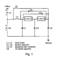
- Fig. 1 shows an embodiment of the invention, in which a ballast circuit runs two lamps.
- the ballast circuit is labeled by 2 ⁇ L36W circuit.
- Lamp 1 and Lamp 2 indicate two lamps connected in series.
- Capacitors C1 and C2 are ignition capacitors.
- Capacitors C3 and C4 are sequence start capacitors, and a capacitor C5 is a DC block capacitor.
- Coils L1 and L2 have a function as a lamp choke respectively.
- the capacitors C3 and C4 are connected through the filaments between both LC resonance circuits.
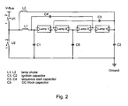
- Fig. 2 shows another embodiment of the invention, in which the ballast circuit runs four lamps.
- the ballast circuit is labeled by 4 ⁇ L18W circuit.
- Lamp 1, Lamp 2, Lamp 3 and Lamp 4 indicate four lamps connected in series.
- Capacitors C1 and C2 in respective LC resonance circuits are ignition capacitors.
- Capacitors C3 and C4 are sequence start capacitors, and a capacitor C5 is a DC block capacitor.
- Coils L1 and L2 in respective LC resonance circuits have a function as a lamp choke respectively.
- the four lamps are divided into two groups, one group comprises lamps Lamp 1 and Lamp 2, the other comprises lamps Lamp 3 and Lamp 4.
- the four lamps are connected in series, while the respective LC resonance circuits of each group are connected in parallel.
- the connection of the capacitors C3 and C4 is in a way extended from that shown in Fig. 1 .
- the capacitors C3 and C4 are connected to every other lamps, i.e. the capacitor C3 is connected across lamps Lamp 2 and Lamp 4, and capacitor C4 is connected across lamps Lamp 1 and Lamp 3. That is to say, the sequence start capacitors C3 and C4 are connected from each LC resonance circuit to the series connection point of the other group of lamps. By such a way it forms an arrangement of a ballast topologies of multiple load circuits.
- the ballast topologies further comprise two switches U1 and U2 for connecting the resonance circuits to a power supply.
- the capacitance values range of the sequence start capacitors C3 and C4 is from 140pF to 4.9nF
- the capacitance values range of the resonance capacitors C1 and C2 in the LC resonance circuits can be selected from 900pF to 16nF
- the induction values range of the coils L1 and L2 in the resonance circuits is from 950 ⁇ H to 8.4mH.
- the intended capacitance values range of the sequence start capacitors C3 and C4 is from 20pF to 900pF
- the intended capacitance values range of the resonance capacitors C1 and C2 in the LC resonance circuits can be selected from 200pF to 3.6nF
- the intended induction values range of the coils L1 and L2 in the resonance circuits is from 190 ⁇ H to 1.6mH.
- the number of the lamps in the topologies is not limited to the above-mentioned embodiments.
- the principle of the invention can be used for any other type of fluorescent lamps and also can be extended to any number of parallel resonance circuits.
Landscapes
- Circuit Arrangements For Discharge Lamps (AREA)
- Discharge Heating (AREA)
Abstract
Description
- The invention relates to a ballast circuit, specifically a ballast circuit for running multiple fluorescent lamps.
- In ballast topologies with multiple parallel load circuits for running plural fluorescent lamps, the element tolerances of the resonance circuit generally cause unbalanced resonance characteristics in the circuit. Also different load situations (e.g. a broken lamp) will cause severe unbalance in the ballast topologies. This results overload conditions, which are critical for conventional halfbridge switches and thus demand for a solution of high rate components.
- Basically in the art there are possibilities known to balance multiple load circuits by arranging a well-defined coupling between the different load circuits. However, such arrangement require more additional capacitors and/or magnetic elements that leads to compelexity in manufacturing process and will cause a cost-effectiveness problem in popular production.
-
WO 01/56337 A1 - The object of the invention is to provide an arrangement of ballast topologies for running multiple fluorescent lamps according to claim 1, in which no unbalance occurs even one of the fluorescent lamps is broken.
- Using sequence start capacitors for multiple lamps operation is well known in the art. However taking advantage of those sequence start capacitors to solve the unbalance caused by asymmetric LC resonance in parallel circuit is a new idea. Therefore the fundamental idea of the invention, is to use the already existing sequence start capacitors to set the required coupling of multiple load circuits.
- The object is achieved by a solution according to the teaching of claim 1.
- In the invention, the sequence start capacitors in parallel between LC resonance circuits are connected to other LC resonance circuit in a multiple lamp operation. By the solution of the invention, the problem of asymmetric LC resonance in parallel circuit is solved and the multiple lamp operation is implemented.
- The invention is explained with reference to the figures as below, in which:
-
Fig. 1 shows an embodiment of the invention, in which a ballast circuit runs two lamps; -
Fig. 2 shows another embodiment of the invention, in which a ballast circuit runs four lamps. -
Fig. 1 shows an embodiment of the invention, in which a ballast circuit runs two lamps. The ballast circuit is labeled by 2×L36W circuit. - As shown tin
Fig. 1 , Lamp 1 and Lamp 2 indicate two lamps connected in series. Capacitors C1 and C2 are ignition capacitors. Capacitors C3 and C4 are sequence start capacitors, and a capacitor C5 is a DC block capacitor. Coils L1 and L2 have a function as a lamp choke respectively. The capacitors C3 and C4 are connected through the filaments between both LC resonance circuits. - When a lamp Lamp 1, is broken, the coil L1 and capacitor C1 will generate a very high ignition voltage due to an asymmetric circuit load. By means of the sequence start capacitors C3 and C4, some of the current from the capacitor C1 is bypassed to the capacitor C5, the voltage of the capacitor C1. thus is decreased and limited, and the asymmetric resonance in the circuit is eliminated.
- The same process is carried out for the lamp Lamp 2. When the lamp Lamp 2 is broken, a very high voltage that will be generated by L2 and C2 is bypassed to the capacitor C5 by means of sequence start capacitors C3 and C4 so that the voltage on the capacitor C2 is limited to keep the balance in resonance in circuit.
-
Fig. 2 shows another embodiment of the invention, in which the ballast circuit runs four lamps. The ballast circuit is labeled by 4×L18W circuit. As shown inFig. 2 , Lamp 1, Lamp 2, Lamp 3 andLamp 4 indicate four lamps connected in series. Capacitors C1 and C2 in respective LC resonance circuits are ignition capacitors. Capacitors C3 and C4 are sequence start capacitors, and a capacitor C5 is a DC block capacitor. Coils L1 and L2 in respective LC resonance circuits have a function as a lamp choke respectively. - The four lamps are divided into two groups, one group comprises lamps Lamp 1 and Lamp 2, the other comprises lamps Lamp 3 and
Lamp 4. The four lamps are connected in series, while the respective LC resonance circuits of each group are connected in parallel. - The connection of the capacitors C3 and C4 is in a way extended from that shown in
Fig. 1 . The capacitors C3 and C4 are connected to every other lamps, i.e. the capacitor C3 is connected across lamps Lamp 2 andLamp 4, and capacitor C4 is connected across lamps Lamp 1 and Lamp 3. That is to say, the sequence start capacitors C3 and C4 are connected from each LC resonance circuit to the series connection point of the other group of lamps. By such a way it forms an arrangement of a ballast topologies of multiple load circuits. - When the lamp Lamp 1 is broken, the coil L1 and capacitor C1 will generate a very high ignition voltage due to an asymmetric circuit load. By means of the sequence start capacitors C3 and C4, some of the current from the capacitor C1 is bypassed to the capacitor C5, the voltage of the capacitor C1 thus is decreased and limited, and the asymmetric resonance in the circuit is eliminated.
- The same process is carried out for another lamps Lamp 2 in the same group.
- When the lamp Lamp 3 is broken, the coil L2 and capacitor C2 will generate a very high ignition voltage due to an asymmetric circuit load. By means of the sequence start capacitors C3 and C4, some of the current from the capacitor C2 is bypassed to the capacitor C5, the voltage of the capacitor C2 thus is decreased and limited, and the asymmetric resonance in the circuit is eliminated.
- The same process is carried out for another
lamps Lamp 4 in the same group. - The ballast topologies further comprise two switches U1 and U2 for connecting the resonance circuits to a power supply.
- For a ballast which operates in the frequency range of 20kHz to 100kHz, the capacitance values range of the sequence start capacitors C3 and C4 is from 140pF to 4.9nF, the capacitance values range of the resonance capacitors C1 and C2 in the LC resonance circuits can be selected from 900pF to 16nF, and the induction values range of the coils L1 and L2 in the resonance circuits is from 950µH to 8.4mH.
- For a ballast which operates in the frequency range of 100kHz to 500kHz, the intended capacitance values range of the sequence start capacitors C3 and C4 is from 20pF to 900pF, the intended capacitance values range of the resonance capacitors C1 and C2 in the LC resonance circuits can be selected from 200pF to 3.6nF, and the intended induction values range of the coils L1 and L2 in the resonance circuits is from 190µH to 1.6mH.
- It is understandable that the number of the lamps in the topologies is not limited to the above-mentioned embodiments. The principle of the invention can be used for any other type of fluorescent lamps and also can be extended to any number of parallel resonance circuits.
Claims (1)
- A ballast circuit for running a first, second, third and fourth fluorescent lamp (lamp 1, -2, -3, -4) connected in series in said order,
wherein the series connection of fluorescent lamps having a first end at the first fluorescent lamp (lamp 1) and a second end at the fourth fluorescent lamp (lamp 4),
wherein the first end and the second end is each connected to ground via resonance capacitors (C1, C2),
wherein the connection point between the second and the third lamp is connected to ground via a DC block capacitor (C5),
wherein the series connection of two switches (U2, U2) is connected between a DC-supply (V-Bus) and ground,
wherein the first end is connected to the connection point of the two switches via a first coil (L1),
wherein the second end is connected to the connection point of the two switches via a second coil (L2)
wherein the ballast circuit is characterized in
a first sequence start capacitor (C4) which is connected between the first end and the connection point of the third and the fourth fluorescent lamp (lamp 3, -4) and
a second sequence start capacitor (C3) which is connected between the second end and the connection point of the first and the second fluorescent lamp (lamp 1, -2).
Priority Applications (1)
| Application Number | Priority Date | Filing Date | Title |
|---|---|---|---|
| PL08845841T PL2206414T3 (en) | 2007-10-30 | 2008-10-09 | A ballast circuit |
Applications Claiming Priority (2)
| Application Number | Priority Date | Filing Date | Title |
|---|---|---|---|
| CN2007101657190A CN101426322B (en) | 2007-10-30 | 2007-10-30 | Ballast circuit |
| PCT/EP2008/063565 WO2009056431A2 (en) | 2007-10-30 | 2008-10-09 | A ballast circuit |
Publications (2)
| Publication Number | Publication Date |
|---|---|
| EP2206414A2 EP2206414A2 (en) | 2010-07-14 |
| EP2206414B1 true EP2206414B1 (en) | 2011-12-21 |
Family
ID=40380569
Family Applications (1)
| Application Number | Title | Priority Date | Filing Date |
|---|---|---|---|
| EP08845841A Not-in-force EP2206414B1 (en) | 2007-10-30 | 2008-10-09 | A ballast circuit |
Country Status (5)
| Country | Link |
|---|---|
| EP (1) | EP2206414B1 (en) |
| CN (1) | CN101426322B (en) |
| AT (1) | ATE538625T1 (en) |
| PL (1) | PL2206414T3 (en) |
| WO (1) | WO2009056431A2 (en) |
Families Citing this family (1)
| Publication number | Priority date | Publication date | Assignee | Title |
|---|---|---|---|---|
| CN102105013A (en) * | 2009-12-16 | 2011-06-22 | 奥斯兰姆有限公司 | Starting-assisting device, ballast and illumination device |
Family Cites Families (3)
| Publication number | Priority date | Publication date | Assignee | Title |
|---|---|---|---|---|
| US5747941A (en) * | 1995-12-07 | 1998-05-05 | Energy Savings, Inc. | Electronic ballast that monitors direct current through lamp filaments |
| US5636111A (en) * | 1996-03-26 | 1997-06-03 | The Genlyte Group Incorporated | Ballast shut-down circuit responsive to an unbalanced load condition in a single lamp ballast or in either lamp of a two-lamp ballast |
| US6366032B1 (en) * | 2000-01-28 | 2002-04-02 | Robertson Worldwide, Inc. | Fluorescent lamp ballast with integrated circuit |
-
2007
- 2007-10-30 CN CN2007101657190A patent/CN101426322B/en not_active Expired - Fee Related
-
2008
- 2008-10-09 PL PL08845841T patent/PL2206414T3/en unknown
- 2008-10-09 AT AT08845841T patent/ATE538625T1/en active
- 2008-10-09 WO PCT/EP2008/063565 patent/WO2009056431A2/en active Application Filing
- 2008-10-09 EP EP08845841A patent/EP2206414B1/en not_active Not-in-force
Also Published As
| Publication number | Publication date |
|---|---|
| CN101426322A (en) | 2009-05-06 |
| WO2009056431A2 (en) | 2009-05-07 |
| ATE538625T1 (en) | 2012-01-15 |
| WO2009056431A3 (en) | 2009-07-09 |
| CN101426322B (en) | 2013-01-02 |
| PL2206414T3 (en) | 2012-08-31 |
| EP2206414A2 (en) | 2010-07-14 |
Similar Documents
| Publication | Publication Date | Title |
|---|---|---|
| US6534934B1 (en) | Multi-lamp driving system | |
| KR100653292B1 (en) | Equalizing discharge lamp currents in cuircuits | |
| JP6397406B2 (en) | Drive circuit between fluorescent ballast and LED | |
| US20070247082A1 (en) | Discharge Lamp Operating Device | |
| KR20050045830A (en) | Drive circuit for illumination unit | |
| JP2009064789A (en) | Equalizing discharge lamp currents in circuits | |
| CA1317629C (en) | Electronic ballast for fluorescent lamps | |
| EP2206414B1 (en) | A ballast circuit | |
| US8587226B2 (en) | Driver system and method with cyclic configuration for multiple cold-cathode fluorescent lamps and/or external-electrode fluorescent lamps | |
| EP1843644B1 (en) | Discharge tube drive circuit | |
| WO2004064457A1 (en) | Circuit arrangment | |
| US7304441B2 (en) | Method and apparatus for driving discharge lamps in a floating configuration | |
| CN1893759B (en) | Smoothing circuit for improving EMC | |
| KR20080107998A (en) | Cold cathode fluorescent discharge lamp apparatus | |
| CN101115340B (en) | Inverter circuit | |
| CN101231907A (en) | Multi-light tube driving device and transformer thereof | |
| US9732914B2 (en) | LED lamp | |
| US20090039795A1 (en) | Discharge lamp lighting apparatus | |
| TW201012299A (en) | A driving system for driving backlight sources in an image display apparatus or for driving lamps in a multi-lamp lighting device | |
| CN106507559B (en) | Lighting device | |
| US8305002B2 (en) | Method and structure of forming a fluorescent lighting system | |
| JP4629613B2 (en) | Discharge tube drive circuit and inverter circuit | |
| US8264160B2 (en) | Advanced electronic ballasts | |
| JPH0947033A (en) | Power supply | |
| JP2004222481A (en) | Resonance converting circuit and constant current circuit |
Legal Events
| Date | Code | Title | Description |
|---|---|---|---|
| PUAI | Public reference made under article 153(3) epc to a published international application that has entered the european phase |
Free format text: ORIGINAL CODE: 0009012 |
|
| 17P | Request for examination filed |
Effective date: 20100514 |
|
| AK | Designated contracting states |
Kind code of ref document: A2 Designated state(s): AT BE BG CH CY CZ DE DK EE ES FI FR GB GR HR HU IE IS IT LI LT LU LV MC MT NL NO PL PT RO SE SI SK TR |
|
| AX | Request for extension of the european patent |
Extension state: AL BA MK RS |
|
| 17Q | First examination report despatched |
Effective date: 20110502 |
|
| GRAP | Despatch of communication of intention to grant a patent |
Free format text: ORIGINAL CODE: EPIDOSNIGR1 |
|
| DAX | Request for extension of the european patent (deleted) | ||
| RAP1 | Party data changed (applicant data changed or rights of an application transferred) |
Owner name: OSRAM AG |
|
| GRAS | Grant fee paid |
Free format text: ORIGINAL CODE: EPIDOSNIGR3 |
|
| GRAA | (expected) grant |
Free format text: ORIGINAL CODE: 0009210 |
|
| AK | Designated contracting states |
Kind code of ref document: B1 Designated state(s): AT BE BG CH CY CZ DE DK EE ES FI FR GB GR HR HU IE IS IT LI LT LU LV MC MT NL NO PL PT RO SE SI SK TR |
|
| REG | Reference to a national code |
Ref country code: GB Ref legal event code: FG4D |
|
| REG | Reference to a national code |
Ref country code: CH Ref legal event code: EP |
|
| REG | Reference to a national code |
Ref country code: AT Ref legal event code: REF Ref document number: 538625 Country of ref document: AT Kind code of ref document: T Effective date: 20120115 |
|
| REG | Reference to a national code |
Ref country code: IE Ref legal event code: FG4D |
|
| REG | Reference to a national code |
Ref country code: DE Ref legal event code: R096 Ref document number: 602008012250 Country of ref document: DE Effective date: 20120308 |
|
| REG | Reference to a national code |
Ref country code: NL Ref legal event code: VDEP Effective date: 20111221 |
|
| PG25 | Lapsed in a contracting state [announced via postgrant information from national office to epo] |
Ref country code: LT Free format text: LAPSE BECAUSE OF FAILURE TO SUBMIT A TRANSLATION OF THE DESCRIPTION OR TO PAY THE FEE WITHIN THE PRESCRIBED TIME-LIMIT Effective date: 20111221 Ref country code: NO Free format text: LAPSE BECAUSE OF FAILURE TO SUBMIT A TRANSLATION OF THE DESCRIPTION OR TO PAY THE FEE WITHIN THE PRESCRIBED TIME-LIMIT Effective date: 20120321 |
|
| LTIE | Lt: invalidation of european patent or patent extension |
Effective date: 20111221 |
|
| PG25 | Lapsed in a contracting state [announced via postgrant information from national office to epo] |
Ref country code: HR Free format text: LAPSE BECAUSE OF FAILURE TO SUBMIT A TRANSLATION OF THE DESCRIPTION OR TO PAY THE FEE WITHIN THE PRESCRIBED TIME-LIMIT Effective date: 20111221 Ref country code: SE Free format text: LAPSE BECAUSE OF FAILURE TO SUBMIT A TRANSLATION OF THE DESCRIPTION OR TO PAY THE FEE WITHIN THE PRESCRIBED TIME-LIMIT Effective date: 20111221 Ref country code: LV Free format text: LAPSE BECAUSE OF FAILURE TO SUBMIT A TRANSLATION OF THE DESCRIPTION OR TO PAY THE FEE WITHIN THE PRESCRIBED TIME-LIMIT Effective date: 20111221 Ref country code: GR Free format text: LAPSE BECAUSE OF FAILURE TO SUBMIT A TRANSLATION OF THE DESCRIPTION OR TO PAY THE FEE WITHIN THE PRESCRIBED TIME-LIMIT Effective date: 20120322 Ref country code: NL Free format text: LAPSE BECAUSE OF FAILURE TO SUBMIT A TRANSLATION OF THE DESCRIPTION OR TO PAY THE FEE WITHIN THE PRESCRIBED TIME-LIMIT Effective date: 20111221 Ref country code: SI Free format text: LAPSE BECAUSE OF FAILURE TO SUBMIT A TRANSLATION OF THE DESCRIPTION OR TO PAY THE FEE WITHIN THE PRESCRIBED TIME-LIMIT Effective date: 20111221 |
|
| PG25 | Lapsed in a contracting state [announced via postgrant information from national office to epo] |
Ref country code: CY Free format text: LAPSE BECAUSE OF FAILURE TO SUBMIT A TRANSLATION OF THE DESCRIPTION OR TO PAY THE FEE WITHIN THE PRESCRIBED TIME-LIMIT Effective date: 20111221 Ref country code: BE Free format text: LAPSE BECAUSE OF FAILURE TO SUBMIT A TRANSLATION OF THE DESCRIPTION OR TO PAY THE FEE WITHIN THE PRESCRIBED TIME-LIMIT Effective date: 20111221 |
|
| PG25 | Lapsed in a contracting state [announced via postgrant information from national office to epo] |
Ref country code: IS Free format text: LAPSE BECAUSE OF FAILURE TO SUBMIT A TRANSLATION OF THE DESCRIPTION OR TO PAY THE FEE WITHIN THE PRESCRIBED TIME-LIMIT Effective date: 20120421 Ref country code: EE Free format text: LAPSE BECAUSE OF FAILURE TO SUBMIT A TRANSLATION OF THE DESCRIPTION OR TO PAY THE FEE WITHIN THE PRESCRIBED TIME-LIMIT Effective date: 20111221 Ref country code: CZ Free format text: LAPSE BECAUSE OF FAILURE TO SUBMIT A TRANSLATION OF THE DESCRIPTION OR TO PAY THE FEE WITHIN THE PRESCRIBED TIME-LIMIT Effective date: 20111221 Ref country code: BG Free format text: LAPSE BECAUSE OF FAILURE TO SUBMIT A TRANSLATION OF THE DESCRIPTION OR TO PAY THE FEE WITHIN THE PRESCRIBED TIME-LIMIT Effective date: 20120321 Ref country code: SK Free format text: LAPSE BECAUSE OF FAILURE TO SUBMIT A TRANSLATION OF THE DESCRIPTION OR TO PAY THE FEE WITHIN THE PRESCRIBED TIME-LIMIT Effective date: 20111221 |
|
| PG25 | Lapsed in a contracting state [announced via postgrant information from national office to epo] |
Ref country code: RO Free format text: LAPSE BECAUSE OF FAILURE TO SUBMIT A TRANSLATION OF THE DESCRIPTION OR TO PAY THE FEE WITHIN THE PRESCRIBED TIME-LIMIT Effective date: 20111221 Ref country code: PT Free format text: LAPSE BECAUSE OF FAILURE TO SUBMIT A TRANSLATION OF THE DESCRIPTION OR TO PAY THE FEE WITHIN THE PRESCRIBED TIME-LIMIT Effective date: 20120423 |
|
| REG | Reference to a national code |
Ref country code: PL Ref legal event code: T3 |
|
| REG | Reference to a national code |
Ref country code: AT Ref legal event code: MK05 Ref document number: 538625 Country of ref document: AT Kind code of ref document: T Effective date: 20111221 |
|
| PLBE | No opposition filed within time limit |
Free format text: ORIGINAL CODE: 0009261 |
|
| STAA | Information on the status of an ep patent application or granted ep patent |
Free format text: STATUS: NO OPPOSITION FILED WITHIN TIME LIMIT |
|
| PG25 | Lapsed in a contracting state [announced via postgrant information from national office to epo] |
Ref country code: DK Free format text: LAPSE BECAUSE OF FAILURE TO SUBMIT A TRANSLATION OF THE DESCRIPTION OR TO PAY THE FEE WITHIN THE PRESCRIBED TIME-LIMIT Effective date: 20111221 |
|
| 26N | No opposition filed |
Effective date: 20120924 |
|
| PG25 | Lapsed in a contracting state [announced via postgrant information from national office to epo] |
Ref country code: IT Free format text: LAPSE BECAUSE OF FAILURE TO SUBMIT A TRANSLATION OF THE DESCRIPTION OR TO PAY THE FEE WITHIN THE PRESCRIBED TIME-LIMIT Effective date: 20111221 |
|
| REG | Reference to a national code |
Ref country code: DE Ref legal event code: R097 Ref document number: 602008012250 Country of ref document: DE Effective date: 20120924 |
|
| PG25 | Lapsed in a contracting state [announced via postgrant information from national office to epo] |
Ref country code: AT Free format text: LAPSE BECAUSE OF FAILURE TO SUBMIT A TRANSLATION OF THE DESCRIPTION OR TO PAY THE FEE WITHIN THE PRESCRIBED TIME-LIMIT Effective date: 20111221 |
|
| REG | Reference to a national code |
Ref country code: DE Ref legal event code: R081 Ref document number: 602008012250 Country of ref document: DE Owner name: OSRAM GMBH, DE Free format text: FORMER OWNER: OSRAM AG, 81543 MUENCHEN, DE Effective date: 20130205 |
|
| PG25 | Lapsed in a contracting state [announced via postgrant information from national office to epo] |
Ref country code: ES Free format text: LAPSE BECAUSE OF FAILURE TO SUBMIT A TRANSLATION OF THE DESCRIPTION OR TO PAY THE FEE WITHIN THE PRESCRIBED TIME-LIMIT Effective date: 20120401 |
|
| PG25 | Lapsed in a contracting state [announced via postgrant information from national office to epo] |
Ref country code: MC Free format text: LAPSE BECAUSE OF NON-PAYMENT OF DUE FEES Effective date: 20121031 |
|
| REG | Reference to a national code |
Ref country code: CH Ref legal event code: PL |
|
| REG | Reference to a national code |
Ref country code: IE Ref legal event code: MM4A |
|
| PG25 | Lapsed in a contracting state [announced via postgrant information from national office to epo] |
Ref country code: CH Free format text: LAPSE BECAUSE OF NON-PAYMENT OF DUE FEES Effective date: 20121031 Ref country code: LI Free format text: LAPSE BECAUSE OF NON-PAYMENT OF DUE FEES Effective date: 20121031 Ref country code: IE Free format text: LAPSE BECAUSE OF NON-PAYMENT OF DUE FEES Effective date: 20121009 |
|
| REG | Reference to a national code |
Ref country code: DE Ref legal event code: R081 Ref document number: 602008012250 Country of ref document: DE Owner name: OSRAM GMBH, DE Free format text: FORMER OWNER: OSRAM GMBH, 81543 MUENCHEN, DE Effective date: 20130823 |
|
| PG25 | Lapsed in a contracting state [announced via postgrant information from national office to epo] |
Ref country code: MT Free format text: LAPSE BECAUSE OF FAILURE TO SUBMIT A TRANSLATION OF THE DESCRIPTION OR TO PAY THE FEE WITHIN THE PRESCRIBED TIME-LIMIT Effective date: 20111221 |
|
| PG25 | Lapsed in a contracting state [announced via postgrant information from national office to epo] |
Ref country code: TR Free format text: LAPSE BECAUSE OF FAILURE TO SUBMIT A TRANSLATION OF THE DESCRIPTION OR TO PAY THE FEE WITHIN THE PRESCRIBED TIME-LIMIT Effective date: 20111221 |
|
| PG25 | Lapsed in a contracting state [announced via postgrant information from national office to epo] |
Ref country code: LU Free format text: LAPSE BECAUSE OF NON-PAYMENT OF DUE FEES Effective date: 20121009 |
|
| PG25 | Lapsed in a contracting state [announced via postgrant information from national office to epo] |
Ref country code: HU Free format text: LAPSE BECAUSE OF FAILURE TO SUBMIT A TRANSLATION OF THE DESCRIPTION OR TO PAY THE FEE WITHIN THE PRESCRIBED TIME-LIMIT Effective date: 20081009 |
|
| PGFP | Annual fee paid to national office [announced via postgrant information from national office to epo] |
Ref country code: PL Payment date: 20140922 Year of fee payment: 7 |
|
| PGFP | Annual fee paid to national office [announced via postgrant information from national office to epo] |
Ref country code: FR Payment date: 20141022 Year of fee payment: 7 |
|
| REG | Reference to a national code |
Ref country code: FR Ref legal event code: ST Effective date: 20160630 |
|
| PG25 | Lapsed in a contracting state [announced via postgrant information from national office to epo] |
Ref country code: FR Free format text: LAPSE BECAUSE OF NON-PAYMENT OF DUE FEES Effective date: 20151102 |
|
| PGFP | Annual fee paid to national office [announced via postgrant information from national office to epo] |
Ref country code: GB Payment date: 20161020 Year of fee payment: 9 Ref country code: FI Payment date: 20161012 Year of fee payment: 9 Ref country code: DE Payment date: 20161020 Year of fee payment: 9 |
|
| PG25 | Lapsed in a contracting state [announced via postgrant information from national office to epo] |
Ref country code: PL Free format text: LAPSE BECAUSE OF NON-PAYMENT OF DUE FEES Effective date: 20151009 |
|
| REG | Reference to a national code |
Ref country code: DE Ref legal event code: R119 Ref document number: 602008012250 Country of ref document: DE |
|
| GBPC | Gb: european patent ceased through non-payment of renewal fee |
Effective date: 20171009 |
|
| PG25 | Lapsed in a contracting state [announced via postgrant information from national office to epo] |
Ref country code: GB Free format text: LAPSE BECAUSE OF NON-PAYMENT OF DUE FEES Effective date: 20171009 Ref country code: DE Free format text: LAPSE BECAUSE OF NON-PAYMENT OF DUE FEES Effective date: 20180501 Ref country code: FI Free format text: LAPSE BECAUSE OF NON-PAYMENT OF DUE FEES Effective date: 20171009 |