EP2202884B1 - Electric circuit with self-conducting semiconductor switch - Google Patents
Electric circuit with self-conducting semiconductor switch Download PDFInfo
- Publication number
- EP2202884B1 EP2202884B1 EP08172700A EP08172700A EP2202884B1 EP 2202884 B1 EP2202884 B1 EP 2202884B1 EP 08172700 A EP08172700 A EP 08172700A EP 08172700 A EP08172700 A EP 08172700A EP 2202884 B1 EP2202884 B1 EP 2202884B1
- Authority
- EP
- European Patent Office
- Prior art keywords
- circuit
- voltage
- voltage source
- inverter bridge
- input lines
- Prior art date
- Legal status (The legal status is an assumption and is not a legal conclusion. Google has not performed a legal analysis and makes no representation as to the accuracy of the status listed.)
- Not-in-force
Links
Images


Classifications
-
- H—ELECTRICITY
- H02—GENERATION; CONVERSION OR DISTRIBUTION OF ELECTRIC POWER
- H02M—APPARATUS FOR CONVERSION BETWEEN AC AND AC, BETWEEN AC AND DC, OR BETWEEN DC AND DC, AND FOR USE WITH MAINS OR SIMILAR POWER SUPPLY SYSTEMS; CONVERSION OF DC OR AC INPUT POWER INTO SURGE OUTPUT POWER; CONTROL OR REGULATION THEREOF
- H02M7/00—Conversion of ac power input into dc power output; Conversion of dc power input into ac power output
- H02M7/42—Conversion of dc power input into ac power output without possibility of reversal
- H02M7/44—Conversion of dc power input into ac power output without possibility of reversal by static converters
- H02M7/48—Conversion of dc power input into ac power output without possibility of reversal by static converters using discharge tubes with control electrode or semiconductor devices with control electrode
-
- H—ELECTRICITY
- H03—ELECTRONIC CIRCUITRY
- H03K—PULSE TECHNIQUE
- H03K17/00—Electronic switching or gating, i.e. not by contact-making and –breaking
- H03K17/06—Modifications for ensuring a fully conducting state
- H03K17/063—Modifications for ensuring a fully conducting state in field-effect transistor switches
-
- H—ELECTRICITY
- H02—GENERATION; CONVERSION OR DISTRIBUTION OF ELECTRIC POWER
- H02M—APPARATUS FOR CONVERSION BETWEEN AC AND AC, BETWEEN AC AND DC, OR BETWEEN DC AND DC, AND FOR USE WITH MAINS OR SIMILAR POWER SUPPLY SYSTEMS; CONVERSION OF DC OR AC INPUT POWER INTO SURGE OUTPUT POWER; CONTROL OR REGULATION THEREOF
- H02M1/00—Details of apparatus for conversion
- H02M1/32—Means for protecting converters other than automatic disconnection
-
- H—ELECTRICITY
- H03—ELECTRONIC CIRCUITRY
- H03K—PULSE TECHNIQUE
- H03K17/00—Electronic switching or gating, i.e. not by contact-making and –breaking
- H03K17/16—Modifications for eliminating interference voltages or currents
- H03K17/161—Modifications for eliminating interference voltages or currents in field-effect transistor switches
- H03K17/162—Modifications for eliminating interference voltages or currents in field-effect transistor switches without feedback from the output circuit to the control circuit
-
- H—ELECTRICITY
- H03—ELECTRONIC CIRCUITRY
- H03K—PULSE TECHNIQUE
- H03K17/00—Electronic switching or gating, i.e. not by contact-making and –breaking
- H03K17/20—Modifications for resetting core switching units to a predetermined state
-
- H—ELECTRICITY
- H03—ELECTRONIC CIRCUITRY
- H03K—PULSE TECHNIQUE
- H03K17/00—Electronic switching or gating, i.e. not by contact-making and –breaking
- H03K17/06—Modifications for ensuring a fully conducting state
- H03K2017/066—Maximizing the OFF-resistance instead of minimizing the ON-resistance
-
- H—ELECTRICITY
- H03—ELECTRONIC CIRCUITRY
- H03K—PULSE TECHNIQUE
- H03K17/00—Electronic switching or gating, i.e. not by contact-making and –breaking
- H03K17/51—Electronic switching or gating, i.e. not by contact-making and –breaking characterised by the components used
- H03K17/56—Electronic switching or gating, i.e. not by contact-making and –breaking characterised by the components used by the use, as active elements, of semiconductor devices
- H03K17/687—Electronic switching or gating, i.e. not by contact-making and –breaking characterised by the components used by the use, as active elements, of semiconductor devices the devices being field-effect transistors
- H03K2017/6875—Electronic switching or gating, i.e. not by contact-making and –breaking characterised by the components used by the use, as active elements, of semiconductor devices the devices being field-effect transistors using self-conductive, depletion FETs
-
- Y—GENERAL TAGGING OF NEW TECHNOLOGICAL DEVELOPMENTS; GENERAL TAGGING OF CROSS-SECTIONAL TECHNOLOGIES SPANNING OVER SEVERAL SECTIONS OF THE IPC; TECHNICAL SUBJECTS COVERED BY FORMER USPC CROSS-REFERENCE ART COLLECTIONS [XRACs] AND DIGESTS
- Y02—TECHNOLOGIES OR APPLICATIONS FOR MITIGATION OR ADAPTATION AGAINST CLIMATE CHANGE
- Y02E—REDUCTION OF GREENHOUSE GAS [GHG] EMISSIONS, RELATED TO ENERGY GENERATION, TRANSMISSION OR DISTRIBUTION
- Y02E10/00—Energy generation through renewable energy sources
- Y02E10/50—Photovoltaic [PV] energy
- Y02E10/56—Power conversion systems, e.g. maximum power point trackers
Definitions
- the invention relates to an electrical circuit having the features of the preamble of independent claim 1, which is also referred to as an inverter.
- the present invention relates to inverters for feeding electrical energy from a DC power source to an AC power grid.
- the DC voltage source may be a photovoltaic system.
- An inverter as it is in particular the subject of the present invention, but can also be used for other purposes, wherein the frequency of the AC output voltage to which the inverter is directed, constant or variable, for example, to drive an AC motor.
- an inverter according to the invention can be provided for single-phase alternating current or multi-phase, in particular three-phase, three-phase current, even if only a single-phase inverter is described below.
- a combination of the inverter with other electrical or electronic units, such as an upstream boost converter or the like is possible.
- the present invention then relates to the structure of the inverter as such.
- An inverter having a H-shaped inverter bridge between two input lines, the inverter bridge having semiconductor switches, and one of the Semiconductor switch in operation of the inverter clocking control is eg from the DE 10 2004 030 912 B3 known.
- the semiconductor switches as MOSFET semiconductor devices, ie formed as a metal-oxide-semiconductor field effect transistor.
- Such field effect transistors are self-locking, ie they do not conduct without driving their control terminal. This is advantageous insofar as that the entire inverter bridge does not conduct without triggering the control connections of the semiconductor switches and thus prevents a short circuit between the input lines and also an output-side AC voltage network.
- an input voltage can build up across the inverter bridge, which can be used as a supply voltage for the controller.
- This case occurs, for example, when using the known inverter for feeding electrical energy from a photovoltaic system into an AC grid in the morning, when the photovoltaic system starts to generate electricity.
- Specially is in the from the DE 10 2004 030 912 B3 known inverter in one of the input lines an additional, designed as a MOSFET semiconductor device semiconductor switch is provided, which is clocked as well as provided in the connected to the other input line branches of the inverter bridge semiconductor switch with a higher frequency, while the other two semiconductor switches of the inverter bridge with a lower Frequency are clocked.
- This lower frequency corresponds to the frequency to which the inverter is aimed, while the higher frequency is used to shape the generated alternating current by means of pulse width modulation.
- All designed as MOSFET semiconductor devices semiconductor switches are provided in the known inverter with anti-parallel diodes.
- JFETs SiC-based junction field effect transistors
- JFETs are generally normally-on semiconductor devices, i. H. They conduct without a voltage applied to their control terminal.
- a so-called cascode circuit is known as an electrical circuit having the features of the preamble of independent claim 1, in which a JFET is combined with a MOSFET and in which an input voltage is applied to the control terminal of the JFET and via the MOSFET Source of the JFET is branched.
- the JFET is switched indirectly in the cascode circuit. It is advantageous that the blocking capability of the SiC-JFET is used and the MOSFET has to have only a low blocking voltage resistance.
- the power current also flows through the MOSFET, which significantly influences the switching behavior of the entire cascode, so that a cascode is burdened with all the other disadvantages of a MOSFET compared to a JFET.
- the normally-on semiconductor switches are each provided in a cascode circuit.
- the advantages of a JFET can be exploited only to a very limited extent, in particular the advantages of an SiC-based JFET, since its high temperature resistance is insignificant in view of the lower temperature resistance of the MOSFET in the same cascode.
- the number of semiconductor switches due to a JFET and a MOSFET for each switching unit is twice as large as actually needed.
- EP 1 768 251 A1 is a protective circuit for a synchronous motor with permanent magnets known in which self-locking switch an inverter bridge for controlling the motor are also placed in defined switching states when a main power supply of the controller fails.
- a replacement power supply for the controller is provided in addition to the main energy supply. Both the main power supply and the spare power supply are fed from the input voltage of the inverter bridge.
- WO 02/50897 A2 From the WO 02/50897 A2 is a power electronic circuit in the form of an inverter bridge with normally-on semiconductor switches known.
- a controller clocking the semiconductor switches is powered from an input voltage of the inverter bridge with electrical energy.
- a diode and a capacitor are connected in series between the input lines. The capacitor keeps its charge due to the diode even if the voltage between the input lines collapses. In this way, the power supply of the controller, which is based on the voltage across this capacitor, also remains for some time after such a breakdown.
- the invention has for its object to provide an electrical circuit with the features of the preamble of independent claim 1, in which a short circuit between the input lines of the circuit in each operating state is reliably avoided, even if only a small voltage applied to the circuit.
- the new electrical circuit with the at least one normally-on semiconductor switch is in turn self-conducting between the input lines. That is, the normally-on semiconductor switches are not connected in series in the manner of a cascode with a self-locking semiconductor switch and clocked indirectly via such a self-locking semiconductor switch. Rather, the control of the new circuit controls the control terminals of the normally-on semiconductor switches directly with control voltages.
- a DC voltage source is provided, which applies a blocking potential to the control terminal of the normally-on semiconductor switch in the event of failure of the controller. This DC voltage source can be kept simple because only small amounts of charge are required for the application of the blocking potential to a normally-on semiconductor switch.
- no component is typically connected in the new circuit via which current continuously flows during the operation of the circuit, which would also cause a power loss.
- the DC voltage source of the new circuit is based on an electric charge storage.
- This memory has a rechargeable via the circuit accumulator or capacitor. Although electrical power is consumed for charging the accumulator or capacitor, this is not constant and, given appropriate dimensioning of the accumulator for electrical charge, only to a small extent.
- the DC voltage source has a charging circuit connected in series between the input lines to a further normally-on semiconductor switch for the electric charge storage, e.g. As a phtovoltaic MOSFET driver, as offered by the company Panasonic under the name Solardrive, on.
- the charging circuit charges the electric charge storage device while the current is flowing, and the electric potential accumulator voltage serving as a blocking potential is also applied to the control terminal of the further self-conducting semiconductor switch.
- the current through the charging circuit is accordingly blocked when the storage is charged for electrical charge. That is, only a small amount of current flows through the charging circuit. In addition, this current flows with a suitable design of the charging circuit already when only a low voltage is applied to the circuit.
- the charging circuit is protected from higher voltages by the self-conducting semiconductor switch which is connected in series with it and which is blocked when the accumulator is charged for electrical charging.
- the DC voltage source which applies the blocking potentials to the normally-open semiconductor switches of the new circuit, from the conductive semiconductor switches, if it is not needed, so that on the one hand, the control is not disturbed when driving the semiconductor switches and on the other hand, the DC voltage source is not unnecessarily burdened, can be arranged between the DC voltage source and the control terminals of the normally-on semiconductor terminals, a controllable switching element whose control terminal controls the control during operation of the circuit with a control voltage to lock it.
- a switching element is sufficient for a plurality of self-conducting semiconductor switches; but controlled by the DC voltage source control terminals of a plurality of normally-on semiconductor switches are to be decoupled from each other by blocking diodes.
- a DC voltage is applied as an input voltage between the input lines. At least the input voltage is of fixed polarity.
- the DC voltage source does not have to apply a blocking potential to each of the normally-open semiconductor switches in order to prevent a short circuit between the input lines. Rather, a subset of the semiconductor switches of the inverter bridge can be selected for this purpose. Such a selection would be, for example, depending on a self-conducting semiconductor switch per branch of the inverter bridge, said semiconductor switches are all arranged in outgoing from the same input line lines of the inverter bridge.
- this alternating voltage can also be used to feed the DC voltage source according to the invention for providing the blocking potentials.
- the AC voltage is preferably rectified, but it can also be charged a memory for electrical charge to ensure the function of the DC voltage source even in case of failure of the AC voltage.
- the self-conducting semiconductor switches of the new circuit may preferably be formed on SiC basis.
- Their basic structure may be field-effect transistors.
- the field effect transistors are so-called JFETs.
- a buffer capacitor can be connected between the input lines.
- At least one inductor can be connected in the shunt branch of the inverter bridge.
- Such an inductance can also be arranged on both sides of the AC voltage tapping point provided there. This is from the DE 10 2004 030 912 B3 known measure.
- An inverter designed according to the present invention is particularly suitable for feeding electrical energy from a DC voltage source into an AC voltage network.
- the DC voltage source may be a battery, a fuel cell, a fuel cell stack or the like.
- the DC voltage source is a photovoltaic system.
- a circuit according to the invention and thus also an inverter according to the invention can be implemented in a wide variety of environments and can be integrated into a wide variety of circuits, as is generally known to the person skilled in the art.
- These include the rectifier topologies known by the keywords H4, H5, Heric, 3-level, 5-level and Gonzales.
- electrical circuit 1 has a normally-on semiconductor switch 2 between two input lines 3 and 4. Since the semiconductor switch 2 here is the only component which is connected between the input lines 3 and 4, the circuit 1 between the input lines 3 and 4 without driving the semiconductor switch 2 is in turn self-conducting.
- a controller 5 controls the control terminal 6 of the semiconductor switch 2 with control voltages 7 in order to clock the semiconductor switch 2 during operation of the circuit 1.
- a DC voltage source 11 is provided which applies a blocking potential 12 to the control terminal 6.
- the DC voltage source here has a removable battery 36.
- a further self-conducting semiconductor switch 8 is provided in the line between the DC voltage source 11 and the control terminal 6, whose control terminal 9 is subjected to a blocking potential 10 during operation of the circuit 1 by the controller 5, so that he locks.
- the controller 5 eliminates the blocking potential 10, and the blocking potential 12 from the DC voltage source 11 is applied to the control terminal 6 of the semiconductor switch 2 and blocks it.
- the control unit is supplied with a reference potential from the input line 4.
- a dashed line is in Fig. 1 a subcircuit 28 surrounded, which forms a gate circuit of the control terminal 6 of the semiconductor switch 1.
- the circuit 1 according to Fig. 2 differs from the one according to Fig. 1 in that the DC voltage source 11 here has a capacitor 13 as an accumulator 14 for electrical charge.
- the capacitor 14 is charged by the controller 5 via a line 32 from a voltage applied between the input lines 3 and 4 and tapped with lines 31 and 32 voltage.
- the charge is held by a blocking diode 15 even at a drop in the control 5 on the capacitor 14, so that a DC voltage for applying the blocking potential 12 to the control terminal 6 of the semiconductor switch. 2 ready.
- a dashed line is in Fig. 2 a subcircuit 30 surrounded, which forms a gate circuit of the control terminal 6 of the semiconductor switch 1.
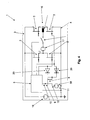
- Fig. 3 shows a circuit 1, which has an inverter bridge 16 with here total 4 self-conducting semiconductor switches 2 between the input lines 3 and 4.
- the two branches of the inverter bridge 16 running parallel between the input lines 3 and 4 each comprise two semiconductor switches 2, between which one of two poles of an AC voltage tapping point 17 is formed.
- the AC voltage tapping point 17 is connected in series with an inductance 21 between the branches of the inverter bridge 16.
- the thus formed inverter for a voltage applied to the input lines 3 and 4 DC voltage of an external voltage source 18 may additionally have a buffer capacitor 19, not shown here, parallel to the inverter bridge 16 between the input line 3 and 4 connected.
- Such a buffer capacitor is then typically significantly larger in size, ie it has a much larger capacity than the capacitor 13, with which only the small charges must be provided to block the inverter bridge 16 in the event of failure of the controller, not shown here.
- the blocking takes place here only via the two lower semiconductor switches 2 of the inverter bridge 16, which are provided in the outgoing of the input line 4 lines of the inverter bridge 16.
- these two lower semiconductor switches turn off, current can no longer flow across the inverter bridge 16 between the input lines 3 and 4, and in particular the charges on the buffer capacitor 19 can not balance in an uncontrolled manner across the inverter bridge 16, thereby jeopardizing the inventory of the inverter bridge 16 Generate electricity.
- the controller controls a network relay 34 for connecting the DC voltage source 18 to an AC power supply connected to the AC tapping point 17.
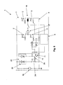
- the circuit 1 according to Fig. 4 not up.
- the blocking potential 12 is applied by the again formed with a battery 36 as a memory for electric charge DC voltage source 11 in case of failure of all four semiconductor switches 2 of the inverter bridge 16, and these blocking potentials are also at the beginning, d h.
- the external DC voltage source 18 is a photovoltaic system whose output voltage starts at zero in the morning.
- the DC voltage source 11 is combined with a charging circuit 23 which is based on a photovoltaic MOSFET driver 22.
- the charging circuit 23 is connected in series with a further normally-on semiconductor switch 24 between the input lines 3 and 4.
- the control terminal 25 of the semiconductor switch 24 is acted upon by the output voltage of the DC voltage source 11 as a blocking potential. That is, current only flows through the semiconductor switch 24 when the output voltage of the DC power source 11 is low. Then, the current flowing through the charging circuit 23 causes an output side current to charge the DC voltage source 11 and its electric charge storage, respectively, until its output voltage blocks the normally-on semiconductor switch.
- the memory for electrical charge of the DC voltage source 11 may be, for example, a capacitor 13 of small capacity, which is then charged by an input-side current through the charging circuit 23, when the inverter bridge 16 is still self-conducting, because the internal resistance of the charging circuit 23 in the series circuit the self-conductive semiconductor switch 24 is of the same order of magnitude as that of the self-conducting inverter bridge 16.
- the output current of a photovoltaic system as external voltage source 18 first charge the DC voltage source 11, wherein between the input lines 3 and 4 is applied only a small harmless voltage. Then, all the normally-on semiconductor switches 2 and 24 are disabled, and the working output voltage of the photovoltaic system 18 can build up.
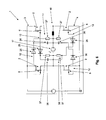
- the DC voltage source 11 was supplied to provide the blocking potentials via the input lines 3 and 4, it is in the embodiment according to Fig. 6 fed via the AC tapping point 17, that is, from an external AC voltage applied here, for example, that of an AC mains, into which the circuit 1 current from a photovoltaic system is fed.
- the alternating voltage applied to the alternating voltage tapping point 17 is rectified with rectifier diodes 26 in order to provide the blocking potentials 12.
- Resistors 37 and capacitors 38 serve to limit the current flowing to the control terminals 6 of the semiconductor switch 2 and the voltage of the blocking potentials.
- a memory for electric charge is in the circuit 1 according to Fig. 6 not provided.
Landscapes
- Engineering & Computer Science (AREA)
- Power Engineering (AREA)
- Inverter Devices (AREA)
- Electronic Switches (AREA)
- Charge And Discharge Circuits For Batteries Or The Like (AREA)
- Power Conversion In General (AREA)
Abstract
Description
Die Erfindung bezieht sich auf einen elektrische Schaltung mit den Merkmalen des Oberbegriffs des unabhängigen Patentanspruchs 1, die auch als Wechselrichter zu bezeichnen ist.The invention relates to an electrical circuit having the features of the preamble of
Insbesondere bezieht sich die vorliegende Erfindung auf Wechselrichter zur Einspeisung von elektrischer Energie von einer Gleichspannungsquelle in ein Wechselspannungsnetz. Noch spezieller kann die Gleichspannungsquelle dabei eine Photovoltaikanlage sein.In particular, the present invention relates to inverters for feeding electrical energy from a DC power source to an AC power grid. More specifically, the DC voltage source may be a photovoltaic system.
Ein Wechselrichter, wie er insbesondere Gegenstand der vorliegenden Erfindung ist, kann aber auch zu anderen Zwecken verwendet werden, wobei die Frequenz der Ausgangswechselspannung, auf die der Wechselrichter richtet, konstant oder variabel sein kann, um beispielsweise einen Wechselspannungsmotor anzusteuern.An inverter, as it is in particular the subject of the present invention, but can also be used for other purposes, wherein the frequency of the AC output voltage to which the inverter is directed, constant or variable, for example, to drive an AC motor.
Weiterhin kann ein erfindungsgemäßer Wechselrichter für einphasigen Wechselstrom oder mehrphasigen, insbesondere dreiphasigen Drehstrom vorgesehen sein, selbst wenn im Folgenden nur ein einphasiger Wechselrichter beschrieben ist. Auch eine Kombination des Wechselrichters mit weiteren elektrischen oder elektronischen Einheiten, wie beispielsweise einem vorgeschalteten Hochsetzsteller oder dergleichen ist möglich. Die vorliegende Erfindung betrifft dann den Aufbau des Wechselrichters als solchen.Furthermore, an inverter according to the invention can be provided for single-phase alternating current or multi-phase, in particular three-phase, three-phase current, even if only a single-phase inverter is described below. A combination of the inverter with other electrical or electronic units, such as an upstream boost converter or the like is possible. The present invention then relates to the structure of the inverter as such.
Ein Wechselrichter mit einer H-förmigen Wechselrichterbrücke zwischen zwei Eingangsleitungen, wobei die Wechselrichterbrücke Halbleiterschalter aufweist, und mit einer die Halbleiterschalter im Betrieb des Wechselrichters taktenden Steuerung ist z.B. aus der
Über einen Rekord für den Wirkungsgrad eines Wechselrichters wird in einer Presseinformation Nr. 02/08 des Fraunhofer-Instituts für Solare Energiesysteme ISE vom 15. Januar 2008 (http://www.ise.fhg.de/presse-und-medien/presseinformationenpdf/0208_ISE_PI_d_Rekord_Wechselrichterwirkungsgrad.pdf) berichtet. Bei dem Wechselrichter, der Gegenstand der Presseinformation ist, wurden MOSFETs auf Basis des Halbleiters Siliziumkarbid (SiC) verwendet. Von SiC-Halbleiterbauelementen ist nicht nur bekannt, dass sie sehr gute Eigenschaften wie niedrige Durchlass- und Schaltverluste aufweisen, sondern auch, dass sie jenseits des Temperaturbereichs, in dem Siliziumhalbleiterbauelemente funktionsfähig sind, d. h. bis zu 600°C, einsetzbar sind. Bei MOSFETs auf der Basis von SiC handelt es sich jedoch um nicht allgemein verfügbare Halbleiterbauelemente, die daher zumindest derzeit noch keinen umfangreichen Einsatz bei Wechselrichtern finden können und die in der derzeitigen Ausführung wiederum eine Temperaturbegrenzung aufweisen.About a record for the efficiency of an inverter is in a press release No. 02/08 of the Fraunhofer Institute for Solar Energy Systems ISE from January 15, 2008 (http://www.ise.fhg.de/presse-und-medien/presseinformationenpdf /0208_ISE_PI_d_Record_Inverter_efficiency.pdf). In the inverter which is the subject of the press release, MOSFETs based on the semiconductor silicon carbide (SiC) have been used. SiC semiconductor devices are not only known to have very good properties, such as low on-state and switching losses, but also to be usable beyond the temperature range in which silicon semiconductor devices are functional, ie up to 600 ° C. SiC-based MOSFETs, however, are not generally available semiconductor devices, and therefore, at least for the time being, they are not widely used Inverters can find and in the current design again have a temperature limit.
Zu vertretbaren Bedingungen verfügbar sind hingegen Sperrschicht-Feldeffekttransistoren (JFETs) auf SiC-Basis. JFETs sind jedoch im Allgemeinen selbstleitende Halbleiterbauelemente, d. h. sie leiten, ohne dass eine Spannung an ihrem Steueranschluss anliegt. Um diesen Nachteil zu kompensieren, ist eine sogenannte Kaskoden-Schaltung als elektrische Schaltung mit den Merkmalen des Oberbegriffs des unabhängigen Patentanspruchs 1 bekannt, bei der ein JFET mit einem MOSFET kombiniert ist und bei der eine Eingangsspannung auf den Steueranschluss des JFETs und über den MOSFET zur Source des JFETs verzweigt ist. Mittels Ansteuerung des Steueranschlusses des MOSFETs wird der JFET bei der Kaskodenschaltung indirekt geschaltet. Dabei ist von Vorteil, dass das Sperrvermögen des SiC-JFET genutzt wird und der MOSFET nur eine geringe Sperrspannungsfestigkeit aufweisen muss. Allerdings fließt der Leistungsstrom auch über den MOSFET, welcher das Schaltverhalten der gesamten Kaskode maßgeblich beeinflusst, so dass eine Kaskode mit allen weiteren Nachteilen eines MOSFETs gegenüber einem JFET belastet ist.At reasonable conditions, however, are SiC-based junction field effect transistors (JFETs). However, JFETs are generally normally-on semiconductor devices, i. H. They conduct without a voltage applied to their control terminal. To compensate for this disadvantage, a so-called cascode circuit is known as an electrical circuit having the features of the preamble of
Bei einem bekannten Wechselrichter mit einer Wechselrichterbrücke auf Basis selbstleitender Halbleiterschalter sind die selbstleitenden Halbleiterschalter jeweils in einer Kaskodenschaltung vorgesehen. Wie voranstehend erläutert wurde, können so die Vorteile eines JFET nur sehr begrenzt ausgenutzt werden, insbesondere die Vorteile eines JFET auf SiC-Basis, da dessen hohe Temperaturbeständigkeit angesichts der geringeren Temperaturbeständigkeit des MOSFETs in derselben Kaskode unbedeutend ist. Zudem ist die Anzahl der Halbleiterschalter aufgrund eines JFETs und eines MOSFETs für jede schaltende Einheit doppelt so groß wie eigentlich nötig.In a known inverter with an inverter bridge based on self-conducting semiconductor switches, the normally-on semiconductor switches are each provided in a cascode circuit. As explained above, the advantages of a JFET can be exploited only to a very limited extent, in particular the advantages of an SiC-based JFET, since its high temperature resistance is insignificant in view of the lower temperature resistance of the MOSFET in the same cascode. In addition, the number of semiconductor switches due to a JFET and a MOSFET for each switching unit is twice as large as actually needed.
Aus der
Aus der
Aus der
Der Erfindung liegt die Aufgabe zugrunde, eine elektrische Schaltung mit den Merkmalen des Oberbegriffs des unabhängigen Patentanspruchs 1 aufzuzeigen, bei der ein Kurzschluss zwischen den Eingangsleitungen der Schaltung in jedem Betriebszustand sicher vermieden wird, auch wenn erst eine geringe Spannung über der Schaltung anliegt.The invention has for its object to provide an electrical circuit with the features of the preamble of
Die Aufgabe der Erfindung wird durch eine elektrische Schaltung mit den Merkmalen des unabhängigen Patentanspruchs 1 gelöst. Die abhängigen Patentansprüche 2 bis 6 definieren bevorzugte Ausführungsformen der neuen Schaltung. Der unabhängige Patentanspruch 7 ist auf eine bevorzugte Verwendung der neuen Schaltung als Wechselrichter gerichtet.The object of the invention is achieved by an electrical circuit with the features of
Die neue elektrische Schaltung mit dem mindestens einen selbstleitenden Halbleiterschalter ist ihrerseits zwischen den Eingangsleitungen selbstleitend. Das heißt, die selbstleitenden Halbleiterschalter sind nicht nach Art einer Kaskode mit einem selbstsperrenden Halbleiterschalter in Reihe geschaltet und über einen solchen selbstsperrenden Halbleiterschalter indirekt getaktet. Vielmehr steuert die Steuerung der neuen Schaltung die Steueranschlüsse der selbstleitenden Halbleiterschalter direkt mit Steuerspannungen an. Um dabei einen Kurzschluss zwischen den Eingangsleitungen zu verhindern, wenn die Steuerspannungen ausfallen, ist eine Gleichspannungsquelle vorgesehen, die bei Ausfall der Steuerung ein Sperrpotential an den Steueranschluss des selbstleitenden Halbleiterschalters anlegt. Diese Gleichspannungsquelle kann einfach gehalten sein, da für die Anlegung des Sperrpotentials an einen selbstleitenden Halbleiterschalter nur geringe Ladungsmengen erforderlich sind. Mit einer einfachen zusätzlichen Gleichspannungsquelle, d. h. mit geringem Aufwand kann der Nachteil selbstleitender Halbleiterschalter kompensiert werden. Dabei ist nicht je selbstleitendem Halbleiterschalter eine eigene Gleichspannungsquelle erforderlich. Vielmehr kann eine solche zusätzliche Gleichspannungsquelle problemlos eine Vielzahl von Halbleiterschaltern mit dem Sperrpotential bei Ausfall der Steuerung bedienen.The new electrical circuit with the at least one normally-on semiconductor switch is in turn self-conducting between the input lines. That is, the normally-on semiconductor switches are not connected in series in the manner of a cascode with a self-locking semiconductor switch and clocked indirectly via such a self-locking semiconductor switch. Rather, the control of the new circuit controls the control terminals of the normally-on semiconductor switches directly with control voltages. In order to prevent a short circuit between the input lines when the control voltages fail, a DC voltage source is provided, which applies a blocking potential to the control terminal of the normally-on semiconductor switch in the event of failure of the controller. This DC voltage source can be kept simple because only small amounts of charge are required for the application of the blocking potential to a normally-on semiconductor switch. With a simple additional DC voltage source, d. H. With little effort, the disadvantage of self-conducting semiconductor switch can be compensated. It is not per self-conducting semiconductor switch a separate DC voltage source required. Rather, such an additional DC voltage source can easily serve a plurality of semiconductor switches with the blocking potential in the event of failure of the controller.
Besonderer Vorteil der neuen elektrischen Schaltung ist, dass die zusätzliche Gleichspannungsquelle kein in Reihe mit den Halbleiterschaltern der Wechselrichterbrücke zwischen die Eingangsleitungen geschaltetes Bauteil erfordert, um die Nachteile der selbstleitenden Halbleiterschalter zu kompensieren, d. h., dass der durch die Schaltung fließende Strom keine zusätzlichen Verluste hervorruft.A particular advantage of the new electrical circuit is that the additional DC voltage source does not require a device connected in series with the semiconductor switches of the inverter bridge between the input lines in order to compensate for the disadvantages of the normally-on semiconductor switches, i. h., That the current flowing through the circuit does not cause additional losses.
Auch parallel zu der Wechselrichterbrücke zwischen die beiden Eingangsleitungen ist bei der neuen Schaltung typischerweise kein Bauteil geschaltet, über das während des Betriebs der Schaltung andauernd Strom fließt, der ebenfalls eine Verlustleistung verursachen würde.Also, parallel to the inverter bridge between the two input lines, no component is typically connected in the new circuit via which current continuously flows during the operation of the circuit, which would also cause a power loss.
Die Gleichspannungsquelle der neuen Schaltung baut auf einem Speicher für elektrische Ladung auf. Dieser Speicher weist einen sich über die Schaltung aufladender Akkumulator oder Kondensator auf. Für das Aufladen des Akkumulators oder Kondensators wird zwar elektrische Leistung verbraucht, dies aber nicht andauernd und bei sachgerechter Dimensionierung des Speichers für elektrische Ladung nur in geringem Umfang.The DC voltage source of the new circuit is based on an electric charge storage. This memory has a rechargeable via the circuit accumulator or capacitor. Although electrical power is consumed for charging the accumulator or capacitor, this is not constant and, given appropriate dimensioning of the accumulator for electrical charge, only to a small extent.
Konkret weist die Gleichspannungsquelle eine zwischen die Eingangsleitungen mit einem weiteren selbstleitenden Halbleiterschalter in Reihe geschalteten Ladeschaltung für den Speicher für elektrische Ladung, z. B. einen phtovoltaischen MOSFET-Treiber, wie er von der Firma Panasonic unter der Bezeichnung Solardrive angeboten wird, auf. Die Ladeschaltung lädt bei fließendem Strom den Speicher für elektrische Ladung auf, wobei die als Sperrpotential dienende Spannung des Speichers für elektrische Ladung auch an dem Steueranschluss des weiteren selbstleitenden Halbleiterschalters anliegt. Der Strom durch die Ladeschaltung wird dementsprechend dann gesperrt, wenn der Speicher für elektrische Ladung aufgeladen ist. D. h., durch die Ladeschaltung fließt nur eine geringe Menge an Strom. Zudem fließt dieser Strom bei geeignetem Aufbau der Ladeschaltung bereits dann, wenn erst eine geringe Spannung über der Schaltung anliegt. Vor höheren Spannungen wird die Ladeschaltung durch den mit ihm in Reihe geschalteten selbstleitenden Halbleiterschalter geschützt, der bei aufgeladenem Speicher für elektrische Ladung gesperrt ist.Specifically, the DC voltage source has a charging circuit connected in series between the input lines to a further normally-on semiconductor switch for the electric charge storage, e.g. As a phtovoltaic MOSFET driver, as offered by the company Panasonic under the name Solardrive, on. The charging circuit charges the electric charge storage device while the current is flowing, and the electric potential accumulator voltage serving as a blocking potential is also applied to the control terminal of the further self-conducting semiconductor switch. The current through the charging circuit is accordingly blocked when the storage is charged for electrical charge. That is, only a small amount of current flows through the charging circuit. In addition, this current flows with a suitable design of the charging circuit already when only a low voltage is applied to the circuit. The charging circuit is protected from higher voltages by the self-conducting semiconductor switch which is connected in series with it and which is blocked when the accumulator is charged for electrical charging.
Um die Gleichspannungsquelle, die die Sperrpotentiale an die selbstleitenden Halbleiterschalter der neuen Schaltung anlegt, von den leitenden Halbleiterschaltern zu trennen, wenn sie nicht benötigt wird, so dass einerseits die Steuerung beim Ansteuern der Halbleiterschalter nicht gestört wird und andererseits die Gleichspannungsquelle nicht unnötig belastet wird, kann zwischen der Gleichspannungsquelle und den Steueranschlüssen der selbstleitenden Halbleiteranschlüsse ein ansteuerbares Schaltelement angeordnet sein, dessen Steueranschluss die Steuerung im Betrieb der Schaltung mit einer Steuerspannung ansteuert, um es zu sperren. Dabei reicht ein solches Schaltelement für mehrere selbstleitende Halbleiterschalter aus; die gemeinsam von der Gleichspannungsquelle angesteuerten Steueranschlüsse mehrerer selbstleitender Halbleiterschalter sind aber durch Sperrdioden voneinander zu entkoppeln.In order to separate the DC voltage source, which applies the blocking potentials to the normally-open semiconductor switches of the new circuit, from the conductive semiconductor switches, if it is not needed, so that on the one hand, the control is not disturbed when driving the semiconductor switches and on the other hand, the DC voltage source is not unnecessarily burdened, can be arranged between the DC voltage source and the control terminals of the normally-on semiconductor terminals, a controllable switching element whose control terminal controls the control during operation of the circuit with a control voltage to lock it. In this case, such a switching element is sufficient for a plurality of self-conducting semiconductor switches; but controlled by the DC voltage source control terminals of a plurality of normally-on semiconductor switches are to be decoupled from each other by blocking diodes.
Das ansteuerbare Schaltelement zwischen der Gleichspannungsquelle und dem Steueranschluss ist vorzugsweise seinerseits ein selbstleitender Halbleiterschalter. D. h., das Schaltelement ist bei Ausfall der Steuerung leitend, so dass das Sperrpotential von der erfindungsgemäßen zusätzlichen Gleichspannungsquelle zu den Steueranschlüssen der zwischen die Eingangsleitungen geschalteten selbstleitenden Halbleiterschalter der neuen Schaltung genau dann gelangt und diese sperrt, wenn dies erforderlich ist.The controllable switching element between the DC voltage source and the control terminal is preferably itself a self-conducting semiconductor switch. D. h., The switching element is conductive in case of failure of the control, so that the blocking potential of the additional DC voltage source according to the invention to the control terminals of the connected between the input lines self-conducting semiconductor switch of the new circuit just then arrives and this locks when necessary.
Typischerweise liegt bei der neuen Schaltung zwischen den Eingangsleitungen eine Gleichspannung als Eingangsspannung an. Zumindest ist die Eingangsspannung von fester Polarität.Typically, in the new circuit, a DC voltage is applied as an input voltage between the input lines. At least the input voltage is of fixed polarity.
Bei der Wechselrichterbrücke muss die Gleichspannungsquelle bei Ausfall der Steuerung nicht an jeden der selbstleitenden Halbleiterschalter ein Sperrpotential anlegen, um einen Kurzschluss zwischen den Eingangsleitungen zu verhindern. Vielmehr kann hierzu eine Teilmenge der Halbleiterschalter der Wechselrichterbrücke ausgewählt werden. Eine derartige Auswahl wären beispielsweise je ein selbstleitender Halbleiterschalter je Zweig der Wechselrichterbrücke, wobei diese Halbleiterschalter alle in von derselben Eingangsleitung abgehenden Leitungen der Wechselrichterbrücke angeordnet sind. Um im Falle der Ausbildung der neuen Schaltung als Wechselrichter bei Ausfall der Steuerung auch einen Kurzschluss zwischen den Polen eines Wechselspannungsabgriffpunkts der Wechselrichterbrücke zu vermeiden, müssen aber noch weitere selbstleitende Halbleiterschalter mit Hilfe von Sperrpotentialen über die Gleichspannungsquelle gesperrt werden.In the case of the inverter bridge, in the event of a controller failure, the DC voltage source does not have to apply a blocking potential to each of the normally-open semiconductor switches in order to prevent a short circuit between the input lines. Rather, a subset of the semiconductor switches of the inverter bridge can be selected for this purpose. Such a selection would be, for example, depending on a self-conducting semiconductor switch per branch of the inverter bridge, said semiconductor switches are all arranged in outgoing from the same input line lines of the inverter bridge. In order to avoid a short circuit between the poles of a Wechselspannungsabgriffpunkts the inverter bridge in the case of training the new circuit as an inverter in case of failure of the control, but still more normally-conducting semiconductor switches must be disabled by means of blocking potentials via the DC voltage source.
Wenn an diesem Wechselspannungsabgriffspunkt der Wechselrichterbrücke im Betrieb der neuen Schaltung immer eine Wechselspannung anliegt, kann auch diese Wechselspannung genutzt werden, um die erfindungsgemäße Gleichspannungsquelle zur Bereitstellung der Sperrpotentiale zu speisen. Dabei wird vorzugsweise nicht nur die Wechselspannung gleichgerichtet, sondern es kann auch ein Speicher für elektrische Ladung aufgeladen werden, um die Funktion der Gleichspannungsquelle selbst bei Ausfall der Wechselspannung sicherzustellen.If an alternating voltage is always present at this alternating voltage tapping point of the inverter bridge during operation of the new circuit, this alternating voltage can also be used to feed the DC voltage source according to the invention for providing the blocking potentials. In this case, not only the AC voltage is preferably rectified, but it can also be charged a memory for electrical charge to ensure the function of the DC voltage source even in case of failure of the AC voltage.
Ganz allgemein kann also nicht nur eine zwischen den Eingangsleitungen der neuen Schaltung vorliegende externe Spannung, sondern auch eine an Ihren Ausgangsleitungen anliegende externe Spannung für die Gleichspannungsquelle genutzt werden. Dabei versteht sich, dass die Gleichspannungsquelle der neuen Vorrichtung zur Bereitstellung der Sperrpotentiale auch aus verschiedenen externen Gleich- und/oder Wechselspannungen gespeist werden.In general, therefore, not only an external voltage present between the input lines of the new circuit but also an external voltage applied to its output lines can be used for the DC voltage source. It is understood that the DC voltage source of the new device for providing the blocking potentials are also fed from different external DC and / or AC voltages.
Die selbstleitenden Halbleiterschalter der neuen Schaltung können vorzugsweise auf SiC-Basis ausgebildet sein. Von ihrem grundsätzlichen Aufbau kann es sich um Feldeffekttransistoren handeln. Vorzugsweise sind die Feldeffekttransistoren sogenannte JFETs.The self-conducting semiconductor switches of the new circuit may preferably be formed on SiC basis. Their basic structure may be field-effect transistors. Preferably, the field effect transistors are so-called JFETs.
Wie bei Wechselrichtern üblich, kann auch bei der neuen Schaltung, die eine Wechselrichterbrücke aufweist, zwischen die Eingangsleitungen ein Pufferkondensator geschaltet sein.As is usual with inverters, even with the new circuit, which has an inverter bridge, a buffer capacitor can be connected between the input lines.
Bei Ausbildung der neuen Schaltung als Wechselrichter kann in den Querzweig der Wechselrichterbrücke mindestens eine Induktivität geschaltet sein. Eine solche Induktivität kann auch auf beiden Seiten des dort vorgesehenen Wechselspannungsabgriffpunkts angeordnet sein. Hierbei handelt es sich um aus der
Ein gemäß der vorliegenden Erfindung ausgebildeter Wechselrichter ist besonders zur Einspeisung von elektrischer Energie von einer Gleichspannungsquelle in ein Wechselspannungsnetz geeignet. Bei der Gleichspannungsquelle kann es sich um eine Batterie, eine Brennstoffzelle, einen Brennstoffzellenstapel oder dergleichen handeln. Ganz besonders bevorzugt ist die Gleichspannungsquelle eine Photovoltaikanlage. Dabei ermöglicht es der Aufbau des neuen Wechselrichters trotz der bei einer Photovoltaikanlage über Nacht einbrechenden Eingangsspannung, die Steuerung des Wechselrichters aus dieser Eingangsspannung zu versorgen. Trotz der zwischen den Eingangsleitungen selbstleitenden Wechselrichterbrücke fließt zwischen den Eingangsleitungen kein Kurzschlussstrom, der einen Aufbau einer für die Versorgung der Steuerung ausreichenden Spannung zwischen den Eingangsleitungen verhindern würde.An inverter designed according to the present invention is particularly suitable for feeding electrical energy from a DC voltage source into an AC voltage network. The DC voltage source may be a battery, a fuel cell, a fuel cell stack or the like. Most preferably, the DC voltage source is a photovoltaic system. At the same time, the design of the new inverter, despite the fact that the input voltage breaks in overnight during a photovoltaic system, makes it possible to supply the inverter with control of this input voltage. Despite the self-conducting inverter bridge between the input lines, there is no short-circuit current between the input lines which would prevent a build-up of sufficient voltage between the input lines to supply the control.
Wie bereits in der Einleitung der vorliegenden Beschreibung angesprochen wurde, kann eine erfindungsgemäße Schaltung und kann damit auch ein erfindungsgemäßer Wechselrichter in unterschiedlichsten Umgebungen implementiert und dabei in verschiedenste größere Schaltungen integriert werden, wie Sie dem Fachmann grundsätzlich bekannt sind. Hierzu zählen unter anderem die Gleichrichtertopologien die unter den Stichworten H4, H5, Heric, 3-Level, 5-Level und Gonzales bekannt sind.As already mentioned in the introduction of the present description, a circuit according to the invention and thus also an inverter according to the invention can be implemented in a wide variety of environments and can be integrated into a wide variety of circuits, as is generally known to the person skilled in the art. These include the rectifier topologies known by the keywords H4, H5, Heric, 3-level, 5-level and Gonzales.
Vorteilhafte Weiterbildungen der Erfindung ergeben sich aus den Patentansprüchen, der Beschreibung und den Zeichnungen. Die in der Beschreibungseinleitung genannten Vorteile von Merkmalen und von Kombinationen mehrerer Merkmale sind lediglich beispielhaft und können alternativ oder kumulativ zur Wirkung kommen, ohne dass die Vorteile zwingend von erfindungsgemäßen Ausführungsformen erzielt werden müssen. Weitere Merkmale sind den Zeichnungen - insbesondere den dargestellten Geometrien und den relativen Abmessungen mehrerer Bauteile zueinander sowie deren relativer Anordnung und Wirkverbindung - zu entnehmen. Die Kombination von Merkmalen unterschiedlicher Ausführungsformen der Erfindung oder von Merkmalen unterschiedlicher Patentansprüche ist ebenfalls abweichend von den gewählten Rückbeziehungen der Patentansprüche möglich und wird hiermit angeregt. Dies betrifft auch solche Merkmale, die in separaten Zeichnungen dargestellt sind oder bei deren Beschreibung genannt werden. Diese Merkmale können auch mit Merkmalen unterschiedlicher Patentansprüche kombiniert werden. Ebenso können in den Patentansprüchen aufgeführte Merkmale für weitere Ausführungsformen der Erfindung entfallen.Advantageous developments of the invention will become apparent from the claims, the description and the drawings. The advantages of features and of combinations of several features mentioned in the introduction to the description are merely exemplary and can come into effect alternatively or cumulatively, without the advantages having to be achieved by embodiments according to the invention. Further features are the drawings - in particular the illustrated geometries and the relative dimensions of several components to each other and their relative arrangement and operative connection - to remove. The combination of features of different embodiments of the invention or of features of different claims is also possible deviating from the chosen relationships of the claims and is hereby stimulated. This also applies to those features which are shown in separate drawings or are mentioned in their description. These features can also be combined with features of different claims. Likewise, in the claims listed features for further embodiments of the invention can be omitted.
Die Erfindung wird im Folgenden unter Bezugnahme auf die beigefügten Figuren anhand von Ausführungsbeispielen näher erläutert und beschrieben, wobei nur
- Fig. 1
- skizziert eine erste Ausführungsform einer Schaltung mit einem selbstleitenden Halbleiterschalter zwischen zwei Eingangsleitungen und einer zusätzlichen, eine Batterie aufweisenden Spannungsquelle.
- Fig. 2
- skizziert eine Abwandlung der Schaltung gemäß
Fig. 1 , wobei die zusätzliche Gleichspannungsquelle einen Kondensator als Speicher für elektrische Ladung aufweist. - Fig.3
- zeigt eine Ausführungsform einer elektrischen Schaltung mit einer Wechsel- richterbrücke zwischen den Eingangsleitungen, wobei die zusätzliche Gleichspannungsquelle wieder einen Kondensator als Speicher für elektrische Ladung aufweist.
- Fig.4
- zeigt eine Abwandlung der Schaltung gemäß
Fig. 3 mit einer Batterie als Speicher für elektrische Ladung. - Fig. 5
- zeigt eine erfindungsgemäße Abwandlung der Schaltung gemäß
Fig. 3 mit einem über einen photovoltaischen MOSFET-Treiber aufgeladenen Kondensator als Speicher für elektrische Ladung. - Fig. 6
- zeigt eine Abwandlung der elektrischen Schaltung gemäß
Fig. 3 mit einer über einen Wechselspannungsabgriffspunkt der Wechselrichterbrücke gespeisten Gleichspannungsquelle.
- Fig. 1
- outlined a first embodiment of a circuit with a normally-on semiconductor switch between two input lines and an additional, having a battery voltage source.
- Fig. 2
- outlines a modification of the circuit according to
Fig. 1 wherein the additional DC voltage source comprises a capacitor as an electric charge storage. - Figure 3
- shows an embodiment of an electrical circuit with an inverter bridge between the input lines, wherein the additional DC voltage source again has a capacitor as an accumulator for electrical charge.
- Figure 4
- shows a modification of the circuit according to
Fig. 3 with a battery as a storage for electrical charge. - Fig. 5
- shows a modification of the invention according to the circuit
Fig. 3 with a capacitor charged via a photovoltaic MOSFET driver as a storage for electric charge. - Fig. 6
- shows a modification of the electrical circuit according to
Fig. 3 with a DC voltage source fed via an AC tap point of the inverter bridge.
Die in
Die Schaltung 1 gemäß
Die in
Bei der Schaltung 1 gemäß
Während bei den Ausführungsformen der Schaltung 1 als Wechselrichter gemäß den
Claims (7)
- An electric circuit (1) between two input lines (3, 4) between which a voltage of a fixed polarity is applied in operation of the circuit (1);- having an inverter bridge (16) between the input lines (3, 4) which comprises two semiconductor switches (2) per half bridge which are normally conductive without controlling their gate such that the inverter bridge (16) is normally conductive between the input lines, (3, 4);- having a controller (5) which clocks the semiconductor switches of the inverter bridge (16) in operation of the circuit (1) in that it controls the gates (6) of the normally conductive semiconductor switches (2) with control voltages (7); and- comprising a DC voltage source (11) which, upon failure of the controller (5), applies a blocking voltage (12) to the gates (6) of at least some of the normally conductive semiconductor switches (2) of the inverter bridge (16), the at least some of the semiconductor switches (2) being selected in such a way that they make the inverter bridge (16) non-conductive, if they are made non-conductive by means of controlling their gates (6), to the end of avoiding a short-circuit between the input lines (3, 4);- the DC voltage source (11) comprising a storage (14) for electric charge having an accumulator or capacitor (13);characterized in that the DC voltage source (11) comprises a charging unit (23) connected between the input lines (3, 4) in series with a further normally conductive semiconductor switch (24), in which a current flowing through an input side causes a current through an output side which charges the storage (14) for electric charge; wherein the voltage across the storage (14) serving as the blocking voltage is also present at the gate (25) of the further normally conductive semiconductor switch (24).
- The circuit of claim 1, characterized in that the DC voltage source (11) comprises no element connected between the input lines (3, 4) in series with the semiconductor switches (2) of the inverter bridge (16).
- The circuit of claim 1 or 2, characterized in that the DC voltage source (11) comprises no element connected between the input lines (3, 4) in parallel to the inverter bridge (16), through which a continuous current flows in operation of the circuit.
- The circuit of any of the claims 1 to 3, characterized in that a controllable switching element, particularly a normally conductive semiconductor switch (8) is connected between the DC voltage source (11) and the gates (6) of the normally conductive semiconductor switches (2) of the inverter bridge (16), whose gate is controlled by the controller (5) in operation of the circuit (1).
- The circuit of any of the claims 1 to 4, characterized in that a DC voltage is applied between the input lines (3, 4) in operation of the circuit (1).
- The circuit of any of the claims 1 to 5, characterized in that the DC voltage source (11), upon failure of the controller (5), applies the blocking voltage (12) to the gates (6) of one normally conductive semiconductor switch (2) per half bridge of the inverter bridge (16), all of these normally conductive semiconductor switches (2) being arranged in lines of the inverter bridge (16) which are connected to the same one of the two input lines (3, 4).
- A use of a circuit of any of the claims 1 to 6 as an inverter for feeding electric power from an external DC Voltage source (18), particularly from a photovoltaic generator, into an AC power grid.
Priority Applications (8)
| Application Number | Priority Date | Filing Date | Title |
|---|---|---|---|
| EP08172700A EP2202884B1 (en) | 2008-12-23 | 2008-12-23 | Electric circuit with self-conducting semiconductor switch |
| AT08172700T ATE481772T1 (en) | 2008-12-23 | 2008-12-23 | ELECTRICAL CIRCUIT WITH SELF-CONDUCTING SEMICONDUCTOR SWITCH |
| DE502008001346T DE502008001346D1 (en) | 2008-12-23 | 2008-12-23 | Electric circuit with self-conducting semiconductor switch |
| ES08172700T ES2353039T3 (en) | 2008-12-23 | 2008-12-23 | ELECTRICAL CIRCUIT WITH SELF-CONDUCTOR SEMICONDUCTOR SWITCH. |
| US12/643,142 US8194429B2 (en) | 2008-12-23 | 2009-12-21 | Inverter comprising normally conductive gate-controlled semiconductor switches |
| JP2009290166A JP5743400B2 (en) | 2008-12-23 | 2009-12-22 | Normally conductive gate control semiconductor switch |
| CN200911000284.XA CN101795086B (en) | 2008-12-23 | 2009-12-23 | Inverter comprising normally conductive gate-controlled semiconductor switches |
| KR1020090129717A KR20100074072A (en) | 2008-12-23 | 2009-12-23 | Inverter comprising normally conductive gate-controlled semiconductor switches |
Applications Claiming Priority (1)
| Application Number | Priority Date | Filing Date | Title |
|---|---|---|---|
| EP08172700A EP2202884B1 (en) | 2008-12-23 | 2008-12-23 | Electric circuit with self-conducting semiconductor switch |
Publications (2)
| Publication Number | Publication Date |
|---|---|
| EP2202884A1 EP2202884A1 (en) | 2010-06-30 |
| EP2202884B1 true EP2202884B1 (en) | 2010-09-15 |
Family
ID=40568516
Family Applications (1)
| Application Number | Title | Priority Date | Filing Date |
|---|---|---|---|
| EP08172700A Not-in-force EP2202884B1 (en) | 2008-12-23 | 2008-12-23 | Electric circuit with self-conducting semiconductor switch |
Country Status (8)
| Country | Link |
|---|---|
| US (1) | US8194429B2 (en) |
| EP (1) | EP2202884B1 (en) |
| JP (1) | JP5743400B2 (en) |
| KR (1) | KR20100074072A (en) |
| CN (1) | CN101795086B (en) |
| AT (1) | ATE481772T1 (en) |
| DE (1) | DE502008001346D1 (en) |
| ES (1) | ES2353039T3 (en) |
Family Cites Families (12)
| Publication number | Priority date | Publication date | Assignee | Title |
|---|---|---|---|---|
| JP3489446B2 (en) * | 1998-06-29 | 2004-01-19 | 松下電工株式会社 | Inverter device |
| DE10063084B4 (en) * | 2000-12-18 | 2009-12-03 | Siemens Ag | Power electronic circuit |
| DE20109957U1 (en) * | 2001-06-15 | 2002-07-18 | Siemens AG, 80333 München | Circuit arrangement for controlling the power supplied to a load |
| JP2004242475A (en) * | 2003-02-07 | 2004-08-26 | Kri Inc | Driving system for switching device |
| DE102004030912B3 (en) | 2004-06-25 | 2006-01-19 | Sma Technologie Ag | Method for converting a direct electrical voltage of a DC voltage source, in particular a photovoltaic DC voltage source into an AC voltage |
| TWI305080B (en) * | 2005-05-06 | 2009-01-01 | Delta Electronics Inc | Non-isolated dc/ac converter |
| US7554276B2 (en) * | 2005-09-21 | 2009-06-30 | International Rectifier Corporation | Protection circuit for permanent magnet synchronous motor in field weakening operation |
| JP2007288992A (en) * | 2006-03-20 | 2007-11-01 | Hitachi Ltd | Semiconductor circuit |
| FR2900513B1 (en) * | 2006-04-26 | 2010-05-21 | Thales Sa | PERFECTED ISOLATED POWER TRANSFER DEVICE |
| FR2911736B1 (en) * | 2007-01-23 | 2009-03-20 | Schneider Toshiba Inverter | DEVICE FOR CONTROLLING A POWER SWITCH AND DRIVER COMPRISING SUCH A DIPOSITIVE. |
| JP4770798B2 (en) * | 2007-06-15 | 2011-09-14 | 株式会社豊田自動織機 | Power supply |
| US8120936B2 (en) * | 2009-12-10 | 2012-02-21 | Hungkuang University | DC-to-AC power converting device |
-
2008
- 2008-12-23 DE DE502008001346T patent/DE502008001346D1/en active Active
- 2008-12-23 AT AT08172700T patent/ATE481772T1/en active
- 2008-12-23 ES ES08172700T patent/ES2353039T3/en active Active
- 2008-12-23 EP EP08172700A patent/EP2202884B1/en not_active Not-in-force
-
2009
- 2009-12-21 US US12/643,142 patent/US8194429B2/en not_active Expired - Fee Related
- 2009-12-22 JP JP2009290166A patent/JP5743400B2/en not_active Expired - Fee Related
- 2009-12-23 KR KR1020090129717A patent/KR20100074072A/en not_active Application Discontinuation
- 2009-12-23 CN CN200911000284.XA patent/CN101795086B/en not_active Expired - Fee Related
Also Published As
| Publication number | Publication date |
|---|---|
| JP2010154739A (en) | 2010-07-08 |
| JP5743400B2 (en) | 2015-07-01 |
| ATE481772T1 (en) | 2010-10-15 |
| EP2202884A1 (en) | 2010-06-30 |
| US20100157639A1 (en) | 2010-06-24 |
| ES2353039T3 (en) | 2011-02-24 |
| DE502008001346D1 (en) | 2010-10-28 |
| CN101795086B (en) | 2014-05-14 |
| KR20100074072A (en) | 2010-07-01 |
| US8194429B2 (en) | 2012-06-05 |
| CN101795086A (en) | 2010-08-04 |
Similar Documents
| Publication | Publication Date | Title |
|---|---|---|
| EP2342807B1 (en) | Converter with at least one normally-on switch | |
| DE102011108920B4 (en) | Electric drive system | |
| EP2515424B1 (en) | Direct current converter | |
| EP3278441B1 (en) | Modular multilevel converter with reduced losses | |
| DE10063084B4 (en) | Power electronic circuit | |
| WO2017016674A1 (en) | Individual module, electrical converter system, and battery system | |
| EP1914857A1 (en) | Circuit apparatus and method, in particular for photovoltaic generators | |
| DE19947476A1 (en) | Converter for converting electrical energy has half-bridge with high-side and low-side switches with defined number of switches with common connection driven with mutual offset | |
| EP2309639A1 (en) | Reactive power-capable inverter | |
| DE102010038880A1 (en) | Energy converter for outputting electrical energy | |
| DE102009004225A1 (en) | Power supply device for a load | |
| EP2709257A2 (en) | Power converter circuit and method for controlling the power converter circuit | |
| DE102018003642A1 (en) | Modular inverters with batteries as energy storage for three-phase electric motors | |
| DE102013005070A1 (en) | Boost converter | |
| DE102014002592A1 (en) | Circuit arrangements and methods for tapping electrical power from multiple module strings | |
| DE102020007840A1 (en) | Boost converter for charging an electrical energy store of an electrically powered vehicle, as well as vehicle and method | |
| DE102013009781A1 (en) | Arrangement of semiconductor actuator e.g. N-channel MOSFET connected to power supply gate control stage, has semiconductor actuator whose output side is connected to input side of power supply unit in series | |
| DE102011003940A1 (en) | System with an electrically excited machine | |
| DE102013105098A1 (en) | Integrated solar / battery inverter | |
| EP2745390B1 (en) | Potential definition of input lines of an inverter | |
| EP2202884B1 (en) | Electric circuit with self-conducting semiconductor switch | |
| DE102014012028A1 (en) | Device and a method for charging or discharging an electrical energy storage device with any operating voltages | |
| EP3931963B1 (en) | Power electronics device and method for supplying electrical voltage to a driver circuit of a power semiconductor switch | |
| DE102019105310B4 (en) | Electric drive | |
| DE102013218799A1 (en) | Modular power converter |
Legal Events
| Date | Code | Title | Description |
|---|---|---|---|
| GRAP | Despatch of communication of intention to grant a patent |
Free format text: ORIGINAL CODE: EPIDOSNIGR1 |
|
| GRAS | Grant fee paid |
Free format text: ORIGINAL CODE: EPIDOSNIGR3 |
|
| PUAI | Public reference made under article 153(3) epc to a published international application that has entered the european phase |
Free format text: ORIGINAL CODE: 0009012 |
|
| 17P | Request for examination filed |
Effective date: 20091216 |
|
| AK | Designated contracting states |
Kind code of ref document: A1 Designated state(s): AT BE BG CH CY CZ DE DK EE ES FI FR GB GR HR HU IE IS IT LI LT LU LV MC MT NL NO PL PT RO SE SI SK TR |
|
| AX | Request for extension of the european patent |
Extension state: AL BA MK RS |
|
| GRAA | (expected) grant |
Free format text: ORIGINAL CODE: 0009210 |
|
| AK | Designated contracting states |
Kind code of ref document: B1 Designated state(s): AT BE BG CH CY CZ DE DK EE ES FI FR GB GR HR HU IE IS IT LI LT LU LV MC MT NL NO PL PT RO SE SI SK TR |
|
| REG | Reference to a national code |
Ref country code: GB Ref legal event code: FG4D Free format text: NOT ENGLISH Ref country code: CH Ref legal event code: EP |
|
| REG | Reference to a national code |
Ref country code: IE Ref legal event code: FG4D Free format text: LANGUAGE OF EP DOCUMENT: GERMAN |
|
| REF | Corresponds to: |
Ref document number: 502008001346 Country of ref document: DE Date of ref document: 20101028 Kind code of ref document: P |
|
| REG | Reference to a national code |
Ref country code: NL Ref legal event code: VDEP Effective date: 20100915 |
|
| PG25 | Lapsed in a contracting state [announced via postgrant information from national office to epo] |
Ref country code: FI Free format text: LAPSE BECAUSE OF FAILURE TO SUBMIT A TRANSLATION OF THE DESCRIPTION OR TO PAY THE FEE WITHIN THE PRESCRIBED TIME-LIMIT Effective date: 20100915 Ref country code: LT Free format text: LAPSE BECAUSE OF FAILURE TO SUBMIT A TRANSLATION OF THE DESCRIPTION OR TO PAY THE FEE WITHIN THE PRESCRIBED TIME-LIMIT Effective date: 20100915 Ref country code: NO Free format text: LAPSE BECAUSE OF FAILURE TO SUBMIT A TRANSLATION OF THE DESCRIPTION OR TO PAY THE FEE WITHIN THE PRESCRIBED TIME-LIMIT Effective date: 20101215 |
|
| REG | Reference to a national code |
Ref country code: ES Ref legal event code: FG2A Effective date: 20110214 |
|
| LTIE | Lt: invalidation of european patent or patent extension |
Effective date: 20100915 |
|
| PG25 | Lapsed in a contracting state [announced via postgrant information from national office to epo] |
Ref country code: SI Free format text: LAPSE BECAUSE OF FAILURE TO SUBMIT A TRANSLATION OF THE DESCRIPTION OR TO PAY THE FEE WITHIN THE PRESCRIBED TIME-LIMIT Effective date: 20100915 Ref country code: CY Free format text: LAPSE BECAUSE OF FAILURE TO SUBMIT A TRANSLATION OF THE DESCRIPTION OR TO PAY THE FEE WITHIN THE PRESCRIBED TIME-LIMIT Effective date: 20100915 Ref country code: PL Free format text: LAPSE BECAUSE OF FAILURE TO SUBMIT A TRANSLATION OF THE DESCRIPTION OR TO PAY THE FEE WITHIN THE PRESCRIBED TIME-LIMIT Effective date: 20100915 Ref country code: HR Free format text: LAPSE BECAUSE OF FAILURE TO SUBMIT A TRANSLATION OF THE DESCRIPTION OR TO PAY THE FEE WITHIN THE PRESCRIBED TIME-LIMIT Effective date: 20100915 |
|
| AKX | Designation fees paid |
Designated state(s): AT BE BG CH CY CZ DE DK EE ES FI FR GB GR HR HU IE IS IT LI LT LU LV MC MT NL NO PL PT RO SE SI SK TR |
|
| PG25 | Lapsed in a contracting state [announced via postgrant information from national office to epo] |
Ref country code: SE Free format text: LAPSE BECAUSE OF FAILURE TO SUBMIT A TRANSLATION OF THE DESCRIPTION OR TO PAY THE FEE WITHIN THE PRESCRIBED TIME-LIMIT Effective date: 20100915 Ref country code: GR Free format text: LAPSE BECAUSE OF FAILURE TO SUBMIT A TRANSLATION OF THE DESCRIPTION OR TO PAY THE FEE WITHIN THE PRESCRIBED TIME-LIMIT Effective date: 20101216 Ref country code: LV Free format text: LAPSE BECAUSE OF FAILURE TO SUBMIT A TRANSLATION OF THE DESCRIPTION OR TO PAY THE FEE WITHIN THE PRESCRIBED TIME-LIMIT Effective date: 20100915 |
|
| REG | Reference to a national code |
Ref country code: IE Ref legal event code: FD4D |
|
| PG25 | Lapsed in a contracting state [announced via postgrant information from national office to epo] |
Ref country code: IE Free format text: LAPSE BECAUSE OF FAILURE TO SUBMIT A TRANSLATION OF THE DESCRIPTION OR TO PAY THE FEE WITHIN THE PRESCRIBED TIME-LIMIT Effective date: 20100915 |
|
| PG25 | Lapsed in a contracting state [announced via postgrant information from national office to epo] |
Ref country code: NL Free format text: LAPSE BECAUSE OF FAILURE TO SUBMIT A TRANSLATION OF THE DESCRIPTION OR TO PAY THE FEE WITHIN THE PRESCRIBED TIME-LIMIT Effective date: 20100915 Ref country code: EE Free format text: LAPSE BECAUSE OF FAILURE TO SUBMIT A TRANSLATION OF THE DESCRIPTION OR TO PAY THE FEE WITHIN THE PRESCRIBED TIME-LIMIT Effective date: 20100915 Ref country code: CZ Free format text: LAPSE BECAUSE OF FAILURE TO SUBMIT A TRANSLATION OF THE DESCRIPTION OR TO PAY THE FEE WITHIN THE PRESCRIBED TIME-LIMIT Effective date: 20100915 Ref country code: SK Free format text: LAPSE BECAUSE OF FAILURE TO SUBMIT A TRANSLATION OF THE DESCRIPTION OR TO PAY THE FEE WITHIN THE PRESCRIBED TIME-LIMIT Effective date: 20100915 Ref country code: PT Free format text: LAPSE BECAUSE OF FAILURE TO SUBMIT A TRANSLATION OF THE DESCRIPTION OR TO PAY THE FEE WITHIN THE PRESCRIBED TIME-LIMIT Effective date: 20110117 Ref country code: IS Free format text: LAPSE BECAUSE OF FAILURE TO SUBMIT A TRANSLATION OF THE DESCRIPTION OR TO PAY THE FEE WITHIN THE PRESCRIBED TIME-LIMIT Effective date: 20110115 |
|
| BERE | Be: lapsed |
Owner name: SMA SOLAR TECHNOLOGY A.G. Effective date: 20101231 |
|
| PLBE | No opposition filed within time limit |
Free format text: ORIGINAL CODE: 0009261 |
|
| STAA | Information on the status of an ep patent application or granted ep patent |
Free format text: STATUS: NO OPPOSITION FILED WITHIN TIME LIMIT |
|
| PG25 | Lapsed in a contracting state [announced via postgrant information from national office to epo] |
Ref country code: MC Free format text: LAPSE BECAUSE OF NON-PAYMENT OF DUE FEES Effective date: 20101231 |
|
| 26N | No opposition filed |
Effective date: 20110616 |
|
| PG25 | Lapsed in a contracting state [announced via postgrant information from national office to epo] |
Ref country code: DK Free format text: LAPSE BECAUSE OF FAILURE TO SUBMIT A TRANSLATION OF THE DESCRIPTION OR TO PAY THE FEE WITHIN THE PRESCRIBED TIME-LIMIT Effective date: 20100915 |
|
| PG25 | Lapsed in a contracting state [announced via postgrant information from national office to epo] |
Ref country code: BE Free format text: LAPSE BECAUSE OF NON-PAYMENT OF DUE FEES Effective date: 20101231 |
|
| REG | Reference to a national code |
Ref country code: DE Ref legal event code: R097 Ref document number: 502008001346 Country of ref document: DE Effective date: 20110616 |
|
| PG25 | Lapsed in a contracting state [announced via postgrant information from national office to epo] |
Ref country code: MT Free format text: LAPSE BECAUSE OF FAILURE TO SUBMIT A TRANSLATION OF THE DESCRIPTION OR TO PAY THE FEE WITHIN THE PRESCRIBED TIME-LIMIT Effective date: 20100915 |
|
| PG25 | Lapsed in a contracting state [announced via postgrant information from national office to epo] |
Ref country code: BG Free format text: LAPSE BECAUSE OF FAILURE TO SUBMIT A TRANSLATION OF THE DESCRIPTION OR TO PAY THE FEE WITHIN THE PRESCRIBED TIME-LIMIT Effective date: 20100915 Ref country code: LU Free format text: LAPSE BECAUSE OF NON-PAYMENT OF DUE FEES Effective date: 20101223 Ref country code: HU Free format text: LAPSE BECAUSE OF FAILURE TO SUBMIT A TRANSLATION OF THE DESCRIPTION OR TO PAY THE FEE WITHIN THE PRESCRIBED TIME-LIMIT Effective date: 20110316 |
|
| PG25 | Lapsed in a contracting state [announced via postgrant information from national office to epo] |
Ref country code: TR Free format text: LAPSE BECAUSE OF FAILURE TO SUBMIT A TRANSLATION OF THE DESCRIPTION OR TO PAY THE FEE WITHIN THE PRESCRIBED TIME-LIMIT Effective date: 20100915 |
|
| REG | Reference to a national code |
Ref country code: CH Ref legal event code: PL |
|
| GBPC | Gb: european patent ceased through non-payment of renewal fee |
Effective date: 20121223 |
|
| PG25 | Lapsed in a contracting state [announced via postgrant information from national office to epo] |
Ref country code: BG Free format text: LAPSE BECAUSE OF FAILURE TO SUBMIT A TRANSLATION OF THE DESCRIPTION OR TO PAY THE FEE WITHIN THE PRESCRIBED TIME-LIMIT Effective date: 20101215 |
|
| PG25 | Lapsed in a contracting state [announced via postgrant information from national office to epo] |
Ref country code: CH Free format text: LAPSE BECAUSE OF NON-PAYMENT OF DUE FEES Effective date: 20121231 Ref country code: LI Free format text: LAPSE BECAUSE OF NON-PAYMENT OF DUE FEES Effective date: 20121231 |
|
| PG25 | Lapsed in a contracting state [announced via postgrant information from national office to epo] |
Ref country code: GB Free format text: LAPSE BECAUSE OF NON-PAYMENT OF DUE FEES Effective date: 20121223 |
|
| PG25 | Lapsed in a contracting state [announced via postgrant information from national office to epo] |
Ref country code: RO Free format text: LAPSE BECAUSE OF FAILURE TO SUBMIT A TRANSLATION OF THE DESCRIPTION OR TO PAY THE FEE WITHIN THE PRESCRIBED TIME-LIMIT Effective date: 20100915 |
|
| REG | Reference to a national code |
Ref country code: AT Ref legal event code: MM01 Ref document number: 481772 Country of ref document: AT Kind code of ref document: T Effective date: 20131223 |
|
| PG25 | Lapsed in a contracting state [announced via postgrant information from national office to epo] |
Ref country code: AT Free format text: LAPSE BECAUSE OF NON-PAYMENT OF DUE FEES Effective date: 20131223 |
|
| REG | Reference to a national code |
Ref country code: FR Ref legal event code: PLFP Year of fee payment: 8 |
|
| REG | Reference to a national code |
Ref country code: FR Ref legal event code: PLFP Year of fee payment: 9 |
|
| REG | Reference to a national code |
Ref country code: FR Ref legal event code: PLFP Year of fee payment: 10 |
|
| PGFP | Annual fee paid to national office [announced via postgrant information from national office to epo] |
Ref country code: FR Payment date: 20181218 Year of fee payment: 11 Ref country code: IT Payment date: 20181218 Year of fee payment: 11 |
|
| PGFP | Annual fee paid to national office [announced via postgrant information from national office to epo] |
Ref country code: ES Payment date: 20190121 Year of fee payment: 11 Ref country code: DE Payment date: 20181220 Year of fee payment: 11 |
|
| REG | Reference to a national code |
Ref country code: DE Ref legal event code: R119 Ref document number: 502008001346 Country of ref document: DE |
|
| PG25 | Lapsed in a contracting state [announced via postgrant information from national office to epo] |
Ref country code: IT Free format text: LAPSE BECAUSE OF NON-PAYMENT OF DUE FEES Effective date: 20191223 Ref country code: FR Free format text: LAPSE BECAUSE OF NON-PAYMENT OF DUE FEES Effective date: 20191231 Ref country code: DE Free format text: LAPSE BECAUSE OF NON-PAYMENT OF DUE FEES Effective date: 20200701 |
|
| REG | Reference to a national code |
Ref country code: ES Ref legal event code: FD2A Effective date: 20210525 |
|
| PG25 | Lapsed in a contracting state [announced via postgrant information from national office to epo] |
Ref country code: ES Free format text: LAPSE BECAUSE OF NON-PAYMENT OF DUE FEES Effective date: 20191224 |