EP2200129A1 - Connector system, connecting cable and receiving tool - Google Patents
Connector system, connecting cable and receiving tool Download PDFInfo
- Publication number
- EP2200129A1 EP2200129A1 EP08837298A EP08837298A EP2200129A1 EP 2200129 A1 EP2200129 A1 EP 2200129A1 EP 08837298 A EP08837298 A EP 08837298A EP 08837298 A EP08837298 A EP 08837298A EP 2200129 A1 EP2200129 A1 EP 2200129A1
- Authority
- EP
- European Patent Office
- Prior art keywords
- wireless communication
- section
- connector
- signal
- tool
- Prior art date
- Legal status (The legal status is an assumption and is not a legal conclusion. Google has not performed a legal analysis and makes no representation as to the accuracy of the status listed.)
- Withdrawn
Links
Images




Classifications
-
- H—ELECTRICITY
- H04—ELECTRIC COMMUNICATION TECHNIQUE
- H04B—TRANSMISSION
- H04B10/00—Transmission systems employing electromagnetic waves other than radio-waves, e.g. infrared, visible or ultraviolet light, or employing corpuscular radiation, e.g. quantum communication
- H04B10/25—Arrangements specific to fibre transmission
- H04B10/2575—Radio-over-fibre, e.g. radio frequency signal modulated onto an optical carrier
-
- G—PHYSICS
- G02—OPTICS
- G02B—OPTICAL ELEMENTS, SYSTEMS OR APPARATUS
- G02B6/00—Light guides; Structural details of arrangements comprising light guides and other optical elements, e.g. couplings
- G02B6/24—Coupling light guides
- G02B6/42—Coupling light guides with opto-electronic elements
- G02B6/4201—Packages, e.g. shape, construction, internal or external details
-
- G—PHYSICS
- G02—OPTICS
- G02B—OPTICAL ELEMENTS, SYSTEMS OR APPARATUS
- G02B6/00—Light guides; Structural details of arrangements comprising light guides and other optical elements, e.g. couplings
- G02B6/24—Coupling light guides
- G02B6/42—Coupling light guides with opto-electronic elements
- G02B6/4201—Packages, e.g. shape, construction, internal or external details
- G02B6/4274—Electrical aspects
- G02B6/4277—Protection against electromagnetic interference [EMI], e.g. shielding means
-
- G—PHYSICS
- G02—OPTICS
- G02B—OPTICAL ELEMENTS, SYSTEMS OR APPARATUS
- G02B6/00—Light guides; Structural details of arrangements comprising light guides and other optical elements, e.g. couplings
- G02B6/24—Coupling light guides
- G02B6/42—Coupling light guides with opto-electronic elements
- G02B6/4201—Packages, e.g. shape, construction, internal or external details
- G02B6/4274—Electrical aspects
- G02B6/4278—Electrical aspects related to pluggable or demountable opto-electronic or electronic elements
-
- G—PHYSICS
- G02—OPTICS
- G02B—OPTICAL ELEMENTS, SYSTEMS OR APPARATUS
- G02B6/00—Light guides; Structural details of arrangements comprising light guides and other optical elements, e.g. couplings
- G02B6/24—Coupling light guides
- G02B6/42—Coupling light guides with opto-electronic elements
- G02B6/4201—Packages, e.g. shape, construction, internal or external details
- G02B6/4274—Electrical aspects
- G02B6/4279—Radio frequency signal propagation aspects of the electrical connection, high frequency adaptations
-
- G—PHYSICS
- G02—OPTICS
- G02B—OPTICAL ELEMENTS, SYSTEMS OR APPARATUS
- G02B6/00—Light guides; Structural details of arrangements comprising light guides and other optical elements, e.g. couplings
- G02B6/24—Coupling light guides
- G02B6/42—Coupling light guides with opto-electronic elements
- G02B6/4201—Packages, e.g. shape, construction, internal or external details
- G02B6/4274—Electrical aspects
- G02B6/4284—Electrical aspects of optical modules with disconnectable electrical connectors
-
- H—ELECTRICITY
- H01—ELECTRIC ELEMENTS
- H01Q—ANTENNAS, i.e. RADIO AERIALS
- H01Q1/00—Details of, or arrangements associated with, antennas
- H01Q1/12—Supports; Mounting means
- H01Q1/22—Supports; Mounting means by structural association with other equipment or articles
-
- H—ELECTRICITY
- H01—ELECTRIC ELEMENTS
- H01R—ELECTRICALLY-CONDUCTIVE CONNECTIONS; STRUCTURAL ASSOCIATIONS OF A PLURALITY OF MUTUALLY-INSULATED ELECTRICAL CONNECTING ELEMENTS; COUPLING DEVICES; CURRENT COLLECTORS
- H01R13/00—Details of coupling devices of the kinds covered by groups H01R12/70 or H01R24/00 - H01R33/00
- H01R13/66—Structural association with built-in electrical component
- H01R13/665—Structural association with built-in electrical component with built-in electronic circuit
Definitions
- the present invention relates to a connector system, a connecting cable and a receiving tool applicable to a connector cable connecting a video reproducer and a display.
- a receiving tool provided on a device has a first wireless communication section.
- a connecting tool connected to the receiving tool in a freely attachable/detachable manner has a second wireless communication section at a position opposite to the first wireless communication section of the receiving tool.
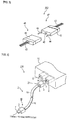
- an HDMI (High-Definition Multimedia Interface (Registered Trademark)) connector 200 shown in Fig. 1 is used to connect a disk reproduction device with a display.
- Fig. 1 is a perspective view illustrating an example of the configuration of the connector 200.
- the connector 200 shown in Fig. 1 adopts a TMDS (Transition Minimized Differential Signaling (Registered Trademark)) transmission method.
- the TMDS (Registered Trademark) transmission method has four channels.
- the connector 200 includes a terminal 40 and a copper cable 41.
- the connector 200 transmits video signals through the copper cable 41 with the terminal 40 inserted into a socket of the HDMI (Registered Trademark), which is not shown.
- Fig. 2 is a schematic diagram illustrating an example of the configuration of the connector 200.
- the terminal 40 of the connector 200 has Pin 1 to Pin 19.
- the Pin 1 to Pin 9 are for an RGB (red, green and blue) video signal connection.
- the Pin 10 to Pin 12 are for a synchronization clock frequency connection.
- the Pin 13 to Pin 19 are for a power supply connection, a control system connection, etc.
- the connector 200 electrically outputs R, G and B video signals input from the Pin 1 to Pin 9 through the copper cable 41.
- An optical fiber connector is broadly divided into two types: a single core type having one optical fiber and a multi-core type having a plurality of optical fibers.
- Single core plugs are widespread mainly for consumer use because of its easy connection and high dust tolerance.
- a data transfer rate is low due to being a single core, which may lead to a problem when high-capacity high-resolution videos are handled.
- FIG. 3 is a perspective view illustrating an example of the configuration of a multi-core MT connector 300.
- the MT connector 300 shown in Fig. 3 includes a plug section 47 and a connector section 48.
- the plug section 47 has a plug body 42, an optical fiber tape 43, a guide pin 44 and an optical fiber end portion 45.
- the optical fiber tape 43 extends from the rear end of the plug body 42.
- Two guide pins 44 protrude from the front end of the plug body 42.
- the optical fiber end portion 45 is provided on the front end of the plug body 42. An optical signal is input to/output from the optical fiber end portion 45.
- the connector section 48 has a connector body 46, an optical fiber tape 43 and an optical fiber end portion (not shown).
- the optical fiber tape 43 extends from the rear end of the connector body 46.
- the optical fiber end portion (not shown) is provided on the front end of the connector body 46. An optical signal is input to/output from the optical fiber end portion.
- the guide pin 44 of the plug section 47 is inserted into the insertion portion (not shown) in the connector section 48, and the plug section 47 and the connector section 48 are secured by a given fastener.
- the optical fiber end portion 45 of the plug section 47 is aligned with the optical fiber end portion (not shown) of the connector section 48. Since an accuracy of the alignment of the optical fiber end portions must be 1 ⁇ m or less, a dedicated attaching/detaching tool is required (e.g., Fig. 1 in JP-A-2004-317737 ).
- the terminal 40 has 19 pins from Pin 1 to Pin 19. Therefore, when the terminal 40 is inserted into a given connector, in a case where the terminal 40 is inserted accidentally slightly slanted with respect to the connector, the 19 pins may not match the insertion holes of the connector, and the pins may be bent and broken.
- the present invention solves such problems, and it is an object of the present invention to provide a connector system, a connecting cable and a receiving tool allowing a connecting tool to be easily attached to/detached from a receiving tool without breaking a terminal due to contact such as in a case where a conventional contact type terminal is used.
- a connector system includes a receiving tool provided on a device, and a connecting tool connected to the receiving tool in a freely attachable/detachable manner so as to establish a connection between devices, the receiving tool having a first wireless communication section that performs wireless communication, the connecting tool having at a position opposite to the first wireless communication section of the receiving tool a second wireless communication section that performs wireless communication with the first wireless communication section.
- the receiving tool (connector) provided on a device has a first wireless communication section that performs wireless communication.
- the connecting tool (plug) connected to the receiving tool in a freely attachable/detachable manner has a second wireless communication section at a position opposite to the first wireless communication section of the receiving tool.
- the connecting tool is inserted and fit into the receiving tool in a given direction, and the first wireless communication section and the second wireless communication section are positioned so that the given insertion direction is orthogonal to the direction normal to the output surface of a wireless signal emitted by the first and second wireless communication sections.
- the connecting tool when the connecting tool is connected to the receiving tool, the second wireless communication section of the connecting tool and the first wireless communication section of the receiving tool can wirelessly communicate with each other in a non-contact state.
- the connecting tool can be easily attached to/detached from the receiving tool without breaking a terminal due to contact such as in a case where a conventional contact type terminal is used.
- a connecting cable includes a cable for transmitting a signal, a first connecting tool attached to one end of the cable, and a second connecting tool attached to the other end of the cable, at least one of the first and second connecting tools being connected in a freely attachable/detachable manner to a receiving tool of a device provided with the receiving tool having a first wireless communication section that performs wireless communication, and having at a position opposite to the first wireless communication section of the receiving tool a second wireless communication section that performs wireless communication with the first wireless communication section.
- the connecting cable according to the present invention is applied when establishing a connection between devices, at least one of which is provided with the receiving tool having the first wireless communication section that performs wireless communication. At least one of the first and second connecting tools of the connecting cable has a second wireless communication section at a position opposite to the first wireless communication section of the receiving tool.
- the second wireless communication section of the connecting tool and the first wireless communication section of the receiving tool can wirelessly communicate with each other in a non-contact state.
- a receiving tool connects in a freely attachable/detachable manner to a connecting tool having a second wireless communication section that performs wireless communication, and has at a position opposite to the second wireless communication section of the connecting tool a first wireless communication section that performs wireless communication with the second wireless communication section.
- the receiving tool according to the present invention is applied to a device to which the connecting tool having the second wireless communication section that performs wireless communication is connected.
- the receiving tool has the first wireless communication section at a position opposite to the second wireless communication section of the connecting tool, which is connected thereto in a freely attachable/detachable manner.
- the first wireless communication section of the receiving tool and the second wireless communication section of the connecting tool can wirelessly communicate with each other in a non-contact state.
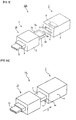
- FIG. 4 An example of the configuration of an attachable/detachable connector system 100 will be described with reference to Fig. 4 .
- the attachable/detachable connector system 100 shown in Fig. 4 is used to connect a video reproducer such as a DVD recorder (not shown) with a video output device such as a projector 21.
- the attachable/detachable connector system 100 includes a connecting cable 1 and a connector 2 (an example of a receiving tool). One end of the connecting cable 1 is fit into the connector 2 of the projector 21, and the other end of the connecting cable 1 is fit into the connector 2 of the video reproducer. A video/audio signal reproduced by the video reproducer is output to the projector 21 through the connecting cable 1.
- the connecting cable 1 includes plugs 1A and 1B and a combined electrical and optical cable 10.
- the plug 1A is an example of a connecting tool, and is connected to the connector 2 in a freely attachable/detachable manner.
- the plug 1A includes a plug body 3, a protruding section 7 and a cable support section 9.
- the protruding section 7 is provided on the front end of the rectangular parallelepiped plug body 3, and the cable support section 9 is provided on the rear end of the plug body 3.
- a first RF (Radio Frequency) chip 5A shown in Fig. 5 is provided in the protruding section 7.
- the protruding section 7 is inserted into an aperture section 8 in the connector 2 of the projector 21, for example.
- the cable support section 9 extends and supports the combined electrical and optical cable 10 (an example of a cable).
- the plug 1B is provided on the end portion of the extended combined electrical and optical cable 10. Since the plugs 1B and 1A have the identical configuration, the description of the configuration of the plug 1B is omitted.
- An RF chip 5A of the plug 1A shown in Fig. 5 serves as an example of a second wireless communication section, and is provided at a portion opposite to an RF chip 6 of the connector 2 so as to perform wireless communication.
- the main surface 5a (output surface of an RF signal) of the RF chip 5A of the plug 1A is sealed with a resin or the like so that the RF chip 5A is not exposed. This allows the RF chip 5A to be protected against stress at the time of attachment/detachment and the effects of temperature and moisture.
- the aperture section 8 of the connector 2 is open to a size that allows the protruding section 7 of the plug 1A to be inserted.
- a second RF chip 6 is provided on the top of the aperture section 8.
- the RF chip 6 serves as an example of a first wireless communication section, and is provided at a position opposite to the RF chip 5A of the plug 1A so as to perform wireless communication.
- a main surface 6a (output surface of an RF signal) of the RF chip 6 is sealed with a resin or the like so that the RF chip 6 is not exposed.
- the RF chip 5A and the RF chip 6 are positioned so that, when the protruding section 7 of the plug 1A is inserted and fit into the aperture section 8 of the connector 2, the RF chip 5A provided in the protruding section 7 is opposite to the RF chip 6 provided on the top of the aperture section 8.
- Hemispherical recessed portions 11 are provided on both sides of the aperture section 8 of the connector 2.
- Each hemispherical protruding portion 12 on the plug 1A shown in Fig. 7A is engaged with each recessed portion 11 when the plug 1A is fit into the connector 2. This can prevent the plug 1A from slipping out of the connector 2, as well as allowing the positions of the RF chip 5A of the plug 1A and the RF chip 6 of the connector 2 to be defined precisely.
- a method of fixing the plug 1A to the connector 2 is not limited to the above-described method, and other methods may be used.
- the RF chip 5A of the plug 1A receives an optical signal propagating through the combined electrical and optical cable 10, converts the optical signal into an electric signal (RF signal), and transmits the electric signal to the RF chip 6 of the connector 2.
- the RF chip 6 of the connector 2 receives the electric signal (RF signal) transmitted from the plug 1A, and outputs the signal to a subsequent-stage processing section, which performs processing such as amplification.
- the RF chip 5A receives the electric signal (RF signal) transmitted by the RF chip 6 of the connector 2, converts the signal into an optical signal, and emits the optical signal to the combined electrical and optical cable 10.
- the RF chip 5A of the plug 1A and the RF chip 6 of the connector 2 can perform data communication in a non-contact state. This allows the plug 1A to be easily attached to/detached from the connector 2 without breaking the RF chips 5A and 6.
- FIG. 6A An example of the fitting of the plug 1A will be described with reference to Figs. 6A and 6B .
- the front end of the protruding section 7 of the plug 1A is inserted into the aperture section 8 in the connector 2.
- the plug 1A is pushed and slid in the direction of an arrow P.
- each protruding portion 12 on the plug 1A (see Fig. 7A ) abuts against a front face 4a of the connector 2.
- the plug 1A shown in Fig. 7A has hemispherical protruding portions 12 on both sides near the root of the protruding section 7. These protruding portions 12 snap into the recessed portions 11 on the plug 1A as described in connection with Fig. 5 .
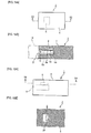
- Fig. 7B is a cross sectional view in the X1-X1 arrow direction illustrating the plug 1A of FIG. 7A .
- the main surface 5a (output surface of an RF signal) of the RF chip 5A of the plug 1A shown in Fig. 7B is sealed with a resin or the like and provided in the protruding section 7.
- the RF chip 5A of the plug 1A is positioned so that the upper surface 7a of the protruding section 7 is orthogonal to the direction normal to the main surface 5a of the RF chip 5A.
- the RF chip 5A is connected to the combined electrical and optical cable 10.
- An optical fiber 18 of the combined electrical and optical cable 10 is covered with a coating member 19 such as a resin.
- the RF chip 5A receives an optical signal propagating through the optical fiber 18, which is an example of an optical transmission path, converts the optical signal into an electric signal (RF signal), and transmits the electric signal in the direction normal to the main surface 5a. Further, the RF chip 5A receives the electric signal (RF signal) transmitted by the RF chip 6 of the connector 2 in the direction normal to the main surface 5a, converts the signal into an optical signal, and emits the optical signal to the optical fiber 18.
- Fig. 8B is a cross sectional view in the X2-X2 arrow direction illustrating the plug 1A of FIG. 8A .
- the RF chip 5A of the plug 1A shown in Fig. 8B includes an antenna section 13, an amplifier 14, a light receiving section 15, an optical modulator 16 and an LD (Laser Diode) 17.
- the antenna section 13 has directivity, and receives/transmits RF signals in a particular direction.
- the amplifier 14 connected to the antenna section 13 and optical modulator 16 amplifies the electric signal output from the antenna section 13 and outputs the signal to the optical modulator 16.
- the optical modulator 16 is connected to the LD 17 and the optical fiber 18, and modulates the optical signal received from the LD 17 based on the amplified electric signal.
- the optical modulator 16 emits the modulated optical signal to the optical fiber 18.
- power is supplied to the LD 17 through a contact terminal No. 18 (see Fig. 9 ).
- the LD 17 is connected to a light supply cable 20, and emits an optical signal to the light supply cable 20.
- the plug 1B shown in Fig. 4 receives the optical signal from the light supply cable 20, and modulates the optical signal based on a predetermined electric signal.
- the light receiving section 15 receives the optical signal from the optical fiber 18.
- the light receiving section 15 is connected to the amplifier 14, converts the received optical signal into an electric signal, and outputs the electric signal to the amplifier 14.
- the amplifier 14 amplifies and outputs the electric signal to the antenna section 13.
- the antenna section 13 emits the electric signal as an RF signal.
- the RF chip 5A shown in Fig. 9 functionally corresponds to the HDMI (Registered Trademark) connector 200 according to a conventional example shown in Figs. 1 and 2 , for example.
- the RF chip 5A has four channels in total: optical fibers 18 for data transmission (channels CH1 to CH3) and an optical fiber 18 for clock transmission (channel CH4).
- the RF chip 5A has contact terminals No. 13 to No. 19 corresponding to the Pin 13 to Pin 19 in the HDMI (Registered Trademark) connector 200 shown in Fig. 2 .
- Each of these contact terminals No. 13 to No. 19 is connected to each power supply signal cable 23. Since the function of the contact terminals No. 13 to No. 19 is well known, it is not described.
- the antenna section 13 includes four RX (receiving) antennas 13a and four TX (transmitting) antennas 13b.
- the arrangement pitch between RX antennas 13a is about 1 mm at most.
- the arrangement pitch between TX antennas 13b is also about 1 mm at most.
- the RX antennas 13a receive RF signals.
- the TX antennas 13b emit RF signals.
- the power supply to the RX antennas 13a and the TX antennas 13b is restricted in order to prevent interference (crosstalk).
- a power supply section 54 connected to the contact terminal No. 18 of the RF chip 6 of the connector 2 shown in Fig. 16 restricts the power supplied to the RX antennas 13a and the TX antennas 13b of the RF chip 5A of the plug 1A.
- the contact terminal No. 18 of the RF chip 5A shown in Fig. 9 and the contact terminal No. 18 of the RF chip 6 shown in Fig. 16 are connected to each other.
- a predetermined voltage is applied from the power supply section 54 to the contact terminal No. 18 of the RF chip 6 shown in Fig. 16 .
- a predetermined power is supplied to the contact terminal No. 18 of the RF chip 5A shown in Fig. 9 , which is connected to the contact terminal No. 18 of the RF chip 6 shown in Fig. 16 .
- a predetermined power is supplied to the RX antennas 13a and the TX antennas 13b of the RF chip 5A.
- the RX antennas 13a and the TX antennas 13b are positioned by changing the plane of polarization of the RX antennas 13a adjacent to each other and the TX antennas 13b adjacent to each other in order to prevent interference.
- the adjacent RX antennas 13a, 13a are positioned to have circularly polarized waves in different directions of rotation (left-hand circular polarization and right-hand circular polarization) so that the planes of polarization of them are orthogonal to each other.
- the crosstalk (interference) between the RX antennas 13a, 13a adjacent to each other can be suppressed.
- the amplifier 14 includes eight AMPs 14a. Each AMP 14a is connected to each RX antenna 13a and TX antenna 13b. The AMP 14a amplifies an electric signal input from the RX antenna 13a. In addition, the AMP 14a amplifies the electric signal input from the light receiving section 15, and outputs the signal to the TX antenna 13b.
- the light receiving section 15 includes four light receiving elements (O-R) 15a. These light receiving elements 15a serve as an example of an optical-electric conversion section, are connected to the optical fibers 18 of the channels CH1 to CH4 through optical waveguides 22, and further connected to the TX antennas 13b through the AMPs 14a.
- the light receiving element 15a receives an optical signal propagating through the optical fiber 18, converts the signal into an electric signal, and outputs the electric signal to the TX antenna 13b through the AMP 14a.
- the optical modulator 16 includes four light modulators (E-O) 16a. These light modulators 16a serve as an example of an electric-optical conversion section, are connected to the RX antennas 13a through the AMPs 14a, and further connected to the LD 17 and the optical fibers 18 of the channels CH1 to CH4.
- the optical modulator 16a converts an electric signal into an optical signal. For example, the optical modulator 16a modulates an optical signal received from the LD 17 based on the electric signal input from the X antenna 13a through the AMP 14a.
- the optical modulator 16a emits the modulated optical signal to the optical fibers 18 of the channels CH1 to CH4.
- the RX antenna 13a shown in Fig. 9 receives an RF signal
- the RX antenna 13a converts the RF signal into a predetermined electric signal, and outputs the electric signal to the AMP 14a.
- the AMP 14a amplifies the electric signal output from the RX antenna 13a, and outputs the signal to the optical modulator (E-O) 16a.
- the optical modulator 16a modulates the optical signal received from the LD 17 based on the amplified electric signal, and emits the modulated optical signal to the optical fibers 18 of the channels CH1 to CH4.
- the light receiving element 15a receives the optical signal from the optical fiber 18.
- the light receiving element 15a converts the received optical signal into an electric signal and outputs the electric signal to the AMP 14a.
- the AMP 14a amplifies and outputs the electric signal to the TX antenna 13b.
- the TX antenna 13b emits the amplified electric signal as an RF signal.
- the RF chip 5B shown in Fig. 10 receives a light source from the light supply cable 20, the RF chip 5B does not have the LD 17 shown in Fig. 9 .
- Like components of the RF chip 5B are denoted by like numerals as of the RF chip 5A, and the description thereof is omitted.
- the RF chip 5B has four channels in total: optical fibers 18 for data transmission (channels CH1 to CH3) and an optical fiber 18 for clock transmission (channel CH4).
- the optical fibers 18 of these channels CH1 to CH4 are connected to the optical fibers 18 of the CH1 to CH4 shown in Fig. 9 .
- the RF. chip 5B has contact terminals No. 13 to No. 19 corresponding to the Pin 13 to Pin 19 in the HDMI (Registered Trademark) connector 200 shown in Fig. 2 .
- Each of these contact terminals No. 13 to No. 19 is connected to each power supply signal cable 23.
- Each power supply signal cable 23 is connected to each power supply signal cable 23 shown in Fig. 9 .
- the antenna section 13 includes four RX (receiving) antennas 13a and four TX (transmitting) antennas 13b.
- the RX antennas 13a receive RF signals.
- the TX antennas 13b emit RF signals.
- the amplifier 14 includes eight AMPs 14a. Each AMP 14a is connected to each RX antenna 13a and TX antenna 13b. The AMP 14a amplifies an electric signal input from the RX antenna 13a. In addition, the AMP 14a amplifies the electric signal input from the light receiving section 15, and outputs the signal to the TX antenna 13b.
- the light receiving section 15 includes four light receiving elements (O-E) 15a. These light receiving elements 15a are connected to the optical fibers 18 of the channels CH1 to CH4 through the optical waveguides 22, and further, connected to the TX antennas 13b through the AMPs 14a. The light receiving element 15a converts an optical signal propagating through the optical fiber 18 into an electric signal, and outputs the electric signal to the TX antenna 13b through the AMP 14a.
- O-E light receiving elements
- the optical modulator 16 includes four light modulators (E-O) 16a. These light modulators 16a are connected to the RX antennas 13a through the AMPs 14a, and further connected to the light supply cable 20 and the optical fibers 18 of the channels CH1 to CH4. The optical modulator 16a modulates an optical signal received from the light supply cable 20 based on the electric signal input from the RX antenna 13a through the AMP 14a. The optical modulator 16a emits the modulated optical signal to the optical fibers 18 of the channels CH1 to CH4.
- E-O light modulators
- the RX antenna 13a shown in Fig. 10 receives an RF signal
- the RX antenna 13a converts the RF signal into a predetermined electric signal, and outputs the electric signal to the AMP 14a.
- the AMP 14a amplifies the electric signal-output from the RX antenna 13a, and outputs the signal to the optical modulator (E-O) 16a.
- the optical modulator 16a modulates the optical signal received from the LD 17 shown in Fig. 9 through the light supply cable 20 based on the amplified electric signal, and emits the modulated optical signal to the optical fibers 18 of the channels CH1 to CH4.
- the light receiving element 15a receives the optical signal from the optical fiber 18.
- the light receiving element 15a converts the received optical signal into an electric signal and outputs the electric signal to the AMP 14a.
- the AMP 14a amplifies and outputs the electric signal to the TX antenna 13b.
- the TX antenna 13b emits the amplified electric signal as an RF signal.
- the LD 17 shown in Fig. 9 may also be mounted on the RF chip 5B shown in Fig. 10 . In this case, the light supply cable 20 is not required for the RF chip 5A and the RF chip 5B.
- discrete components such as a light source and a detector (not shown) (light receiving element 15a and optical modulator 16a) may be positioned on each optical fiber 18.
- the RX antennas 13a, the TX antennas 13b, the AMPs 14a and the contact terminals No. 13 to No. 19 are positioned on the chassis 49 of the RF chip 5C.
- the light receiving element (O-E) 15a and the optical modulator (E-O) 16a are not positioned on the chassis 49 of the RF chip 5C.
- the optical signal transmission direction is unidirectional, it may also be a bidirectional communication.
- the bidirectional communication is easily achieved using a branching optical waveguide 50 as shown in Fig. 12 .
- the RF chip 5D shown in Fig. 12 only components related to the channel CH1 are shown, and components related to the other channels CH2 to CH4 and the contact terminals No. 13 to No. 19 are omitted.
- the channel CH1 shown in Fig. 12 is constituted by one optical fiber 18.
- the optical fiber 18 is connected to the light receiving element 15a and the optical modulator 16a through the branching optical waveguide 50.
- the branching optical waveguide 50 transmits an optical signal output from the optical modulator 16a to the optical fiber 18.
- the branching optical waveguide 50 transmits the optical signal propagating from the optical fiber 18 to the light receiving element 15a.
- the manufacturing process of the RF chip 5A of the plug 1A will be described with reference to Figs. 13A and 13B .
- the entire surface of the chassis 49 (substrate) of the RF chip 5A shown in Fig. 13A is lined with a copper foil.
- a pattern is printed and etched on the chassis 49.
- the remaining photo-sensitive film is striped to expose the copper foil pattern.
- resist ink having insulation action is applied over the chassis 49, and is dried and developed to expose a circuit and the contact terminals No. 13 to No. 19.
- the material of the chassis 49 is a silicone resin, for example.
- an alignment groove 53 for optical fiber shown in Fig. 13A nine predetermined positions on the chassis 49 are cut in rectangles with a substrate processing machine.
- the alignment groove 53 is not limited to a rectangular shape, and may have a V-shape.
- the optical waveguide 22 is mounted by adhesion to the predetermined portion with an adhesive agent.
- the antenna section 13, the amplifier 14, the light receiving element 15a, and the optical modulator 16a are mounted on predetermined positions on the chassis 49. Subsequently, as shown in Fig.
- the LD 17 is mounted on a predetermined position on the chassis 49, and each optical fiber 18 and the light supply cable 20 are mounted by adhesion to the alignment groove 53 with an adhesive agent. At that time, the cores of the optical fiber 18 and the light supply cable 20 are mounted by alignment with the core of the optical waveguide 22.
- Fig. 14B is a cross sectional view in the X3-X3 arrow direction of FIG. 14A illustrating the example of the configuration of the connector 2.
- the plug 1A fit into the connector 2 is shown in a chain double-dashed line.
- the main surface 6a (output surface of an RF signal) of the RF chip 6 of the connector 2 shown in Fig. 14B is sealed with a resin or the like and provided in the connector body 4.
- the RF chip 6 is positioned so that the upper surface 8a of the aperture section 8 is orthogonal to the direction normal to the main surface 6a of the RF chip 6.
- the RF chip 5A and the RF chip 6 are positioned so that the direction of insertion of the plug 1A into the connector 2 is orthogonal to the direction normal to the output surface of the RF signal emitted from the RF chip 5A of the plug 1A and the RF chip 6 of the connector 2.
- the main surface 6a of the RF chip 6 of the connector 2 is parallel with the main surface 5a of the RF chip 5A of the plug 1A inserted into the aperture section 8 of the connector 2. Accordingly, the RF signal emitted from the main surface 5a of the RF chip 5A accurately reaches the main surface 6a of the RF chip 6.
- the RF signal emitted from the main surface 6a of the RF chip 6 accurately reaches the main surface 5a of the RF chip 5A.
- the RF chip 6 of the connector 2 is connected to a signal processing section 51 of the projector 21 shown in Fig. 16 .
- the RF chip 6 receives an RF signal from the plug 1A, converts the RF signal into an electric signal, and outputs the electric signal to the signal processing section 51.
- the RF chip 6 converts an electric signal output from an RF circuit 52 shown in Fig. 16 into an RF signal, and emits the RF signal.
- Fig. 15B is a cross sectional view in the X4-X4 arrow direction illustrating the connector 2 of FIG. 15A .
- the RF chip 6 of the connector 2 shown in Fig. 15B includes an antenna section 24.
- the antenna section 24 has directivity, and receives/transmits RF signals in a particular direction.
- the antenna section 24 When the antenna section 24 receives an RF signal, the antenna section 24 converts the RF signal into a predetermined electric signal, and outputs the electric signal to the signal processing section 51 shown in Fig. 16 .
- the signal processing section 51 performs predetermined signal processing such as amplification on the output electric signal.
- the antenna section 24 is connected to an RF circuit 52 shown in Fig. 16 , and emits the electric signal output from the RF circuit 52 as an RF signal.
- the RF chip 6 shown in Fig. 16 includes the antenna section 24.
- the antenna section 24 includes four RX (receiving) antennas 24a and four TX (transmitting) antennas 24b.
- the RX antenna 24a is connected to the signal processing section 51, and converts a received RF signal into an electric signal, and outputs the electric signal to the signal processing section 51.
- the TX antenna 24b is connected to the RF circuit 52, and emits the electric signal input from the RF circuit 52 as an RF signal.
- the RF circuit 52 includes an LNA (Low Noise Amplifier) 52a, a Mixer 52b, an oscillator 52c and a filter 52d.
- the LNA 52a amplifies an input predetermined electric signal and outputs the electric signal to the Mixer 52b.
- the Mixer 52b is connected to the LNA 52a and the oscillator 52c.
- the oscillator 52c oscillates a frequency of 60 GHz, for example.
- the Mixer 52b synthesizes (modulates) the 60 GHz frequency signal and the electric signal amplified by the ULNA 52a, and outputs the synthesized electric signal to the filter 52d.
- the filter 52d serves as a highpass filter, for example, and removes a low-frequency component from the output electric signal.
- the filter 52d outputs to each TX antenna 24b the electric signal from which the low-frequency component was removed.
- the TX antenna 24b emits the output electric signal as an RF signal.
- the frequency of the RF signal is at 60 GHz.
- the first reason is that the RF circuit 52 can be formed on a silicon substrate. Since the actual value of a gain-bandwidth product (ft) of a 90 nm node MOS transistor is about 140 GHz, the configuration supporting 60 GHz is possible as far as a mass-production technique is concerned.
- the second reason is that an antenna can be miniaturized.
- the third reason is that the frequency of 60 GHz is in a band region where electric-optical conversion is possible using a micro ring modulator.
- the fourth reason is that if the carrier is at 60 GHz, the capacity of transmission at about 10 Gbps can be secured. When a transport rate is-low, a carrier of 40 GHz, 25 GHz or the like may be used. In this case, semiconductor components can be created at a lower price.
- the connector 2 provided on the projector 21 has the RF chip 6, and the plug 1A connected to the connector 2 has the RF chip 5A at a position opposite to the RF chip 6 of the connector 2.
- the RF chip 5A of the plug 1A and the RF chip 6 of the connector 2 can perform wireless communication with each other in a non-contact state.
- the plug 1A can be easily attached to/detached from the connector 2 without breaking a terminal due to contact such as in a case where the conventional contact type terminal is used.
- the connector 200 (e.g., version 1.3) shown in Fig. 1
- the electric signal is attenuated with increasing data transmission distance. Therefore, transmitting data over long distances (about 20 mm) is difficult, and for example, hardwiring to a projector installed on a ceiling is not straightforward.
- the attachable/detachable connector system 100 can prevent the attenuation of the data because the optical fiber 18 transmits the data, thus long-distance transmission is possible. Therefore, even at a location such as the projector 21 installed on the ceiling, the attachable/detachable connector system 100 can be used.
- a low cost device can be realized by forming with silicon all the components other than light emitting components.
- the present invention is suitably applied to a connector cable that connects a video reproducer and a display.
Landscapes
- Physics & Mathematics (AREA)
- General Physics & Mathematics (AREA)
- Optics & Photonics (AREA)
- Electromagnetism (AREA)
- Engineering & Computer Science (AREA)
- Computer Networks & Wireless Communication (AREA)
- Signal Processing (AREA)
- Optical Couplings Of Light Guides (AREA)
- Details Of Television Systems (AREA)
- Details Of Connecting Devices For Male And Female Coupling (AREA)
- Telephone Set Structure (AREA)
Abstract
Description
- The present invention relates to a connector system, a connecting cable and a receiving tool applicable to a connector cable connecting a video reproducer and a display. More specifically, a receiving tool provided on a device has a first wireless communication section. A connecting tool connected to the receiving tool in a freely attachable/detachable manner has a second wireless communication section at a position opposite to the first wireless communication section of the receiving tool. Thus, wireless communication can be performed in a non-contact state, and the connecting tool can be easily attached to/detached from the receiving tool without breaking a terminal due to contact such as in a case where a conventional contact type terminal is used.
- In recent years, owing to next-generation large capacity optical disks such as the Blue-ray Disc (Registered Trademark) and high-vision broadcasting, there are increasing cases where a high-resolution video is to be handled. In this case, an HDMI (High-Definition Multimedia Interface (Registered Trademark))
connector 200 shown inFig. 1 is used to connect a disk reproduction device with a display.Fig. 1 is a perspective view illustrating an example of the configuration of theconnector 200. Theconnector 200 shown inFig. 1 adopts a TMDS (Transition Minimized Differential Signaling (Registered Trademark)) transmission method. The TMDS (Registered Trademark) transmission method has four channels. These four channels are assigned to R, G and B (red, green and blue) video signals, one per each channel, and one channel is assigned to a signal for synchronizing a clock frequency. Theconnector 200 includes aterminal 40 and acopper cable 41. Theconnector 200 transmits video signals through thecopper cable 41 with theterminal 40 inserted into a socket of the HDMI (Registered Trademark), which is not shown. -
Fig. 2 is a schematic diagram illustrating an example of the configuration of theconnector 200. Theterminal 40 of theconnector 200 hasPin 1 toPin 19. ThePin 1 toPin 9 are for an RGB (red, green and blue) video signal connection. ThePin 10 toPin 12 are for a synchronization clock frequency connection. ThePin 13 toPin 19 are for a power supply connection, a control system connection, etc, Theconnector 200 electrically outputs R, G and B video signals input from thePin 1 toPin 9 through thecopper cable 41. - In contrast to the
copper cable 41, a connector using an optical fiber in a signal transmission path has also been proposed. An optical fiber connector is broadly divided into two types: a single core type having one optical fiber and a multi-core type having a plurality of optical fibers. Single core plugs are widespread mainly for consumer use because of its easy connection and high dust tolerance. However, a data transfer rate is low due to being a single core, which may lead to a problem when high-capacity high-resolution videos are handled. - On the other hand, although the connection is difficult due to being a multi-core, because a data transfer rate is high and high-capacity high-resolution videos can be handled, multi-core plugs are widespread mainly for industrial use.
Fig. 3 is a perspective view illustrating an example of the configuration of amulti-core MT connector 300. TheMT connector 300 shown inFig. 3 includes a plug section 47 and aconnector section 48. - The plug section 47 has a
plug body 42, anoptical fiber tape 43, aguide pin 44 and an opticalfiber end portion 45. Theoptical fiber tape 43 extends from the rear end of theplug body 42. Twoguide pins 44 protrude from the front end of theplug body 42. The opticalfiber end portion 45 is provided on the front end of theplug body 42. An optical signal is input to/output from the opticalfiber end portion 45. - The
connector section 48 has aconnector body 46, anoptical fiber tape 43 and an optical fiber end portion (not shown). Theoptical fiber tape 43 extends from the rear end of theconnector body 46. The optical fiber end portion (not shown) is provided on the front end of theconnector body 46. An optical signal is input to/output from the optical fiber end portion. - When the plug section 47 is connected with the
connector section 48, theguide pin 44 of the plug section 47 is inserted into the insertion portion (not shown) in theconnector section 48, and the plug section 47 and theconnector section 48 are secured by a given fastener. At that time, the opticalfiber end portion 45 of the plug section 47 is aligned with the optical fiber end portion (not shown) of theconnector section 48. Since an accuracy of the alignment of the optical fiber end portions must be 1 µm or less, a dedicated attaching/detaching tool is required (e.g.,Fig. 1 inJP-A-2004-317737 - According to the HDMI (Registered Trademark)
connector 200 shown inFigs. 1 and 2 , theterminal 40 has 19 pins fromPin 1 toPin 19. Therefore, when theterminal 40 is inserted into a given connector, in a case where theterminal 40 is inserted accidentally slightly slanted with respect to the connector, the 19 pins may not match the insertion holes of the connector, and the pins may be bent and broken. - In addition, according to the
MT connector 300 shown inFig. 3 , since an accuracy of the alignment of the opticalfiber end portion 45 of the plug section 47 with the optical fiber end portion (not shown) of theconnector section 48 must be 1 µm or less, which requires a dedicated attaching/detaching tool for industrial use, employment for consumer use is difficult. - Accordingly, the present invention solves such problems, and it is an object of the present invention to provide a connector system, a connecting cable and a receiving tool allowing a connecting tool to be easily attached to/detached from a receiving tool without breaking a terminal due to contact such as in a case where a conventional contact type terminal is used.
- In order to solve the problems described above, a connector system according to the present invention includes a receiving tool provided on a device, and a connecting tool connected to the receiving tool in a freely attachable/detachable manner so as to establish a connection between devices, the receiving tool having a first wireless communication section that performs wireless communication, the connecting tool having at a position opposite to the first wireless communication section of the receiving tool a second wireless communication section that performs wireless communication with the first wireless communication section.
- According to the connector system of the present invention, the receiving tool (connector) provided on a device has a first wireless communication section that performs wireless communication. The connecting tool (plug) connected to the receiving tool in a freely attachable/detachable manner has a second wireless communication section at a position opposite to the first wireless communication section of the receiving tool. For example, the connecting tool is inserted and fit into the receiving tool in a given direction, and the first wireless communication section and the second wireless communication section are positioned so that the given insertion direction is orthogonal to the direction normal to the output surface of a wireless signal emitted by the first and second wireless communication sections. As a result, when the connecting tool is connected to the receiving tool, the second wireless communication section of the connecting tool and the first wireless communication section of the receiving tool can wirelessly communicate with each other in a non-contact state. Thus, the connecting tool can be easily attached to/detached from the receiving tool without breaking a terminal due to contact such as in a case where a conventional contact type terminal is used.
- In order to solve the problems described above, a connecting cable according to the present invention includes a cable for transmitting a signal, a first connecting tool attached to one end of the cable, and a second connecting tool attached to the other end of the cable, at least one of the first and second connecting tools being connected in a freely attachable/detachable manner to a receiving tool of a device provided with the receiving tool having a first wireless communication section that performs wireless communication, and having at a position opposite to the first wireless communication section of the receiving tool a second wireless communication section that performs wireless communication with the first wireless communication section.
- The connecting cable according to the present invention is applied when establishing a connection between devices, at least one of which is provided with the receiving tool having the first wireless communication section that performs wireless communication. At least one of the first and second connecting tools of the connecting cable has a second wireless communication section at a position opposite to the first wireless communication section of the receiving tool. Thus, the second wireless communication section of the connecting tool and the first wireless communication section of the receiving tool can wirelessly communicate with each other in a non-contact state.
- In order to solve the problems described above, a receiving tool according to the present invention connects in a freely attachable/detachable manner to a connecting tool having a second wireless communication section that performs wireless communication, and has at a position opposite to the second wireless communication section of the connecting tool a first wireless communication section that performs wireless communication with the second wireless communication section.
- The receiving tool according to the present invention is applied to a device to which the connecting tool having the second wireless communication section that performs wireless communication is connected. The receiving tool has the first wireless communication section at a position opposite to the second wireless communication section of the connecting tool, which is connected thereto in a freely attachable/detachable manner. Thus, the first wireless communication section of the receiving tool and the second wireless communication section of the connecting tool can wirelessly communicate with each other in a non-contact state.
-
- [
Fig. 1] Fig. 1 is a perspective view illustrating an example (1) of the configuration of an HDMI (Registered Trademark)connector 200 according to a conventional example. - [
Fig. 2] Fig. 2 is a schematic diagram illustrating an example (2) of the configuration of theconnector 200 according to the conventional example. - [
Fig. 3] Fig. 3 is a perspective view illustrating an example of the configuration of anMT connector 300 according to the conventional example. - [
Fig. 4] Fig. 4 is a perspective view illustrating an example of the configuration of an attachable/detachable connector system 100 according to the present invention. - [
Fig. 5] Fig. 5 is a perspective view illustrating an example of the configuration of aplug 1A and aconnector 2. - [
Fig. 6A] Fig. 6A is a perspective view illustrating an example of the beginning of fitting of theplug 1A. - [
Fig. 6B] Fig. 6B is a perspective view illustrating an example of the completion of fitting of theplug 1A. - [
Fig. 7A] Fig. 7A is a top view illustrating an example of the configuration of theplug 1A. - [
Fig. 7B] Fig. 7B is a cross sectional view in the X1-X1 arrow direction ofFIG. 7A illustrating the example of the configuration of theplug 1A. - [
Fig. 8A] Fig. 8A is a side view illustrating an example of the configuration of theplug 1A. - [
Fig. 8B] Fig. 8B is a cross sectional view in the X2-X2 arrow direction ofFIG. 8A illustrating the example of the configuration of theplug 1A. - [
Fig. 9] Fig. 9 is a block diagram illustrating an example of the configuration of anRF chip 5A of theplug 1A. - [
Fig. 10] Fig. 10 is a block diagram illustrating an example of the configuration of anRF chip 5B of aplug 1B. - [
Fig. 11] Fig. 11 is a block diagram illustrating an example of the configuration of anRF chip 5C of aplug 1C. -
[Fig. 12] Fig. 12 is a block diagram illustrating an example of the configuration of part of anRF chip 5D of aplug 1D. - [
Fig. 13A] Fig. 13A is a perspective view illustrating an example of a first manufacturing process of theRF chip 5A. - [
Fig. 13B] Fig. 13B is a perspective view illustrating an example of a second manufacturing process of theRF chip 5A. - [
Fig. 14A] Fig. 14A is a top view illustrating an example of the configuration of theconnector 2. - [
Fig. 14B] Fig. 14B is a cross sectional view in the X3-X3 arrow direction ofFIG. 14A illustrating the example of the configuration of theconnector 2. - [
Fig. 15A] Fig. 15A is a side view illustrating an example of the configuration of theconnector 2. - [
Fig. 15B] Fig. 15B is a cross sectional view in the X4-X4 arrow direction ofFIG. 15A illustrating the example of the configuration of theconnector 2. - [
Fig. 16] Fig. 16 is a block diagram illustrating an example of the configuration of anRF chip 6 and anRF circuit 52. - An embodiment of a connector system, a connecting cable and a receiving tool according to the present invention will be described below with reference to the drawings.
- An example of the configuration of an attachable/
detachable connector system 100 will be described with reference toFig. 4 . The attachable/detachable connector system 100 shown inFig. 4 is used to connect a video reproducer such as a DVD recorder (not shown) with a video output device such as aprojector 21. - The attachable/
detachable connector system 100 includes a connectingcable 1 and a connector 2 (an example of a receiving tool). One end of the connectingcable 1 is fit into theconnector 2 of theprojector 21, and the other end of the connectingcable 1 is fit into theconnector 2 of the video reproducer. A video/audio signal reproduced by the video reproducer is output to theprojector 21 through the connectingcable 1. - The connecting
cable 1 includesplugs optical cable 10. Theplug 1A is an example of a connecting tool, and is connected to theconnector 2 in a freely attachable/detachable manner. Theplug 1A includes aplug body 3, a protrudingsection 7 and acable support section 9. The protrudingsection 7 is provided on the front end of the rectangularparallelepiped plug body 3, and thecable support section 9 is provided on the rear end of theplug body 3. A first RF (Radio Frequency)chip 5A shown inFig. 5 is provided in the protrudingsection 7. The protrudingsection 7 is inserted into anaperture section 8 in theconnector 2 of theprojector 21, for example. - The
cable support section 9 extends and supports the combined electrical and optical cable 10 (an example of a cable). Theplug 1B is provided on the end portion of the extended combined electrical andoptical cable 10. Since theplugs plug 1B is omitted. - An example of the configuration of the
plug 1A and theconnector 2 will be described with reference toFig. 5 . AnRF chip 5A of theplug 1A shown inFig. 5 serves as an example of a second wireless communication section, and is provided at a portion opposite to anRF chip 6 of theconnector 2 so as to perform wireless communication. Themain surface 5a (output surface of an RF signal) of theRF chip 5A of theplug 1A is sealed with a resin or the like so that theRF chip 5A is not exposed. This allows theRF chip 5A to be protected against stress at the time of attachment/detachment and the effects of temperature and moisture. - The
aperture section 8 of theconnector 2 is open to a size that allows the protrudingsection 7 of theplug 1A to be inserted. Asecond RF chip 6 is provided on the top of theaperture section 8. TheRF chip 6 serves as an example of a first wireless communication section, and is provided at a position opposite to theRF chip 5A of theplug 1A so as to perform wireless communication. In this example, in order to protect theRF chip 6 against the stress at the time of attachment/detachment, amain surface 6a (output surface of an RF signal) of theRF chip 6 is sealed with a resin or the like so that theRF chip 6 is not exposed. - In addition, the
RF chip 5A and theRF chip 6 are positioned so that, when the protrudingsection 7 of theplug 1A is inserted and fit into theaperture section 8 of theconnector 2, theRF chip 5A provided in the protrudingsection 7 is opposite to theRF chip 6 provided on the top of theaperture section 8. - Hemispherical recessed
portions 11 are provided on both sides of theaperture section 8 of theconnector 2. Each hemispherical protrudingportion 12 on theplug 1A shown inFig. 7A is engaged with each recessedportion 11 when theplug 1A is fit into theconnector 2. This can prevent theplug 1A from slipping out of theconnector 2, as well as allowing the positions of theRF chip 5A of theplug 1A and theRF chip 6 of theconnector 2 to be defined precisely. Naturally, a method of fixing theplug 1A to theconnector 2 is not limited to the above-described method, and other methods may be used. - The
RF chip 5A of theplug 1A receives an optical signal propagating through the combined electrical andoptical cable 10, converts the optical signal into an electric signal (RF signal), and transmits the electric signal to theRF chip 6 of theconnector 2. TheRF chip 6 of theconnector 2 receives the electric signal (RF signal) transmitted from theplug 1A, and outputs the signal to a subsequent-stage processing section, which performs processing such as amplification. Further, theRF chip 5A receives the electric signal (RF signal) transmitted by theRF chip 6 of theconnector 2, converts the signal into an optical signal, and emits the optical signal to the combined electrical andoptical cable 10. - In this manner, when the
plug 1A is fit into theconnector 2, theRF chip 5A of theplug 1A and theRF chip 6 of theconnector 2 can perform data communication in a non-contact state. This allows theplug 1A to be easily attached to/detached from theconnector 2 without breaking theRF chips - An example of the fitting of the
plug 1A will be described with reference toFigs. 6A and6B . As shown inFig. 6A , the front end of the protrudingsection 7 of theplug 1A is inserted into theaperture section 8 in theconnector 2. After insertion, theplug 1A is pushed and slid in the direction of an arrow P. When theplug 1A is slid, each protrudingportion 12 on theplug 1A (seeFig. 7A ) abuts against afront face 4a of theconnector 2. After the abutting, when theplug 1A is further pushed in the direction of the arrow P, due to eachabutting protruding portion 12, theconnector body 4 becomes slightly bent such that theaperture section 8 of theconnector 2 widens laterally. With theconnector body 4 bent, when theplug 1A is further pushed and slid in the direction of the arrow P until the position shown inFig. 6B is reached, each protrudingportion 12 on theplug 1A snaps into the recessedportion 11 on the connector 2 (seeFig. 5 ), and the bending is reverted. In this manner, theplug 1A is fit into theconnector 2. - Subsequently, an example of the configuration of the
plug 1A will be described in detail with reference toFigs. 7A to 8B . Theplug 1A shown inFig. 7A has hemispherical protrudingportions 12 on both sides near the root of the protrudingsection 7. These protrudingportions 12 snap into the recessedportions 11 on theplug 1A as described in connection withFig. 5 . -
Fig. 7B is a cross sectional view in the X1-X1 arrow direction illustrating theplug 1A ofFIG. 7A . Themain surface 5a (output surface of an RF signal) of theRF chip 5A of theplug 1A shown inFig. 7B is sealed with a resin or the like and provided in the protrudingsection 7. TheRF chip 5A of theplug 1A is positioned so that theupper surface 7a of the protrudingsection 7 is orthogonal to the direction normal to themain surface 5a of theRF chip 5A. - The
RF chip 5A is connected to the combined electrical andoptical cable 10. Anoptical fiber 18 of the combined electrical andoptical cable 10 is covered with acoating member 19 such as a resin. TheRF chip 5A receives an optical signal propagating through theoptical fiber 18, which is an example of an optical transmission path, converts the optical signal into an electric signal (RF signal), and transmits the electric signal in the direction normal to themain surface 5a. Further, theRF chip 5A receives the electric signal (RF signal) transmitted by theRF chip 6 of theconnector 2 in the direction normal to themain surface 5a, converts the signal into an optical signal, and emits the optical signal to theoptical fiber 18. -
Fig. 8B is a cross sectional view in the X2-X2 arrow direction illustrating theplug 1A ofFIG. 8A . TheRF chip 5A of theplug 1A shown inFig. 8B includes anantenna section 13, anamplifier 14, alight receiving section 15, anoptical modulator 16 and an LD (Laser Diode) 17. Theantenna section 13 has directivity, and receives/transmits RF signals in a particular direction. - When the
antenna section 13 receives an RF signal, theamplifier 14 connected to theantenna section 13 andoptical modulator 16 amplifies the electric signal output from theantenna section 13 and outputs the signal to theoptical modulator 16. Theoptical modulator 16 is connected to theLD 17 and theoptical fiber 18, and modulates the optical signal received from theLD 17 based on the amplified electric signal. Theoptical modulator 16 emits the modulated optical signal to theoptical fiber 18. In this example, power is supplied to theLD 17 through a contact terminal No. 18 (seeFig. 9 ). TheLD 17 is connected to alight supply cable 20, and emits an optical signal to thelight supply cable 20. Theplug 1B shown inFig. 4 receives the optical signal from thelight supply cable 20, and modulates the optical signal based on a predetermined electric signal. - Further, when the optical signal propagates from the
optical fiber 18, thelight receiving section 15 receives the optical signal from theoptical fiber 18. Thelight receiving section 15 is connected to theamplifier 14, converts the received optical signal into an electric signal, and outputs the electric signal to theamplifier 14. Theamplifier 14 amplifies and outputs the electric signal to theantenna section 13. Theantenna section 13 emits the electric signal as an RF signal. - Subsequently, an example of the configuration of the
RF chip 5A of theplug 1A will be described with reference toFig. 9 . TheRF chip 5A shown inFig. 9 functionally corresponds to the HDMI (Registered Trademark)connector 200 according to a conventional example shown inFigs. 1 and 2 , for example. Namely, theRF chip 5A has four channels in total:optical fibers 18 for data transmission (channels CH1 to CH3) and anoptical fiber 18 for clock transmission (channel CH4). In addition, theRF chip 5A has contact terminals No. 13 to No. 19 corresponding to thePin 13 to Pin 19 in the HDMI (Registered Trademark)connector 200 shown inFig. 2 . Each of these contact terminals No. 13 to No. 19 is connected to each powersupply signal cable 23. Since the function of the contact terminals No. 13 to No. 19 is well known, it is not described. - The
antenna section 13 includes four RX (receiving)antennas 13a and four TX (transmitting)antennas 13b. In order to realize miniaturization, the arrangement pitch betweenRX antennas 13a is about 1 mm at most. In order to realize miniaturization, the arrangement pitch betweenTX antennas 13b is also about 1 mm at most. TheRX antennas 13a receive RF signals. TheTX antennas 13b emit RF signals. - In this example, when a plurality of the
RX antenna 13a and theTX antenna 13b combinations are to be positioned, the power supply to theRX antennas 13a and theTX antennas 13b is restricted in order to prevent interference (crosstalk). For example, apower supply section 54 connected to the contact terminal No. 18 of theRF chip 6 of theconnector 2 shown inFig. 16 restricts the power supplied to theRX antennas 13a and theTX antennas 13b of theRF chip 5A of theplug 1A. In this example, the contact terminal No. 18 of theRF chip 5A shown inFig. 9 and the contact terminal No. 18 of theRF chip 6 shown inFig. 16 are connected to each other. A predetermined voltage is applied from thepower supply section 54 to the contact terminal No. 18 of theRF chip 6 shown inFig. 16 . At that time, a predetermined power is supplied to the contact terminal No. 18 of theRF chip 5A shown inFig. 9 , which is connected to the contact terminal No. 18 of theRF chip 6 shown inFig. 16 . In addition, a predetermined power is supplied to theRX antennas 13a and theTX antennas 13b of theRF chip 5A. - Furthermore, when a plurality of the
RX antenna 13a and theTX antenna 13b combinations are to be positioned, theRX antennas 13a and theTX antennas 13b are positioned by changing the plane of polarization of theRX antennas 13a adjacent to each other and theTX antennas 13b adjacent to each other in order to prevent interference. For example, theadjacent RX antennas RX antennas - The
amplifier 14 includes eightAMPs 14a. EachAMP 14a is connected to eachRX antenna 13a andTX antenna 13b. TheAMP 14a amplifies an electric signal input from theRX antenna 13a. In addition, theAMP 14a amplifies the electric signal input from thelight receiving section 15, and outputs the signal to theTX antenna 13b. - The
light receiving section 15 includes four light receiving elements (O-R) 15a. Theselight receiving elements 15a serve as an example of an optical-electric conversion section, are connected to theoptical fibers 18 of the channels CH1 to CH4 throughoptical waveguides 22, and further connected to theTX antennas 13b through theAMPs 14a. Thelight receiving element 15a receives an optical signal propagating through theoptical fiber 18, converts the signal into an electric signal, and outputs the electric signal to theTX antenna 13b through theAMP 14a. - The
optical modulator 16 includes four light modulators (E-O) 16a. Theselight modulators 16a serve as an example of an electric-optical conversion section, are connected to theRX antennas 13a through theAMPs 14a, and further connected to theLD 17 and theoptical fibers 18 of the channels CH1 to CH4. Theoptical modulator 16a converts an electric signal into an optical signal. For example, theoptical modulator 16a modulates an optical signal received from theLD 17 based on the electric signal input from theX antenna 13a through theAMP 14a. Theoptical modulator 16a emits the modulated optical signal to theoptical fibers 18 of the channels CH1 to CH4. - Subsequently, an example of the operation of the
RF chip 5A of theplug 1A will be described. When theRX antenna 13a shown inFig. 9 receives an RF signal, theRX antenna 13a converts the RF signal into a predetermined electric signal, and outputs the electric signal to theAMP 14a. TheAMP 14a amplifies the electric signal output from theRX antenna 13a, and outputs the signal to the optical modulator (E-O) 16a. Theoptical modulator 16a modulates the optical signal received from theLD 17 based on the amplified electric signal, and emits the modulated optical signal to theoptical fibers 18 of the channels CH1 to CH4. - Further, when the optical signal propagates from the
optical fibers 18 of the channels CH1 to CH4, thelight receiving element 15a receives the optical signal from theoptical fiber 18. Thelight receiving element 15a converts the received optical signal into an electric signal and outputs the electric signal to theAMP 14a. TheAMP 14a amplifies and outputs the electric signal to theTX antenna 13b. TheTX antenna 13b emits the amplified electric signal as an RF signal. - Next, an example of the configuration of the
RF chip 5B of theplug 1B provided on the other side of the connectingcable 1 shown inFig. 4 will be described. Since theRF chip 5B shown inFig. 10 receives a light source from thelight supply cable 20, theRF chip 5B does not have theLD 17 shown inFig. 9 . Like components of theRF chip 5B are denoted by like numerals as of theRF chip 5A, and the description thereof is omitted. - The
RF chip 5B has four channels in total:optical fibers 18 for data transmission (channels CH1 to CH3) and anoptical fiber 18 for clock transmission (channel CH4). Theoptical fibers 18 of these channels CH1 to CH4 are connected to theoptical fibers 18 of the CH1 to CH4 shown inFig. 9 . In addition, theRF. chip 5B has contact terminals No. 13 to No. 19 corresponding to thePin 13 to Pin 19 in the HDMI (Registered Trademark)connector 200 shown inFig. 2 . Each of these contact terminals No. 13 to No. 19 is connected to each powersupply signal cable 23. Each powersupply signal cable 23 is connected to each powersupply signal cable 23 shown inFig. 9 . - The
antenna section 13 includes four RX (receiving)antennas 13a and four TX (transmitting)antennas 13b. TheRX antennas 13a receive RF signals. TheTX antennas 13b emit RF signals. - The
amplifier 14 includes eightAMPs 14a. EachAMP 14a is connected to eachRX antenna 13a andTX antenna 13b. TheAMP 14a amplifies an electric signal input from theRX antenna 13a. In addition, theAMP 14a amplifies the electric signal input from thelight receiving section 15, and outputs the signal to theTX antenna 13b. - The
light receiving section 15 includes four light receiving elements (O-E) 15a. Theselight receiving elements 15a are connected to theoptical fibers 18 of the channels CH1 to CH4 through theoptical waveguides 22, and further, connected to theTX antennas 13b through theAMPs 14a. Thelight receiving element 15a converts an optical signal propagating through theoptical fiber 18 into an electric signal, and outputs the electric signal to theTX antenna 13b through theAMP 14a. - The
optical modulator 16 includes four light modulators (E-O) 16a. Theselight modulators 16a are connected to theRX antennas 13a through theAMPs 14a, and further connected to thelight supply cable 20 and theoptical fibers 18 of the channels CH1 to CH4. Theoptical modulator 16a modulates an optical signal received from thelight supply cable 20 based on the electric signal input from theRX antenna 13a through theAMP 14a. Theoptical modulator 16a emits the modulated optical signal to theoptical fibers 18 of the channels CH1 to CH4. - Subsequently, an example of the operation of the
RF chip 5B of theplug 1B will be described. When theRX antenna 13a shown inFig. 10 receives an RF signal, theRX antenna 13a converts the RF signal into a predetermined electric signal, and outputs the electric signal to theAMP 14a. TheAMP 14a amplifies the electric signal-output from theRX antenna 13a, and outputs the signal to the optical modulator (E-O) 16a. Theoptical modulator 16a modulates the optical signal received from theLD 17 shown inFig. 9 through thelight supply cable 20 based on the amplified electric signal, and emits the modulated optical signal to theoptical fibers 18 of the channels CH1 to CH4. - Further, when the optical signal propagates from the
optical fibers 18 of the channels CH1 to CH4, thelight receiving element 15a receives the optical signal from theoptical fiber 18. Thelight receiving element 15a converts the received optical signal into an electric signal and outputs the electric signal to theAMP 14a. TheAMP 14a amplifies and outputs the electric signal to theTX antenna 13b. TheTX antenna 13b emits the amplified electric signal as an RF signal. It should be noted that theLD 17 shown inFig. 9 may also be mounted on theRF chip 5B shown inFig. 10 . In this case, thelight supply cable 20 is not required for theRF chip 5A and theRF chip 5B. - Further, as shown in
Fig. 11 , discrete components such as a light source and a detector (not shown) (light receiving element 15a andoptical modulator 16a) may be positioned on eachoptical fiber 18. In this example, this would be a case where components not suitable for mounting on a silicon chip, such as VCSEL, are used for the light source and the detector. In this example, theRX antennas 13a, theTX antennas 13b, theAMPs 14a and the contact terminals No. 13 to No. 19 are positioned on thechassis 49 of theRF chip 5C. The light receiving element (O-E) 15a and the optical modulator (E-O) 16a are not positioned on thechassis 49 of theRF chip 5C. - Furthermore, in the
optical fiber 18 shown inFigs. 9 to 11 , although the optical signal transmission direction is unidirectional, it may also be a bidirectional communication. In this case, the bidirectional communication is easily achieved using a branchingoptical waveguide 50 as shown inFig. 12 . In theRF chip 5D shown inFig. 12 , only components related to the channel CH1 are shown, and components related to the other channels CH2 to CH4 and the contact terminals No. 13 to No. 19 are omitted. - The channel CH1 shown in
Fig. 12 is constituted by oneoptical fiber 18. Theoptical fiber 18 is connected to thelight receiving element 15a and theoptical modulator 16a through the branchingoptical waveguide 50. - The branching
optical waveguide 50 transmits an optical signal output from theoptical modulator 16a to theoptical fiber 18. In addition, the branchingoptical waveguide 50 transmits the optical signal propagating from theoptical fiber 18 to thelight receiving element 15a. As a result, the number ofoptical fibers 18 to be installed can be reduced, thus reducing the cost. - Subsequently, the manufacturing process of the
RF chip 5A of theplug 1A will be described with reference toFigs. 13A and 13B . For example, the entire surface of the chassis 49 (substrate) of theRF chip 5A shown inFig. 13A is lined with a copper foil. With a predetermined screen plate, a pattern is printed and etched on thechassis 49. After the etching, the remaining photo-sensitive film is striped to expose the copper foil pattern. Then, resist ink having insulation action is applied over thechassis 49, and is dried and developed to expose a circuit and the contact terminals No. 13 to No. 19. The material of thechassis 49 is a silicone resin, for example. - Subsequently, in order to form an
alignment groove 53 for optical fiber shown inFig. 13A , nine predetermined positions on thechassis 49 are cut in rectangles with a substrate processing machine. Thealignment groove 53 is not limited to a rectangular shape, and may have a V-shape. After thealignment groove 53 is formed, theoptical waveguide 22 is mounted by adhesion to the predetermined portion with an adhesive agent. Then, theantenna section 13, theamplifier 14, thelight receiving element 15a, and theoptical modulator 16a are mounted on predetermined positions on thechassis 49. Subsequently, as shown inFig. 13B , theLD 17 is mounted on a predetermined position on thechassis 49, and eachoptical fiber 18 and thelight supply cable 20 are mounted by adhesion to thealignment groove 53 with an adhesive agent. At that time, the cores of theoptical fiber 18 and thelight supply cable 20 are mounted by alignment with the core of theoptical waveguide 22. - Subsequently, an example of the configuration of the
connector 2 will be described in detail with reference toFigs. 14A to 15B. Fig. 14B is a cross sectional view in the X3-X3 arrow direction ofFIG. 14A illustrating the example of the configuration of theconnector 2. For ease of understanding the description herein, inFig. 14B , theplug 1A fit into theconnector 2 is shown in a chain double-dashed line. Themain surface 6a (output surface of an RF signal) of theRF chip 6 of theconnector 2 shown inFig. 14B is sealed with a resin or the like and provided in theconnector body 4. TheRF chip 6 is positioned so that theupper surface 8a of theaperture section 8 is orthogonal to the direction normal to themain surface 6a of theRF chip 6. - Namely, the
RF chip 5A and theRF chip 6 are positioned so that the direction of insertion of theplug 1A into theconnector 2 is orthogonal to the direction normal to the output surface of the RF signal emitted from theRF chip 5A of theplug 1A and theRF chip 6 of theconnector 2. Thus, themain surface 6a of theRF chip 6 of theconnector 2 is parallel with themain surface 5a of theRF chip 5A of theplug 1A inserted into theaperture section 8 of theconnector 2. Accordingly, the RF signal emitted from themain surface 5a of theRF chip 5A accurately reaches themain surface 6a of theRF chip 6. Similarly, the RF signal emitted from themain surface 6a of theRF chip 6 accurately reaches themain surface 5a of theRF chip 5A. - In this example, the
RF chip 6 of theconnector 2 is connected to asignal processing section 51 of theprojector 21 shown inFig. 16 . TheRF chip 6 receives an RF signal from theplug 1A, converts the RF signal into an electric signal, and outputs the electric signal to thesignal processing section 51. In addition, theRF chip 6 converts an electric signal output from anRF circuit 52 shown inFig. 16 into an RF signal, and emits the RF signal. -
Fig. 15B is a cross sectional view in the X4-X4 arrow direction illustrating theconnector 2 ofFIG. 15A . TheRF chip 6 of theconnector 2 shown inFig. 15B includes anantenna section 24. Theantenna section 24 has directivity, and receives/transmits RF signals in a particular direction. - When the
antenna section 24 receives an RF signal, theantenna section 24 converts the RF signal into a predetermined electric signal, and outputs the electric signal to thesignal processing section 51 shown inFig. 16 . Thesignal processing section 51 performs predetermined signal processing such as amplification on the output electric signal. Further, theantenna section 24 is connected to anRF circuit 52 shown inFig. 16 , and emits the electric signal output from theRF circuit 52 as an RF signal. - Subsequently, an example of the configuration of the
RF chip 6 and theRF circuit 52 will be described with reference toFig. 16 . TheRF chip 6 shown inFig. 16 includes theantenna section 24. Theantenna section 24 includes four RX (receiving)antennas 24a and four TX (transmitting)antennas 24b. TheRX antenna 24a is connected to thesignal processing section 51, and converts a received RF signal into an electric signal, and outputs the electric signal to thesignal processing section 51. TheTX antenna 24b is connected to theRF circuit 52, and emits the electric signal input from theRF circuit 52 as an RF signal. - The
RF circuit 52 includes an LNA (Low Noise Amplifier) 52a, aMixer 52b, anoscillator 52c and afilter 52d. TheLNA 52a amplifies an input predetermined electric signal and outputs the electric signal to theMixer 52b. TheMixer 52b is connected to theLNA 52a and theoscillator 52c. Theoscillator 52c oscillates a frequency of 60 GHz, for example. TheMixer 52b synthesizes (modulates) the 60 GHz frequency signal and the electric signal amplified by theULNA 52a, and outputs the synthesized electric signal to thefilter 52d. Thefilter 52d serves as a highpass filter, for example, and removes a low-frequency component from the output electric signal. Thefilter 52d outputs to eachTX antenna 24b the electric signal from which the low-frequency component was removed. TheTX antenna 24b emits the output electric signal as an RF signal. - It is assumed that the frequency of the RF signal is at 60 GHz. The first reason is that the
RF circuit 52 can be formed on a silicon substrate. Since the actual value of a gain-bandwidth product (ft) of a 90 nm node MOS transistor is about 140 GHz, the configuration supporting 60 GHz is possible as far as a mass-production technique is concerned. The second reason is that an antenna can be miniaturized. The third reason is that the frequency of 60 GHz is in a band region where electric-optical conversion is possible using a micro ring modulator. The fourth reason is that if the carrier is at 60 GHz, the capacity of transmission at about 10 Gbps can be secured. When a transport rate is-low, a carrier of 40 GHz, 25 GHz or the like may be used. In this case, semiconductor components can be created at a lower price. - In this manner, according to the attachable/
detachable connector system 100 of the present invention, theconnector 2 provided on theprojector 21 has theRF chip 6, and theplug 1A connected to theconnector 2 has theRF chip 5A at a position opposite to theRF chip 6 of theconnector 2. - Accordingly, when the
plug 1A is connected to theconnector 2, theRF chip 5A of theplug 1A and theRF chip 6 of theconnector 2 can perform wireless communication with each other in a non-contact state. Thus, theplug 1A can be easily attached to/detached from theconnector 2 without breaking a terminal due to contact such as in a case where the conventional contact type terminal is used. - Further, in the connector 200 (e.g., version 1.3) shown in
Fig. 1 , for example, when data communication speed of 10 Gbps is realized, the electric signal is attenuated with increasing data transmission distance. Therefore, transmitting data over long distances (about 20 mm) is difficult, and for example, hardwiring to a projector installed on a ceiling is not straightforward. On the other hand, the attachable/detachable connector system 100 can prevent the attenuation of the data because theoptical fiber 18 transmits the data, thus long-distance transmission is possible. Therefore, even at a location such as theprojector 21 installed on the ceiling, the attachable/detachable connector system 100 can be used. In addition, a low cost device can be realized by forming with silicon all the components other than light emitting components. - The present invention is suitably applied to a connector cable that connects a video reproducer and a display.
Claims (11)
- A connector system, comprising:a receiving tool provided on a device; anda connecting tool connected to the receiving tool in a freely attachable/detachable manner to establish a connection between devices,the receiving tool having a first wireless communication section that performs wireless communication,the connecting tool having a second wireless communication section that wirelessly communicates with the first wireless communication section at a position opposite to the first wireless communication section of the receiving tool.
- The connector system according to claim 1, wherein
the second wireless communication section of the connecting tool comprises an electric-optical conversion section converting an electric signal received from the first wireless communication section of the receiving tool into an optical signal. - The connector system according to claim 2, wherein
the connecting tool comprises an optical transmission path transmitting the optical signal converted by the electric-optical conversion section. - The connector system according to claim 3, wherein
the second wireless communication section comprises an optical-electric conversion section receiving an optical signal that propagates through the optical transmission path connected to the second wireless commutation section, and converting the optical signal into an electric signal. - The connector system according to claim 1, wherein
the receiving tool comprises a power supply section supplying power to the second wireless communication section. - The connector system according to claim 5, wherein
the first and second wireless communication sections have a plurality of transmitting antennas and receiving antennas, and
when a plurality of the transmitting antenna and receiving antenna combinations are positioned, the power source supply section restricts power supply to the transmitting antennas and receiving antennas in order to prevent interference. - The connector system according to claim 6, wherein
when the plurality of the transmitting antenna and the receiving antenna combinations are positioned, the transmitting antennas and receiving antennas are positioned by changing the plane of polarization of the transmitting antennas adjacent to each other and the receiving antennas adjacent to each other in order to prevent interference. - The connector system according to claim 1, wherein a surface where the first and second wireless communication sections face each other is sealed.
- The connector system according to claim 1, wherein
the connecting tool is inserted and fit into the receiving tool in a given direction, and
the first and second wireless communication sections are positioned so that the given insertion direction is orthogonal to the direction normal to the output surface of a wireless signal emitted by the first and second wireless communication sections. - A connecting cable, comprising:a cable for transmitting a signal;a first connecting tool attached to one end of the cable; anda second connecting tool attached to the other end of the cable;at least one of first and second connecting tools being connected in a freely attachable/detachable manner to a receiving tool of a device provided with the receiving tool having a first wireless communication section that performs wireless communication, and having at a position opposite to the first wireless communication section of the receiving tool a second wireless communication section that performs wireless communication with the first wireless communication section.
- A receiving tool connecting in a freely attachable/detachable manner to a connecting tool having a second wireless communication section that performs wireless communication, and having at a position opposite to the second wireless communication section of the connecting tool a first wireless communication section that performs wireless communication with the second wireless communication section.
Priority Applications (1)
| Application Number | Priority Date | Filing Date | Title |
|---|---|---|---|
| EP20130186902 EP2683039A1 (en) | 2007-10-12 | 2008-10-07 | Connector system, connecting cable and receiving tool |
Applications Claiming Priority (2)
| Application Number | Priority Date | Filing Date | Title |
|---|---|---|---|
| JP2007267139A JP5034857B2 (en) | 2007-10-12 | 2007-10-12 | Connector system |
| PCT/JP2008/068244 WO2009048063A1 (en) | 2007-10-12 | 2008-10-07 | Connector system, connecting cable and receiving tool |
Publications (2)
| Publication Number | Publication Date |
|---|---|
| EP2200129A1 true EP2200129A1 (en) | 2010-06-23 |
| EP2200129A4 EP2200129A4 (en) | 2011-12-07 |
Family
ID=40549207
Family Applications (2)
| Application Number | Title | Priority Date | Filing Date |
|---|---|---|---|
| EP08837298A Withdrawn EP2200129A4 (en) | 2007-10-12 | 2008-10-07 | CONNECTOR SYSTEM, CONNECTION CABLE AND RECEPTION TOOL |
| EP20130186902 Withdrawn EP2683039A1 (en) | 2007-10-12 | 2008-10-07 | Connector system, connecting cable and receiving tool |
Family Applications After (1)
| Application Number | Title | Priority Date | Filing Date |
|---|---|---|---|
| EP20130186902 Withdrawn EP2683039A1 (en) | 2007-10-12 | 2008-10-07 | Connector system, connecting cable and receiving tool |
Country Status (7)
| Country | Link |
|---|---|
| US (4) | US9118417B2 (en) |
| EP (2) | EP2200129A4 (en) |
| JP (1) | JP5034857B2 (en) |
| KR (1) | KR20100083774A (en) |
| CN (2) | CN101821908B (en) |
| TW (1) | TW200922006A (en) |
| WO (1) | WO2009048063A1 (en) |
Cited By (4)
| Publication number | Priority date | Publication date | Assignee | Title |
|---|---|---|---|---|
| US9705204B2 (en) | 2011-10-20 | 2017-07-11 | Keyssa, Inc. | Low-profile wireless connectors |
| US9787349B2 (en) | 2011-09-15 | 2017-10-10 | Keyssa, Inc. | Wireless communication with dielectric medium |
| US9900054B2 (en) | 2012-01-30 | 2018-02-20 | Keyssa, Inc. | Link emission control |
| US10601105B2 (en) | 2011-05-12 | 2020-03-24 | Keyssa, Inc. | Scalable high-bandwidth connectivity |
Families Citing this family (55)
| Publication number | Priority date | Publication date | Assignee | Title |
|---|---|---|---|---|
| US9474099B2 (en) | 2008-12-23 | 2016-10-18 | Keyssa, Inc. | Smart connectors and associated communications links |
| US8554136B2 (en) | 2008-12-23 | 2013-10-08 | Waveconnex, Inc. | Tightly-coupled near-field communication-link connector-replacement chips |
| US9191263B2 (en) | 2008-12-23 | 2015-11-17 | Keyssa, Inc. | Contactless replacement for cabled standards-based interfaces |
| US9954579B2 (en) | 2008-12-23 | 2018-04-24 | Keyssa, Inc. | Smart connectors and associated communications links |
| US9219956B2 (en) | 2008-12-23 | 2015-12-22 | Keyssa, Inc. | Contactless audio adapter, and methods |
| US9960820B2 (en) | 2008-12-23 | 2018-05-01 | Keyssa, Inc. | Contactless data transfer systems and methods |
| JP5375738B2 (en) * | 2010-05-18 | 2013-12-25 | ソニー株式会社 | Signal transmission system |
| US8430576B2 (en) * | 2011-03-15 | 2013-04-30 | Intel Corporation | Fiber termination in light peak lenses |
| EP2689492B1 (en) | 2011-03-24 | 2020-01-08 | Keyssa, Inc. | Integrated circuit with electromagnetic communication |
| KR101796341B1 (en) * | 2011-05-12 | 2017-11-10 | 키사, 아이엔씨. | Scalable high-bandwidth connectivity |
| US8714459B2 (en) | 2011-05-12 | 2014-05-06 | Waveconnex, Inc. | Scalable high-bandwidth connectivity |
| US8811526B2 (en) | 2011-05-31 | 2014-08-19 | Keyssa, Inc. | Delta modulated low power EHF communication link |
| TWI569031B (en) | 2011-06-15 | 2017-02-01 | 奇沙公司 | Near-end sensing and distance measurement using EHF signals |
| US8948197B2 (en) * | 2011-09-28 | 2015-02-03 | Cosemi Technologies, Inc. | System and method for communicating optical signals via communication cable medium |
| ES2474790T3 (en) * | 2011-10-13 | 2014-07-09 | Tyco Electronics Nederland B.V. | Contactless plug connector and contactless plug connector system |
| EP2581993B1 (en) * | 2011-10-13 | 2014-06-11 | TE Connectivity Nederland B.V. | Contactless plug connector and contactless plug connector system |
| TWI562555B (en) | 2011-10-21 | 2016-12-11 | Keyssa Inc | Contactless signal splicing |
| WO2013070239A1 (en) | 2011-11-11 | 2013-05-16 | Intel Corporation | Universal io connector and interface capable of wired and wireless operation |
| JP6435194B2 (en) | 2011-12-14 | 2018-12-05 | ケッサ・インコーポレーテッド | Connector providing tactile feedback |
| US9344201B2 (en) | 2012-01-30 | 2016-05-17 | Keyssa, Inc. | Shielded EHF connector assemblies |
| CN107276641B (en) | 2012-03-02 | 2021-07-02 | 凯萨股份有限公司 | Duplex communication system and method |
| CN106921445A (en) | 2012-03-06 | 2017-07-04 | 凯萨股份有限公司 | System for constraining the operating parameter of EHF communication chips |
| WO2013149006A2 (en) | 2012-03-28 | 2013-10-03 | WaverConnex, Inc. | Redirection of electromagnetic signals using substrate structures |
| US10305196B2 (en) | 2012-04-17 | 2019-05-28 | Keyssa, Inc. | Dielectric lens structures for EHF radiation |
| US9515365B2 (en) | 2012-08-10 | 2016-12-06 | Keyssa, Inc. | Dielectric coupling systems for EHF communications |
| KR20140024626A (en) * | 2012-08-20 | 2014-03-03 | 타이코에이엠피(유) | Connector module |
| EP2896135B1 (en) | 2012-09-14 | 2019-08-14 | Keyssa, Inc. | Wireless connections with virtual hysteresis |
| WO2014100058A1 (en) | 2012-12-17 | 2014-06-26 | Waveconnex, Inc. | Modular electronics |
| KR20150132459A (en) | 2013-03-15 | 2015-11-25 | 키사, 아이엔씨. | Ehf secure communication device |
| CN105556864B (en) | 2013-03-15 | 2018-02-16 | 凯萨股份有限公司 | Contactless EHF data communication |
| KR101886739B1 (en) | 2013-03-15 | 2018-08-09 | 키사, 아이엔씨. | Extremely high frequency communication chip |
| US9112253B2 (en) | 2013-03-19 | 2015-08-18 | Texas Instruments Incorporated | Dielectric waveguide combined with electrical cable |
| KR20160010530A (en) | 2013-05-16 | 2016-01-27 | 키사, 아이엔씨. | Extremely high frequency converter |
| JP6270344B2 (en) * | 2013-06-05 | 2018-01-31 | ソニーセミコンダクタソリューションズ株式会社 | Transmission module, shielding method and connector |
| US9397750B2 (en) | 2013-07-03 | 2016-07-19 | Cosemi Technologies, Inc. | Hybrid electrical-optical data communications cable with wireline capacitance compensation |
| JP5729430B2 (en) * | 2013-08-07 | 2015-06-03 | ソニー株式会社 | Connector device and signal transmission system |
| US9397751B2 (en) | 2014-04-14 | 2016-07-19 | Cosemi Technologies, Inc. | Bidirectional data communications cable |
| FR3022696A1 (en) * | 2014-06-24 | 2015-12-25 | St Microelectronics Sa | CONNECTOR FOR PLASTIC WAVEGUIDE |
| US9389371B2 (en) * | 2014-09-19 | 2016-07-12 | Corning Optical Communications LLC | Fiber optic connectors and interfaces for fiber optic connectivity through device display surface, and related components, systems and methods |
| CN104241898A (en) * | 2014-09-29 | 2014-12-24 | 中航光电科技股份有限公司 | Electric connector with internal printed board |
| TWI560550B (en) * | 2014-12-24 | 2016-12-01 | Realtek Semiconductor Corp | Multiplex module and apparatus thereof for high-speed serial transmission |
| JP5900681B2 (en) * | 2015-03-26 | 2016-04-06 | ソニー株式会社 | Signal transmission system, connector device, electronic equipment |
| US9602648B2 (en) | 2015-04-30 | 2017-03-21 | Keyssa Systems, Inc. | Adapter devices for enhancing the functionality of other devices |
| US10049801B2 (en) | 2015-10-16 | 2018-08-14 | Keyssa Licensing, Inc. | Communication module alignment |
| CN105896197A (en) * | 2016-05-26 | 2016-08-24 | 江苏省东方世纪网络信息有限公司 | Data cable connector |
| WO2018092643A1 (en) * | 2016-11-17 | 2018-05-24 | ソニー株式会社 | Optical connector, optical cable, and electronic device |
| JP6403829B2 (en) * | 2017-04-14 | 2018-10-10 | ソニーセミコンダクタソリューションズ株式会社 | Signal transmission system, connector device, electronic device, signal transmission method |
| US10310189B2 (en) * | 2017-04-28 | 2019-06-04 | Cheng Sean Chen | Adaptor for connecting with a cable assembly for cable management and an integrated cable assembly using the same |
| US10326245B1 (en) | 2018-03-29 | 2019-06-18 | Cosemi Technologies, Inc. | Light illuminating data communication cable |
| US10734768B2 (en) | 2018-05-16 | 2020-08-04 | Cosemi Technologies, Inc. | Data communication cable assembly including electromagnetic shielding features |
| US11057074B2 (en) | 2019-07-18 | 2021-07-06 | Cosemi Technologies, Inc. | Data and power communication cable with galvanic isolation protection |
| US11165500B2 (en) | 2020-02-21 | 2021-11-02 | Mobix Labs, Inc. | Cascadable data communication cable assembly |
| US11177855B2 (en) | 2020-02-21 | 2021-11-16 | Mobix Labs, Inc. | Extendable wire-based data communication cable assembly |
| US11175463B2 (en) | 2020-02-21 | 2021-11-16 | Mobix Labs, Inc. | Extendable optical-based data communication cable assembly |
| JP7381520B2 (en) * | 2021-06-11 | 2023-11-15 | 矢崎総業株式会社 | Unauthorized connection detection device |
Family Cites Families (30)
| Publication number | Priority date | Publication date | Assignee | Title |
|---|---|---|---|---|
| JPH02222220A (en) * | 1989-02-22 | 1990-09-05 | Canon Inc | Interunit communication equipment |
| US6573803B1 (en) * | 2000-10-12 | 2003-06-03 | Tyco Electronics Corp. | Surface-mounted millimeter wave signal source with ridged microstrip to waveguide transition |
| DE10061601A1 (en) * | 2000-12-11 | 2002-06-13 | Abb Research Ltd | Connection to light waveguide transmission system has short range transmitter/receiver connected to light waveguide transmitter/receiver in pipe box, another in house connection box |
| US7912506B2 (en) * | 2001-05-02 | 2011-03-22 | Trex Enterprises Corp | Wireless millimeter wave communication system with mobile base station |
| JP2004191564A (en) * | 2002-12-10 | 2004-07-08 | Mitsubishi Electric Corp | Optical path conversion connector |
| JP2004194459A (en) * | 2002-12-12 | 2004-07-08 | Yazaki Corp | Connection structure of junction box and connector |
| US20040139477A1 (en) * | 2003-01-15 | 2004-07-15 | Russell David B. | 60 GHz RF CATV repeater |
| JP2004317737A (en) | 2003-04-15 | 2004-11-11 | Fujikura Ltd | MT connector, clamp member used in MT connector, and optical fiber management method using MT connector |
| JP2004325783A (en) * | 2003-04-24 | 2004-11-18 | Sony Corp | Photoelectric composite connector, photoelectric composite cable and network device using the same |
| JP4489498B2 (en) * | 2004-05-24 | 2010-06-23 | 三菱電機株式会社 | Wireless base station |
| TWM268756U (en) | 2004-08-13 | 2005-06-21 | Plank Optoelectronics Inc | Improved structure for the optoelectronic connector |
| TWI278075B (en) * | 2004-08-17 | 2007-04-01 | Toshiba Corp | LSI package with interface module, transmission line package, and ribbon optical transmission line |
| JP4324059B2 (en) | 2004-09-03 | 2009-09-02 | 株式会社日立製作所 | IC tag mounting harness |
| GB0428046D0 (en) * | 2004-12-22 | 2005-01-26 | Artimi Ltd | Contactless connector systems |
| FR2882444B1 (en) * | 2005-02-24 | 2008-04-04 | Radiall Sa | CONTACT ELEMENT FOR MULTICONTACT CONNECTOR AND SUCH CONNECTOR |
| JP4500237B2 (en) * | 2005-03-14 | 2010-07-14 | 株式会社日立国際電気 | Radio used in communication system |
| EP1867056B1 (en) * | 2005-03-30 | 2009-09-16 | Nxp B.V. | Signal receiver for wideband wireless communication |
| US20080212968A1 (en) * | 2005-06-03 | 2008-09-04 | The Commonwealth Of Australia | Photonic Link With Improved Dynamic Range |
| JP2007006428A (en) * | 2005-06-27 | 2007-01-11 | Serukurosu:Kk | Electromagnetic wave propagation instrument |
| JP5104311B2 (en) * | 2005-09-13 | 2012-12-19 | 日本電気株式会社 | Optical transmission module and manufacturing method thereof |
| US7929917B1 (en) * | 2007-12-21 | 2011-04-19 | Nortel Networks Limited | Enhanced wideband transceiver |
| US8554033B2 (en) * | 2008-05-02 | 2013-10-08 | Telescent Inc. | Radio frequency identification overlay network for fiber optic communication systems |
| US8948607B2 (en) * | 2008-10-09 | 2015-02-03 | Finisar Corporation | Active linear amplifier inside transmitter module |
| DE102009030507B4 (en) * | 2009-06-25 | 2011-06-16 | Airbus Operations Gmbh | A design device, radio device and method for communicating in an aircraft |
| WO2011123336A1 (en) * | 2010-03-31 | 2011-10-06 | Corning Cable Systems Llc | Localization services in optical fiber-based distributed communications components and systems, and related methods |
| EP2678958B1 (en) * | 2011-02-21 | 2020-04-15 | Wisub AS | Underwater connector arrangement |
| TWM422178U (en) * | 2011-08-29 | 2012-02-01 | Tuton Technology Co Ltd | Photoelectric signal converting module |
| US9054796B2 (en) * | 2011-11-17 | 2015-06-09 | Finisar Corporation | Dual optical electrical conversion module |
| US20140049292A1 (en) * | 2012-08-17 | 2014-02-20 | Ati Technologies Ulc | Integrated circuit package having medium-independent signaling interface coupled to connector assembly |
| KR20150030098A (en) * | 2013-09-11 | 2015-03-19 | 한국전자통신연구원 | Detachable Optical Transceiver |
-
2007
- 2007-10-12 JP JP2007267139A patent/JP5034857B2/en not_active Expired - Fee Related
-
2008
- 2008-10-07 CN CN200880111127.3A patent/CN101821908B/en not_active Expired - Fee Related
- 2008-10-07 EP EP08837298A patent/EP2200129A4/en not_active Withdrawn
- 2008-10-07 WO PCT/JP2008/068244 patent/WO2009048063A1/en not_active Ceased
- 2008-10-07 EP EP20130186902 patent/EP2683039A1/en not_active Withdrawn
- 2008-10-07 CN CN201410266090.9A patent/CN104076455A/en active Pending
- 2008-10-07 KR KR1020107007209A patent/KR20100083774A/en not_active Ceased
- 2008-10-08 TW TW097138734A patent/TW200922006A/en not_active IP Right Cessation
-
2011
- 2011-01-21 US US13/011,294 patent/US9118417B2/en active Active
-
2013
- 2013-05-07 US US13/889,035 patent/US9246588B2/en active Active
-
2015
- 2015-09-29 US US14/868,642 patent/US9749048B2/en active Active
-
2017
- 2017-07-20 US US15/655,501 patent/US10200122B2/en active Active
Cited By (9)
| Publication number | Priority date | Publication date | Assignee | Title |
|---|---|---|---|---|
| US10601105B2 (en) | 2011-05-12 | 2020-03-24 | Keyssa, Inc. | Scalable high-bandwidth connectivity |
| US11923598B2 (en) | 2011-05-12 | 2024-03-05 | Molex, Llc | Scalable high-bandwidth connectivity |
| US9787349B2 (en) | 2011-09-15 | 2017-10-10 | Keyssa, Inc. | Wireless communication with dielectric medium |
| US10027018B2 (en) | 2011-09-15 | 2018-07-17 | Keyssa, Inc. | Wireless communication with dielectric medium |
| US10381713B2 (en) | 2011-09-15 | 2019-08-13 | Keyssa, Inc. | Wireless communications with dielectric medium |
| US10707557B2 (en) | 2011-09-15 | 2020-07-07 | Keyssa, Inc. | Wireless communication with dielectric medium |
| US9705204B2 (en) | 2011-10-20 | 2017-07-11 | Keyssa, Inc. | Low-profile wireless connectors |
| US9900054B2 (en) | 2012-01-30 | 2018-02-20 | Keyssa, Inc. | Link emission control |
| US10236936B2 (en) | 2012-01-30 | 2019-03-19 | Keyssa, Inc. | Link emission control |
Also Published As
| Publication number | Publication date |
|---|---|
| JP2009099280A (en) | 2009-05-07 |
| TWI376061B (en) | 2012-11-01 |
| US20110286703A1 (en) | 2011-11-24 |
| CN104076455A (en) | 2014-10-01 |
| US9246588B2 (en) | 2016-01-26 |
| WO2009048063A1 (en) | 2009-04-16 |
| CN101821908A (en) | 2010-09-01 |
| KR20100083774A (en) | 2010-07-22 |
| JP5034857B2 (en) | 2012-09-26 |
| EP2200129A4 (en) | 2011-12-07 |
| US9749048B2 (en) | 2017-08-29 |
| US10200122B2 (en) | 2019-02-05 |
| US9118417B2 (en) | 2015-08-25 |
| US20170317753A1 (en) | 2017-11-02 |
| CN101821908B (en) | 2014-08-13 |
| TW200922006A (en) | 2009-05-16 |
| US20130243437A1 (en) | 2013-09-19 |
| EP2683039A1 (en) | 2014-01-08 |
| US20160018611A1 (en) | 2016-01-21 |
Similar Documents
| Publication | Publication Date | Title |
|---|---|---|
| US10200122B2 (en) | Connector system, connecting cable and receiving tool | |
| US8727793B2 (en) | Optical module design in an SFP form factor to support increased rates of data transmission | |
| US10128627B1 (en) | Cable adapter | |
| KR101463475B1 (en) | Transceiver and interface for ic package | |
| CN102484495B (en) | Electronic device, signal transmission device and signal transmission method | |
| EP2868011B1 (en) | A communication link | |
| CN103403956B (en) | Electronic installation and the module be arranged in electronic installation | |
| CN114600020A (en) | Optical module | |
| CN110989099B (en) | Optical module | |
| CN210775929U (en) | Optical module | |
| CN219916016U (en) | Optical module | |
| US20050188535A1 (en) | Methods for manufacturing lead frame connectors for optical transceiver modules | |
| CN217879744U (en) | Optical module | |
| US6771935B1 (en) | Wireless bus | |
| US12461325B2 (en) | Optical module | |
| US12066670B2 (en) | Optical module | |
| US20220299717A1 (en) | Contactless connector and contactless connector assembly | |
| US8636426B2 (en) | Photoelectric conversion system with optical transceive module | |
| CN218037454U (en) | Optical module | |
| CN216248443U (en) | an optical module | |
| CN117741874A (en) | Optical module | |
| CN212623222U (en) | New Multi-Channel Analog Optical Transceiver Module | |
| US7300211B2 (en) | Device for sending or receiving optical signals | |
| WO2023087566A1 (en) | Optical module | |
| CN117741875A (en) | Optical module |
Legal Events
| Date | Code | Title | Description |
|---|---|---|---|
| PUAI | Public reference made under article 153(3) epc to a published international application that has entered the european phase |
Free format text: ORIGINAL CODE: 0009012 |
|
| 17P | Request for examination filed |
Effective date: 20100331 |
|
| AK | Designated contracting states |
Kind code of ref document: A1 Designated state(s): AT BE BG CH CY CZ DE DK EE ES FI FR GB GR HR HU IE IS IT LI LT LU LV MC MT NL NO PL PT RO SE SI SK TR |
|
| AX | Request for extension of the european patent |
Extension state: AL BA MK RS |
|
| DAX | Request for extension of the european patent (deleted) | ||
| A4 | Supplementary search report drawn up and despatched |
Effective date: 20111108 |
|
| RIC1 | Information provided on ipc code assigned before grant |
Ipc: H04N 5/00 20110101ALI20111103BHEP Ipc: H04B 1/38 20060101ALI20111103BHEP Ipc: G02B 6/42 20060101ALI20111103BHEP Ipc: H01R 13/46 20060101AFI20111103BHEP |
|
| 17Q | First examination report despatched |
Effective date: 20111116 |
|
| STAA | Information on the status of an ep patent application or granted ep patent |
Free format text: STATUS: THE APPLICATION IS DEEMED TO BE WITHDRAWN |
|
| 18D | Application deemed to be withdrawn |
Effective date: 20160503 |