EP2197027A2 - Positioning stage, bump forming apparatus equipped with the positioning stage, and bump forming method performed using the positioning stage - Google Patents
Positioning stage, bump forming apparatus equipped with the positioning stage, and bump forming method performed using the positioning stage Download PDFInfo
- Publication number
- EP2197027A2 EP2197027A2 EP10003566A EP10003566A EP2197027A2 EP 2197027 A2 EP2197027 A2 EP 2197027A2 EP 10003566 A EP10003566 A EP 10003566A EP 10003566 A EP10003566 A EP 10003566A EP 2197027 A2 EP2197027 A2 EP 2197027A2
- Authority
- EP
- European Patent Office
- Prior art keywords
- wafer
- stage
- positioning
- holding surface
- stages
- Prior art date
- Legal status (The legal status is an assumption and is not a legal conclusion. Google has not performed a legal analysis and makes no representation as to the accuracy of the status listed.)
- Withdrawn
Links
Images



Classifications
-
- H—ELECTRICITY
- H10—SEMICONDUCTOR DEVICES; ELECTRIC SOLID-STATE DEVICES NOT OTHERWISE PROVIDED FOR
- H10P—GENERIC PROCESSES OR APPARATUS FOR THE MANUFACTURE OR TREATMENT OF DEVICES COVERED BY CLASS H10
- H10P72/00—Handling or holding of wafers, substrates or devices during manufacture or treatment thereof
- H10P72/70—Handling or holding of wafers, substrates or devices during manufacture or treatment thereof for supporting or gripping
- H10P72/76—Handling or holding of wafers, substrates or devices during manufacture or treatment thereof for supporting or gripping using mechanical means, e.g. clamps or pinches
- H10P72/7604—Handling or holding of wafers, substrates or devices during manufacture or treatment thereof for supporting or gripping using mechanical means, e.g. clamps or pinches the wafers being placed on a susceptor, stage or support
- H10P72/7608—Handling or holding of wafers, substrates or devices during manufacture or treatment thereof for supporting or gripping using mechanical means, e.g. clamps or pinches the wafers being placed on a susceptor, stage or support characterised by a plurality of separate clamping members, e.g. clamping fingers
-
- B—PERFORMING OPERATIONS; TRANSPORTING
- B23—MACHINE TOOLS; METAL-WORKING NOT OTHERWISE PROVIDED FOR
- B23K—SOLDERING OR UNSOLDERING; WELDING; CLADDING OR PLATING BY SOLDERING OR WELDING; CUTTING BY APPLYING HEAT LOCALLY, e.g. FLAME CUTTING; WORKING BY LASER BEAM
- B23K3/00—Tools, devices or special appurtenances for soldering, e.g. brazing, or unsoldering, not specially adapted for particular methods
- B23K3/06—Solder feeding devices; Solder melting pans
- B23K3/0607—Solder feeding devices
- B23K3/0623—Solder feeding devices for shaped solder piece feeding, e.g. preforms, bumps, balls, pellets, droplets
-
- H—ELECTRICITY
- H10—SEMICONDUCTOR DEVICES; ELECTRIC SOLID-STATE DEVICES NOT OTHERWISE PROVIDED FOR
- H10P—GENERIC PROCESSES OR APPARATUS FOR THE MANUFACTURE OR TREATMENT OF DEVICES COVERED BY CLASS H10
- H10P72/00—Handling or holding of wafers, substrates or devices during manufacture or treatment thereof
- H10P72/70—Handling or holding of wafers, substrates or devices during manufacture or treatment thereof for supporting or gripping
- H10P72/76—Handling or holding of wafers, substrates or devices during manufacture or treatment thereof for supporting or gripping using mechanical means, e.g. clamps or pinches
- H10P72/7602—Handling or holding of wafers, substrates or devices during manufacture or treatment thereof for supporting or gripping using mechanical means, e.g. clamps or pinches the wafers being placed on a robot blade or gripped by a gripper for conveyance
-
- H—ELECTRICITY
- H10—SEMICONDUCTOR DEVICES; ELECTRIC SOLID-STATE DEVICES NOT OTHERWISE PROVIDED FOR
- H10W—GENERIC PACKAGES, INTERCONNECTIONS, CONNECTORS OR OTHER CONSTRUCTIONAL DETAILS OF DEVICES COVERED BY CLASS H10
- H10W72/00—Interconnections or connectors in packages
- H10W72/01—Manufacture or treatment
- H10W72/011—Apparatus therefor
- H10W72/0112—Apparatus for manufacturing bump connectors
-
- B—PERFORMING OPERATIONS; TRANSPORTING
- B23—MACHINE TOOLS; METAL-WORKING NOT OTHERWISE PROVIDED FOR
- B23K—SOLDERING OR UNSOLDERING; WELDING; CLADDING OR PLATING BY SOLDERING OR WELDING; CUTTING BY APPLYING HEAT LOCALLY, e.g. FLAME CUTTING; WORKING BY LASER BEAM
- B23K2101/00—Articles made by soldering, welding or cutting
- B23K2101/36—Electric or electronic devices
- B23K2101/40—Semiconductor devices
-
- H—ELECTRICITY
- H10—SEMICONDUCTOR DEVICES; ELECTRIC SOLID-STATE DEVICES NOT OTHERWISE PROVIDED FOR
- H10W—GENERIC PACKAGES, INTERCONNECTIONS, CONNECTORS OR OTHER CONSTRUCTIONAL DETAILS OF DEVICES COVERED BY CLASS H10
- H10W72/00—Interconnections or connectors in packages
- H10W72/01—Manufacture or treatment
- H10W72/012—Manufacture or treatment of bump connectors, dummy bumps or thermal bumps
- H10W72/01221—Manufacture or treatment of bump connectors, dummy bumps or thermal bumps using local deposition
- H10W72/01225—Manufacture or treatment of bump connectors, dummy bumps or thermal bumps using local deposition in solid form, e.g. by using a powder or by stud bumping
-
- H—ELECTRICITY
- H10—SEMICONDUCTOR DEVICES; ELECTRIC SOLID-STATE DEVICES NOT OTHERWISE PROVIDED FOR
- H10W—GENERIC PACKAGES, INTERCONNECTIONS, CONNECTORS OR OTHER CONSTRUCTIONAL DETAILS OF DEVICES COVERED BY CLASS H10
- H10W72/00—Interconnections or connectors in packages
- H10W72/20—Bump connectors, e.g. solder bumps or copper pillars; Dummy bumps; Thermal bumps
- H10W72/251—Materials
- H10W72/252—Materials comprising solid metals or solid metalloids, e.g. PbSn, Ag or Cu
Definitions
- the present invention relates to a positioning stage, a bump forming apparatus equipped with such a positioning stage, and a bump forming method performed using such a positioning stage.
- positioning stages for the positioning of wafers are generally used.
- a wafer receiver 66 provided on an end of a supporting arm 65 supports a wafer 1.
- a stopper arm 72 is moved with respect to the supporting arm 65.
- the positioning rollers 67 and stopper rollers 74 sandwich the wafer 1 therebetween with an appropriate load (for example, see Patent Document 1).
- a charge-removing member 1416 is provided with a cone-shaped hole 14166, and a ball 14115 provided at one end of a charge-removing contact member 14121 has a ground wire 14109 attached thereto.
- the other end of the charge-removing contact member 14121 is provided with a ball 14105 which is biased with a spring 14162.
- the charge-removing contact member 14121 is brought into contact with a surface of a wafer so as to ground the electrically charged surface (for example, see Patent Document 2).
- the present invention provides a positioning stage that prevents a wafer held in position from receiving an excessive force, and also provides a bump forming apparatus equipped with such a positioning stage and a bump forming method performed using such a positioning stage.
- the present invention provides a positioning stage as described below.
- a positioning stage includes a wafer-holding surface on which a wafer is placed; a positioning member that is disposed adjacent to the wafer placed on the wafer-holding surface and that extends substantially orthogonal to the wafer-holding surface; and a biasing member that is in contact with the wafer placed on the wafer-holding surface so as to resiliently bias the wafer towards the positioning member.
- the biasing member has a contact surface that substantially faces the wafer-holding surface at an angle, the contact surface being in contact with an outer periphery area of the wafer placed on the wafer-holding surface so as to bias the wafer slantwise towards the wafer-holding surface.
- the contact surface of the biasing member biases the outer periphery area of the wafer placed on the wafer-holding surface substantially towards the positioning member. Since the contact surface is inclined with respect to the wafer-holding surface, the wafer receives a force component parallel to the wafer-holding surface and a force component orthogonal to the wafer-holding surface and oriented towards the wafer-holding surface. With the latter force component, the wafer is pressed towards the wafer-holding surface. Thus, the wafer is prevented from floating upward from the wafer-holding surface while the wafer can be biased towards the positioning member. This prevents an excessive force from being imparted to the wafer, unlike a case where the biasing of a wafer towards a positioning member is implemented by only applying a force parallel to the wafer-holding surface onto the wafer.
- the biasing member has electrical conductivity in at least the contact surface.
- the contact surface of the biasing member having electrical conductivity may be brought into contact with the outer periphery area of the wafer so that the electric charge on the wafer can be removed through the contact surface of the biasing member.
- the present invention provides a positioning stage as described below.
- a positioning stage includes a wafer-holding surface on which a wafer is placed, and a positioning member that is disposed adjacent to the wafer placed on the wafer-holding surface and that extends substantially orthogonal to the wafer-holding surface.
- the positioning stage has a resiliently deformable member that brings the positioning member into contact with the wafer placed on the wafer-holding surface and holds the positioning member at a positioning position corresponding to where the wafer is positioned at a predetermined position.
- the resiliently deformable member becomes resiliently deformed so as to allow the positioning member to recede from the positioning position towards the direction substantially opposite to the wafer placed on the wafer-holding surface.
- the wafer since the positioning member in contact with the wafer can recede from the positioning position by resilient deformation of the resiliently deformable member, the wafer can be prevented from receiving a force exceeding a predetermined magnitude from the positioning member. Accordingly, this prevents an excessive force from being imparted to the positioned wafer.
- a resiliently deformable member As a resiliently deformable member, a leaf spring or a bimetallic structure, for example, may be used. If a bimetallic structure is used, the resiliently deformable member becomes deformed voluntarily in response to a temperature change caused by heating of the positioning stage, thereby preliminarily preventing an occurrence of stress.
- the present invention provides a bump forming apparatus as described below.
- a bump forming apparatus includes two or more of the aforementioned positioning stages (which will simply be referred to as "stages” hereinafter); heating means for heating each of wafers placed on the wafer-holding surfaces of the stages; and stage shifting means for integrally shifting the stages between a bump forming position facing a bonding device and a withdrawn position withdrawn from the bump forming position.
- the stage shifting means sequentially shifts the stages to the bump forming position, and the bonding device forms a bump on a wafer placed on the wafer-holding surface of one of the stages positioned at the bump forming position while a wafer having a bump formed thereon placed on the wafer-holding surface of another stage positioned at the withdrawn position is removed from the wafer-holding surface of said another stage.
- a subsequent wafer to have a bump formed thereon is placed on the wafer-holding surface of said another stage and is heated by the heating means.
- the heating means may be provided inside of or outside of each of the stages.
- the above configuration can readily contribute to higher production efficiency since a wafer detachment process and a wafer heating process can be performed at one stage while a bump forming process is simultaneously performed at another stage.
- the present invention provides a bump forming method as described below.
- a bump forming method is performed using two or more of the aforementioned positioning stages (which will simply be referred to as "stages" hereinafter) to sequentially form bumps on wafers placed on the wafer-holding surfaces of the stages.
- the bump forming method includes a first step for disposing at least one of the stages at a bump forming position facing a bonding device while disposing at least another one of the stages at a withdrawn position withdrawn from the bump forming position; a second step for disposing the at least one of the stages at the withdrawn position while disposing the at least another one of the stages at the bump forming position; and repeating the first step and the second step while integrally shifting the stages.
- the first and second steps include allowing the bonding device to form a bump on a wafer placed on the wafer-holding surface of the stage disposed at the bonding position, and removing a wafer having a bump formed thereon from the wafer-holding surface of the stage disposed at the withdrawn position, and placing a subsequent wafer to have a bump formed thereon on the wafer-holding surface of the stage and heating the wafer.
- the above method can readily contribute to higher production efficiency since a wafer detachment process and a wafer heating process can be performed at one stage while a bump forming process is simultaneously performed at another stage.
- the positioning stage, the bump forming apparatus equipped with the positioning stage, and the bump forming method performed using the positioning stage according to the present invention prevent an excessive force from being imparted to a positioned wafer.
- a bump forming apparatus 10 forms bumps alternately on wafers 2 placed on two heat stages 21 and 22.
- Each wafer 2 is composed of a piezoelectric material having pyroelectric properties, such as lithium tantalate (LiTaO 3 ) or lithium niobate (LiNbO 3 ), used for forming, for example, a surface-acoustic-wave (SAW) filter.
- the wafer 2 has a ground electrode on an outer periphery area thereof.
- the two heat stages 21 and 22 are shifted integrally in the left-right direction (X direction) with a stage shifting device 20 so that the heat stages 21 and 22 are alternately disposed at a bump forming position located directly below a bonding head 40 of a bonding device.
- the bonding head 40 forms a bump on the wafer 2 placed on the heat stage.
- a wafer feeder magazine 12 and a wafer storage magazine 14 are disposed at opposite sides of the stage shifting device 20.
- the stage shifting device 20 has a single shiftable table 23 that is shiftable in the left-right direction (X direction).
- the shiftable table 23 has the heat stages 21 and 22 fixed thereon and is driven by an actuator, such as a motor (not shown), so as to be shifted between left and right positions.
- the heat stages 21 and 22 move integrally with the shifting of the shiftable table 23.
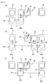
- the heat stages 21 and 22 are disposed such that the heat stage 22 on the right is set at the bump forming position located directly below the bonding head 40, as shown with a solid line.
- the heat stage 21 on the left is set at a position free of the bump forming position, namely, at a withdrawn position.
- the heat stage 21 on the left is set at the bump forming position located directly below the bonding head 40.
- the heat stage 22 on the right is set at a position free of the bump forming position, namely, at a withdrawn position, as shown with a chain line 22a.
- Each of the heat stages 21 and 22 contains a heater (not shown) that heats the wafer 2 placed thereon to a predetermined temperature before a bump forming process is performed on the wafer 2.
- each wafer 2 is conveyed by the stage shifting device 20 and a transferring device 30 that moves along the wafer magazines 12 and 14.
- the transferring device 30 transfers and extracts wafers 2 to and from the wafer magazines 12 and 14 using an arm 32 to be described hereinafter (see Figs. 6 to 9 ) that moves back and forth in a front-back direction (Y direction).
- the transferring device 30 When the shiftable table 23, that is, the heat stages 21 and 22, is positioned at the left side as indicated with a solid line, the transferring device 30 is set at a position indicated with a reference numeral 30b that faces the left heat stage 21 disposed at the withdrawn position so as to transfer or extract a wafer 2 to or from the heat stage 21.
- the transferring device 30 is set at a position indicated with a reference numeral 30c that faces the right heat stage 22 disposed at the withdrawn position so as to transfer or extract a wafer 2 to or from the heat stage 22.
- the transferring device 30 transfers wafers 2 from the wafer feeder magazine 12 to the stages 21 and 22 or transfers wafers 2 from the stages 21 and 22 to the wafer storage magazine 14 at different periods.
- the transferring device 30 at the position 30a facing the wafer feeder magazine 12 extracts a single wafer 2 from a plurality of wafers 2 packed horizontally in the wafer feeder magazine 12, as shown with an arrow L1. Subsequently, as shown with an arrow L2, the transferring device 30 transfers the wafer 2 to the position 30b facing the left heat stage 21. Then, the transferring device 30 places the wafer 2 on the left heat stage 21, as shown with an arrow L3, and positions the wafer 2 at a predetermined position. The wafer 2 placed on the left heat stage 21 is heated to a predetermined temperature (110° to 130°C).
- the heat stages 21 and 22 are shifted integrally to the right with the stage shifting device 20 so that the wafer 2 placed on the left heat stage 21 and preheated to the predetermined temperature (110° to 130°C) is disposed at the bump forming position located directly below the bonding head 40 of the bonding device.
- the bonding head 40 forms a bump on the wafer 2.
- the bonding head 40 uses an Au wire to form an Au ball on the wafer 2 heated to the predetermined temperature (110° to 130°C).
- the ball formed is bump-bonded (metallic-bonded) to an Al electrode of the wafer 2 by utilizing both the heat of the heat stage 21 at the predetermined temperature and ultrasonic vibration. This bump forming process is performed over the entire wafer 2.
- the transferring device 30 moves to the position 30c facing the right heat stage 22 and extracts a wafer 2 having a bump formed thereon from the right heat stage 22, as shown with an arrow R4. Subsequently, the wafer 2 having the bump is transferred to the position 30d facing the wafer storage magazine 14, as shown with an arrow R5, and is then stored in the wafer storage magazine 14, as shown with an arrow R6. Next, the transferring device 30 extracts a wafer 2 from the wafer feeder magazine 12 at the position 30a facing the wafer feeder magazine 12, as shown with an arrow R1. Then, the wafer 2 is transferred to the position 30c facing the right heat stage 22, as shown with an arrow R2. Subsequently, the wafer 2 is placed on the right heat stage 22, as shown with an arrow R3. The wafer 2 placed on the heat stage 22 is heated to a predetermined temperature.
- the heat stages 21 and 22 are shifted integrally to the left with the stage shifting device 20, as shown in Fig. 5(c) .
- the left heat stage 21 blows out air through air holes 24t of a stage body 24 to be described hereinafter (see Fig. 10 ) so as to allow the temperature of the wafer 2 placed thereon to decrease to a predetermined temperature (70° to 90°C).
- a predetermined value for example, 80°C
- clamp arms 26 open so that the wafer 2 can be transferred to the wafer storage magazine 14.
- the transferring device 30 moves to the position 30b facing the left heat stage 21 and extracts the wafer 2 with the bump formed thereon from the left heat stage 21, as shown with an arrow L4.
- the wafer 2 having the bump is then transferred to the position 30d facing the wafer storage magazine 14, as shown with an arrow L5.
- the wafer 2 is stored in the wafer storage magazine 14 in a horizontally packed manner.
- the bonding head 40 of the bonding device performs a bump forming process on the wafer 2 placed on the right heat stage 22.
- the heat stages 21 and 22 and the transferring device 30 will be described in further detail below with reference to Figs. 6 to 11 .
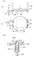
- each of the heat stages 21 and 22 has embedded therein a plurality of lifting pins 25 that are protrudable from an upper surface 24a of the stage body 24 holding a wafer 2.
- a plurality of lifting pins 25 that are protrudable from an upper surface 24a of the stage body 24 holding a wafer 2.
- Above the upper surface 24a of the stage body 24 is provided two positioning pins 28 protruding from the upper surface 24a and a pair of clamp arms 26.
- the arm 32 holding a wafer 2 advances from the main body 31 towards the corresponding one of the wafer magazines 12 and 14 (see Fig. 5 ) and heat stages 21 and 22, or recedes from the corresponding one.
- the arm 32 of the transferring device 30 advances towards the heat stage 21 or 22, as shown with an arrow 32a in Fig. 6 .
- the pair of clamp arms 26 is in an open state. In other words, the tip ends of the clamp arms 26 are withdrawn from a position on the upper surface 24a of the stage body 24 of the heat stage 21 or 22 where the wafer 2 is to be placed.
- the arm 32 of the transferring device 30 transfers the wafer 2 onto the stage body 24 (more specifically, above the lifting pins 25), the arm 32 descends as shown with an arrow 32b in Fig. 7 so as to be replaced by the lifting pins 25 for the supporting of the wafer 2. In other words, the wafer 2 is supported at the upper ends of the lifting pins 25.
- the arm 32 of the transferring device 30 remaining in the descent state recedes toward the main body 31 as shown with an arrow 32c in Fig. 8 .
- the lifting pins 25 supporting the wafer 2 descend as shown with an arrow 25a in Fig. 9 , so that the wafer 2 becomes placed on the upper surface 24a of the stage body 24.
- the clamp arms 26 rotate as shown with arrows 26a so as to become in a closed state. In this state, the tip ends of the clamp arms 26 are in contact with one side of the wafer 2 (left side in the drawings) so as to bias the wafer 2 toward the positioning pins 28. Consequently, the other side of the wafer 2 (right side in the drawings) is brought into contact with the positioning pins 28, whereby the wafer 2 is positioned. In this state, the wafer 2 is sandwiched between the clamp arms 26 and the positioning pins 28.
- the contact sections between the clamp arms 26 and the wafer 2 may be sections located at a side substantially opposite to the positioning pins 28, namely, to the left of the center assuming that the wafer 2 has a circular shape without an orientation flat portion, and where a bias force in the right direction (towards the positioning pins 28) is produced in the state where the clamp arms 26 are closed.
- a wafer 2 is positioned at a position where the center of the wafer 2 and the center of the stage body 24 substantially coincide with each other.
- the wafer 2 and the stage body 24 thermally expand outward from their centers. Therefore, if the positioning pins 28 have a fixed structure, a difference in the amount of displacement caused by different coefficients of thermal expansion between the stage body 24 and the wafer 2 cannot be absorbed, resulting in an excessive force to be imparted to sections of the wafer 2 that are in contact with the pins. This can lead to damaging of the wafer 2, such as formation of cracks.
- the positioning pins 28 are supported with leaf springs 27.
- the leaf springs 27 absorb the difference in the amount of displacement caused by different coefficients of thermal expansion between the stage body 24 and the wafer 2, thereby preventing an excessive force from being imparted to the wafer 2.
- the leaf springs 27 are disposed on a lower surface 24b of the stage body 24 of each heat stage 21 or 22. One end 27a of each leaf spring 27 is fixed to the lower surface 24b of the stage body 24 with a screw 29. A base end of each positioning pin 28 is fixed to the other end 27b of the corresponding leaf spring 27. The positioning pins 28 are loosely fitted in through holes 24s provided in the stage body 24 and protrude upward from the upper surface 24a of the stage body 24.
- the leaf springs 27 bend downward in the form of a substantially circular arc as shown with a chain line in the drawing, causing the positioning pins 28 to move rightward.
- the difference in the amount of displacement caused by different coefficients of thermal expansion between the stage body 24 and the wafer 2 is absorbed, thereby preventing the positioning pins 28 from imparting an excessive force to the wafer 2.
- the wafer 2 is biased by means of a spring force to be described hereinafter in detail, thereby preventing the clamp arms 26 from imparting an excessive force to the wafer 2.
- each clamp arm 26 has a contact surface 26s that is contactable with an outer periphery of the wafer 2.
- the contact surface 26s is inclined at a predetermined angle ⁇ (0° ⁇ ⁇ ⁇ 90°) with respect to the upper surface 24a of the stage body 24 and substantially faces the upper surface 24a of the stage body 24.
- each clamp arm 26 at least the contact surface 26s has electrical conductivity, and the contact surface 26s is grounded.
- the contact surfaces 26s of the clamp arms 26 come into contact with a ground electrode provided in an outer periphery area of the wafer 2. Consequently, the contact surfaces 26s remove an electric charge from the wafer 2, which is generated when the wafer 2 at room temperature having pyroelectric properties being placed on the heat stage 21 or 22 undergoes a temperature change. Due to being inclined, the contact surfaces 26s can properly come into contact with the ground electrode of the wafer 2, thereby ensuring the removal of electric charge from the wafer 2.
- the contact surfaces 26s move substantially in parallel towards the positioning pins 28 so as to come into contact with the outer periphery area of the wafer 2.
- the wafer 2 receives a force component parallel to the upper surface 24a of the stage body 24 and a downward force component orthogonal to the upper surface 24a of the stage body 24. Because the wafer 2 is pressed against the upper surface 24a of the stage body 24 by the downward force component, the wafer 2 is prevented from floating upward from the upper surface 24a of the stage body 24 even though the positioning pins 28 become tilted as shown with the chain line.
- the stage body 24 is provided with air holes 24t. With air drawn in through the air holes 24t, a lower surface 2b of the wafer 2 placed on the upper surface 24a can be held thereon by suction. By allowing air to flow into between the upper surface 24a and the lower surface 2b of the wafer 2 from the air holes 24t, the wafer 2 can be readily made to float and move above the upper surface 24a during the positioning of the wafer 2, or the wafer 2 can be cooled after the bump forming process.
- Fig. 11(a) is a plan view.
- Fig. 11(b) is a cross-sectional view taken along line B-B in Fig. 11(a) .
- the opening-closing mechanisms 120 and 140 for the pair of clamp arms 26 respectively have rotary shafts 124 and 144 that extend through and are rotatably supported by the stage body 24 of the heat stage 21 or 22.
- the base ends of the clamp arms 26 are fixed to upper ends of the respective rotary shafts 124 and 144.
- Lower ends of the rotary shafts 124 and 144 respectively have first ends of interlocking plates 126 and 146 fixed thereto.
- Second ends of the interlocking plates 126 and 146 overlap each other with a gap therebetween as shown in Fig. 11(b) , and respectively have through holes 127 and 147 at the overlapping sections.
- An engagement pin 132 projecting upward from a base member 130 is loosely fitted in these through holes 127 and 147.
- Extension springs have first ends secured to the lower surface of the stage body 24 and second ends secured to the interlocking plates 126 and 146. With a spring force of these extension springs, the interlocking plates 126 and 146 are biased in a direction indicated by arrows 128 and 148 in Fig. 11(a) .
- an actuator such as an extension cylinder (not shown)
- the base member 130 having the engagement pin 132 projecting therefrom rotates the interlocking plates 126 and 146 in a releasable manner in a direction indicated by an arrow 138 against the spring force of the extension springs acting in the direction of the arrows 128 and 148.
- the base member 130 moves in the direction of the arrow 138 so that the interlocking plates 126 and 146 overlap each other in a straight line, as shown with a chain line. Consequently, the clamp arms 26 become in an open state where the tip ends of the clamp arms 26 are distant from the wafer 2, as shown with a solid line.
- the temperature of each of the heat stages 21 and 22 is set at 70° to 90°C when a wafer 2 is not placed thereon, and at 100° to 130°C when a wafer 2 is placed thereon.
- the material used for the leaf springs 27 provided on each of the heat stages 21 and 22 is SUS304, and the material used for the positioning pins 28 and the clamp arms 26 is carbon steel, such as S50C, other alternative materials having electrical conductivity may be used.
- Positioning of a wafer 2 on the upper surface 24a of the stage body 24 of the heat stage 21 or 22 is implemented by closing the clamp arms 26 so that an orientation flat side comes into contact with the two positioning pins 28.
- the positioning pins 28 in contact with the orientation flat side of the wafer 2 are designed such that they are substantially prevented from being tilted or shifted, that is, the leaf springs 27 are substantially prevented from being bent, in response to the bias force of the clamp arms 26. Accordingly, this allows for proper positioning of the wafer 2.
- the leaf springs 27 may be locked by means of, for example, a cylinder to prevent the positioning pins 28 from being tilted or shifted vertically when the wafer 2 is being positioned by closing the clamp arms 26 and bringing the orientation flat side of the wafer 2 into contact with the positioning pins 28. In that case, the lock may be released when the temperature of the stage increases.
- each clamp arm 26 at least the contact surface 26s has electrical conductivity, and the contact surface 26s is grounded.
- the contact surfaces 26s of the clamp arms 26 come into contact with the ground electrode provided in the outer periphery area of the wafer 2. Consequently, the contact surfaces 26s can remove an electric charge from the wafer 2, which is generated when the wafer 2 at room temperature having pyroelectric properties being placed on the heat stage 21 or 22 undergoes an increase or decrease in temperature.
- a wafer 2 is configured such that a pyroelectric charge is unlikely to be generated, it may be preferable to shorten the time period required for lowering the temperature of the wafer 2 after the bump forming process. Specifically, this can be achieved by lifting the wafer 2 upward with the lifting pins 25 having electrical conductivity so that the lower surface of the wafer 2 is moved apart from the upper surface 24a of the stage body 24.
- a resiliently deformable member having a bimetallic structure is used.
- a resiliently deformable member having a bimetallic structure is formed of upper and lower layers of metallic materials having different coefficients of thermal expansion that are bonded to each other.
- the resiliently deformable member having the bimetallic structure bends voluntarily as the temperature of the wafer 2 increases, so as to cause the clamp arms 26 to move away from the wafer 2. This can prevent an excessive force from being imparted to the wafer 2.
- the stage configuration according to the first or second embodiment can be used in other apparatuses that are for processing wafers composed of a pyroelectric material and involve processes that induce a temperature change in the material.
- the stage configuration according to the first or second embodiment can be used in (a) an apparatus having a stage that measures the characteristics of a wafer during an aging process or after an aging process, (b) an apparatus having a stage that performs thermo-compression bonding on a chip at a wafer level under high temperature, and (c) an apparatus having a stage that performs ultrasonic bonding in combination with thermo-compression bonding on a chip at a wafer level under high temperature.
- the clamp arms 26 and the positioning pins 28 are given resilient characteristics so that a difference in the amount of displacement between the stage body 24 and the wafer 2 caused by thermal expansion can be absorbed. Accordingly, this can prevent damaging of the wafer 2, such as formation of cracks.
- the use of the clamp arms 26 having the inclined contact surfaces 26s significantly enhances the reliability for removing an electric charge from the wafer 2 in the case where the wafer 2 has pyroelectric properties.
Landscapes
- Engineering & Computer Science (AREA)
- Mechanical Engineering (AREA)
- Container, Conveyance, Adherence, Positioning, Of Wafer (AREA)
Abstract
Description
- The present invention relates to a positioning stage, a bump forming apparatus equipped with such a positioning stage, and a bump forming method performed using such a positioning stage.
- In manufacturing processes of electronic components, positioning stages for the positioning of wafers are generally used.
- For example, referring to
Fig. 1 , awafer receiver 66 provided on an end of a supportingarm 65 supports awafer 1. In a state wherepositioning rollers 67 are located outside the outer periphery of thewafer 1, astopper arm 72 is moved with respect to the supportingarm 65. Using a bias force of a spring, thepositioning rollers 67 andstopper rollers 74 sandwich thewafer 1 therebetween with an appropriate load (for example, see Patent Document 1). - In a case where a temperature change induces an electric charge, as in a piezoelectric substrate having pyroelectric properties, it is necessary to bring a charge-removing contact member into contact with a wafer placed on a positioning stage of a bump forming apparatus in order to remove the electric charge from the wafer. For example, referring to
Fig. 2 , a charge-removingmember 1416 is provided with a cone-shaped hole 14166, and aball 14115 provided at one end of a charge-removingcontact member 14121 has aground wire 14109 attached thereto. The other end of the charge-removingcontact member 14121 is provided with aball 14105 which is biased with aspring 14162. The charge-removingcontact member 14121 is brought into contact with a surface of a wafer so as to ground the electrically charged surface (for example, see Patent Document 2). - Patent Document 1: Japanese Unexamined Patent Application Publication No.
10-163214 Fig. 11 ) - Patent Document 2: Japanese Unexamined Patent Application Publication No.
2001-210664 - For example, when a wafer placed and positioned on a stage is heated in the course of a bump forming process, there are cases where the wafer gets damaged. This can occur when the heated wafer held in position undergoes thermal expansion, causing the internal stress generated within the wafer to exceed its strength.
- In the case where a temperature change induces an electric charge on a wafer, if the positioning and charge-removing steps for the wafer are to be performed separately, the overall process and the equipment therefor will be complicated. This makes it difficult to achieve higher production efficiency.
- In view of the circumstances described above, the present invention provides a positioning stage that prevents a wafer held in position from receiving an excessive force, and also provides a bump forming apparatus equipped with such a positioning stage and a bump forming method performed using such a positioning stage.
- In order to solve the aforementioned problems, the present invention provides a positioning stage as described below.
- A positioning stage includes a wafer-holding surface on which a wafer is placed; a positioning member that is disposed adjacent to the wafer placed on the wafer-holding surface and that extends substantially orthogonal to the wafer-holding surface; and a biasing member that is in contact with the wafer placed on the wafer-holding surface so as to resiliently bias the wafer towards the positioning member. The biasing member has a contact surface that substantially faces the wafer-holding surface at an angle, the contact surface being in contact with an outer periphery area of the wafer placed on the wafer-holding surface so as to bias the wafer slantwise towards the wafer-holding surface.
- Accordingly, the contact surface of the biasing member biases the outer periphery area of the wafer placed on the wafer-holding surface substantially towards the positioning member. Since the contact surface is inclined with respect to the wafer-holding surface, the wafer receives a force component parallel to the wafer-holding surface and a force component orthogonal to the wafer-holding surface and oriented towards the wafer-holding surface. With the latter force component, the wafer is pressed towards the wafer-holding surface. Thus, the wafer is prevented from floating upward from the wafer-holding surface while the wafer can be biased towards the positioning member. This prevents an excessive force from being imparted to the wafer, unlike a case where the biasing of a wafer towards a positioning member is implemented by only applying a force parallel to the wafer-holding surface onto the wafer.
- It is preferable that the biasing member has electrical conductivity in at least the contact surface.
- With this configuration, if the wafer is electrically charged, the contact surface of the biasing member having electrical conductivity may be brought into contact with the outer periphery area of the wafer so that the electric charge on the wafer can be removed through the contact surface of the biasing member.
- In order to solve the aforementioned problems, the present invention provides a positioning stage as described below.
- A positioning stage includes a wafer-holding surface on which a wafer is placed, and a positioning member that is disposed adjacent to the wafer placed on the wafer-holding surface and that extends substantially orthogonal to the wafer-holding surface. The positioning stage has a resiliently deformable member that brings the positioning member into contact with the wafer placed on the wafer-holding surface and holds the positioning member at a positioning position corresponding to where the wafer is positioned at a predetermined position. When a bias force exceeding a predetermined magnitude is imparted to the positioning member in a direction substantially opposite to the wafer placed on the wafer-holding surface, the resiliently deformable member becomes resiliently deformed so as to allow the positioning member to recede from the positioning position towards the direction substantially opposite to the wafer placed on the wafer-holding surface.
- In this configuration, since the positioning member in contact with the wafer can recede from the positioning position by resilient deformation of the resiliently deformable member, the wafer can be prevented from receiving a force exceeding a predetermined magnitude from the positioning member. Accordingly, this prevents an excessive force from being imparted to the positioned wafer.
- As a resiliently deformable member, a leaf spring or a bimetallic structure, for example, may be used. If a bimetallic structure is used, the resiliently deformable member becomes deformed voluntarily in response to a temperature change caused by heating of the positioning stage, thereby preliminarily preventing an occurrence of stress.
- In order to solve the aforementioned problems, the present invention provides a bump forming apparatus as described below.
- A bump forming apparatus includes two or more of the aforementioned positioning stages (which will simply be referred to as "stages" hereinafter); heating means for heating each of wafers placed on the wafer-holding surfaces of the stages; and stage shifting means for integrally shifting the stages between a bump forming position facing a bonding device and a withdrawn position withdrawn from the bump forming position. The stage shifting means sequentially shifts the stages to the bump forming position, and the bonding device forms a bump on a wafer placed on the wafer-holding surface of one of the stages positioned at the bump forming position while a wafer having a bump formed thereon placed on the wafer-holding surface of another stage positioned at the withdrawn position is removed from the wafer-holding surface of said another stage. A subsequent wafer to have a bump formed thereon is placed on the wafer-holding surface of said another stage and is heated by the heating means.
- In this configuration, the heating means may be provided inside of or outside of each of the stages.
- In addition to preventing an excessive force from being imparted to the positioned wafers, the above configuration can readily contribute to higher production efficiency since a wafer detachment process and a wafer heating process can be performed at one stage while a bump forming process is simultaneously performed at another stage.
- In order to solve the aforementioned problems, the present invention provides a bump forming method as described below.
- A bump forming method is performed using two or more of the aforementioned positioning stages (which will simply be referred to as "stages" hereinafter) to sequentially form bumps on wafers placed on the wafer-holding surfaces of the stages. The bump forming method includes a first step for disposing at least one of the stages at a bump forming position facing a bonding device while disposing at least another one of the stages at a withdrawn position withdrawn from the bump forming position; a second step for disposing the at least one of the stages at the withdrawn position while disposing the at least another one of the stages at the bump forming position; and repeating the first step and the second step while integrally shifting the stages. The first and second steps include allowing the bonding device to form a bump on a wafer placed on the wafer-holding surface of the stage disposed at the bonding position, and removing a wafer having a bump formed thereon from the wafer-holding surface of the stage disposed at the withdrawn position, and placing a subsequent wafer to have a bump formed thereon on the wafer-holding surface of the stage and heating the wafer.
- In addition to preventing an excessive force from being imparted to the positioned wafers, the above method can readily contribute to higher production efficiency since a wafer detachment process and a wafer heating process can be performed at one stage while a bump forming process is simultaneously performed at another stage. Advantages
- The positioning stage, the bump forming apparatus equipped with the positioning stage, and the bump forming method performed using the positioning stage according to the present invention prevent an excessive force from being imparted to a positioned wafer.
-
-
Fig. 1 illustrates a positioning mechanism for a wafer (related art). -
Fig. 2 illustrates a charge-removing mechanism (related art). -
Fig. 3 is a schematic plan view of a bump forming apparatus (embodiment). -
Fig. 4 illustrates a stage shifting device (embodiment). -
Fig. 5 illustrates an operation performed by the bump forming apparatus (embodiment). -
Fig. 6 illustrates a wafer transferring process (embodiment). -
Fig. 7 also illustrates the wafer transferring process (embodiment). -
Fig. 8 also illustrates the wafer transferring process (embodiment). -
Fig. 9 also illustrates the wafer transferring process (embodiment). -
Fig. 10 is a cross-sectional view of a stage (embodiment). -
Fig. 11 includes a plan view (a) and a cross-sectional view (b) of the stage (embodiment). -
- 2
- wafer
- 10
- bump forming apparatus
- 20
- stage shifting device (stage shifting means)
- 21, 22
- heat stage (positioning stage)
- 24
- stage body
- 24a
- upper surface (wafer-holding surface)
- 26
- clamp arm (biasing member)
- 26s
- contact surface
- 27
- leaf spring (resiliently deformable member)
- 28
- positioning pin (positioning member)
- Embodiments of the present invention will now be described with reference to
Figs. 3 to 11 . - As shown in a plan view of
Fig. 3 , abump forming apparatus 10 forms bumps alternately onwafers 2 placed on twoheat stages - Each
wafer 2 is composed of a piezoelectric material having pyroelectric properties, such as lithium tantalate (LiTaO3) or lithium niobate (LiNbO3), used for forming, for example, a surface-acoustic-wave (SAW) filter. Thewafer 2 has a ground electrode on an outer periphery area thereof. - In the apparatus shown in
Fig. 3 , the twoheat stages stage shifting device 20 so that the heat stages 21 and 22 are alternately disposed at a bump forming position located directly below abonding head 40 of a bonding device. When each of the heat stages 21 and 22 is disposed at the bump forming position, thebonding head 40 forms a bump on thewafer 2 placed on the heat stage. Awafer feeder magazine 12 and awafer storage magazine 14 are disposed at opposite sides of thestage shifting device 20. - Referring to
Fig. 4 , thestage shifting device 20 has a single shiftable table 23 that is shiftable in the left-right direction (X direction). The shiftable table 23 has the heat stages 21 and 22 fixed thereon and is driven by an actuator, such as a motor (not shown), so as to be shifted between left and right positions. The heat stages 21 and 22 move integrally with the shifting of the shiftable table 23. - When the shiftable table 23 is positioned at the left side in the drawing, the heat stages 21 and 22 are disposed such that the
heat stage 22 on the right is set at the bump forming position located directly below thebonding head 40, as shown with a solid line. On the other hand, theheat stage 21 on the left is set at a position free of the bump forming position, namely, at a withdrawn position. - When the shiftable table 23 is positioned at the right side in the drawing, the
heat stage 21 on the left is set at the bump forming position located directly below thebonding head 40. On the other hand, theheat stage 22 on the right is set at a position free of the bump forming position, namely, at a withdrawn position, as shown with achain line 22a. - Each of the heat stages 21 and 22 contains a heater (not shown) that heats the
wafer 2 placed thereon to a predetermined temperature before a bump forming process is performed on thewafer 2. - Referring to
Fig. 3 , eachwafer 2 is conveyed by thestage shifting device 20 and a transferringdevice 30 that moves along thewafer magazines - At a position facing the
wafer magazine 12 indicated with areference numeral 30a and a position facing thewafer magazine 14 indicated with areference numeral 30d, the transferringdevice 30 transfers andextracts wafers 2 to and from thewafer magazines arm 32 to be described hereinafter (seeFigs. 6 to 9 ) that moves back and forth in a front-back direction (Y direction). - When the shiftable table 23, that is, the heat stages 21 and 22, is positioned at the left side as indicated with a solid line, the transferring
device 30 is set at a position indicated with areference numeral 30b that faces theleft heat stage 21 disposed at the withdrawn position so as to transfer or extract awafer 2 to or from theheat stage 21. When the shiftable table 23, that is, the heat stages 21 and 22, is positioned at the right side, the transferringdevice 30 is set at a position indicated with areference numeral 30c that faces theright heat stage 22 disposed at the withdrawn position so as to transfer or extract awafer 2 to or from theheat stage 22. - Based on the above operation, the transferring
device 30transfers wafers 2 from thewafer feeder magazine 12 to thestages transfers wafers 2 from thestages wafer storage magazine 14 at different periods. - An overall operation for forming bumps on
wafers 2 using thebump forming apparatus 10 will now be described with reference toFig. 5 . - Referring to
Fig. 5(a) , when the heat stages 21 and 22 are shifted to the left with thestage shifting device 20, the transferringdevice 30 at theposition 30a facing thewafer feeder magazine 12 extracts asingle wafer 2 from a plurality ofwafers 2 packed horizontally in thewafer feeder magazine 12, as shown with an arrow L1. Subsequently, as shown with an arrow L2, the transferringdevice 30 transfers thewafer 2 to theposition 30b facing theleft heat stage 21. Then, the transferringdevice 30 places thewafer 2 on theleft heat stage 21, as shown with an arrow L3, and positions thewafer 2 at a predetermined position. Thewafer 2 placed on theleft heat stage 21 is heated to a predetermined temperature (110° to 130°C). - Subsequently, referring to
Fig. 5(b) , the heat stages 21 and 22 are shifted integrally to the right with thestage shifting device 20 so that thewafer 2 placed on theleft heat stage 21 and preheated to the predetermined temperature (110° to 130°C) is disposed at the bump forming position located directly below thebonding head 40 of the bonding device. At the bump forming position, thebonding head 40 forms a bump on thewafer 2. - Specifically, based on a correction between graphic coordinates on the
wafer 2 and coordinates on an X-Y table of thebonding head 40 performed using an image recognition device and a reference mark provided on thewafer 2, thebonding head 40 uses an Au wire to form an Au ball on thewafer 2 heated to the predetermined temperature (110° to 130°C). The ball formed is bump-bonded (metallic-bonded) to an Al electrode of thewafer 2 by utilizing both the heat of theheat stage 21 at the predetermined temperature and ultrasonic vibration. This bump forming process is performed over theentire wafer 2. - In the meantime, the transferring
device 30 moves to theposition 30c facing theright heat stage 22 and extracts awafer 2 having a bump formed thereon from theright heat stage 22, as shown with an arrow R4. Subsequently, thewafer 2 having the bump is transferred to theposition 30d facing thewafer storage magazine 14, as shown with an arrow R5, and is then stored in thewafer storage magazine 14, as shown with an arrow R6. Next, the transferringdevice 30 extracts awafer 2 from thewafer feeder magazine 12 at theposition 30a facing thewafer feeder magazine 12, as shown with an arrow R1. Then, thewafer 2 is transferred to theposition 30c facing theright heat stage 22, as shown with an arrow R2. Subsequently, thewafer 2 is placed on theright heat stage 22, as shown with an arrow R3. Thewafer 2 placed on theheat stage 22 is heated to a predetermined temperature. - When the bump forming process performed on the
entire wafer 2 placed on theleft heat stage 21 is completed, the heat stages 21 and 22 are shifted integrally to the left with thestage shifting device 20, as shown inFig. 5(c) . Theleft heat stage 21 blows out air throughair holes 24t of astage body 24 to be described hereinafter (seeFig. 10 ) so as to allow the temperature of thewafer 2 placed thereon to decrease to a predetermined temperature (70° to 90°C). When the temperature of thewafer 2 reaches a predetermined value (for example, 80°C), clamp arms 26 (seeFigs. 6 to 10 ) open so that thewafer 2 can be transferred to thewafer storage magazine 14. In other words, the transferringdevice 30 moves to theposition 30b facing theleft heat stage 21 and extracts thewafer 2 with the bump formed thereon from theleft heat stage 21, as shown with an arrow L4. Thewafer 2 having the bump is then transferred to theposition 30d facing thewafer storage magazine 14, as shown with an arrow L5. Subsequently, as shown with an arrow L6, thewafer 2 is stored in thewafer storage magazine 14 in a horizontally packed manner. - In the meantime, the
bonding head 40 of the bonding device performs a bump forming process on thewafer 2 placed on theright heat stage 22. - By alternately using the heat stages 21 and 22 in synchronization with the shifting of the heat stages 21 and 22, the same processes are performed at different periods so that the bumps can be formed efficiently.
- The heat stages 21 and 22 and the transferring
device 30 will be described in further detail below with reference toFigs. 6 to 11 . - Referring to
Figs. 6 to 9 , each of the heat stages 21 and 22 has embedded therein a plurality of liftingpins 25 that are protrudable from anupper surface 24a of thestage body 24 holding awafer 2. Above theupper surface 24a of thestage body 24 is provided twopositioning pins 28 protruding from theupper surface 24a and a pair ofclamp arms 26. - When a
main body 31 of the transferringdevice 30 is located at any of thepositions 30a to 30d (seeFig. 5 ) facing thewafer magazines 12 and 14 (seeFig. 5 ) and heat stages 21 and 22, thearm 32 holding awafer 2 advances from themain body 31 towards the corresponding one of thewafer magazines 12 and 14 (seeFig. 5 ) and heat stages 21 and 22, or recedes from the corresponding one. - An operation performed when the transferring
device 30 places awafer 2 on theupper surface 24a of thestage body 24 of theheat stage Figs. 6 to 9 . - While holding a
wafer 2, thearm 32 of the transferringdevice 30 advances towards theheat stage arrow 32a inFig. 6 . At this time, the pair ofclamp arms 26 is in an open state. In other words, the tip ends of theclamp arms 26 are withdrawn from a position on theupper surface 24a of thestage body 24 of theheat stage wafer 2 is to be placed. - When the
arm 32 of the transferringdevice 30 transfers thewafer 2 onto the stage body 24 (more specifically, above the lifting pins 25), thearm 32 descends as shown with anarrow 32b inFig. 7 so as to be replaced by the lifting pins 25 for the supporting of thewafer 2. In other words, thewafer 2 is supported at the upper ends of the lifting pins 25. - Subsequently, the
arm 32 of the transferringdevice 30 remaining in the descent state recedes toward themain body 31 as shown with anarrow 32c inFig. 8 . - Then, the lifting pins 25 supporting the
wafer 2 descend as shown with anarrow 25a inFig. 9 , so that thewafer 2 becomes placed on theupper surface 24a of thestage body 24. Next, theclamp arms 26 rotate as shown witharrows 26a so as to become in a closed state. In this state, the tip ends of theclamp arms 26 are in contact with one side of the wafer 2 (left side in the drawings) so as to bias thewafer 2 toward the positioning pins 28. Consequently, the other side of the wafer 2 (right side in the drawings) is brought into contact with the positioning pins 28, whereby thewafer 2 is positioned. In this state, thewafer 2 is sandwiched between theclamp arms 26 and the positioning pins 28. - The contact sections between the
clamp arms 26 and thewafer 2 may be sections located at a side substantially opposite to the positioning pins 28, namely, to the left of the center assuming that thewafer 2 has a circular shape without an orientation flat portion, and where a bias force in the right direction (towards the positioning pins 28) is produced in the state where theclamp arms 26 are closed. - The structure of the heat stages 21 and 22 will now be described with reference to a cross-sectional view in
Fig. 10 . - A
wafer 2 is positioned at a position where the center of thewafer 2 and the center of thestage body 24 substantially coincide with each other. Thewafer 2 and thestage body 24 thermally expand outward from their centers. Therefore, if the positioning pins 28 have a fixed structure, a difference in the amount of displacement caused by different coefficients of thermal expansion between thestage body 24 and thewafer 2 cannot be absorbed, resulting in an excessive force to be imparted to sections of thewafer 2 that are in contact with the pins. This can lead to damaging of thewafer 2, such as formation of cracks. - To prevent this, the positioning pins 28 are supported with
leaf springs 27. By resilient deformation, theleaf springs 27 absorb the difference in the amount of displacement caused by different coefficients of thermal expansion between thestage body 24 and thewafer 2, thereby preventing an excessive force from being imparted to thewafer 2. - The leaf springs 27 are disposed on a
lower surface 24b of thestage body 24 of eachheat stage end 27a of eachleaf spring 27 is fixed to thelower surface 24b of thestage body 24 with ascrew 29. A base end of eachpositioning pin 28 is fixed to theother end 27b of the correspondingleaf spring 27. The positioning pins 28 are loosely fitted in throughholes 24s provided in thestage body 24 and protrude upward from theupper surface 24a of thestage body 24. - When a force exceeding a predetermined magnitude is imparted rightward to the tip ends of the positioning pins 28, the
leaf springs 27 bend downward in the form of a substantially circular arc as shown with a chain line in the drawing, causing the positioning pins 28 to move rightward. Thus, the difference in the amount of displacement caused by different coefficients of thermal expansion between thestage body 24 and thewafer 2 is absorbed, thereby preventing the positioning pins 28 from imparting an excessive force to thewafer 2. - On the other hand, with regard to the
clamp arms 26 biasing thewafer 2, thewafer 2 is biased by means of a spring force to be described hereinafter in detail, thereby preventing theclamp arms 26 from imparting an excessive force to thewafer 2. - The tip end of each
clamp arm 26 has acontact surface 26s that is contactable with an outer periphery of thewafer 2. Thecontact surface 26s is inclined at a predetermined angle θ (0° < θ < 90°) with respect to theupper surface 24a of thestage body 24 and substantially faces theupper surface 24a of thestage body 24. - In each
clamp arm 26, at least thecontact surface 26s has electrical conductivity, and thecontact surface 26s is grounded. When theclamp arms 26 close, the contact surfaces 26s of theclamp arms 26 come into contact with a ground electrode provided in an outer periphery area of thewafer 2. Consequently, the contact surfaces 26s remove an electric charge from thewafer 2, which is generated when thewafer 2 at room temperature having pyroelectric properties being placed on theheat stage wafer 2, thereby ensuring the removal of electric charge from thewafer 2. - When the
clamp arms 26 are being closed, the contact surfaces 26s move substantially in parallel towards the positioning pins 28 so as to come into contact with the outer periphery area of thewafer 2. In this case, thewafer 2 receives a force component parallel to theupper surface 24a of thestage body 24 and a downward force component orthogonal to theupper surface 24a of thestage body 24. Because thewafer 2 is pressed against theupper surface 24a of thestage body 24 by the downward force component, thewafer 2 is prevented from floating upward from theupper surface 24a of thestage body 24 even though the positioning pins 28 become tilted as shown with the chain line. - The
stage body 24 is provided withair holes 24t. With air drawn in through theair holes 24t, alower surface 2b of thewafer 2 placed on theupper surface 24a can be held thereon by suction. By allowing air to flow into between theupper surface 24a and thelower surface 2b of thewafer 2 from theair holes 24t, thewafer 2 can be readily made to float and move above theupper surface 24a during the positioning of thewafer 2, or thewafer 2 can be cooled after the bump forming process. - Next, opening-
closing mechanisms clamp arms 26 will be described with reference toFig. 11. Fig. 11(a) is a plan view.Fig. 11(b) is a cross-sectional view taken along line B-B inFig. 11(a) . - The opening-
closing mechanisms clamp arms 26 respectively haverotary shafts stage body 24 of theheat stage clamp arms 26 are fixed to upper ends of therespective rotary shafts rotary shafts plates plates Fig. 11(b) , and respectively have throughholes engagement pin 132 projecting upward from abase member 130 is loosely fitted in these throughholes stage body 24 and second ends secured to the interlockingplates plates arrows Fig. 11(a) . By being driven by an actuator, such as an extension cylinder (not shown), thebase member 130 having theengagement pin 132 projecting therefrom rotates the interlockingplates arrow 138 against the spring force of the extension springs acting in the direction of thearrows - When the
wafer 2 is to be detached from theupper surface 24a of thestage body 24 of theheat stage base member 130 moves in the direction of thearrow 138 so that the interlockingplates clamp arms 26 become in an open state where the tip ends of theclamp arms 26 are distant from thewafer 2, as shown with a solid line. - When the
wafer 2 is to be held on theupper surface 24a of thestage body 24 of theheat stage base member 130 is cancelled, so that the spring force of the extension springs acting in the direction of thearrows plates plates clamp arms 26, whereby theclamp arms 26 become in a closed state where the tip ends of theclamp arms 26 are in contact with the outer periphery of thewafer 2. - The temperature of each of the heat stages 21 and 22 is set at 70° to 90°C when a
wafer 2 is not placed thereon, and at 100° to 130°C when awafer 2 is placed thereon. - Although the material used for the leaf springs 27 provided on each of the heat stages 21 and 22 is SUS304, and the material used for the positioning pins 28 and the
clamp arms 26 is carbon steel, such as S50C, other alternative materials having electrical conductivity may be used. - Positioning of a
wafer 2 on theupper surface 24a of thestage body 24 of theheat stage clamp arms 26 so that an orientation flat side comes into contact with the two positioning pins 28. In this case, the positioning pins 28 in contact with the orientation flat side of thewafer 2 are designed such that they are substantially prevented from being tilted or shifted, that is, theleaf springs 27 are substantially prevented from being bent, in response to the bias force of theclamp arms 26. Accordingly, this allows for proper positioning of thewafer 2. - Instead of such a design, the
leaf springs 27 may be locked by means of, for example, a cylinder to prevent the positioning pins 28 from being tilted or shifted vertically when thewafer 2 is being positioned by closing theclamp arms 26 and bringing the orientation flat side of thewafer 2 into contact with the positioning pins 28. In that case, the lock may be released when the temperature of the stage increases. - In each
clamp arm 26, at least thecontact surface 26s has electrical conductivity, and thecontact surface 26s is grounded. When theclamp arms 26 close while awafer 2 is placed on theheat stage clamp arms 26 come into contact with the ground electrode provided in the outer periphery area of thewafer 2. Consequently, the contact surfaces 26s can remove an electric charge from thewafer 2, which is generated when thewafer 2 at room temperature having pyroelectric properties being placed on theheat stage - In a case where a
wafer 2 is configured such that a pyroelectric charge is unlikely to be generated, it may be preferable to shorten the time period required for lowering the temperature of thewafer 2 after the bump forming process. Specifically, this can be achieved by lifting thewafer 2 upward with the lifting pins 25 having electrical conductivity so that the lower surface of thewafer 2 is moved apart from theupper surface 24a of thestage body 24. - In place of the
leaf springs 27, a resiliently deformable member having a bimetallic structure is used. In detail, a resiliently deformable member having a bimetallic structure is formed of upper and lower layers of metallic materials having different coefficients of thermal expansion that are bonded to each other. - Thus, the resiliently deformable member having the bimetallic structure bends voluntarily as the temperature of the
wafer 2 increases, so as to cause theclamp arms 26 to move away from thewafer 2. This can prevent an excessive force from being imparted to thewafer 2. - In addition to bump forming apparatuses, the stage configuration according to the first or second embodiment can be used in other apparatuses that are for processing wafers composed of a pyroelectric material and involve processes that induce a temperature change in the material.
- For example, the stage configuration according to the first or second embodiment can be used in (a) an apparatus having a stage that measures the characteristics of a wafer during an aging process or after an aging process, (b) an apparatus having a stage that performs thermo-compression bonding on a chip at a wafer level under high temperature, and (c) an apparatus having a stage that performs ultrasonic bonding in combination with thermo-compression bonding on a chip at a wafer level under high temperature.
- As described above, the
clamp arms 26 and the positioning pins 28 are given resilient characteristics so that a difference in the amount of displacement between thestage body 24 and thewafer 2 caused by thermal expansion can be absorbed. Accordingly, this can prevent damaging of thewafer 2, such as formation of cracks. In addition, the use of theclamp arms 26 having the inclined contact surfaces 26s significantly enhances the reliability for removing an electric charge from thewafer 2 in the case where thewafer 2 has pyroelectric properties. - The present invention is not limited to the above embodiments, and various modifications are permissible.
Claims (3)
- A positioning stage comprising:a wafer-holding surface on which a wafer is placed; anda positioning member that is disposed adjacent to the wafer placed on the wafer-holding surface and that extends substantially orthogonal to the wafer-holding surface,wherein the positioning stage includes a resiliently deformable member that brings the positioning member into contact with the wafer placed on the wafer-holding surface and holds the positioning member at a positioning position corresponding to where the wafer is positioned at a predetermined position, and
wherein when a bias force exceeding a predetermined magnitude is imparted to the positioning member in a direction substantially opposite to the wafer placed on the wafer-holding surface, the resiliently deformable member becomes resiliently deformed so as to allow the positioning member to recede from the positioning position towards the direction substantially opposite to the wafer placed on the wafer-holding surface. - A bump forming apparatus comprising:two or more of the positioning stages according to claim 3;heating means for heating each of wafers placed on the wafer-holding surfaces of the stages; andstage shifting means for shifting each stage between a bump forming position facing a bonding device and a withdrawn position withdrawn from the bump forming position,wherein the stage shifting means sequentially shifts the stages to the bump forming position, wherein the bonding device forms a bump on a wafer placed on the wafer-holding surface of one of the stages positioned at the bump forming position while a wafer having a bump formed thereon placed on the wafer-holding surface of another stage positioned at the withdrawn position is removed from the wafer-holding surface of said another stage, and wherein a subsequent wafer to have a bump formed thereon is placed on the wafer-holding surface of said another stage and is heated by the heating means.
- A bump forming method performed using two or more of the positioning stages according to claim 3 to sequentially form bumps on wafers placed on the wafer-holding surfaces of the stages, the method comprising:a first step for disposing at least one of the stages at a bump forming position facing a bonding device while disposing at least another one of the stages at a withdrawn position withdrawn from the bump forming position;a second step for disposing said at least one of the stages at the withdrawn position while disposing said at least another one of the stages at the bump forming position; andrepeating the first step and the second step while shifting the stages,wherein the first and second steps include allowing the bonding device to form a bump on a wafer placed on the wafer-holding surface of the stage disposed at the bonding position, and
removing a wafer having a bump formed thereon from the wafer-holding surface of the stage disposed at the withdrawn position, and placing a subsequent wafer to have a bump formed thereon on the wafer-holding surface of the stage and heating the wafer.
Applications Claiming Priority (2)
| Application Number | Priority Date | Filing Date | Title |
|---|---|---|---|
| JP2005145259 | 2005-05-18 | ||
| EP06746350.5A EP1890325B1 (en) | 2005-05-18 | 2006-05-12 | Aligning stage, bump forming apparatus and bump forming method using such aligning stage |
Related Parent Applications (2)
| Application Number | Title | Priority Date | Filing Date |
|---|---|---|---|
| EP06746350.5 Division | 2006-05-12 | ||
| EP06746350.5A Division EP1890325B1 (en) | 2005-05-18 | 2006-05-12 | Aligning stage, bump forming apparatus and bump forming method using such aligning stage |
Publications (2)
| Publication Number | Publication Date |
|---|---|
| EP2197027A2 true EP2197027A2 (en) | 2010-06-16 |
| EP2197027A3 EP2197027A3 (en) | 2017-04-26 |
Family
ID=37431167
Family Applications (2)
| Application Number | Title | Priority Date | Filing Date |
|---|---|---|---|
| EP06746350.5A Active EP1890325B1 (en) | 2005-05-18 | 2006-05-12 | Aligning stage, bump forming apparatus and bump forming method using such aligning stage |
| EP10003566.6A Withdrawn EP2197027A3 (en) | 2005-05-18 | 2006-05-12 | Positioning stage, bump forming apparatus equipped with the positioning stage, and bump forming method performed using the positioning stage |
Family Applications Before (1)
| Application Number | Title | Priority Date | Filing Date |
|---|---|---|---|
| EP06746350.5A Active EP1890325B1 (en) | 2005-05-18 | 2006-05-12 | Aligning stage, bump forming apparatus and bump forming method using such aligning stage |
Country Status (5)
| Country | Link |
|---|---|
| US (1) | US7508495B2 (en) |
| EP (2) | EP1890325B1 (en) |
| JP (2) | JP4636288B2 (en) |
| CN (1) | CN101176201B (en) |
| WO (1) | WO2006123592A1 (en) |
Families Citing this family (3)
| Publication number | Priority date | Publication date | Assignee | Title |
|---|---|---|---|---|
| US20120083129A1 (en) | 2010-10-05 | 2012-04-05 | Skyworks Solutions, Inc. | Apparatus and methods for focusing plasma |
| US9478428B2 (en) | 2010-10-05 | 2016-10-25 | Skyworks Solutions, Inc. | Apparatus and methods for shielding a plasma etcher electrode |
| CN113013082B (en) * | 2021-03-01 | 2022-09-13 | 深圳市容微精密电子有限公司 | Fixture mechanism for wafer detection |
Citations (2)
| Publication number | Priority date | Publication date | Assignee | Title |
|---|---|---|---|---|
| JPH10163214A (en) | 1996-12-03 | 1998-06-19 | Matsushita Electric Ind Co Ltd | Bump bonder and bump forming method |
| JP2001210664A (en) | 1999-07-02 | 2001-08-03 | Matsushita Electric Ind Co Ltd | Bump forming apparatus for charge generation semiconductor substrate, charge elimination method for charge generation semiconductor substrate, charge elimination apparatus for charge generation semiconductor substrate, and charge generation semiconductor substrate |
Family Cites Families (16)
| Publication number | Priority date | Publication date | Assignee | Title |
|---|---|---|---|---|
| JPS60167245A (en) * | 1984-02-10 | 1985-08-30 | Hitachi Ltd | Sample holding device |
| JPH03204937A (en) * | 1989-12-30 | 1991-09-06 | Casio Comput Co Ltd | Method of plating wafers |
| JPH04110466A (en) * | 1990-08-31 | 1992-04-10 | Oki Electric Ind Co Ltd | Wafer holder |
| JP3175058B2 (en) * | 1991-10-16 | 2001-06-11 | 株式会社ニコン | Substrate positioning device and substrate positioning method |
| US6172738B1 (en) * | 1996-09-24 | 2001-01-09 | Canon Kabushiki Kaisha | Scanning exposure apparatus and device manufacturing method using the same |
| JP3655787B2 (en) * | 1999-07-02 | 2005-06-02 | 松下電器産業株式会社 | Bump forming apparatus for charge generation substrate and charge removal method for charge generation substrate |
| JP2001118871A (en) * | 1999-10-15 | 2001-04-27 | Matsushita Electric Ind Co Ltd | Bump forming apparatus and bump forming method |
| TW452917B (en) * | 1999-10-29 | 2001-09-01 | Winbond Electronics Corp | Holder |
| JP4364393B2 (en) * | 2000-03-23 | 2009-11-18 | パナソニック株式会社 | Handling method of bonding object and bump bonding apparatus using the same |
| US6692219B2 (en) * | 2000-11-29 | 2004-02-17 | Tokyo Electron Limited | Reduced edge contact wafer handling system and method of retrofitting and using same |
| JP2002203995A (en) * | 2000-12-27 | 2002-07-19 | Toshiba Corp | Substrate heating method, substrate cooling method, and their devices |
| US6614190B2 (en) * | 2001-01-31 | 2003-09-02 | Hitachi, Ltd. | Ion implanter |
| US6949177B2 (en) | 2001-08-16 | 2005-09-27 | Oriol Inc. | System and method for processing semiconductor wafers using different wafer processes |
| JP4832682B2 (en) * | 2001-09-18 | 2011-12-07 | 東京エレクトロン株式会社 | Automated guided vehicle |
| US6806943B2 (en) * | 2002-08-09 | 2004-10-19 | International Business Machines Corporation | Mask clamping device |
| DE602004020634D1 (en) * | 2003-08-07 | 2009-05-28 | Nippon Kogaku Kk | EXPOSURE METHOD |
-
2006
- 2006-05-12 EP EP06746350.5A patent/EP1890325B1/en active Active
- 2006-05-12 JP JP2007516271A patent/JP4636288B2/en active Active
- 2006-05-12 CN CN2006800168627A patent/CN101176201B/en active Active
- 2006-05-12 WO PCT/JP2006/309603 patent/WO2006123592A1/en not_active Ceased
- 2006-05-12 EP EP10003566.6A patent/EP2197027A3/en not_active Withdrawn
-
2007
- 2007-11-19 US US11/942,320 patent/US7508495B2/en active Active
-
2010
- 2010-09-13 JP JP2010204940A patent/JP5381940B2/en active Active
Patent Citations (2)
| Publication number | Priority date | Publication date | Assignee | Title |
|---|---|---|---|---|
| JPH10163214A (en) | 1996-12-03 | 1998-06-19 | Matsushita Electric Ind Co Ltd | Bump bonder and bump forming method |
| JP2001210664A (en) | 1999-07-02 | 2001-08-03 | Matsushita Electric Ind Co Ltd | Bump forming apparatus for charge generation semiconductor substrate, charge elimination method for charge generation semiconductor substrate, charge elimination apparatus for charge generation semiconductor substrate, and charge generation semiconductor substrate |
Also Published As
| Publication number | Publication date |
|---|---|
| CN101176201A (en) | 2008-05-07 |
| CN101176201B (en) | 2011-04-27 |
| US20080068581A1 (en) | 2008-03-20 |
| US7508495B2 (en) | 2009-03-24 |
| JP2010278478A (en) | 2010-12-09 |
| EP1890325B1 (en) | 2014-01-01 |
| EP1890325A4 (en) | 2008-09-17 |
| EP2197027A3 (en) | 2017-04-26 |
| WO2006123592A1 (en) | 2006-11-23 |
| EP1890325A1 (en) | 2008-02-20 |
| JP5381940B2 (en) | 2014-01-08 |
| JPWO2006123592A1 (en) | 2008-12-25 |
| JP4636288B2 (en) | 2011-02-23 |
Similar Documents
| Publication | Publication Date | Title |
|---|---|---|
| US8910375B2 (en) | Mounting apparatus | |
| KR100446262B1 (en) | Electric charge generating semiconductor substrate bump forming device, method of removing electric charge from electric charge generating semiconductor substrate, device for removing electric charge from electric charge generating semiconductor substrate, and electric charge generating semiconductor substrate | |
| US20080179378A1 (en) | Method of forming bumps on a wafer utilizing a post-heating operation, and an apparatus therefore | |
| US7508495B2 (en) | Positioning stage, bump forming apparatus equipped with the positioning stage, and bump forming method performed using the positioning stage | |
| KR20230071749A (en) | An electrode assembly, an apparatus for manufacturing the same, and a manufacturing method thereof | |
| JPH08130230A (en) | Flip chip mounting equipment | |
| US8137050B2 (en) | Pickup device and pickup method | |
| JP5257149B2 (en) | Solder removing apparatus and solder removing method | |
| KR930007541B1 (en) | Gripping devices for articles such as integrated circuit leadframes | |
| JP3667241B2 (en) | Bonding method and apparatus | |
| KR102185034B1 (en) | Module for aligning bonding tool and die bonding apparatus having the same | |
| JP4570210B2 (en) | Bump forming device for charge generation substrate | |
| JP5052085B2 (en) | Pickup device | |
| JP3655787B2 (en) | Bump forming apparatus for charge generation substrate and charge removal method for charge generation substrate | |
| JP3571398B2 (en) | Bump forming method and apparatus | |
| JP3858719B2 (en) | Reinforcing materials for semiconductor devices | |
| WO2023228293A1 (en) | Bonding apparatus and bonding method | |
| JP2005159373A (en) | Bump forming apparatus for charge generating semiconductor substrate and charge eliminating method for charge generating semiconductor substrate | |
| KR20040023538A (en) | Bump forming method and apparatus for heating and compressing bump materials inserted in positioning holes | |
| KR20200135268A (en) | Module for aligning bonding tool and die bonding apparatus having the same | |
| JP2000124340A (en) | Cap bonding jig |
Legal Events
| Date | Code | Title | Description |
|---|---|---|---|
| PUAI | Public reference made under article 153(3) epc to a published international application that has entered the european phase |
Free format text: ORIGINAL CODE: 0009012 |
|
| 17P | Request for examination filed |
Effective date: 20100331 |
|
| AC | Divisional application: reference to earlier application |
Ref document number: 1890325 Country of ref document: EP Kind code of ref document: P |
|
| AK | Designated contracting states |
Kind code of ref document: A2 Designated state(s): AT BE BG CH CY CZ DE DK EE ES FI FR GB GR HU IE IS IT LI LT LU LV MC NL PL PT RO SE SI SK TR |
|
| PUAL | Search report despatched |
Free format text: ORIGINAL CODE: 0009013 |
|
| AK | Designated contracting states |
Kind code of ref document: A3 Designated state(s): AT BE BG CH CY CZ DE DK EE ES FI FR GB GR HU IE IS IT LI LT LU LV MC NL PL PT RO SE SI SK TR |
|
| RIC1 | Information provided on ipc code assigned before grant |
Ipc: B23K 3/06 20060101ALI20170317BHEP Ipc: B23K 101/40 20060101ALN20170317BHEP Ipc: H01L 21/60 20060101ALI20170317BHEP Ipc: H01L 21/687 20060101ALI20170317BHEP Ipc: H01L 23/00 20060101ALI20170317BHEP Ipc: H01L 21/68 20060101AFI20170317BHEP |
|
| STAA | Information on the status of an ep patent application or granted ep patent |
Free format text: STATUS: THE APPLICATION HAS BEEN WITHDRAWN |
|
| 18W | Application withdrawn |
Effective date: 20180702 |