EP2196948B1 - Mobile object inductively coupled to a fixed station and including gain control methods - Google Patents
Mobile object inductively coupled to a fixed station and including gain control methods Download PDFInfo
- Publication number
- EP2196948B1 EP2196948B1 EP09178424A EP09178424A EP2196948B1 EP 2196948 B1 EP2196948 B1 EP 2196948B1 EP 09178424 A EP09178424 A EP 09178424A EP 09178424 A EP09178424 A EP 09178424A EP 2196948 B1 EP2196948 B1 EP 2196948B1
- Authority
- EP
- European Patent Office
- Prior art keywords
- voltage
- rectifier
- output
- difference
- input
- Prior art date
- Legal status (The legal status is an assumption and is not a legal conclusion. Google has not performed a legal analysis and makes no representation as to the accuracy of the status listed.)
- Not-in-force
Links
- 238000000034 method Methods 0.000 title description 2
- 230000000737 periodic effect Effects 0.000 claims description 5
- 230000005540 biological transmission Effects 0.000 claims description 2
- 230000010354 integration Effects 0.000 claims description 2
- 238000004891 communication Methods 0.000 description 5
- 230000008878 coupling Effects 0.000 description 2
- 238000010168 coupling process Methods 0.000 description 2
- 238000005859 coupling reaction Methods 0.000 description 2
- 230000001939 inductive effect Effects 0.000 description 2
- 238000012544 monitoring process Methods 0.000 description 2
- 230000010355 oscillation Effects 0.000 description 2
- 230000001105 regulatory effect Effects 0.000 description 2
- 230000003044 adaptive effect Effects 0.000 description 1
- 230000009849 deactivation Effects 0.000 description 1
- 230000000694 effects Effects 0.000 description 1
- 230000001360 synchronised effect Effects 0.000 description 1
- 230000002123 temporal effect Effects 0.000 description 1
Images


Classifications
-
- H—ELECTRICITY
- H04—ELECTRIC COMMUNICATION TECHNIQUE
- H04B—TRANSMISSION
- H04B5/00—Near-field transmission systems, e.g. inductive or capacitive transmission systems
- H04B5/20—Near-field transmission systems, e.g. inductive or capacitive transmission systems characterised by the transmission technique; characterised by the transmission medium
- H04B5/28—Near-field transmission systems, e.g. inductive or capacitive transmission systems characterised by the transmission technique; characterised by the transmission medium using the near field of leaky cables, e.g. of leaky coaxial cables
-
- H—ELECTRICITY
- H04—ELECTRIC COMMUNICATION TECHNIQUE
- H04B—TRANSMISSION
- H04B5/00—Near-field transmission systems, e.g. inductive or capacitive transmission systems
- H04B5/20—Near-field transmission systems, e.g. inductive or capacitive transmission systems characterised by the transmission technique; characterised by the transmission medium
- H04B5/24—Inductive coupling
- H04B5/26—Inductive coupling using coils
Definitions
- the invention relates to a portable object provided with an antenna inductively coupled to a fixed station of a teletransmission device, the portable object comprising a variable load impedance and a rectifier, connected in parallel to the terminals of the antenna a voltage regulation loop across the load impedance connected between the output of the rectifier and a control terminal of the load impedance, the control loop having, in series, means for determining the load impedance, a difference between a setpoint voltage and the output voltage of the rectifier, a one-bit analog-to-digital converter, and integrator type control means, demodulation means being connected to the output of the converter.
- the inductive coupling between an antenna of a portable object and the antenna of a base station is commonly used.
- the base station transmits a magnetic field that is received by the antenna of the portable and processed object.
- the portable object is remotely powered and the inductive coupling must allow in particular to power the portable object and collect data transmitted by the base station.
- the electronic circuit embedded in the portable object must convert the energy of the magnetic field emitted by the antenna of the base station into a DC current needed to power the object while demodulating the received signal to ensure the communication of information between the object and the base station.
- a portable object inductively coupled to a fixed station is known and described in multiple publications.
- the energy of the magnetic field H emitted by the antenna 4 of the base station 2 is received by the antenna 3 of the portable object and allows its power supply.
- a variable load impedance Z and a rectifier 5 are connected in parallel to the terminals of the antenna 3.
- the portable object 1 comprises a regulation loop 6 connected between the rectifier 5 and a control terminal of the load impedance Z variable.
- the document WO 2005/029726 describes a particular embodiment in which the control loop comprises an analog-digital converter connected in series with control means. In this way, the regulation loop modifies the voltage across the antenna 3 of the portable object 1 by modulating the value of the variable load impedance Z. This regulation is conventionally performed with respect to a setpoint voltage.
- variable load impedance Z can be realized by a MOSFET, JFET or bipolar type transistor whose control electrode is connected to the output of the control means.
- the invention relates to the realization of a portable object which ensures a compromise between a good monitoring of the setpoint voltage and the rejection of disturbances acting on the control loop.
- control means comprise a gain control input, connected to an output of gain control means receiving at input signals representative of said difference.
- the portable object 1 and the base station 2 are inductively coupled, by means of their respective antennas 3 and 4, for data transmission.
- a variable load impedance Z and a rectifier 5 are connected in parallel to the terminals of the antenna 3.
- the portable object also comprises a regulation loop 6 connected between the rectifier 5 and a control terminal the impedance Z of variable load.
- the regulation loop 6 comprises, in series, means 7 for determining a difference Err between a setpoint voltage V setpoint and the output voltage Vdb of the rectifier 5, an 8-digit analog-to-digital converter and control means 9.
- the means 7 for determining a difference Err between a setpoint voltage V setpoint and the output voltage Vdb of the rectifier 5 are therefore connected to the output of the rectifier 5 while the control means 9 are connected to the variable load impedance Z.
- the electrical connection between the output of the converter 8 and the input of the control means is represented by the electrical node L.
- the regulation loop 6 modifies the voltage across the antenna 3 of the portable object, by modulating the value of the variable load impedance Z. This regulation is conventionally performed with respect to the reference voltage V setpoint .
- the rectifier 5 can be made by any suitable circuit for converting an alternating voltage into a DC voltage.
- the rectifier may be, for example, a diode, a diode bridge, single or dual-wave rectification circuits.
- the means 7 for determining a difference Err are formed, for example, by a comparator whose first and second input terminals are respectively connected to the reference voltage V setpoint and to the output voltage Vdb of the rectifier 5.
- the the difference Err delivered by the means 7 may be a positive or negative voltage depending on whether the output voltage Vdb of the rectifier is greater or less than the reference voltage V setpoint .
- the voltage delivered by the determination means 7, that is to say the difference Err, is then applied to an input of the analog-to-digital converter 8 which then transforms this analogical information into a digital signal which is representative of the difference Err. .
- the converter 8 delivers at its output a digital signal, on one bit, representative of the difference Err between the voltage Vdb and the voltage of setpoint.
- the digital signal delivered by the converter 8 is applied to an input of the control means 9.
- the analog-digital converter 8 may be continuous-time, that is to say it continuously delivers a value representative of the difference between the voltages applied to its input terminals, or else at sampled time, that is to say that it periodically delivers a value representative of the difference itself measured during the same period.
- the regulation loop 6 also comprises an adaptive gain which is adjusted according to the difference Err between the setpoint voltage and the voltage Vdb at the output of the rectifier.
- the control means 9 comprise a gain control input M connected to an output of the gain control means 10 receiving as input signals representative of the said difference Err.
- the input M can be decomposed into a plurality of sub-entries also called M.
- the loop can have either a high gain or a lower gain.
- the residual oscillations on the output voltage Vdb of the rectifier are rejected at a higher frequency, which makes it possible to ensure good monitoring of the setpoint voltage V setpoint and a rejection of the disturbances.
- the gain is small, the amplitude of the oscillations on the output voltage Vdb of the rectifier remains low.
- the gain control means 10 define a control law which can be linear or discrete, in which the gain G increases when the representative signal, for example, the difference Err at the input of the converter. 8 increases ( figure 2 ).
- the control law of the control means may be, for example, of the linear, exponential or any other adapted type generally increasing with the absolute value of the difference Err.
- the Figures 3 and 4 illustrate two control laws which represent the relationship between the gain G delivered by the gain control means 10 and the difference Err between the setpoint voltage and the output voltage Vdb of the rectifier. On the figure 3 there is a linear relationship between the value of the gain G and the difference Err between the setpoint voltage V setpoint and the voltage to be regulated, that is to say the voltage Vdb.
- the value of the gain G increases linearly.
- the relation between the gain G and the difference Err is discretized, in this case it has three levels G1, G2 and G3 associated with predefined ranges of differences Err.
- the difference Err is between -Ref 1 and Ref 1
- the value of the gain G is equal to G 1 .
- the difference Err is between -Ref 2 and -Ref 1 or between Ref 1 and Ref 2
- the gain value is equal to G2, which is greater than G1.
- control means 9 comprise a gain control input M connected to a gain control means 10 which receives as input the difference Err between the setpoint voltage and the output voltage Vdb of the rectifier.
- control means 9 comprise a gain control input M connected to an output of gain control means 10 input receiving the digital signal delivered by the analog-digital converter 8 and which is a signal representative of the difference Err .
- the difference Err between the reference voltage V setpoint and the voltage Vdb is applied to the input of a plurality of comparators 11.
- Each comparator 11 has first and second input terminals and an output terminal.
- the output terminal of each comparator 11 is connected to a control terminal of an electronic switch 12 whose one of its two input / output terminals is connected to a current generator 13, the remaining input terminal / output being connected to an integrator circuit 18 which is integrated in the control means 9.
- the comparators 11 are each associated with a specific reference voltage Ref. Thus, the comparators 11 perform the comparison between the reference voltage Ref and the difference Err and they deliver a digital information (0 or 1) accordingly.
- the comparators 11 associated with reference voltages Ref define, in the gain control means 10, the control law to be applied.
- the figure 6 can be cut in the following manner, the integrator circuit 18, the current sources 13 and the electronic switches 12 associated with them belong to the control means 9.
- the comparators 11 associated with their reference voltages Ref belong to the control means 10.
- the electronic switches 12 receive on their control inputs, that is to say on the gain control inputs M control means 9, information that comes from a signal representative of the difference between the output voltage Vdb of the rectifier 5 and the reference voltage V setpoint .
- the comparator 11a of the plurality of comparators which is associated with a zero reference voltage, here the Refa voltage does not belong to the control means 10, but belongs to the 8 analog-digital converter. Demodulation means of the signal 17 are then connected, on the node L, between the output of the comparator 11a and the electronic switch 12 associated therewith.
- the particular embodiment illustrated in figure 6 corresponds to a discrete control law as illustrated in figure 4 .
- the comparators 11 are then divided into two families (11 and 11 ') which comprise exactly the same number of comparators.
- the first family of comparators 11 the difference Err between the setpoint voltage and the output voltage Vdb of the rectifier is applied to the first input terminal of each comparator, for example the plus terminal.
- the second family of comparators 11 ' the difference Err between the setpoint voltage and the output voltage Vdb of the rectifier is applied to the second input terminal of each comparator 11, for example the minus terminal.
- the free remaining input terminal of each comparator is then connected to a specific reference voltage Ref i . At least one reference voltage, here Refa, is zero and serves to define the converter 8.
- the control law being symmetrical with respect to the ordinate axis ( figure 4 ), the reference voltages used are identical in absolute value but opposite in sign (Ref and -Ref) for each of the families. It is also possible to use different reference voltages between the two families in order to work with a non-symmetrical control law.
- the voltage Ref b corresponds to the voltage Ref 1
- the voltage Ref c (not shown) corresponds to the voltage Ref 2 .
- the comparators 11b and 11b ' belong to two different families.
- the difference Err between the setpoint voltage and the voltage Vdb is applied to the first input terminal of the comparator 11b while the same difference Err is applied to the second input terminal of the comparator 11b '.
- the reference voltages associated with the comparators 11b and 11b ' are identical in absolute value but opposite in sign, Ref b and -Ref b .
- each reference voltage Ref is associated a specific current source I.
- the comparator 11b is associated with the reference voltage Ref b and the source 13 of the current I b via an electronic switch 12.
- the comparator 11b ' is associated with the reference voltage -Ref b and the current source -I b via an electronic switch.
- the comparator 11i is connected to the reference voltage Ref i and acts on the electronic switch connected to the current source I i .
- the comparator 11a outputs a signal which actuates the closing of the electronic switch 12a.
- a current I a is applied to the input of the integrator circuit 18, the current I a being proportional to the gain G1.
- the comparators 11a and 11b each output a signal which actuates the closing of the electronic switches 12a and 12b.
- a current less than I a + I b is applied to the input of the circuit 18, the current I a + I b being proportional to the gain G2.
- the comparator 11b is not used and the switch and the current source associated therewith are connected to the signal of the output of the comparator 11a, which has been previously transformed into its opposite.
- the comparator 11a still belongs to the converter 8, but its inverted output is part of the control means 10.
- the value of the gain is a function of the duration during which the value of the digital signal representative of the difference Err is constant, that is to say always equal to 1 or always equal to 0.
- the gain control means 10 comprise time integration means of the signal applied to their input.
- the gain control means 10 comprise a plurality of "flip-flop” or FF flip-flops 14 which are connected in series.
- Each "flip-flop” flip-flop 14 includes a signal input terminal, a signal output terminal and an input terminal of a clock signal ck.
- the input terminal of a flip-flop 14 is connected to the output terminal of the previous flip-flop and the output terminal of the flip-flop is connected to the input terminal of the next flip-flop.
- all clock signal input terminals are connected to the same clock signal ck.
- the different latches 14 are synchronized. Thus, as and when the clock signals, the bits delivered by the converter 8 analog-digital transit through the different flip-flops.
- the bits delivered by the converter 8 pass, from the electrical node L, through eight flip-flop flip-flops from the flip-flop 14a to the flip-flop 14h.
- Each of the latches then represents the value of the digital signal representative of the difference at a given instant.
- each flip-flop 14 is also connected to a logic decoding circuit 15.
- This logic decoding circuit makes it possible to control the temporal variations of the digital signal representative of the difference.
- the signal represents a perfect alternation of 0 and 1, that is to say of high states and low states
- the decoding circuit delivers a minimum gain.
- the greater the differences in this alternation the more the decoding circuit delivers a large gain, as a function of the control law integrated in the decoding circuit 15 by means of the control means. It is also possible and advantageous to take into account the position of the alternation gap in the calculation of the value of the gain.
- the difference at a perfect alternation is present at the flip-flop 14h, the gain will be lower than if the same difference is present at the flip-flop 14a.
- the portable object 1 also comprises demodulation means 17 which are connected between the analog-digital converter 8 and the control means 9.
- the demodulation means use the digital signal transmitted by the converter 8 to process the information contained in the magnetic field H transmitted from the fixed station to the portable object.
- the demodulation means 17 are connected to the electrical node L.
- control loop is partially or totally deactivated during the phase of variation of the load impedance. This deactivation avoids a conflict with the modulation of the impedance.
- the patent application WO 2005/029726 describes, for example, a particular architecture. It is then possible to force a periodic signal at the input of a bang-bang controller, while disconnecting the output of the loop filter from the variable load impedance.
- the circuit can send data from the object to the fixed station.
- the portable object modifies the impedance that it presents to the terminals of its antenna.
- the impedance reported on the fixed station side is changed.
- the data is then encoded by load variations of the portable object.
- control loop rejects all the disturbances that occur at the terminals of the circuit.
- regulation loop conflicts with the load variation inherent in the charge modulated communication principle. It is therefore necessary to limit, or at least modify, the effect of the regulation loop during a communication of the portable object to the fixed station.
- This limitation can be achieved, for example, by setting the state of the control loop during the phases of phase communication.
- This frozen state can be achieved by forcing the periodic signal at the input of the bang-bang controller.
- means for breaking the signal for example an electronic switch, are arranged between the means 7 of determination of the difference 7 and the analog-to-digital converter 8. Once the converter 8 disconnected from the determination means 7, a periodic error is applied to the input of the converter 8 by means of applying a periodic signal (not shown). During this phase, a constant shunt voltage V is applied to the variable load impedance Z.
Landscapes
- Engineering & Computer Science (AREA)
- Computer Networks & Wireless Communication (AREA)
- Signal Processing (AREA)
- Near-Field Transmission Systems (AREA)
- Control Of Amplification And Gain Control (AREA)
- Details Of Aerials (AREA)
- Input Circuits Of Receivers And Coupling Of Receivers And Audio Equipment (AREA)
- Circuits Of Receivers In General (AREA)
Abstract
Description
L'invention est relative à un objet portatif muni d'une antenne couplée inductivement à une station fixe d'un dispositif de télétransmission, l'objet portatif comportant une impédance de charge variable et un redresseur, connectés en parallèle aux bornes de l'antenne, une boucle de régulation de la tension aux bornes de l'impédance de charge, connectée entre la sortie du redresseur et une borne de commande de l'impédance de charge, la boucle de régulation comportant, en série, des moyens de détermination d'une différence entre une tension de consigne et la tension de sortie du redresseur, un convertisseur analogique-numérique, à un bit, et des moyens de commande de type intégrateur, des moyens de démodulation étant connectés à la sortie du convertisseur.The invention relates to a portable object provided with an antenna inductively coupled to a fixed station of a teletransmission device, the portable object comprising a variable load impedance and a rectifier, connected in parallel to the terminals of the antenna a voltage regulation loop across the load impedance connected between the output of the rectifier and a control terminal of the load impedance, the control loop having, in series, means for determining the load impedance, a difference between a setpoint voltage and the output voltage of the rectifier, a one-bit analog-to-digital converter, and integrator type control means, demodulation means being connected to the output of the converter.
Dans le domaine de la télémétrie, le couplage inductif entre une antenne d'un objet portatif et l'antenne d'une station de base est couramment utilisé. La station de base émet un champ magnétique qui est reçu par l'antenne de l'objet portatif et traité. Dans la plupart des cas, l'objet portatif est téléalimenté et le couplage inductif doit permettre notamment d'alimenter l'objet portatif et de recueillir des données émises par la station de base.In the field of telemetry, the inductive coupling between an antenna of a portable object and the antenna of a base station is commonly used. The base station transmits a magnetic field that is received by the antenna of the portable and processed object. In most cases, the portable object is remotely powered and the inductive coupling must allow in particular to power the portable object and collect data transmitted by the base station.
Ainsi, le circuit électronique embarqué dans l'objet portatif doit convertir l'énergie du champ magnétique émis par l'antenne de la station de base en un courant continu nécessaire à l'alimentation de l'objet tout en démodulant le signal reçu pour assurer la communication d'informations entre l'objet et la station de base.Thus, the electronic circuit embedded in the portable object must convert the energy of the magnetic field emitted by the antenna of the base station into a DC current needed to power the object while demodulating the received signal to ensure the communication of information between the object and the base station.
Comme illustré à la
L'impédance Z de charge variable peut être réalisée par un transistor de type MOSFET, JFET ou bipolaire dont l'électrode de commande est connectée à la sortie des moyens de commande.The variable load impedance Z can be realized by a MOSFET, JFET or bipolar type transistor whose control electrode is connected to the output of the control means.
Bien que cette architecture présente des avantages, la stabilité de la boucle de régulation doit être améliorée pour permettre à l'objet portatif d'être utilisé, même en cas d'une forte variation de charge ou de champ. De plus, la rapidité de la boucle doit être améliorée afin d'autoriser un fonctionnement à haut débit de communication.Although this architecture has advantages, the stability of the control loop must be improved to allow the portable object to be used, even in case of a large variation of load or field. Of moreover, the speed of the loop must be improved in order to allow a high-speed communication operation.
L'invention a pour objet la réalisation d'un objet portatif qui assure un compromis entre un bon suivi de la tension de consigne et le rejet des perturbations agissant sur la boucle de régulation.The invention relates to the realization of a portable object which ensures a compromise between a good monitoring of the setpoint voltage and the rejection of disturbances acting on the control loop.
L'objet portatif selon l'invention est caractérisé par les revendication annexées et plus particulièrement par le fait que les moyens de commande comportent une entrée de contrôle de gain, connectée à une sortie de moyens de contrôle du gain recevant en entrée des signaux représentatifs de ladite différence.The portable object according to the invention is characterized by the appended claims and more particularly by the fact that the control means comprise a gain control input, connected to an output of gain control means receiving at input signals representative of said difference.
D'autres avantages et caractéristiques ressortiront plus clairement de la description qui va suivre de modes particuliers de réalisation de l'invention donnés à titre d'exemples non limitatifs et représentés aux dessins annexés, dans lesquels :
- la
figure 1 représente, de manière schématique, un mode de réalisation d'un objet portatif selon l'art antérieur, - la
figure 2 représente, de manière schématique, un mode de réalisation particulier d'un objet portatif selon l'invention, - les
figures 3 et 4 représentent, de manière schématique, deux lois de commande reliant le gain (G) de la boucle de régulation à la différence (Err) entre une tension de consigne et une tension à réguler, - la
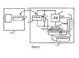
figure 5 représente, de manière schématique, un second mode de réalisation particulier d'un objet portatif selon l'invention, - la
figure 6 représente, de manière plus détaillée, un mode de réalisation particulier correspondant à lafigure 2 , - la
figure 7 représente, de manière plus détaillée, un mode de réalisation particulier correspondant à lafigure 3 .
- the
figure 1 represents, schematically, an embodiment of a portable object according to the prior art, - the
figure 2 represents, schematically, a particular embodiment of a portable object according to the invention, - the
Figures 3 and 4 represent, schematically, two control laws connecting the gain (G) of the control loop to the difference (Err) between a setpoint voltage and a voltage to be regulated, - the
figure 5 represents, schematically, a second particular embodiment of a portable object according to the invention, - the
figure 6 represents, in more detail, a particular embodiment corresponding to thefigure 2 , - the
figure 7 represents, in more detail, a particular embodiment corresponding to thefigure 3 .
Comme illustré à la
De cette manière, la boucle de régulation 6 modifie la tension aux bornes de l'antenne 3 de l'objet portatif, en modulant la valeur de l'impédance Z de charge variable. Cette régulation est classiquement réalisée par rapport à la tension de consigne Vconsigne.In this way, the
Le redresseur 5 peut être réalisé par tout circuit approprié permettant de transformer une tension alternative en une tension continue. Le redresseur peut être par exemple, une diode, un pont de diode, des circuits de redressement mono ou bi-alternance.The
Les moyens 7 de détermination d'une différence Err sont formés, par exemple, par un comparateur dont les première et seconde bornes d'entrée sont connectées respectivement à la tension de consigne Vconsigne et à la tension de sortie Vdb du redresseur 5. La différence Err délivrée par les moyens 7 peut être une tension positive ou négative selon que la tension de sortie Vdb du redresseur est supérieure ou inférieure à la tension de consigne Vconsigne.The
La tension délivrée par les moyens 7 de détermination, c'est-à-dire la différence Err, est ensuite appliquée à une entrée du convertisseur 8 analogique-numérique qui transforme alors cette information analogique en un signal numérique qui est représentatif de la différence Err. Le convertisseur 8 délivre à sa sortie un signal numérique, sur un bit, représentatif de la différence Err entre la tension Vdb et la tension de consigne. Le signal numérique délivré par le convertisseur 8 est appliqué à une entrée des moyens de commande 9.The voltage delivered by the determination means 7, that is to say the difference Err, is then applied to an input of the analog-to-
Le convertisseur 8 analogique-numérique peut être à temps continu, c'est-à-dire qu'il délivre en continue une valeur représentative de la différence entre les tensions appliquées à ses bornes d'entrée, ou alors à temps échantillonné, c'est-à-dire qu'il délivre périodiquement une valeur représentative de la différence elle-même mesurée suivant la même période.The analog-
La boucle de régulation 6 comporte également un gain adaptatif qui est ajusté en fonction de la différence Err entre la tension de consigne et la tension Vdb à la sortie du redresseur. Pour ce faire, les moyens de commande 9 comportent une entrée M de contrôle de gain, connectée à une sortie de moyens 10 de contrôle du gain recevant en entrée des signaux représentatifs de ladite différence Err. L'entrée M peut être décomposée en une pluralité de sous entrée également appelées M.The
Au moyen de la modulation du gain de la boucle de régulation 6, la boucle peut présenter soit un gain élevé, soit un gain plus faible. Dans le cas d'un gain élevé, les oscillations résiduelles sur la tension de sortie Vdb du redresseur sont rejetées à plus haute fréquence ce qui permet d'assurer un bon suivi de la tension de consigne Vconsigne et un rejet des perturbations. Au contraire, si le gain est faible, l'amplitude des oscillations sur la tension de sortie Vdb du redresseur reste faible.By means of the modulation of the gain of the
Les moyens 10 de contrôle du gain définissent une loi de commande qui peut être linéaire ou discrète, dans laquelle le gain G augmente lorsque le signal représentatif, par exemple, la différence Err à l'entrée du convertisseur 8 augmente (
Dans un premier mode de réalisation, illustré à la
Dans un mode de réalisation particulier, correspondant au premier mode de réalisation et illustré à la
Chaque comparateur 11 comporte des première et seconde bornes d'entrée et une borne de sortie. La borne de sortie de chaque comparateur 11 est connectée à une borne de commande d'un interrupteur électronique 12 dont l'une de ses deux bornes d'entrée/sortie est connectée à un générateur de courant 13, la borne restante d'entrée/sortie étant connectée à un circuit intégrateur 18 qui est intégré dans les moyens de commande 9. Les comparateurs 11 sont associés chacun à une tension de référence Ref spécifique. Ainsi, les comparateurs 11 réalisent la comparaison entre la tension de référence Ref et la différence Err et ils délivrent une information numérique (0 ou 1) en conséquence. Les comparateurs 11 associés aux tensions de référence Ref définissent, dans les moyens 10 de contrôle du gain, la loi de commande à appliquer.Each comparator 11 has first and second input terminals and an output terminal. The output terminal of each comparator 11 is connected to a control terminal of an
Ainsi, la
Le mode de réalisation particulier, illustré à la
Avantageusement, la loi de commande étant symétrique par rapport à l'axe des ordonnés (
A titre d'exemple, les comparateurs 11 b et 11b' appartiennent à deux familles différentes. La différence Err entre la tension de consigne et la tension Vdb est appliquée sur la première borne d'entrée du comparateur 11 b alors que la même différence Err est appliquée sur la seconde borne d'entrée du comparateur 11b'. Les tensions de référence associées aux comparateurs 11 b et 11 b' sont identiques en valeur absolue mais opposées en signe, Refb et -Refb.By way of example, the comparators 11b and 11b 'belong to two different families. The difference Err between the setpoint voltage and the voltage Vdb is applied to the first input terminal of the comparator 11b while the same difference Err is applied to the second input terminal of the comparator 11b '. The reference voltages associated with the comparators 11b and 11b 'are identical in absolute value but opposite in sign, Ref b and -Ref b .
De plus, à chaque tension de référence Ref est associée une source de courant I spécifique. De sorte que le comparateur 11b est associé à la tension de référence Refb et à la source 13 de courant Ib par l'intermédiaire d'un interrupteur électronique 12. Pour sa part, le comparateur 11b' est associé à la tension de référence -Refb et à la source de courant -Ib par l'intermédiaire d'un interrupteur électronique. De manière analogue, le comparateur 11i est connecté à la tension de référence Refi et agit sur l'interrupteur électronique relié à la source de courant Ii.In addition, at each reference voltage Ref is associated a specific current source I. So that the comparator 11b is associated with the reference voltage Ref b and the
Ainsi, si la différence Err est comprise entre Refa et Refb, le comparateur 11a délivre en sortie un signal qui actionne la fermeture de l'interrupteur électronique 12a. Il en résulte qu'un courant Ia est appliqué à l'entrée du circuit intégrateur 18, le courant Ia étant proportionnel au gain G1. Si la différence Err est supérieure au moins à Refb, au moins les comparateurs 11a et 11b délivrent chacun en sortie un signal qui actionne la fermeture des interrupteurs électroniques 12a et 12b. Il en résulte alors qu'un courant au moins égale à Ia+Ib est appliqué à l'entrée du circuit 18, le courant Ia+Ib étant proportionnel au gain G2.Thus, if the difference Err is between Refa and Ref b , the
Dans un autre mode de réalisation particulier, non représenté, le comparateur 11b n'est pas utilisé et l'interrupteur et la source de courant qui lui étaient associé sont connectés au signal de la sortie du comparateur 11a, qui a été préalablement transformé en son opposé. Dans ce mode de réalisation, le comparateur 11a appartient toujours au convertisseur 8, mais sa sortie inversée fait partie des moyens 10 de contrôle.In another particular embodiment, not shown, the comparator 11b is not used and the switch and the current source associated therewith are connected to the signal of the output of the
Dans un autre mode de réalisation particulier illustré à la
Dans ce mode de réalisation particulier, les moyens 10 de contrôle du gain comportent une pluralité de bascules 14 de type « flip-flop » ou FF qui sont connectées en série. Chaque bascule 14 « flip-flop » comporte une borne d'entrée de signal, une borne de sortie de signal et une borne d'entrée d'un signal d'horloge ck. La borne d'entrée d'une bascule 14 est connectée à la borne de sortie de la bascule précédente et la borne de sortie de la bascule est connectée à la borne d'entrée de la bascule suivante. De plus, toutes les bornes d'entrée de signal d'horloge sont connectées au même signal d'horloge ck. Les différentes bascules 14 sont donc synchronisées. Ainsi, au fur et à mesure des signaux d'horloges, les bits délivrés par le convertisseur 8 analogique-numérique transitent par les différentes bascules. Sur la
Les bornes de sortie de signal de chaque bascule 14 sont également connectées à un circuit de décodage logique 15. Ce circuit de décodage logique permet de contrôler les variations temporelles du signal numérique représentatif de la différence. Ainsi, si le signal représente une alternance parfaite de 0 et 1, c'est-à-dire d'états hauts et d'états bas, le circuit de décodage délivre un gain minimum. En revanche, plus les écarts à cette alternance sont importants et plus le circuit de décodage délivre un gain important, en fonction de la loi de commande intégrée au circuit de décodage 15 par l'intermédiaire des moyens 10 de commande. Il est également possible et avantageux de prendre en compte la position de l'écart à l'alternance dans le calcul de la valeur du gain. Ainsi, si l'écart à une alternance parfaite est présent à la bascule 14h, le gain sera plus faible que si le même écart est présent à la bascule 14a.The signal output terminals of each flip-flop 14 are also connected to a
L'objet portatif 1 comporte également des moyens 17 de démodulation qui sont connectés entre le convertisseur 8 analogique-numérique et les moyens de commande 9. Les moyens de démodulation utilisent le signal numérique émis par le convertisseur 8 pour traiter l'information contenue dans le champ magnétique H émis depuis la station fixe vers l'objet portatif. Les moyens 17 de démodulation sont connectés au noeud électrique L.The
Dans un autre mode de réalisation qui peut être avantageusement combiné avec les modes de réalisation précédents, la boucle de régulation est partiellement ou totalement désactivée lors de la phase de variation de l'impédance de charge. Cette désactivation permet d'éviter un conflit avec la modulation de l'impédance. La demande de brevet
Dans un mode de réalisation particulier qui peut mis en oeuvre avec ce qui a été décrit précédemment, le circuit peut renvoyer des données de l'objet vers la station fixe. Pour envoyer des données, l'objet portatif modifie l'impédance qu'il présente aux bornes de son antenne. En conséquence, l'impédance rapportée du côté de la station fixe est modifiée. Les données sont alors codées par des variations de charge de l'objet portatif.In a particular embodiment that can be implemented with what has been described above, the circuit can send data from the object to the fixed station. To send data, the portable object modifies the impedance that it presents to the terminals of its antenna. As a result, the impedance reported on the fixed station side is changed. The data is then encoded by load variations of the portable object.
Dans son fonctionnement classique, la boucle de régulation rejette toutes les perturbations qui se présentent aux bornes du circuit. De ce fait, la boucle de régulation entre en conflit avec la variation de charge inhérente au principe de communication par modulation de charge. Il est donc nécessaire de limiter, ou au moins de modifier, l'effet de la boucle de régulation pendant une communication de l'objet portatif vers la station fixe.In its conventional operation, the control loop rejects all the disturbances that occur at the terminals of the circuit. As a result, the regulation loop conflicts with the load variation inherent in the charge modulated communication principle. It is therefore necessary to limit, or at least modify, the effect of the regulation loop during a communication of the portable object to the fixed station.
Cette limitation peut être réaliser, par exemple, en figeant l'état de la boucle de régulation pendant les phases de communication de phase. Cette état figé peut être réalisé en forçant le signal périodique à l'entrée du contrôleur bang-bang. A titre d'exemple, des moyens de coupure du signal, par exemple un interrupteur électronique, sont disposés entre les moyens 7 de détermination de la différence 7 et le convertisseur 8 analogique-numérique. Une fois le convertisseur 8 déconnecté des moyens 7 de détermination, une erreur périodique est appliquée à l'entrée du convertisseur 8 par des moyens d'application d'un signal périodique (non représentés). Durant cette phase, une tension Vshunt constante est appliquée sur l'impédance de charge variable Z.This limitation can be achieved, for example, by setting the state of the control loop during the phases of phase communication. This frozen state can be achieved by forcing the periodic signal at the input of the bang-bang controller. By way of example, means for breaking the signal, for example an electronic switch, are arranged between the
Claims (6)
- A portable object equipped with an antenna (3) inductively coupled to a fixed station (2) of a remote transmission device, the portable object (1) comprising a variable load impedance (Z) connected in parallel to the terminals of the antenna (3) and a rectifier with an input connected to a terminal of the antenna (3), a regulation loop (6) of the voltage at the terminals of the load impedance, connected between the rectifier (5) output and a control terminal of the load impedance (Z), the regulation loop (6) comprising, in series, means (7) for determining a difference between a setpoint voltage (Vconsigne) and the output voltage (Vdb) of the rectifier, a one-bit analog-to-digital converter (8), and command means (9) of integrator type, demodulation means (17) being connected to the converter output (8), object characterized in that the command means (9) are of adjustable gain type and comprise a gain control input (M) connected to an output of the gain control means (10) receiving signals representative of said difference (Err) on input.
- The object according to claim 1, characterized in that the rectifier (5) is connected in parallel to the terminals of the antenna (3)
- The object according to one of the claims 1 and 2, characterized in that said representative signals are the difference (Err) between the setpoint voltage (Vconsigne) and the output voltage (Vdb) of the rectifier (5).
- The object according to one of the claims 1 and 2, characterized in that said representative signals are the difference (Err) between the setpoint voltage (Vconsigne) and the output voltage (Vdb) of the rectifier (5) converted by the analog-to-digital converter (8).
- The object according to claim 4, characterized in that the gain control means (10) comprise means (4, 5) for time integration of the representative signals.
- The object according to any one of the claims 1 to 5, characterized in that it comprises cut-off means of the signal connected between the converter (8) and the means (7) for determining the error, and means for applying a periodic signal to an input of the converter (8).
Applications Claiming Priority (1)
| Application Number | Priority Date | Filing Date | Title |
|---|---|---|---|
| FR0806898A FR2939580A1 (en) | 2008-12-09 | 2008-12-09 | PORTABLE OBJECT INDUCTIVELY COUPLED TO A FIXED STATION AND COMPRISING MEANS FOR CONTROLLING THE GAIN |
Publications (2)
| Publication Number | Publication Date |
|---|---|
| EP2196948A1 EP2196948A1 (en) | 2010-06-16 |
| EP2196948B1 true EP2196948B1 (en) | 2011-10-19 |
Family
ID=40886991
Family Applications (1)
| Application Number | Title | Priority Date | Filing Date |
|---|---|---|---|
| EP09178424A Not-in-force EP2196948B1 (en) | 2008-12-09 | 2009-12-08 | Mobile object inductively coupled to a fixed station and including gain control methods |
Country Status (5)
| Country | Link |
|---|---|
| US (1) | US8369778B2 (en) |
| EP (1) | EP2196948B1 (en) |
| JP (1) | JP5562623B2 (en) |
| AT (1) | ATE529831T1 (en) |
| FR (1) | FR2939580A1 (en) |
Families Citing this family (2)
| Publication number | Priority date | Publication date | Assignee | Title |
|---|---|---|---|---|
| GB2479792B (en) * | 2010-04-23 | 2017-06-14 | Broadcom Innovision Ltd | Near field RF communicator |
| EP2830229B1 (en) | 2013-07-25 | 2017-04-19 | Nxp B.V. | A multichannel transponder and a method of determining a most strongly coupled channel or more strongly coupled channels |
Family Cites Families (6)
| Publication number | Priority date | Publication date | Assignee | Title |
|---|---|---|---|---|
| FR2776865B1 (en) * | 1998-03-31 | 2000-05-05 | Commissariat Energie Atomique | INDUCTIVE COUPLING TELETRANSMISSION DEVICE |
| EP1315292B1 (en) * | 2001-11-21 | 2006-09-13 | Sony Deutschland GmbH | Digital controlled AGC |
| FR2859842B1 (en) * | 2003-09-17 | 2006-02-10 | Commissariat Energie Atomique | PORTABLE MULTINIVE DEMODULATION OBJECT, INDUCTIVELY COUPLED TO A FIXED STATION |
| FR2883433B1 (en) * | 2005-03-21 | 2007-04-20 | Commissariat Energie Atomique | MULTINIVE DEMODULATION METHOD AND DEVICE. |
| JP4206108B2 (en) * | 2006-07-28 | 2009-01-07 | 東芝テック株式会社 | Wireless tag reader / writer |
| DE602007013986D1 (en) * | 2006-10-18 | 2011-06-01 | Semiconductor Energy Lab | ID radio transponder |
-
2008
- 2008-12-09 FR FR0806898A patent/FR2939580A1/en not_active Withdrawn
-
2009
- 2009-11-20 US US12/591,493 patent/US8369778B2/en not_active Expired - Fee Related
- 2009-12-08 AT AT09178424T patent/ATE529831T1/en not_active IP Right Cessation
- 2009-12-08 EP EP09178424A patent/EP2196948B1/en not_active Not-in-force
- 2009-12-09 JP JP2009279630A patent/JP5562623B2/en not_active Expired - Fee Related
Also Published As
| Publication number | Publication date |
|---|---|
| US8369778B2 (en) | 2013-02-05 |
| JP2010154526A (en) | 2010-07-08 |
| JP5562623B2 (en) | 2014-07-30 |
| FR2939580A1 (en) | 2010-06-11 |
| ATE529831T1 (en) | 2011-11-15 |
| US20100144270A1 (en) | 2010-06-10 |
| EP2196948A1 (en) | 2010-06-16 |
Similar Documents
| Publication | Publication Date | Title |
|---|---|---|
| JP4971230B2 (en) | Optical transmitter | |
| EP0654887B1 (en) | Uninterruptible power supply with common neutral line comprising a double boost switching converter | |
| EP2527851B1 (en) | Wireless current sensor | |
| EP0505283B1 (en) | Device for the galvanic insulation of DC electrical signals or signals containing a DC component | |
| EP0052536B1 (en) | Sender module output power stabilization device for an optical fibre transmission system | |
| FR2987521A1 (en) | DEVICE AND METHOD FOR CONTROLLING AN ACTIVE DAMPER CIRCUIT FOR A CONTINUOUS VOLTAGE CONVERTER | |
| EP0004815B1 (en) | System for transmitting optically linked electrical signals and device for the automatic gain control of a receiver path connected to this optical linkage | |
| EP2196948B1 (en) | Mobile object inductively coupled to a fixed station and including gain control methods | |
| EP1104496B1 (en) | Device for access control between electronic key and lock | |
| FR2516323A1 (en) | CIRCUIT FOR CONVERTING AN INFORMATION SIGNAL INTO A RECTANGULAR SIGNAL | |
| EP1665573B1 (en) | Portable object having multi-level demodulation and being inductively coupled to a fixed station | |
| WO1994018520A1 (en) | Mine clearance device | |
| WO1999050930A1 (en) | Device for controlling the impedance returned on an electronic label antenna | |
| KR100997495B1 (en) | Charge control circuit | |
| US20040208645A1 (en) | Method and apparatus for optical transmission of wavelength-encoded modulation formats | |
| EP3726702B1 (en) | Method and system for transmitting the power of a radiofrequency type signal received by a radiofrequency receiver | |
| EP0670624A1 (en) | Switching power supply adapted for allowing reduced voltage commutations | |
| WO2011067513A1 (en) | Dc-dc converter for electric power using a dc electric power source | |
| EP3582385A1 (en) | Dc/dc converter | |
| FR2557399A1 (en) | LINEAR POWER AMPLIFIER | |
| EP1410488B1 (en) | Energy converting device | |
| WO2020021216A1 (en) | Improved sampling device | |
| EP3923477B1 (en) | Device for controlling a switch | |
| EP3139485B1 (en) | Soft starting system for an electrical motor | |
| FR3077912A1 (en) | METHOD OF COMMUNICATION IN AN ELECTRONIC DEVICE FOR CLOSE CONTROL OF AN ELECTRICAL SYSTEM |
Legal Events
| Date | Code | Title | Description |
|---|---|---|---|
| PUAI | Public reference made under article 153(3) epc to a published international application that has entered the european phase |
Free format text: ORIGINAL CODE: 0009012 |
|
| AK | Designated contracting states |
Kind code of ref document: A1 Designated state(s): AT BE BG CH CY CZ DE DK EE ES FI FR GB GR HR HU IE IS IT LI LT LU LV MC MK MT NL NO PL PT RO SE SI SK SM TR |
|
| RAP1 | Party data changed (applicant data changed or rights of an application transferred) |
Owner name: COMMISSARIAT A L'ENERGIE ATOMIQUE ET AUX ENERGIES |
|
| 17P | Request for examination filed |
Effective date: 20101214 |
|
| RIC1 | Information provided on ipc code assigned before grant |
Ipc: G06K 19/00 20060101AFI20110203BHEP Ipc: H04B 5/00 20060101ALI20110203BHEP Ipc: G06K 19/07 20060101ALI20110203BHEP |
|
| GRAP | Despatch of communication of intention to grant a patent |
Free format text: ORIGINAL CODE: EPIDOSNIGR1 |
|
| GRAS | Grant fee paid |
Free format text: ORIGINAL CODE: EPIDOSNIGR3 |
|
| GRAA | (expected) grant |
Free format text: ORIGINAL CODE: 0009210 |
|
| RIN1 | Information on inventor provided before grant (corrected) |
Inventor name: GOMEZ, BERTRAND Inventor name: COLINET, ERIC |
|
| AK | Designated contracting states |
Kind code of ref document: B1 Designated state(s): AT BE BG CH CY CZ DE DK EE ES FI FR GB GR HR HU IE IS IT LI LT LU LV MC MK MT NL NO PL PT RO SE SI SK SM TR |
|
| REG | Reference to a national code |
Ref country code: GB Ref legal event code: FG4D Free format text: NOT ENGLISH |
|
| REG | Reference to a national code |
Ref country code: CH Ref legal event code: EP |
|
| REG | Reference to a national code |
Ref country code: IE Ref legal event code: FG4D |
|
| REG | Reference to a national code |
Ref country code: DE Ref legal event code: R096 Ref document number: 602009003160 Country of ref document: DE Effective date: 20111215 |
|
| REG | Reference to a national code |
Ref country code: NL Ref legal event code: VDEP Effective date: 20111019 |
|
| LTIE | Lt: invalidation of european patent or patent extension |
Effective date: 20111019 |
|
| REG | Reference to a national code |
Ref country code: AT Ref legal event code: MK05 Ref document number: 529831 Country of ref document: AT Kind code of ref document: T Effective date: 20111019 |
|
| PG25 | Lapsed in a contracting state [announced via postgrant information from national office to epo] |
Ref country code: IS Free format text: LAPSE BECAUSE OF FAILURE TO SUBMIT A TRANSLATION OF THE DESCRIPTION OR TO PAY THE FEE WITHIN THE PRESCRIBED TIME-LIMIT Effective date: 20120219 Ref country code: NO Free format text: LAPSE BECAUSE OF FAILURE TO SUBMIT A TRANSLATION OF THE DESCRIPTION OR TO PAY THE FEE WITHIN THE PRESCRIBED TIME-LIMIT Effective date: 20120119 Ref country code: LT Free format text: LAPSE BECAUSE OF FAILURE TO SUBMIT A TRANSLATION OF THE DESCRIPTION OR TO PAY THE FEE WITHIN THE PRESCRIBED TIME-LIMIT Effective date: 20111019 |
|
| REG | Reference to a national code |
Ref country code: IE Ref legal event code: FD4D |
|
| PG25 | Lapsed in a contracting state [announced via postgrant information from national office to epo] |
Ref country code: PT Free format text: LAPSE BECAUSE OF FAILURE TO SUBMIT A TRANSLATION OF THE DESCRIPTION OR TO PAY THE FEE WITHIN THE PRESCRIBED TIME-LIMIT Effective date: 20120220 Ref country code: SI Free format text: LAPSE BECAUSE OF FAILURE TO SUBMIT A TRANSLATION OF THE DESCRIPTION OR TO PAY THE FEE WITHIN THE PRESCRIBED TIME-LIMIT Effective date: 20111019 Ref country code: SE Free format text: LAPSE BECAUSE OF FAILURE TO SUBMIT A TRANSLATION OF THE DESCRIPTION OR TO PAY THE FEE WITHIN THE PRESCRIBED TIME-LIMIT Effective date: 20111019 Ref country code: LV Free format text: LAPSE BECAUSE OF FAILURE TO SUBMIT A TRANSLATION OF THE DESCRIPTION OR TO PAY THE FEE WITHIN THE PRESCRIBED TIME-LIMIT Effective date: 20111019 Ref country code: HR Free format text: LAPSE BECAUSE OF FAILURE TO SUBMIT A TRANSLATION OF THE DESCRIPTION OR TO PAY THE FEE WITHIN THE PRESCRIBED TIME-LIMIT Effective date: 20111019 Ref country code: GR Free format text: LAPSE BECAUSE OF FAILURE TO SUBMIT A TRANSLATION OF THE DESCRIPTION OR TO PAY THE FEE WITHIN THE PRESCRIBED TIME-LIMIT Effective date: 20120120 Ref country code: NL Free format text: LAPSE BECAUSE OF FAILURE TO SUBMIT A TRANSLATION OF THE DESCRIPTION OR TO PAY THE FEE WITHIN THE PRESCRIBED TIME-LIMIT Effective date: 20111019 |
|
| PG25 | Lapsed in a contracting state [announced via postgrant information from national office to epo] |
Ref country code: CY Free format text: LAPSE BECAUSE OF FAILURE TO SUBMIT A TRANSLATION OF THE DESCRIPTION OR TO PAY THE FEE WITHIN THE PRESCRIBED TIME-LIMIT Effective date: 20111019 |
|
| BERE | Be: lapsed |
Owner name: COMMISSARIAT A L'ENERGIE ATOMIQUE ET AUX ENERGIES Effective date: 20111231 |
|
| PG25 | Lapsed in a contracting state [announced via postgrant information from national office to epo] |
Ref country code: CZ Free format text: LAPSE BECAUSE OF FAILURE TO SUBMIT A TRANSLATION OF THE DESCRIPTION OR TO PAY THE FEE WITHIN THE PRESCRIBED TIME-LIMIT Effective date: 20111019 Ref country code: SK Free format text: LAPSE BECAUSE OF FAILURE TO SUBMIT A TRANSLATION OF THE DESCRIPTION OR TO PAY THE FEE WITHIN THE PRESCRIBED TIME-LIMIT Effective date: 20111019 Ref country code: IE Free format text: LAPSE BECAUSE OF FAILURE TO SUBMIT A TRANSLATION OF THE DESCRIPTION OR TO PAY THE FEE WITHIN THE PRESCRIBED TIME-LIMIT Effective date: 20111019 Ref country code: DK Free format text: LAPSE BECAUSE OF FAILURE TO SUBMIT A TRANSLATION OF THE DESCRIPTION OR TO PAY THE FEE WITHIN THE PRESCRIBED TIME-LIMIT Effective date: 20111019 Ref country code: BG Free format text: LAPSE BECAUSE OF FAILURE TO SUBMIT A TRANSLATION OF THE DESCRIPTION OR TO PAY THE FEE WITHIN THE PRESCRIBED TIME-LIMIT Effective date: 20120119 Ref country code: MC Free format text: LAPSE BECAUSE OF NON-PAYMENT OF DUE FEES Effective date: 20111231 Ref country code: EE Free format text: LAPSE BECAUSE OF FAILURE TO SUBMIT A TRANSLATION OF THE DESCRIPTION OR TO PAY THE FEE WITHIN THE PRESCRIBED TIME-LIMIT Effective date: 20111019 |
|
| PLBE | No opposition filed within time limit |
Free format text: ORIGINAL CODE: 0009261 |
|
| STAA | Information on the status of an ep patent application or granted ep patent |
Free format text: STATUS: NO OPPOSITION FILED WITHIN TIME LIMIT |
|
| PG25 | Lapsed in a contracting state [announced via postgrant information from national office to epo] |
Ref country code: PL Free format text: LAPSE BECAUSE OF FAILURE TO SUBMIT A TRANSLATION OF THE DESCRIPTION OR TO PAY THE FEE WITHIN THE PRESCRIBED TIME-LIMIT Effective date: 20111019 Ref country code: RO Free format text: LAPSE BECAUSE OF FAILURE TO SUBMIT A TRANSLATION OF THE DESCRIPTION OR TO PAY THE FEE WITHIN THE PRESCRIBED TIME-LIMIT Effective date: 20111019 Ref country code: IT Free format text: LAPSE BECAUSE OF FAILURE TO SUBMIT A TRANSLATION OF THE DESCRIPTION OR TO PAY THE FEE WITHIN THE PRESCRIBED TIME-LIMIT Effective date: 20111019 |
|
| 26N | No opposition filed |
Effective date: 20120720 |
|
| PG25 | Lapsed in a contracting state [announced via postgrant information from national office to epo] |
Ref country code: BE Free format text: LAPSE BECAUSE OF NON-PAYMENT OF DUE FEES Effective date: 20111231 |
|
| REG | Reference to a national code |
Ref country code: DE Ref legal event code: R097 Ref document number: 602009003160 Country of ref document: DE Effective date: 20120720 |
|
| PG25 | Lapsed in a contracting state [announced via postgrant information from national office to epo] |
Ref country code: AT Free format text: LAPSE BECAUSE OF FAILURE TO SUBMIT A TRANSLATION OF THE DESCRIPTION OR TO PAY THE FEE WITHIN THE PRESCRIBED TIME-LIMIT Effective date: 20111019 |
|
| PG25 | Lapsed in a contracting state [announced via postgrant information from national office to epo] |
Ref country code: MT Free format text: LAPSE BECAUSE OF FAILURE TO SUBMIT A TRANSLATION OF THE DESCRIPTION OR TO PAY THE FEE WITHIN THE PRESCRIBED TIME-LIMIT Effective date: 20111019 Ref country code: MK Free format text: LAPSE BECAUSE OF FAILURE TO SUBMIT A TRANSLATION OF THE DESCRIPTION OR TO PAY THE FEE WITHIN THE PRESCRIBED TIME-LIMIT Effective date: 20111019 |
|
| PG25 | Lapsed in a contracting state [announced via postgrant information from national office to epo] |
Ref country code: SM Free format text: LAPSE BECAUSE OF FAILURE TO SUBMIT A TRANSLATION OF THE DESCRIPTION OR TO PAY THE FEE WITHIN THE PRESCRIBED TIME-LIMIT Effective date: 20111019 Ref country code: ES Free format text: LAPSE BECAUSE OF FAILURE TO SUBMIT A TRANSLATION OF THE DESCRIPTION OR TO PAY THE FEE WITHIN THE PRESCRIBED TIME-LIMIT Effective date: 20120130 |
|
| PG25 | Lapsed in a contracting state [announced via postgrant information from national office to epo] |
Ref country code: LU Free format text: LAPSE BECAUSE OF NON-PAYMENT OF DUE FEES Effective date: 20111208 |
|
| PG25 | Lapsed in a contracting state [announced via postgrant information from national office to epo] |
Ref country code: FI Free format text: LAPSE BECAUSE OF FAILURE TO SUBMIT A TRANSLATION OF THE DESCRIPTION OR TO PAY THE FEE WITHIN THE PRESCRIBED TIME-LIMIT Effective date: 20111019 |
|
| PG25 | Lapsed in a contracting state [announced via postgrant information from national office to epo] |
Ref country code: TR Free format text: LAPSE BECAUSE OF FAILURE TO SUBMIT A TRANSLATION OF THE DESCRIPTION OR TO PAY THE FEE WITHIN THE PRESCRIBED TIME-LIMIT Effective date: 20111019 |
|
| PG25 | Lapsed in a contracting state [announced via postgrant information from national office to epo] |
Ref country code: HU Free format text: LAPSE BECAUSE OF FAILURE TO SUBMIT A TRANSLATION OF THE DESCRIPTION OR TO PAY THE FEE WITHIN THE PRESCRIBED TIME-LIMIT Effective date: 20111019 |
|
| REG | Reference to a national code |
Ref country code: CH Ref legal event code: PL |
|
| PG25 | Lapsed in a contracting state [announced via postgrant information from national office to epo] |
Ref country code: LI Free format text: LAPSE BECAUSE OF NON-PAYMENT OF DUE FEES Effective date: 20131231 Ref country code: CH Free format text: LAPSE BECAUSE OF NON-PAYMENT OF DUE FEES Effective date: 20131231 |
|
| PGFP | Annual fee paid to national office [announced via postgrant information from national office to epo] |
Ref country code: GB Payment date: 20141218 Year of fee payment: 6 |
|
| REG | Reference to a national code |
Ref country code: FR Ref legal event code: PLFP Year of fee payment: 7 |
|
| GBPC | Gb: european patent ceased through non-payment of renewal fee |
Effective date: 20151208 |
|
| PG25 | Lapsed in a contracting state [announced via postgrant information from national office to epo] |
Ref country code: GB Free format text: LAPSE BECAUSE OF NON-PAYMENT OF DUE FEES Effective date: 20151208 |
|
| REG | Reference to a national code |
Ref country code: FR Ref legal event code: PLFP Year of fee payment: 8 |
|
| REG | Reference to a national code |
Ref country code: FR Ref legal event code: PLFP Year of fee payment: 9 |
|
| PGFP | Annual fee paid to national office [announced via postgrant information from national office to epo] |
Ref country code: DE Payment date: 20191216 Year of fee payment: 11 |
|
| PGFP | Annual fee paid to national office [announced via postgrant information from national office to epo] |
Ref country code: FR Payment date: 20191231 Year of fee payment: 11 |
|
| REG | Reference to a national code |
Ref country code: DE Ref legal event code: R119 Ref document number: 602009003160 Country of ref document: DE |
|
| PG25 | Lapsed in a contracting state [announced via postgrant information from national office to epo] |
Ref country code: FR Free format text: LAPSE BECAUSE OF NON-PAYMENT OF DUE FEES Effective date: 20201231 |
|
| PG25 | Lapsed in a contracting state [announced via postgrant information from national office to epo] |
Ref country code: DE Free format text: LAPSE BECAUSE OF NON-PAYMENT OF DUE FEES Effective date: 20210701 |