EP2196142A1 - Electrode sheet and process for producing electrode sheet - Google Patents
Electrode sheet and process for producing electrode sheet Download PDFInfo
- Publication number
- EP2196142A1 EP2196142A1 EP08833687A EP08833687A EP2196142A1 EP 2196142 A1 EP2196142 A1 EP 2196142A1 EP 08833687 A EP08833687 A EP 08833687A EP 08833687 A EP08833687 A EP 08833687A EP 2196142 A1 EP2196142 A1 EP 2196142A1
- Authority
- EP
- European Patent Office
- Prior art keywords
- electrode sheet
- electrode
- wiring layer
- sheet according
- carbon nanotubes
- Prior art date
- Legal status (The legal status is an assumption and is not a legal conclusion. Google has not performed a legal analysis and makes no representation as to the accuracy of the status listed.)
- Withdrawn
Links
Images


Classifications
-
- A—HUMAN NECESSITIES
- A61—MEDICAL OR VETERINARY SCIENCE; HYGIENE
- A61B—DIAGNOSIS; SURGERY; IDENTIFICATION
- A61B5/00—Measuring for diagnostic purposes; Identification of persons
- A61B5/24—Detecting, measuring or recording bioelectric or biomagnetic signals of the body or parts thereof
- A61B5/25—Bioelectric electrodes therefor
- A61B5/251—Means for maintaining electrode contact with the body
- A61B5/257—Means for maintaining electrode contact with the body using adhesive means, e.g. adhesive pads or tapes
- A61B5/259—Means for maintaining electrode contact with the body using adhesive means, e.g. adhesive pads or tapes using conductive adhesive means, e.g. gels
-
- A—HUMAN NECESSITIES
- A61—MEDICAL OR VETERINARY SCIENCE; HYGIENE
- A61B—DIAGNOSIS; SURGERY; IDENTIFICATION
- A61B5/00—Measuring for diagnostic purposes; Identification of persons
- A61B5/24—Detecting, measuring or recording bioelectric or biomagnetic signals of the body or parts thereof
- A61B5/25—Bioelectric electrodes therefor
- A61B5/279—Bioelectric electrodes therefor specially adapted for particular uses
- A61B5/28—Bioelectric electrodes therefor specially adapted for particular uses for electrocardiography [ECG]
- A61B5/282—Holders for multiple electrodes
-
- A—HUMAN NECESSITIES
- A61—MEDICAL OR VETERINARY SCIENCE; HYGIENE
- A61B—DIAGNOSIS; SURGERY; IDENTIFICATION
- A61B5/00—Measuring for diagnostic purposes; Identification of persons
- A61B5/68—Arrangements of detecting, measuring or recording means, e.g. sensors, in relation to patient
- A61B5/6801—Arrangements of detecting, measuring or recording means, e.g. sensors, in relation to patient specially adapted to be attached to or worn on the body surface
- A61B5/6802—Sensor mounted on worn items
- A61B5/6804—Garments; Clothes
-
- A—HUMAN NECESSITIES
- A61—MEDICAL OR VETERINARY SCIENCE; HYGIENE
- A61B—DIAGNOSIS; SURGERY; IDENTIFICATION
- A61B5/00—Measuring for diagnostic purposes; Identification of persons
- A61B5/68—Arrangements of detecting, measuring or recording means, e.g. sensors, in relation to patient
- A61B5/6801—Arrangements of detecting, measuring or recording means, e.g. sensors, in relation to patient specially adapted to be attached to or worn on the body surface
- A61B5/683—Means for maintaining contact with the body
- A61B5/6832—Means for maintaining contact with the body using adhesives
- A61B5/6833—Adhesive patches
-
- A—HUMAN NECESSITIES
- A61—MEDICAL OR VETERINARY SCIENCE; HYGIENE
- A61B—DIAGNOSIS; SURGERY; IDENTIFICATION
- A61B2562/00—Details of sensors; Constructional details of sensor housings or probes; Accessories for sensors
- A61B2562/12—Manufacturing methods specially adapted for producing sensors for in-vivo measurements
- A61B2562/125—Manufacturing methods specially adapted for producing sensors for in-vivo measurements characterised by the manufacture of electrodes
-
- Y—GENERAL TAGGING OF NEW TECHNOLOGICAL DEVELOPMENTS; GENERAL TAGGING OF CROSS-SECTIONAL TECHNOLOGIES SPANNING OVER SEVERAL SECTIONS OF THE IPC; TECHNICAL SUBJECTS COVERED BY FORMER USPC CROSS-REFERENCE ART COLLECTIONS [XRACs] AND DIGESTS
- Y10—TECHNICAL SUBJECTS COVERED BY FORMER USPC
- Y10T—TECHNICAL SUBJECTS COVERED BY FORMER US CLASSIFICATION
- Y10T29/00—Metal working
- Y10T29/49—Method of mechanical manufacture
- Y10T29/49002—Electrical device making
- Y10T29/49117—Conductor or circuit manufacturing
- Y10T29/49124—On flat or curved insulated base, e.g., printed circuit, etc.
- Y10T29/49155—Manufacturing circuit on or in base
-
- Y—GENERAL TAGGING OF NEW TECHNOLOGICAL DEVELOPMENTS; GENERAL TAGGING OF CROSS-SECTIONAL TECHNOLOGIES SPANNING OVER SEVERAL SECTIONS OF THE IPC; TECHNICAL SUBJECTS COVERED BY FORMER USPC CROSS-REFERENCE ART COLLECTIONS [XRACs] AND DIGESTS
- Y10—TECHNICAL SUBJECTS COVERED BY FORMER USPC
- Y10T—TECHNICAL SUBJECTS COVERED BY FORMER US CLASSIFICATION
- Y10T442/00—Fabric [woven, knitted, or nonwoven textile or cloth, etc.]
- Y10T442/20—Coated or impregnated woven, knit, or nonwoven fabric which is not [a] associated with another preformed layer or fiber layer or, [b] with respect to woven and knit, characterized, respectively, by a particular or differential weave or knit, wherein the coating or impregnation is neither a foamed material nor a free metal or alloy layer
- Y10T442/2418—Coating or impregnation increases electrical conductivity or anti-static quality
Definitions
- the present invention relates to an electrode for use to measure an electrocardiographic waveform or the like, and in particular to the improvement of wiring for an electrode and so forth.
- Biological information including an electrocardiogram is occasionally measured in emergencies such as in an ambulance.
- a measuring person attaches an electrode to each of the chest, wrists, and ankles of a person to be measured by suction, and then takes an electrocardiogram using an electrocardiogram measurement device.
- the electrocardiogram measurement according to the proir art requires much time to attach electrodes by suction, and thus may not be suitable for use in emergencies.
- a large number of wiring cords which are connected to a large number of electrodes are occasionally tangled with each other to lower the working efficiency.
- Patent Document 1 discloses a technique in which electrodes are provided to a garment such as a T-shirt.
- Patent Document 2 discloses a technique in which a metal layer is provided on a surface of a fabric by plating or vapor deposition to maintain the conductivity of a wiring layer provided on the fabric to be high.
- Patent Document 1 JP-A-2002-159458
- Patent Document 2 JP-A-1992(Hei4)-108168
- Patent Document 1 While the prior art according to Patent Document 1 above facilitates mounting of the electrodes, however, the conductivity of wiring provided on a fabric is low.
- Patent Document 2 successfully addresses the above issues, providing a metal layer on a surface of a fabric by plating or vapor deposition is not easy and complicates the production process.
- composition of a conductive ink to be printed on a surface of a fabric which has significant projections and depressions, is particularly discussed in neither of the above prior art documents.
- the lower insulating layer as an underlayer for the wiring layer, it is possible to form the wiring layer on a flatter surface, and to ensure the conductivity.
- electrode sheet refers to a sheet having an electrode that measures biological information such as an electrocardiogram, an electromyogram, and an electroencephalogram, and that may include not only sheets having a flat shape but also those having a three-dimensional shape that conforms to the shape of a body and those having a ring shape.
- material refers to a carrier that is provided with an electrode and a wiring layer, and that may include not only woven or knit materials but also thin flexible sheets made of rubber, plastic, or the like.
- FIG. 1 shows the appearance of an electrode sheet 1 for electrocardiogram measurement according to an embodiment of the present invention.
- chest electrodes E3, E4, ... , E8 , neutral electrodes T1, T2, T9, and T10, and wiring layers L1, L2, ..., L10 are formed on a material 2.
- the chest electrodes E3, E4, ..., E8 and the neutral electrodes T1, T2, T9, and T10 for electrocardiogram measurement are formed of an adhesive conductive paste.
- FIG. 2A shows a cross-sectional view taken along the line IIA-IIA of FIG. 1 .
- a lower insulating layer 4 made from an insulating ink is formed on the material 2, and the wiring layer L1 made from a conductive ink is formed on the lower insulating layer 4.
- the neutral electrode T1 is formed on the wiring layer L1.
- the other electrode portions are configured in the same manner.
- the material 2 is preferably formed by knitting to provide elasticity.
- the insulating ink forming the lower insulating layer 4 is made from an acrylic material.
- the conductive ink forming the wiring layer L1 is obtained by mixing carbon nanotubes (5% to 10% by weight), a dispersant, and a binder.
- the conductive paste forming the chest electrodes E3, E4, ..., E8 and the neutral electrodes T1, T2, T9, and T10 is made from silver/silver chloride (ST-gel, manufactured by Sekisui Plastics Co., Ltd.).
- a conductive ink containing carbon nanotubes is used because it keeps providing conductivity to the wiring layer with the elongated carbon nanotubes tangled with each other even when the material is stretched.
- the carbon nanotubes are preferably long. In consideration of ease of manufacture, the carbon nanotubes are preferably 80 ⁇ m to 150 ⁇ m long. More preferably, the carbon nanotubes are 100 ⁇ m to 120 ⁇ m long. While single-layer carbon nanotubes may be used, multi-layer carbon nanotubes are preferably used in consideration of conductivity. While the single-layer carbon nanotubes generally have a diameter of 0.5nm to 5 nm, the multi-layer carbon nanotubes generally have a diameter of 10nm to 100 nm. In the embodiment, multi-layer carbon nanotubes manufactured by an arc discharge method are used.
- the carbon nanotubes are highly cohesive.
- a dispersant is used to disperse the carbon nanotubes as uniformly as possible.
- an acrylic acid polymer for example, a polymer of acrylic acid and amide acrylate
- the dispersant include a nonionic polymer surfactant (for example, a polyester type, a Pluronic type, a tetranic type, an acrylic type, and so forth).
- a binder composed of a flexible material is used to organize the carbon nanotubes in a certain form so that it keeps them in shape to a certain degree even in the case where the material is stretched or shrunk.
- a binder containing an acrylic resin for example, a polymer or a copolymer containing one of methacrylic ester, acrylic ester, and ethyl acrylate as the main component
- the binder include a polyester resin, a urethane resin, or a silicone resin.
- FIG. 2B shows a cross-sectional view taken along the line IIB-IIB of FIG. 1 .
- FIG. 2B is the same as FIG. 2A in that the lower insulating layer 4 made from an insulating ink is formed on the material 2, and the wiring layer L1 made from a conductive ink is formed on the lower insulating layer 4.
- An upper insulating layer 8 made from an insulating ink is formed on the wiring layer L1.
- the other wiring layers are structured in the same manner.
- the upper insulating layer 8 covers the wiring layers L1, L2, ... , L10 so that no conductive portions other than the chest electrodes E3, E4, ... , E8 and the neutral electrodes T1, T2, T9, and T10 contact a human body. This enables accurate measurement of an electrocardiogram.
- FIG. 2C shows a partial cross-sectional view taken along the line IIC-IIC of FIG. 1 .
- the lower insulating layer 4 made from an insulating ink is formed on the material 2, and the wiring layers L1, L2, ..., L10 made from a conductive ink are selectively formed on the lower insulating layer 4.
- the film substrate 10 is formed by printed wires P1, P2, ..., P10 on an insulating flexible film 14.
- the wires P1, P2, ..., P10 are respectively provided at positions corresponding to the wiring layers L1, L2, ..., L10.
- the film substrate 10 and the material 2 are secured to each other by an adhesive 18 with each of the wires P1, P2, ..., P10 of the film substrate 10 contacting the corresponding one of the wiring layers L1, L2, ..., L10.
- the insulating adhesive 18 is provided at portions other than the wires P1, P2, ..., P10 and the wiring layers L1, L2, ..., L10.
- the film substrate 10 is provided with the connector 12 that is connectable to an external device (such as an electrocardiograph).
- an external device such as an electrocardiograph
- the contact resistance between the skin of a human body and the electrodes can be about several M ⁇ .
- a resistance value, from one end (electrode portion) of the wiring layer to the other end (connector portion), of 1000 K ⁇ or less is sufficient for practical use when the material is stretched by about 30%.
- the resistance value is preferably 100 K ⁇ , more preferably 10K ⁇ .
- the electrode sheet 1 is used with the chest electrodes E3, E4, ..., E8 and the neutral electrodes T1, T2, T9, and T10 sticking to a human body.
- Each of the electrodes is formed of an adhesive conductive paste to be suitable for sticking.
- the material 2 may be slackened or stretched to dispose each of the electrodes at a desired position.
- a device-side connector 16 that is connectable to an electrocardiograph is connected to the connector 12. This allows measurement of an electrocardiogram with the electrocardiograph.
- the use of the electrode sheet eliminates the risk that the wires from the electrodes are tangled with each other, and allows quick preparation for measurement with the electrodes roughly disposed in position previously.
- a blended yarn of polyester and urethane is used as the fibers of the shirt.
- a blended yarn with about one fifth (preferably 18%) of urethane with respect to polyester is used.
- Such a yarn is knit to form the material of the shirt. Urethane which has high elasticity itself is knit to obtain much higher elasticity.
- any natural or synthetic fibers other than those described above may be used as the fibers of the shirt.
- materials obtained by knitting or weaving non-blended polyester, non-blended urethane, non-blended nylon, non-blended cotton, non-blended acryl, or a blended yarn of these may be used.
- materials obtained by knitting or weaving various natural fibers such as cotton and wool may also be used. These fibers may be blended at any proportion to obtain the material.
- a knit material is preferable where the elasticity is important, a woven material or a nonwoven material may also be used.
- the above material is heated at around 200 degrees Celsius (for example, 196 degrees Celsius). This eliminates distortion to stabilize the shape of the material.
- the material is immersed in a hot dye solution to dye the material.
- the process may be omitted.
- the material is heated again at around 170 degrees (for example, 160 degrees) Celsius to adjust the dimensions.
- Smoothing refers to a process in which projections and depressions formed by loops on a surface of the material are flattened using heat or pressure to smooth the surface compared to that before the process.
- smoothing is performed using a calendering process.
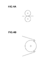
- calendering machines as shown in FIGs. 4A and 4B may be used.
- a material with a width of 100 to 220 cm is subjected to a linear pressure of 20 tons to 50 tons using rollers at temperatures of 190 to 200 degrees Celsius.
- the surface of the material changes from a state with significant projections and depressions as shown in FIG. 5A into a relatively flat state as shown in FIG. 5B .
- the lower insulating layer 4 is printed with an insulating ink as an underlayer for each of the wiring layers L1, L2, ..., L10.
- An acrylic resin for example, a binder EN-ME/EN-MRE manufactured by Matsui Shikiso Chemical Co., Ltd.
- a urethane resin or the like may also be used.
- the lower insulating layer 4 is wider than each of the wiring layers L1, L2, ..., L10 by 1 mm to several mm. This allows each of the wiring layers L1, L2, ..., L10 to be placed on the lower insulating layer 4 even if the wiring layers L1, L2, ..., L10 are printed in a displaced manner.
- the conductive ink for the wiring layers L1, L2, ..., L10 is obtained by compounding carbon nanotubes, a dispersant, and a binder.
- An amphipathic acrylic polymer (a polymer of acrylic acid and amide acrylate, which may be TX-17-100 manufactured by Kyoeisha Chemical Co., Ltd., for example) is used as the dispersant.
- An acrylic soft binder (a polymer of acrylic ester, which may be Light Epoch T-23M manufactured by Kyoeisha Chemical Co., Ltd., for example) is used as the binder.
- the compounding ratios of the amphipathic acrylic polymer, the acrylic soft binder, and the carbon nanotubes are respectively 0.5 to 2.0% by weight, 5 to 8% by weight, and 5 to 10% by weight, with the remaining component being water.
- Tables 1 and 2 show variations in conductivity with the carbon nanotubes compounded at various ratios.
- Table 1 corresponds to a case where printing is performed on the front surface of the material.
- Table 2 corresponds to a case where printing is performed on the back surface of the material.
- TX17-1 and TX17-1A are obtained by compounding 0.85% by weight of the amphipathic acrylic polymer (dispersant), 5.8% by weight of the acrylic soft binder, and 5.0% of the carbon nanotubes.
- multi-layer carbon nanotubes with a diameter of 150 nm and a length of 10 to 20 ⁇ m are used as the carbon nanotubes.
- TX17-1B is obtained by compounding 1.6% by weight of the amphipathic acrylic polymer (dispersant), 7.2% by weight of the acrylic soft binder, and 8.3% of the carbon nanotubes.
- TX17-1C is obtained by compounding 1.7% by weight of the amphipathic acrylic polymer (dispersant), 5.6% by weight of the acrylic soft binder, and 8.9% of the carbon nanotubes.
- the conductive ink may include other conductive materials or ink such as silver particles in addition to or in place of the carbon nanotubes.
- the upper insulating layer 8 is printed with an insulating ink on each of the wiring layers L1, L2, ..., L10.
- the material of the insulating ink used to form the upper insulating layer is the same as the material of the insulating ink used to form the lower insulating layer.
- the upper insulating layer 8 is formed to be wider than each of the wiring layers L1, L2, ..., L10 by 1 mm to several mm so as to reliably cover each of the wiring layers L1, L2, ..., L10 even if printing is performed in a more or less displaced manner.
- the upper insulating layer 8 is not printed on portions at which the chest electrodes E3, E4, ..., E8 and the neutral electrodes T1, T2, T9, and T10 are to be formed and on a portion to which the film substrate 10 is to be jointed.
- a hot-melt adhesive is printed to join the wiring layers L1, L2, ..., L10 to the film substrate 10.
- the hot-melt adhesive is printed at portions in the vicinity of the wiring layers L1, L2, ..., L10 and not on the wiring layers L1, L2, ..., L10.
- a mixture of an acrylic ester copolymer resin, ethylene glycol, water, and so forth (for example, a binder K-2050 manufactured by Meisei Chemical Works, Ltd.) is used as the hot-melt adhesive.
- the upper insulating layer 8, the wiring layers L, the lower insulating layer 4, and the hot-melt adhesive are printed using hand printing in the embodiment, they may be printed using automatic printing, rotary printing, inkjet printing, or the like.
- the entire material 2 is heated at about 150 degrees Celsius to promote curing of the upper insulating layer 8 for sufficient insulation.
- a conductive paste is pasted on electrode portions of the wiring layers L1, L2, ..., L10.
- Silver/silver chloride ST-gel, manufactured by Sekisui Plastics Co., Ltd.
- ST-gel manufactured by Sekisui Plastics Co., Ltd.
- the film substrate 10 with the connector 12 shown in FIG. 7 is placed on portions at which the hot-melt adhesive is printed as shown in FIG. 6 .
- the film substrate 10 is positioned such that the wires P1, P2, ..., P10 respectively oppose and contact the wiring layers L1, L2, ..., L10.
- the hot-melt adhesive is heated at 80 degrees to 150 degrees to be dissolved for adhesion using a small-sized transfer machine, and then is cooled to be cured. This allows the film substrate 10 to adhere to the material 2.
- the present invention is implemented as the electrode sheet 1.
- the chest electrodes E3, E4, ..., E8, the neutral electrodes T1, T2, T9, and T10, and the wiring layers L1, L2, ..., L10 may be provided on the inner side (the side that contacts the skin) of a garment such as a shirt.
- preparation for placement of the electrodes for electrocardiogram measurement can be performed by wearing the shirt.
- the chest electrodes E3, E4, ..., E8 may not be disposed in correct position depending on differences among individual wearers.
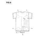
- the chest electrodes E3, E4, ..., E8 are elongated vertically as shown in FIG. 8 so as to allow accurate measurement even if the electrodes are displaced.
- the electrodes are formed from an adhesive material.
- an insulating adhesive may be pasted to desired portions other than the electrodes to improve adhesion of the electrode sheet to a human body.
- the material has the shape of a flat sheet in the above embodiment, the material may have the shape of a thin sheet that conforms to the shape of a body or have the shape of a ring (like a belly band).
- the material is a woven or knit cloth.
- the material may be a thin flexible sheet made of rubber, plastic, or the like.
- a material formed by knitting a blended yarn of polyester and urethane was used to measure electrical resistance values.
- the percentages of polyester fibers and urethane fibers were respectively 82% and 18%.
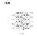
- FIG. 10 shows a knitting structure of the material.
- the material was formed of front yarns and back yarns.
- the front yarns and the back yarns are respectively indicated by the thick lines and the thin lines.
- a lower insulating layer in a pattern as shown in FIG. 9 was printed on the front surface or the back surface of the material, and wiring layers were printed on the lower insulating layer.
- An acrylic resin (a binder EN-ME/EN-MRE manufactured by Matsui Shikiso Chemical Co., Ltd.) was used as the insulating ink forming the lower insulating layer.
- the conductive ink forming the wiring layers was obtained by compounding carbon nanotubes, a dispersant, and a binder.
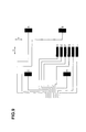
- the "Left” in the “Location” field indicates a measurement performed at the wiring layer connected to the electrode B in FIG. 9 .
- the “Center” indicates a measurement performed at a wiring layer connected to the electrode E.
- the “Right” indicates a measurement performed at a wiring layer connected to the electrode J.
- the “Vertical” in the “Knitting direction” field refers to a direction in which the knit yarn is continuous. It corresponds to the Y direction in FIG. 10 .
- the measurements were performed in the Y direction in FIG. 9 corresponding to the vertical knitting direction.
- the “Horizontal” in the "Knitting direction” field refers to a direction in which the knit yarn is not continuous. It corresponds to the X direction in FIG. 10 .
- the measurements were performed in the X direction in FIG. 9 corresponding to the horizontal knitting direction.
- Tables 3 to 6 show measurement values for a case where the calendering process was not performed.
- Tables 3 and 5 correspond to a case where the wiring layers were printed on the front surface of the material.
- Tables 4 and 6 correspond to a case where the wiring layers were printed on the back surface of the material.
- the front surface and the back surface of the material respectively mean a sinker surface and a needle surface.
- Tables 5 and 6 show the results of measuring a resistance value over the entire length of the wire for each electrode.
- Terminal Electrical resistance Average A 500 or more 500 or more B 500 or more C 500 or more D 500 or more E 500 or more F 500 or more G 500 or more H 500 or more I 500 or more J 500 or more
- Tables 7 to 10 show measurement values for a case where a calendering process was performed.
- Tables 7 and 9 correspond to a case where the wiring layers were printed on the front surface of the material.
- Tables 8 and 10 correspond to a case where the wiring layers were printed on the back surface of the material.
- Tables 9 and 10 show the results of measuring a resistance value over the entire length of the wire for each electrode.
- the conductivity was improved by the calendering process. Moreover, the conductivity was higher in the "vertical" "knitting direction” than the "horizontal” knitting direction, and was higher on the back surface than the front surface. Thus, it is preferable to print the wiring layers using the back surface and such that the direction of the wiring layers matches the vertical knitting direction as much as possible. For example, if the wires as shown in FIG. 9 are formed, it is preferable that the X direction in the drawing corresponds to the "vertical" "knitting direction”.
- Table 11 shows the results of measuring variations in resistance value in wiring layers in the case where the material was stretched.
- the conductive ink 1.7% (by weight) of an amphipathic acrylic polymer (TX-17-100 manufactured by Kyoeisha Chemical Co., Ltd.) serving as the dispersant, 5.1% (by weight) of an acrylic soft binder (Light Epoch T-23M manufactured by Kyoeisha Chemical Co., Ltd.) serving as the binder, and 9.5% by weight of multi-layer carbon nanotubes (with a diameter of 150 nm and a length of 10 to 20 ⁇ m) were compounded.
- TX-17-100 manufactured by Kyoeisha Chemical Co., Ltd.
- an acrylic soft binder Light Epoch T-23M manufactured by Kyoeisha Chemical Co., Ltd.
- Wiring layers with a width of 4 mm and a length of 10 cm were formed using the above conductive ink in each of the X direction and the Y direction shown in FIG. 10 . Resistance values were measured for the entire length of the wiring layer formed in the X direction in cases where the wiring layer was not stretched, stretched by 30%, and stretched by 50%. The same measurements were performed on the wiring layer formed in the Y direction. The wiring layers were printed after a calendering process was performed on the front surface of the material.
- the resistance value of the wiring layer in the X direction was unstable and thus could not be measured although the resistance value of the wiring layer in the Y direction remained in the order of K ⁇ .
- Table 12 shows the results of testing the adhesive strength in cases where the material of the film substrate and the component of the hot-melt adhesive were varied. In the tests, an acrylic ester copolymer resin and a nylon resin were used as the component of the hot-melt adhesive, while a polyester film and a polyimide film were used as the material of the film substrate. A thermal transfer machine was used to perform an adhesion process at 150 degrees for 20 seconds.
- the adhesive strength was highest in the case where a polyimide film was used as the film substrate and a nylon resin was used as the hot-melt adhesive.
- a lower insulating layer in a pattern as shown in FIG. 11 was printed on a material formed by knitting a blended yarn of polyester and urethane and wiring layers with a width of 0.4 cm and a thickness of 0.02 to 03 cm were printed on the lower insulating layer.
- the percentages of polyester fibers and urethane fibers were respectively 82% and 18%.
- An acrylic resin (a binder EN-ME/EN-MRE manufactured by Matsui Shikiso Chemical Co., Ltd.) was used as the insulating ink forming the lower insulating layer.
- the conductive ink forming the wiring layers was obtained by compounding carbon nanotubes, a dispersant, and a binder.
- Table 13 shows the results of measuring resistance values between electrodes L, R, F, N, and C1 to C6 and starting points Z of respective wires corresponding to the electrodes in cases where the conductive ink forming the wiring layers were printed once, and twice, three times, four times, and five times at the same position in an overlapping manner.
- the distances to the electrodes from the respective starting points were as follows.
- the symbols representing the electrodes in the table correspond to the symbols in FIG. 11 . It should be noted that the conductivity was drastically enhanced by printing the wiring layers twice.
- Table 14 shows the comparison results of resistance values between cases where wiring layers with a width of 0.4 cm, a thickness of 0.02 to 0.03 cm, and a length of each of 10 cm and 20 cm were printed once, twice, three times, four times, and five times under the same conditions as described above, and between cases where wiring layers with a width of 1.0 cm, a thickness of 0.02 to 0.03 cm, and a length of each of 10 cm and 20 cm were printed once, twice, and three times under the same conditions as described above.
- the resistance values were approximately the same between the case where the wiring layers with a width of 0.4 cm were printed four times and the case where the wiring layers with a width of 1.0 cm were printed twice. Thus, it was found that the number of printing in an overlapping manner can be reduced by increasing the width of the wiring layers.
Abstract
A material 2 is used as the fabric of a shirt, and formed by knitting a blended yarn of polyester and urethane. The material 2 is flattened by a calendering process. A conductive ink is printed on an insulating layer serving as an underlayer to form wiring layers L1 to L10. The conductive ink contains carbon nanotubes. Consequently, wiring layers that ensure a sufficient conductivity can be obtained.
Description
- The present invention relates to an electrode for use to measure an electrocardiographic waveform or the like, and in particular to the improvement of wiring for an electrode and so forth.
- Biological information including an electrocardiogram is occasionally measured in emergencies such as in an ambulance. A measuring person attaches an electrode to each of the chest, wrists, and ankles of a person to be measured by suction, and then takes an electrocardiogram using an electrocardiogram measurement device. The electrocardiogram measurement according to the proir art requires much time to attach electrodes by suction, and thus may not be suitable for use in emergencies. In addition, a large number of wiring cords which are connected to a large number of electrodes are occasionally tangled with each other to lower the working efficiency.
- In order to address such issues,
Patent Document 1 discloses a technique in which electrodes are provided to a garment such as a T-shirt. -
Patent Document 2 discloses a technique in which a metal layer is provided on a surface of a fabric by plating or vapor deposition to maintain the conductivity of a wiring layer provided on the fabric to be high. - Patent Document 1:
JP-A-2002-159458 - Patent Document 2:
JP-A-1992(Hei4)-108168 - While the prior art according to
Patent Document 1 above facilitates mounting of the electrodes, however, the conductivity of wiring provided on a fabric is low. - While
Patent Document 2 successfully addresses the above issues, providing a metal layer on a surface of a fabric by plating or vapor deposition is not easy and complicates the production process. - Moreover, the composition of a conductive ink to be printed on a surface of a fabric, which has significant projections and depressions, is particularly discussed in neither of the above prior art documents.
- In view of the foregoing, it is therefore an obj ect of the present invention to provide an electrode that ensures the conductivity of a wiring layer.
- Several aspects of the present invention are as follows.
-
- (1) According to the present invention, an electrode sheet includes: a material with a flattened surface; a wiring layer provided on the flattened surface of the material and formed of a conductive ink containing carbon nanotubes; and an electrode connected to the wiring layer.
- Thus, it is possible to ensure a sufficient conductivity, and to measure biological information quickly and accurately.
-
- (2) In the electrode sheet according to the present invention,
-
- (3) In the electrode sheet according to the present invention,
- Thus, it is possible to obtain a flattened and yet flexible material.
-
- (4) In the electrode sheet according to the present invention, surface flattening is carried out on the material by a calendering process.
- Thus, it is possible to flatten the material by a calendering process.
-
- (5) In the electrode sheet according to the present invention, a lower insulating layer is provided on the flattened surface of the material, and the wiring layer may be formed on the lower insulating layer.
- Thus, by using the lower insulating layer as an underlayer for the wiring layer, it is possible to form the wiring layer on a flatter surface, and to ensure the conductivity.
-
- (6) In the electrode sheet according to the present invention, an upper insulating layer is formed on the wiring layer.
- Thus, it is possible to prevent any conductive portion other than the electrode from contacting a human body, and to prevent erroneous measurements.
-
- (7) In the electrode sheet according to the present invention, the electrode is formed of an adhesive conductive paste.
- Thus, it is possible to secure the electrode sheet to a human body with the electrode itself.
-
- (8) In the electrode sheet according to the present invention, the electrode is an electrode that measures an electrocardiographic waveform of a subject with a garment.
- Thus, it is possible to take an electrocardiogram quickly.
-
- (9) The electrode sheet according to the present invention further comprises: a connector that is connectable to an external device; and a film substrate having a wire connected to the connector,
in which the wire of the film substrate is electrically connected and physically secured to the wiring layer. - Thus, it is possible to connect an external device easily and quickly.
-
- (19) According to the present invention, an electrode sheet comprises: a flexible material; a wiring layer provided on a flattened surface of the material and formed of a conductive ink containing carbon nanotubes; and an electrode connected to the wiring layer.
-
- (20) According to the present invention, a garment comprises: a material with a flattened surface; and a wiring layer provided on the flattened surface of the material and formed of a conductive ink containing carbon nanotubes.
- Thus, it is possible to ensure a sufficient conductivity, and to transfer biological information accurately.
-
- (21) The garment according to the present invention further comprises an electrode connected to the wiring layer.
- Thus, it is possible to ensure a sufficient conductivity, and to measure biological information quickly and accurately.
- In the context of the present invention, the term "electrode sheet" refers to a sheet having an electrode that measures biological information such as an electrocardiogram, an electromyogram, and an electroencephalogram, and that may include not only sheets having a flat shape but also those having a three-dimensional shape that conforms to the shape of a body and those having a ring shape.
- The term "material" refers to a carrier that is provided with an electrode and a wiring layer, and that may include not only woven or knit materials but also thin flexible sheets made of rubber, plastic, or the like.
-
-
FIG. 1 shows the appearance of an electrode sheet according to an embodiment of the present invention. -
FIG. 2 shows a cross-sectional view of various portions ofFIG. 1 . -
FIG. 3 shows the electrode sheet in use. -
FIG. 4 shows the structure of a calendering machine. -
FIG. 5 shows a surface of a material before and after a calendering process. -
FIG. 6 shows a portion of the electrode sheet that is joined to a film substrate. -
FIG. 7 shows the film substrate and a connector. -
FIG. 8 shows another embodiment. -
FIG. 9 shows the arrangement of conductive layers that measure electrical resistances. -
FIG. 10 shows a knitting structure of the material. -
FIG. 11 shows the pattern of conductive layers that measure resistance values. -
- 2:
- material
- T1, T2, T9, T10:
- neutral electrode
- E3, E4, E5, E6, E7, E8:
- chest electrode
- L1 to L10:
- wiring layer
-
FIG. 1 shows the appearance of anelectrode sheet 1 for electrocardiogram measurement according to an embodiment of the present invention. As shown in the drawing, chest electrodes E3, E4, ... , E8 , neutral electrodes T1, T2, T9, and T10, and wiring layers L1, L2, ..., L10 are formed on amaterial 2. The chest electrodes E3, E4, ..., E8 and the neutral electrodes T1, T2, T9, and T10 for electrocardiogram measurement are formed of an adhesive conductive paste. -
FIG. 2A shows a cross-sectional view taken along the line IIA-IIA ofFIG. 1 . A lower insulating layer 4 made from an insulating ink is formed on thematerial 2, and the wiring layer L1 made from a conductive ink is formed on the lower insulating layer 4. The neutral electrode T1 is formed on the wiring layer L1. The other electrode portions are configured in the same manner. - The
material 2 is preferably formed by knitting to provide elasticity. The insulating ink forming the lower insulating layer 4 is made from an acrylic material. The conductive ink forming the wiring layer L1 is obtained by mixing carbon nanotubes (5% to 10% by weight), a dispersant, and a binder. The conductive paste forming the chest electrodes E3, E4, ..., E8 and the neutral electrodes T1, T2, T9, and T10 is made from silver/silver chloride (ST-gel, manufactured by Sekisui Plastics Co., Ltd.). - A conductive ink containing carbon nanotubes is used because it keeps providing conductivity to the wiring layer with the elongated carbon nanotubes tangled with each other even when the material is stretched. From this point of view, the carbon nanotubes are preferably long. In consideration of ease of manufacture, the carbon nanotubes are preferably 80 µm to 150 µm long. More preferably, the carbon nanotubes are 100 µm to 120 µm long. While single-layer carbon nanotubes may be used, multi-layer carbon nanotubes are preferably used in consideration of conductivity. While the single-layer carbon nanotubes generally have a diameter of 0.5nm to 5 nm, the multi-layer carbon nanotubes generally have a diameter of 10nm to 100 nm. In the embodiment, multi-layer carbon nanotubes manufactured by an arc discharge method are used.
- The carbon nanotubes are highly cohesive. Thus, a dispersant is used to disperse the carbon nanotubes as uniformly as possible. In the embodiment, an acrylic acid polymer (for example, a polymer of acrylic acid and amide acrylate) is used as the dispersant. Other examples of the dispersant include a nonionic polymer surfactant (for example, a polyester type, a Pluronic type, a tetranic type, an acrylic type, and so forth).
- A binder composed of a flexible material is used to organize the carbon nanotubes in a certain form so that it keeps them in shape to a certain degree even in the case where the material is stretched or shrunk. In the embodiment, a binder containing an acrylic resin (for example, a polymer or a copolymer containing one of methacrylic ester, acrylic ester, and ethyl acrylate as the main component) is used. Other examples of the binder include a polyester resin, a urethane resin, or a silicone resin.
-
FIG. 2B shows a cross-sectional view taken along the line IIB-IIB ofFIG. 1 .FIG. 2B is the same asFIG. 2A in that the lower insulating layer 4 made from an insulating ink is formed on thematerial 2, and the wiring layer L1 made from a conductive ink is formed on the lower insulating layer 4. An upper insulating layer 8 made from an insulating ink is formed on the wiring layer L1. The other wiring layers are structured in the same manner. - The upper insulating layer 8 covers the wiring layers L1, L2, ... , L10 so that no conductive portions other than the chest electrodes E3, E4, ... , E8 and the neutral electrodes T1, T2, T9, and T10 contact a human body. This enables accurate measurement of an electrocardiogram.
- A
connector 12 is connected to an end of thematerial 2 via afilm substrate 10.FIG. 2C shows a partial cross-sectional view taken along the line IIC-IIC ofFIG. 1 . The lower insulating layer 4 made from an insulating ink is formed on thematerial 2, and the wiring layers L1, L2, ..., L10 made from a conductive ink are selectively formed on the lower insulating layer 4. Meanwhile, thefilm substrate 10 is formed by printed wires P1, P2, ..., P10 on an insulatingflexible film 14. The wires P1, P2, ..., P10 are respectively provided at positions corresponding to the wiring layers L1, L2, ..., L10. Thefilm substrate 10 and thematerial 2 are secured to each other by an adhesive 18 with each of the wires P1, P2, ..., P10 of thefilm substrate 10 contacting the corresponding one of the wiring layers L1, L2, ..., L10. The insulatingadhesive 18 is provided at portions other than the wires P1, P2, ..., P10 and the wiring layers L1, L2, ..., L10. - The
film substrate 10 is provided with theconnector 12 that is connectable to an external device (such as an electrocardiograph). - In the electrocardiogram measurement, the contact resistance between the skin of a human body and the electrodes can be about several MΩ. Thus, a resistance value, from one end (electrode portion) of the wiring layer to the other end (connector portion), of 1000 KΩ or less is sufficient for practical use when the material is stretched by about 30%. The resistance value is preferably 100 KΩ, more preferably 10KΩ.
- As shown in
FIG. 3 , theelectrode sheet 1 is used with the chest electrodes E3, E4, ..., E8 and the neutral electrodes T1, T2, T9, and T10 sticking to a human body. Each of the electrodes is formed of an adhesive conductive paste to be suitable for sticking. Thematerial 2 may be slackened or stretched to dispose each of the electrodes at a desired position. - A device-
side connector 16 that is connectable to an electrocardiograph is connected to theconnector 12. This allows measurement of an electrocardiogram with the electrocardiograph. - The use of the electrode sheet eliminates the risk that the wires from the electrodes are tangled with each other, and allows quick preparation for measurement with the electrodes roughly disposed in position previously.
- In the embodiment, a blended yarn of polyester and urethane is used as the fibers of the shirt. A blended yarn with about one fifth (preferably 18%) of urethane with respect to polyester is used. Such a yarn is knit to form the material of the shirt. Urethane which has high elasticity itself is knit to obtain much higher elasticity.
- Any natural or synthetic fibers other than those described above may be used as the fibers of the shirt. For example, materials obtained by knitting or weaving non-blended polyester, non-blended urethane, non-blended nylon, non-blended cotton, non-blended acryl, or a blended yarn of these may be used. Moreover, materials obtained by knitting or weaving various natural fibers such as cotton and wool may also be used. These fibers may be blended at any proportion to obtain the material.
- While a knit material is preferable where the elasticity is important, a woven material or a nonwoven material may also be used.
- The above material is heated at around 200 degrees Celsius (for example, 196 degrees Celsius). This eliminates distortion to stabilize the shape of the material.
- Next, the material is immersed in a hot dye solution to dye the material. In the case where it is not necessary to dye the material, the process may be omitted.
- The material is heated again at around 170 degrees (for example, 160 degrees) Celsius to adjust the dimensions.
- Subsequently, a surface of the material is subjected to a smoothing process. Smoothing refers to a process in which projections and depressions formed by loops on a surface of the material are flattened using heat or pressure to smooth the surface compared to that before the process. In the embodiment, smoothing is performed using a calendering process.
- For example, calendering machines as shown in
FIGs. 4A and 4B may be used. A material with a width of 100 to 220 cm is subjected to a linear pressure of 20 tons to 50 tons using rollers at temperatures of 190 to 200 degrees Celsius. As a result, the surface of the material changes from a state with significant projections and depressions as shown inFIG. 5A into a relatively flat state as shown inFIG. 5B . - After the calendering process, the lower insulating layer 4 is printed with an insulating ink as an underlayer for each of the wiring layers L1, L2, ..., L10. An acrylic resin (for example, a binder EN-ME/EN-MRE manufactured by Matsui Shikiso Chemical Co., Ltd.) is used as the insulating ink. However, a urethane resin or the like may also be used.
- The lower insulating layer 4 is wider than each of the wiring layers L1, L2, ..., L10 by 1 mm to several mm. This allows each of the wiring layers L1, L2, ..., L10 to be placed on the lower insulating layer 4 even if the wiring layers L1, L2, ..., L10 are printed in a displaced manner.
- Next, the wiring layers L1, L2, ..., L10 are printed on the lower insulating layer 4. The conductive ink for the wiring layers L1, L2, ..., L10 is obtained by compounding carbon nanotubes, a dispersant, and a binder. An amphipathic acrylic polymer (a polymer of acrylic acid and amide acrylate, which may be TX-17-100 manufactured by Kyoeisha Chemical Co., Ltd., for example) is used as the dispersant. An acrylic soft binder (a polymer of acrylic ester, which may be Light Epoch T-23M manufactured by Kyoeisha Chemical Co., Ltd., for example) is used as the binder. The compounding ratios of the amphipathic acrylic polymer, the acrylic soft binder, and the carbon nanotubes are respectively 0.5 to 2.0% by weight, 5 to 8% by weight, and 5 to 10% by weight, with the remaining component being water.
- Increasing the compounding ratio of the carbon nanotubes improves the conductivity. However, a compounding ratio of the carbon nanotubes exceeding 10% by weight reduces the flexibility of the wiring layers to result in unfavorable cracking of the wiring layers.
- Tables 1 and 2 show variations in conductivity with the carbon nanotubes compounded at various ratios. Table 1 corresponds to a case where printing is performed on the front surface of the material. Table 2 corresponds to a case where printing is performed on the back surface of the material. In the tables, TX17-1 and TX17-1A are obtained by compounding 0.85% by weight of the amphipathic acrylic polymer (dispersant), 5.8% by weight of the acrylic soft binder, and 5.0% of the carbon nanotubes. In the example, multi-layer carbon nanotubes with a diameter of 150 nm and a length of 10 to 20 µm are used as the carbon nanotubes. TX17-1B is obtained by compounding 1.6% by weight of the amphipathic acrylic polymer (dispersant), 7.2% by weight of the acrylic soft binder, and 8.3% of the carbon nanotubes. TX17-1C is obtained by compounding 1.7% by weight of the amphipathic acrylic polymer (dispersant), 5.6% by weight of the acrylic soft binder, and 8.9% of the carbon nanotubes.
-

-

- The conductive ink may include other conductive materials or ink such as silver particles in addition to or in place of the carbon nanotubes.
- Next, the upper insulating layer 8 is printed with an insulating ink on each of the wiring layers L1, L2, ..., L10. The material of the insulating ink used to form the upper insulating layer is the same as the material of the insulating ink used to form the lower insulating layer. The upper insulating layer 8 is formed to be wider than each of the wiring layers L1, L2, ..., L10 by 1 mm to several mm so as to reliably cover each of the wiring layers L1, L2, ..., L10 even if printing is performed in a more or less displaced manner.
- The upper insulating layer 8 is not printed on portions at which the chest electrodes E3, E4, ..., E8 and the neutral electrodes T1, T2, T9, and T10 are to be formed and on a portion to which the
film substrate 10 is to be jointed. - Next, a hot-melt adhesive is printed to join the wiring layers L1, L2, ..., L10 to the
film substrate 10. In this event, as shown inFIG. 6 , the hot-melt adhesive is printed at portions in the vicinity of the wiring layers L1, L2, ..., L10 and not on the wiring layers L1, L2, ..., L10. A mixture of an acrylic ester copolymer resin, ethylene glycol, water, and so forth (for example, a binder K-2050 manufactured by Meisei Chemical Works, Ltd.) is used as the hot-melt adhesive. - While the upper insulating layer 8, the wiring layers L, the lower insulating layer 4, and the hot-melt adhesive are printed using hand printing in the embodiment, they may be printed using automatic printing, rotary printing, inkjet printing, or the like.
- Next, the
entire material 2 is heated at about 150 degrees Celsius to promote curing of the upper insulating layer 8 for sufficient insulation. - A conductive paste is pasted on electrode portions of the wiring layers L1, L2, ..., L10. Silver/silver chloride (ST-gel, manufactured by Sekisui Plastics Co., Ltd.) may be used as the conductive paste.
- The
film substrate 10 with theconnector 12 shown inFIG. 7 is placed on portions at which the hot-melt adhesive is printed as shown inFIG. 6 . In this event, thefilm substrate 10 is positioned such that the wires P1, P2, ..., P10 respectively oppose and contact the wiring layers L1, L2, ..., L10. Thereafter, the hot-melt adhesive is heated at 80 degrees to 150 degrees to be dissolved for adhesion using a small-sized transfer machine, and then is cooled to be cured. This allows thefilm substrate 10 to adhere to thematerial 2. - In the above embodiment, the present invention is implemented as the
electrode sheet 1. However, as shownFIG. 8 , the chest electrodes E3, E4, ..., E8, the neutral electrodes T1, T2, T9, and T10, and the wiring layers L1, L2, ..., L10 may be provided on the inner side (the side that contacts the skin) of a garment such as a shirt. In the embodiment, preparation for placement of the electrodes for electrocardiogram measurement can be performed by wearing the shirt. The chest electrodes E3, E4, ..., E8 may not be disposed in correct position depending on differences among individual wearers. Thus, in the embodiment, the chest electrodes E3, E4, ..., E8 are elongated vertically as shown inFIG. 8 so as to allow accurate measurement even if the electrodes are displaced. - In the above embodiment, the electrodes are formed from an adhesive material. However, an insulating adhesive may be pasted to desired portions other than the electrodes to improve adhesion of the electrode sheet to a human body.
- While the material has the shape of a flat sheet in the above embodiment, the material may have the shape of a thin sheet that conforms to the shape of a body or have the shape of a ring (like a belly band).
- In the above embodiment, the material is a woven or knit cloth. However, the material may be a thin flexible sheet made of rubber, plastic, or the like.
- A material formed by knitting a blended yarn of polyester and urethane was used to measure electrical resistance values. The percentages of polyester fibers and urethane fibers were respectively 82% and 18%.
-
FIG. 10 shows a knitting structure of the material. The material was formed of front yarns and back yarns. In the drawing, the front yarns and the back yarns are respectively indicated by the thick lines and the thin lines. - A lower insulating layer in a pattern as shown in
FIG. 9 was printed on the front surface or the back surface of the material, and wiring layers were printed on the lower insulating layer. - An acrylic resin (a binder EN-ME/EN-MRE manufactured by Matsui Shikiso Chemical Co., Ltd.) was used as the insulating ink forming the lower insulating layer. The conductive ink forming the wiring layers was obtained by compounding carbon nanotubes, a dispersant, and a binder. 0.85% (by weight) of an amphipathic acrylic polymer (TX-17-100 manufactured by Kyoeisha Chemical Co., Ltd.) serving as the dispersant, 5.8% (by weight) of an acrylic soft binder (Light Epoch T-23M manufactured by Kyoeisha Chemical Co., Ltd.) serving as the binder, and 5% by weight of multi-layer carbon nanotubes (with a diameter of 150 nm and a length of 10 to 20 µm) were compounded.
- In order to verify the effect of smoothing, a comparison was made between a material subjected to a calendering process and a material not subjected to a calendering process.
- In the tables below, the "Left" in the "Location" field indicates a measurement performed at the wiring layer connected to the electrode B in
FIG. 9 . The "Center" indicates a measurement performed at a wiring layer connected to the electrode E. The "Right" indicates a measurement performed at a wiring layer connected to the electrode J. The "Vertical" in the "Knitting direction" field refers to a direction in which the knit yarn is continuous. It corresponds to the Y direction inFIG. 10 . The measurements were performed in the Y direction inFIG. 9 corresponding to the vertical knitting direction. The "Horizontal" in the "Knitting direction" field refers to a direction in which the knit yarn is not continuous.
It corresponds to the X direction inFIG. 10 . The measurements were performed in the X direction inFIG. 9 corresponding to the horizontal knitting direction. - Tables 3 to 6 show measurement values for a case where the calendering process was not performed. Tables 3 and 5 correspond to a case where the wiring layers were printed on the front surface of the material. Tables 4 and 6 correspond to a case where the wiring layers were printed on the back surface of the material. The front surface and the back surface of the material respectively mean a sinker surface and a needle surface.
-
[Table 3] Electrical resistance for wiring layers printed on front surface Location Knitting direction Distance between measurement points (cm) Electrical resistance Electrical resistance per cm (kΩ/cm) Left Vertical 20 120 6 Horizontal 10 90 9 Center Vertical 10 120 12 Right Vertical 20 150 7.5 Horizontal 10 150 15 Average for vertical 130 7.8 Average for horizontal 120 12 -

- Tables 5 and 6 show the results of measuring a resistance value over the entire length of the wire for each electrode.
-
[Table 5] Electrical resistance for all terminals printed on front surface (in kΩ, from left) Terminal Electrical resistance Average A 300 335.0 B 200 C 300 D 300 E 350 F 350 G 350 H 300 I 500 J 400 -
[Table 6] Electrical resistance for all terminals printed on back surface (in kΩ, from left) Terminal Electrical resistance Average A 500 or more 500 or more B 500 or more C 500 or more D 500 or more E 500 or more F 500 or more G 500 or more H 500 or more I 500 or more J 500 or more - Tables 7 to 10 show measurement values for a case where a calendering process was performed. Tables 7 and 9 correspond to a case where the wiring layers were printed on the front surface of the material. Tables 8 and 10 correspond to a case where the wiring layers were printed on the back surface of the material.
-
[Table 7] Electrical resistance for wiring layers printed on front surface Location Knitting direction Distance between measurement points (cm) Electrical resistance Electrical resistance per cm (kΩ/cm) Left Vertical 20 105 5.25 Horizontal 10 80 8.00 Center Vertical 10 90 9.00 Right Vertical 20 105 5.25 Horizontal 10 900 9.00 Average for vertical 5.9 Average for horizontal 8.5 -
[Table 8] Electrical resistance for wiring layers printed on back surface Location Knitting direction Distance between measurement points (cm) Electrical resistance Electrical resistance per cm (kΩ/cm) Left Vertical 20 45 2.25 Horizontal 10 50 5.00 Center Vertical 10 28 2.80 Right Vertical 20 45 2.25 Horizontal 10 45 4.50 Average for vertical 39.3 2.4 Average for horizontal 47.5 4.8 - Tables 9 and 10 show the results of measuring a resistance value over the entire length of the wire for each electrode.
-
[Table 9] Electrical resistance for all terminals printed on front surface (in kΩ, from left) Terminal Electrical resistance Average A 300 245.0 B 250 C 150 D 150 E 250 F 250 G 200 H 200 I 400 J 400 -
[Table 10] Electrical resistance for all terminals printed on back surface (in kΩ, from left) Terminal Electrical resistance Average A 105 127.5 B 105 C 100 D 100 E 105 F 105 G 105 H 100 I 250 J 200 - From the above, it can be seen that the conductivity was improved by the calendering process. Moreover, the conductivity was higher in the "vertical" "knitting direction" than the "horizontal" knitting direction, and was higher on the back surface than the front surface. Thus, it is preferable to print the wiring layers using the back surface and such that the direction of the wiring layers matches the vertical knitting direction as much as possible. For example, if the wires as shown in
FIG. 9 are formed, it is preferable that the X direction in the drawing corresponds to the "vertical" "knitting direction". - Table 11 shows the results of measuring variations in resistance value in wiring layers in the case where the material was stretched. As the conductive ink, 1.7% (by weight) of an amphipathic acrylic polymer (TX-17-100 manufactured by Kyoeisha Chemical Co., Ltd.) serving as the dispersant, 5.1% (by weight) of an acrylic soft binder (Light Epoch T-23M manufactured by Kyoeisha Chemical Co., Ltd.) serving as the binder, and 9.5% by weight of multi-layer carbon nanotubes (with a diameter of 150 nm and a length of 10 to 20 µm) were compounded.
- Wiring layers with a width of 4 mm and a length of 10 cm were formed using the above conductive ink in each of the X direction and the Y direction shown in
FIG. 10 . Resistance values were measured for the entire length of the wiring layer formed in the X direction in cases where the wiring layer was not stretched, stretched by 30%, and stretched by 50%. The same measurements were performed on the wiring layer formed in the Y direction. The wiring layers were printed after a calendering process was performed on the front surface of the material. - As can be seen from the table, in the case where the wiring layer was stretched by up to about 30%, the resistance value of the wiring layer in either the X direction or the Y direction remained in the order of KΩ. Thus, in view of the fact that the contact resistance of an electrode is several MΩ, such variations in resistance value of the wiring layer are within tolerance and are not practically problematic.
- In the case where the wiring layer was stretched by 50%, however, the resistance value of the wiring layer in the X direction was unstable and thus could not be measured although the resistance value of the wiring layer in the Y direction remained in the order of KΩ. Thus, in preparing the electrode sheet 11, it is preferable to match the direction in which the electrode sheet is to be stretched during use with the Y direction of
FIG. 10 . -
[Table 11] X direction Not stretched 3.16 kΩ Stretched by 30% 55.4 kΩ Stretched by 50% □ Y direction Not stretched 5.71 kΩ Stretched by 30% 97.3 kΩ Stretched by 50% 292 kΩ - Table 12 shows the results of testing the adhesive strength in cases where the material of the film substrate and the component of the hot-melt adhesive were varied. In the tests, an acrylic ester copolymer resin and a nylon resin were used as the component of the hot-melt adhesive, while a polyester film and a polyimide film were used as the material of the film substrate. A thermal transfer machine was used to perform an adhesion process at 150 degrees for 20 seconds.
- As is clear from Table 12, the adhesive strength was highest in the case where a polyimide film was used as the film substrate and a nylon resin was used as the hot-melt adhesive.
-
[Table 12] Hot-melt component Polyester film Polyimide film Acrylic ester copolymer resin Peel strength: poor Peel strength: poor Nylon resin Peel strength: poor Peel strength: good - A lower insulating layer in a pattern as shown in
FIG. 11 was printed on a material formed by knitting a blended yarn of polyester and urethane and wiring layers with a width of 0.4 cm and a thickness of 0.02 to 03 cm were printed on the lower insulating layer. The percentages of polyester fibers and urethane fibers were respectively 82% and 18%. - An acrylic resin (a binder EN-ME/EN-MRE manufactured by Matsui Shikiso Chemical Co., Ltd.) was used as the insulating ink forming the lower insulating layer. The conductive ink forming the wiring layers was obtained by compounding carbon nanotubes, a dispersant, and a binder. 1.7% (by weight) of an amphipathic acrylic polymer (TX-17-100 manufactured by Kyoeisha Chemical Co., Ltd.) serving as the dispersant, 5.1% (by weight) of an acrylic soft binder (Light Epoch T-23M manufactured by Kyoeisha Chemical Co., Ltd.) serving as the binder, and 9.5% by weight of multi-layer carbon nanotubes (with a diameter of 150 nm and a length of 10 to 20 µm) were compounded.
A calendering process was performed. - Table 13 shows the results of measuring resistance values between electrodes L, R, F, N, and C1 to C6 and starting points Z of respective wires corresponding to the electrodes in cases where the conductive ink forming the wiring layers were printed once, and twice, three times, four times, and five times at the same position in an overlapping manner. The distances to the electrodes from the respective starting points were as follows.
-
- L:
- 33.5
- R:
- 62.0
- C6:
- 7.5
- C5:
- 12.5
- C4:
- 23.5
- C3:
- 26.5
- C2:
- 29.5
- C1:
- 35.0
- N:
- 45.5
- F:
- 20.0
-
[Table 13] Printed once Printed twice Printed three times Printed four times Printed five times L 46.3 22.9 19.3 18.8 13.6 R 79.8 30.8 24.6 24.5 20.0 C6 6.5 2.8 1.7 1.3 1.1 C5 12.4 4.3 3.6 2.0 2.4 C4 19.5 6.7 4.6 3.4 3.3 C3 29.2 9.9 8.0 6.6 5.5 C2 35.3 13.1 12.2 11.5 8.9 C1 40.0 15.0 13.2 13.7 10.6 N 58.5 18.0 14.1 11.9 9.1 F 25.0 12.2 7.4 7.3 4.2 Average 35.25 13.56 10.87 10.10 7.87 - The symbols representing the electrodes in the table correspond to the symbols in
FIG. 11 . It should be noted that the conductivity was drastically enhanced by printing the wiring layers twice. - Table 14 shows the comparison results of resistance values between cases where wiring layers with a width of 0.4 cm, a thickness of 0.02 to 0.03 cm, and a length of each of 10 cm and 20 cm were printed once, twice, three times, four times, and five times under the same conditions as described above, and between cases where wiring layers with a width of 1.0 cm, a thickness of 0.02 to 0.03 cm, and a length of each of 10 cm and 20 cm were printed once, twice, and three times under the same conditions as described above.
-

- According to the table, the resistance values were approximately the same between the case where the wiring layers with a width of 0.4 cm were printed four times and the case where the wiring layers with a width of 1.0 cm were printed twice. Thus, it was found that the number of printing in an overlapping manner can be reduced by increasing the width of the wiring layers.
Claims (21)
- An electrode sheet comprising:a material with a flattened surface;a wiring layer provided on the flattened surface of the material and formed of a conductive ink containing carbon nanotubes; andan electrode connected to the wiring layer.
- The electrode sheet according to claim 1,
wherein the conductive ink contains a binder containing an acrylic resin, a dispersant containing an acrylic acid polymer, and carbon nanotubes. - The electrode sheet according to claim 1 or 2,
wherein the material is formed by knitting one of a blended yarn of polyester fibers and urethane fibers, a yarn of nylon fibers, and a yarn of urethane fibers. - The electrode sheet according to any one of claims 1 to 3,
wherein the surface flattening is carried out on the material by a calendering process. - The electrode sheet according to any one of claims 1 to 4,
wherein a lower insulating layer is provided on the flattened surface of the material, and the wiring layer is formed on the lower insulating layer. - The electrode sheet according to any one of claims 1 to 5,
wherein an upper insulating layer is formed on the wiring layer. - The electrode sheet according to any one of claims 1 to 6,
wherein the electrode is formed of an adhesive conductive paste. - The electrode sheet according to any one of claims 1 to 7,
wherein the electrode is an electrode that measures an electrocardiographic waveform of a wearer of the electrode sheet. - The electrode sheet according to any one of claims 1 to 8, further comprising:a connector that is connectable to an external device; anda film substrate having a wire connected to the connector,wherein the wire of the film substrate is electrically connected and physically secured to the wiring layer.
- A process for an electrode sheet, comprising the steps of:flattening at least one surface of a material;printing a conductive ink containing carbon nanotubes on the one flattened surface of the material to form a wiring layer; andforming an electrode electrically connected to the wiring layer.
- The process for an electrode sheet according to claim 10,
wherein the conductive ink contains a binder containing an acrylic resin, a dispersant containing an acrylic acid polymer, and carbon nanotubes. - The process for an electrode sheet according to claim 10 or 11,
wherein the material is produced by knitting a blended yarn of polyester fibers and urethane fibers. - The process for an electrode sheet according to any one of claims 10 to 12,
wherein the material is flattened by a calendering process. - The process for an electrode sheet according to any one of claims 10 to 13,
wherein after the material is flattened,
a conductive ink is printed on the one flattened surface of the material to form a lower insulating layer, and
the wiring layer is formed on the lower insulating layer. - The process for an electrode sheet according to any one of claims 10 to 14,
wherein after the wiring layer is formed,
an insulating ink is printed on the wiring layer to form an upper insulating layer. - The process for an electrode sheet according to any one of claims 10 to 15,
wherein an adhesive conductive paste is applied on the wiring layer to form the electrode. - The process for an electrode sheet according to any one of claims 10 to 16,
wherein the electrode is an electrode that measures an electrocardiographic waveform of a wearer of the electrode sheet. - The process for an electrode sheet according to any one of claims 10 to 17,
wherein the wiring layer and a wire on a film substrate connected to a connector are secured by a hot-melt adhesive. - An electrode sheet comprising:a flexible material;a wiring layer provided on a flattened surface of the material and formed of a conductive ink containing carbon nanotubes; andan electrode connected to the wiring layer.
- A garment having a wire, comprising:a material with a flattened surface; anda wiring layer provided on the flattened surface of the material and formed of a conductive ink containing carbon nanotubes.
- The garment according to claim 20, further comprising:an electrode connected to the wiring layer.
Applications Claiming Priority (2)
| Application Number | Priority Date | Filing Date | Title |
|---|---|---|---|
| JP2007247960 | 2007-09-25 | ||
| PCT/JP2008/067293 WO2009041496A1 (en) | 2007-09-25 | 2008-09-25 | Electrode sheet and process for producing electrode sheet |
Publications (2)
| Publication Number | Publication Date |
|---|---|
| EP2196142A1 true EP2196142A1 (en) | 2010-06-16 |
| EP2196142A4 EP2196142A4 (en) | 2012-02-29 |
Family
ID=40511379
Family Applications (1)
| Application Number | Title | Priority Date | Filing Date |
|---|---|---|---|
| EP20080833687 Withdrawn EP2196142A4 (en) | 2007-09-25 | 2008-09-25 | Electrode sheet and process for producing electrode sheet |
Country Status (6)
| Country | Link |
|---|---|
| US (1) | US8739397B2 (en) |
| EP (1) | EP2196142A4 (en) |
| JP (1) | JP5186506B2 (en) |
| CN (1) | CN101848675B (en) |
| CA (1) | CA2700493A1 (en) |
| WO (1) | WO2009041496A1 (en) |
Cited By (18)
| Publication number | Priority date | Publication date | Assignee | Title |
|---|---|---|---|---|
| WO2012041646A1 (en) * | 2010-09-29 | 2012-04-05 | Siemens Aktiengesellschaft | Strip for capturing vital data of a person |
| WO2012140079A1 (en) * | 2011-04-12 | 2012-10-18 | Smart Solutions Technologies, S.L. | Fabric for acquiring physiological signals |
| WO2016009277A1 (en) * | 2014-07-14 | 2016-01-21 | L.I.F.E. Corporation S.A. | Garments having stretchable and conductive ink |
| US9629584B2 (en) | 2010-11-17 | 2017-04-25 | Smart Solutions Technologies, S.L. | Sensor for acquiring physiological signals |
| US9655561B2 (en) | 2010-12-22 | 2017-05-23 | Cardioinsight Technologies, Inc. | Multi-layered sensor apparatus |
| EP3100677A4 (en) * | 2014-01-28 | 2017-09-27 | Nippon Telegraph and Telephone Corporation | Vital sign detection garment |
| US9808196B2 (en) | 2010-11-17 | 2017-11-07 | Smart Solutions Technologies, S.L. | Sensors |
| US9817440B2 (en) | 2012-09-11 | 2017-11-14 | L.I.F.E. Corporation S.A. | Garments having stretchable and conductive ink |
| US9986771B2 (en) | 2012-09-11 | 2018-06-05 | L.I.F.E. Corporation S.A. | Garments having stretchable and conductive ink |
| US10154791B2 (en) | 2016-07-01 | 2018-12-18 | L.I.F.E. Corporation S.A. | Biometric identification by garments having a plurality of sensors |
| US10159440B2 (en) | 2014-03-10 | 2018-12-25 | L.I.F.E. Corporation S.A. | Physiological monitoring garments |
| US10201310B2 (en) | 2012-09-11 | 2019-02-12 | L.I.F.E. Corporation S.A. | Calibration packaging apparatuses for physiological monitoring garments |
| EP3466325A1 (en) * | 2017-10-03 | 2019-04-10 | Kinpo Electronics, Inc. | Transfer printing paper and manufacturing method of smart fabric |
| US10462898B2 (en) | 2012-09-11 | 2019-10-29 | L.I.F.E. Corporation S.A. | Physiological monitoring garments |
| US10467744B2 (en) | 2014-01-06 | 2019-11-05 | L.I.F.E. Corporation S.A. | Systems and methods to automatically determine garment fit |
| US10653190B2 (en) | 2012-09-11 | 2020-05-19 | L.I.F.E. Corporation S.A. | Flexible fabric ribbon connectors for garments with sensors and electronics |
| GB2587185A (en) * | 2019-09-09 | 2021-03-24 | Prevayl Ltd | Surface electromyography apparatus |
| US11246213B2 (en) | 2012-09-11 | 2022-02-08 | L.I.F.E. Corporation S.A. | Physiological monitoring garments |
Families Citing this family (49)
| Publication number | Priority date | Publication date | Assignee | Title |
|---|---|---|---|---|
| US20090227857A1 (en) * | 2008-03-06 | 2009-09-10 | Chuck Rowe | Biomedical electrode |
| US8548558B2 (en) | 2008-03-06 | 2013-10-01 | Covidien Lp | Electrode capable of attachment to a garment, system, and methods of manufacturing |
| JP5306886B2 (en) * | 2009-04-14 | 2013-10-02 | 独立行政法人国立高等専門学校機構 | Bioelectric signal measuring sensor and manufacturing method thereof |
| US9585620B2 (en) * | 2010-07-27 | 2017-03-07 | Carefusion 303, Inc. | Vital-signs patch having a flexible attachment to electrodes |
| US9055925B2 (en) | 2010-07-27 | 2015-06-16 | Carefusion 303, Inc. | System and method for reducing false alarms associated with vital-signs monitoring |
| US20130211208A1 (en) * | 2011-03-08 | 2013-08-15 | Vijay K. Varadan | Smart materials, dry textile sensors, and electronics integration in clothing, bed sheets, and pillow cases for neurological, cardiac and/or pulmonary monitoring |
| US10932720B2 (en) | 2011-03-08 | 2021-03-02 | Nanowear Inc. | Smart materials, dry textile sensors, and electronics integration in clothing, bed sheets, and pillow cases for neurological, cardiac and/or pulmonary monitoring |
| US8818478B2 (en) * | 2011-03-31 | 2014-08-26 | Adidas Ag | Sensor garment |
| US9386684B2 (en) | 2012-03-20 | 2016-07-05 | Molex, Llc | Physical contact layer for body-worn leadware using selective deposition |
| US8948839B1 (en) * | 2013-08-06 | 2015-02-03 | L.I.F.E. Corporation S.A. | Compression garments having stretchable and conductive ink |
| EP2895050B8 (en) | 2012-09-11 | 2018-12-19 | L.I.F.E. Corporation S.A. | Wearable communication platform |
| KR102123318B1 (en) * | 2013-12-03 | 2020-06-16 | 코오롱글로텍주식회사 | Manufacturing method of flexible fiber substrate |
| JP6275473B2 (en) * | 2013-12-20 | 2018-02-07 | 花王株式会社 | Wearing article |
| WO2015115440A1 (en) * | 2014-01-28 | 2015-08-06 | 日本電信電話株式会社 | Electrode member and device |
| CN106413547B (en) * | 2014-03-10 | 2020-09-15 | 立芙公司 | Physiological monitoring garment |
| JP5740038B2 (en) * | 2014-09-25 | 2015-06-24 | 日本電信電話株式会社 | Biological electrode and biological signal measuring device |
| CN107003629B (en) | 2014-09-26 | 2021-06-18 | 惠普印迪戈股份公司 | Liquid toner containing low symmetry conductive material for printing conductive traces |
| TWI587838B (en) * | 2014-12-08 | 2017-06-21 | Nippon Telegraph & Telephone | Bioelectrode and clothing |
| CN104473634A (en) * | 2014-12-20 | 2015-04-01 | 李国振 | Integrated electrocardiographic electrode |
| KR102430695B1 (en) * | 2015-01-14 | 2022-08-08 | 도요보 가부시키가이샤 | Flexible electrode and wiring sheet, interface for biometric information measurement |
| JP6406359B2 (en) * | 2015-01-14 | 2018-10-17 | 東洋紡株式会社 | Conductive fabric |
| US10131993B2 (en) | 2015-01-16 | 2018-11-20 | Nanowear, Inc. | Large scale manufacturing of hybrid nanostructured textile sensors |
| US11111593B2 (en) | 2015-01-16 | 2021-09-07 | Nanowear Inc. | Large scale manufacturing of hybrid nanostructured textile sensors |
| JP6235501B2 (en) * | 2015-01-23 | 2017-11-22 | 日本電信電話株式会社 | Biological signal measurement clothing |
| JP6039724B2 (en) * | 2015-03-27 | 2016-12-07 | 日本電信電話株式会社 | Biological electrode and biological signal measuring device |
| KR101797907B1 (en) * | 2015-07-08 | 2017-11-15 | 조선대학교산학협력단 | Sensor for measuring biosignal and cloth comprising thererof |
| JP6457355B2 (en) * | 2015-08-27 | 2019-01-23 | 日本電信電話株式会社 | Wearable electrode and biological signal monitoring system |
| US20170079543A1 (en) * | 2015-09-18 | 2017-03-23 | Neurorex Inc | Imaging compatible electrode-set for measurement of body electrical signals and methods for fabricating the same using ink-jet printing |
| EP3380006B1 (en) * | 2015-11-29 | 2022-04-27 | Ramot at Tel-Aviv University Ltd. | Sensing electrode and method of fabricating the same |
| US9844133B2 (en) * | 2015-12-21 | 2017-12-12 | Panasonic Intellectual Property Management Co., Ltd. | Flexible substrate including stretchable sheet |
| US10231623B2 (en) | 2016-02-04 | 2019-03-19 | Nanowear Inc. | Roll-to-roll printing process for manufacturing a wireless nanosensor |
| EP3415021A4 (en) * | 2016-02-12 | 2019-10-09 | Toyobo Co., Ltd. | Wearable electronic device, and method for manufacturing wearable electronic device |
| JP6778549B2 (en) * | 2016-08-25 | 2020-11-04 | セーレン株式会社 | Connection method and conductive fabric |
| JP6836362B2 (en) * | 2016-09-14 | 2021-03-03 | 日本メクトロン株式会社 | Manufacturing method of elastic wiring board and elastic wiring board |
| US11896393B1 (en) * | 2017-03-01 | 2024-02-13 | CB Innovations, LLC | Wearable diagnostic electrocardiogram garment |
| CN206576310U (en) * | 2017-03-13 | 2017-10-24 | 博迪加科技(北京)有限公司 | The sensor cluster and intelligent clothing of intelligent clothing |
| US10959634B2 (en) | 2017-05-02 | 2021-03-30 | Nanowear Inc. | Wearable congestive heart failure management system |
| CN110573116B (en) * | 2017-05-30 | 2021-12-07 | 花王株式会社 | Wearing article with sensor |
| JP7012284B2 (en) * | 2017-07-26 | 2022-01-28 | セーレン株式会社 | Manufacturing method of conductive cloth and conductive cloth |
| CN107811633A (en) * | 2017-10-24 | 2018-03-20 | 海南聚能科技创新研究院有限公司 | A kind of portable cardiac electrode slice |
| ES2914806T3 (en) | 2017-12-04 | 2022-06-16 | Atlantic Therapeutics Group Ltd | driver circuit |
| EP3725218B1 (en) * | 2017-12-15 | 2023-06-07 | Alps Alpine Co., Ltd. | Sensor device, production method therefor, and vehicle seat |
| JP2018089446A (en) * | 2018-03-08 | 2018-06-14 | 学校法人立命館 | Clothing for electrocardiogram measurement and production method thereof |
| KR101930952B1 (en) * | 2018-04-30 | 2019-03-11 | 윤영훈 | Micro Current Generating Fabric and Manufacturing Method thereof |
| US11684305B2 (en) | 2018-06-02 | 2023-06-27 | Seyedhesam Sadeghian-Motahar | Electrode array configuration on a flexible substrate for electro-oculogram recording |
| US10999925B2 (en) * | 2018-09-19 | 2021-05-04 | Ii-Vi Delaware, Inc. | Stretchable conductor circuit |
| JP7190694B2 (en) * | 2018-12-06 | 2022-12-16 | 株式会社マルアイ | Manufacturing method of conductive pattern for RFID |
| US20220322987A1 (en) * | 2019-05-31 | 2022-10-13 | Seiren Co., Ltd. | Bioelectrode and bioelectrode-equipped apparatus |
| JPWO2023084971A1 (en) * | 2021-11-11 | 2023-05-19 |
Citations (6)
| Publication number | Priority date | Publication date | Assignee | Title |
|---|---|---|---|---|
| US5865740A (en) * | 1990-06-21 | 1999-02-02 | Unilead International, Inc. | Electrodeless EKG sensor sheet |
| US20050106977A1 (en) * | 2003-09-12 | 2005-05-19 | Invista North America S.A.R.L. | Extended optical range reflective system for monitoring motion of a member |
| US20050239075A1 (en) * | 2003-04-03 | 2005-10-27 | Pioneer Corporation | Living body information detecting device, contact member used therefor, and living body information detecting member-use paint |
| WO2005119772A2 (en) * | 2004-06-02 | 2005-12-15 | Douglas Joel S | Coatings comprising carbon nanotubes |
| US20060247509A1 (en) * | 2005-04-28 | 2006-11-02 | Tuccillo Mark J | ECG cable for use in MRI |
| WO2008092098A2 (en) * | 2007-01-25 | 2008-07-31 | Lifesync Corporation | Radiolucent electrode or sensor assembly |
Family Cites Families (32)
| Publication number | Priority date | Publication date | Assignee | Title |
|---|---|---|---|---|
| US4365634A (en) * | 1979-12-06 | 1982-12-28 | C. R. Bard, Inc. | Medical electrode construction |
| US4353372A (en) | 1980-02-11 | 1982-10-12 | Bunker Ramo Corporation | Medical cable set and electrode therefor |
| JPH03707U (en) | 1988-09-20 | 1991-01-08 | ||
| JPH052163Y2 (en) | 1988-10-05 | 1993-01-20 | ||
| JP2908543B2 (en) | 1990-08-24 | 1999-06-21 | 日本バイリーン株式会社 | Conductive fiber sheet |
| NL9200207A (en) | 1992-02-05 | 1993-09-01 | Nedap Nv | IMPLANTABLE BIOMEDICAL SENSOR DEVICE, IN PARTICULAR FOR MEASUREMENT OF THE GLUCOSE CONCENTRATION. |
| JP2542399Y2 (en) | 1993-06-30 | 1997-07-23 | 神東塗料株式会社 | Conductive cloth tape |
| JPH09131328A (en) | 1995-11-07 | 1997-05-20 | Nippon Koden Corp | Organism electrode |
| US5868671A (en) | 1997-01-28 | 1999-02-09 | Hewlett-Packard Company | Multiple ECG electrode strip |
| JPH11172559A (en) | 1997-12-02 | 1999-06-29 | Nitto Boseki Co Ltd | Glass fiber nonwoven fabric and printed circuit board |
| US6745062B1 (en) * | 1998-10-05 | 2004-06-01 | Advanced Imaging Systems, Inc. | Emg electrode apparatus and positioning system |
| US6385473B1 (en) * | 1999-04-15 | 2002-05-07 | Nexan Limited | Physiological sensor device |
| JP3822765B2 (en) | 1999-05-11 | 2006-09-20 | ヤーマン株式会社 | Underwear electrode |
| US6682677B2 (en) | 2000-11-03 | 2004-01-27 | Honeywell International Inc. | Spinning, processing, and applications of carbon nanotube filaments, ribbons, and yarns |
| JP3711236B2 (en) | 2000-11-24 | 2005-11-02 | フクダ電子株式会社 | Bioelectric signal induction sensor and bioelectric signal recording system |
| FI110915B (en) * | 2001-02-19 | 2003-04-30 | Polar Electro Oy | Sensor placed on the skin |
| US6668380B2 (en) | 2002-02-28 | 2003-12-30 | Koninklijke Philips Electronics N.V. | Selectively detachable and wearable electrode/sensors |
| US20080015284A1 (en) * | 2003-07-29 | 2008-01-17 | The University Of Akron | Electrically-Conducting Polymers, a Method for Preparing Electrically-Conducting Polymers, and a Method for Controlling Electrical Conductivity of Polymers |
| US20070276273A1 (en) * | 2003-09-10 | 2007-11-29 | Watson Jr Richard L | Periumbilical Infant Ecg Sensor and Monitoring System |
| WO2005089642A1 (en) * | 2004-03-24 | 2005-09-29 | Dainippon Sumitomo Pharma Co., Ltd. | Garment for bioinformation measurement having electrode, bioinformation measurement system and bioinformation measurement device, and device control method |
| JP2005285519A (en) | 2004-03-29 | 2005-10-13 | Shinshu Univ | Conductive particle powder and conductive substrate |
| US7862624B2 (en) * | 2004-04-06 | 2011-01-04 | Bao Tran | Nano-particles on fabric or textile |
| JP2006122415A (en) | 2004-10-29 | 2006-05-18 | Takiron Co Ltd | Electrode member |
| JP2005205223A (en) | 2005-02-21 | 2005-08-04 | Ya Man Ltd | Method of manufacturing underwear electrode |
| US7468332B2 (en) * | 2005-09-02 | 2008-12-23 | Jamshid Avloni | Electroconductive woven and non-woven fabric |
| KR101335910B1 (en) | 2005-09-16 | 2013-12-02 | 미쓰비시 마테리알 가부시키가이샤 | Printing ink and process for producing painted film using the same |
| US20070078324A1 (en) * | 2005-09-30 | 2007-04-05 | Textronics, Inc. | Physiological Monitoring Wearable Having Three Electrodes |
| JP2009045077A (en) * | 2005-12-05 | 2009-03-05 | Pioneer Electronic Corp | Biological information detector, steering wheel member, steering wheel cover, and method of manufacturing steering wheel member |
| KR20090003249A (en) * | 2006-02-20 | 2009-01-09 | 다이셀 가가꾸 고교 가부시끼가이샤 | Porous film and layered product including porous film |
| FI120482B (en) * | 2006-06-08 | 2009-11-13 | Suunto Oy | Anturointijärjestely |
| US7582403B2 (en) * | 2006-07-17 | 2009-09-01 | E. I. Du Pont De Nemours And Company | Metal compositions, thermal imaging donors and patterned multilayer compositions derived therefrom |
| KR100863064B1 (en) * | 2007-08-03 | 2008-10-13 | 한국전자통신연구원 | Garment for measuring physiological signals and method of fabricating the same |
-
2008
- 2008-09-25 CA CA 2700493 patent/CA2700493A1/en not_active Abandoned
- 2008-09-25 EP EP20080833687 patent/EP2196142A4/en not_active Withdrawn
- 2008-09-25 US US12/679,747 patent/US8739397B2/en not_active Expired - Fee Related
- 2008-09-25 WO PCT/JP2008/067293 patent/WO2009041496A1/en active Application Filing
- 2008-09-25 CN CN2008801084026A patent/CN101848675B/en not_active Expired - Fee Related
- 2008-09-25 JP JP2009534355A patent/JP5186506B2/en not_active Expired - Fee Related
Patent Citations (6)
| Publication number | Priority date | Publication date | Assignee | Title |
|---|---|---|---|---|
| US5865740A (en) * | 1990-06-21 | 1999-02-02 | Unilead International, Inc. | Electrodeless EKG sensor sheet |
| US20050239075A1 (en) * | 2003-04-03 | 2005-10-27 | Pioneer Corporation | Living body information detecting device, contact member used therefor, and living body information detecting member-use paint |
| US20050106977A1 (en) * | 2003-09-12 | 2005-05-19 | Invista North America S.A.R.L. | Extended optical range reflective system for monitoring motion of a member |
| WO2005119772A2 (en) * | 2004-06-02 | 2005-12-15 | Douglas Joel S | Coatings comprising carbon nanotubes |
| US20060247509A1 (en) * | 2005-04-28 | 2006-11-02 | Tuccillo Mark J | ECG cable for use in MRI |
| WO2008092098A2 (en) * | 2007-01-25 | 2008-07-31 | Lifesync Corporation | Radiolucent electrode or sensor assembly |
Non-Patent Citations (1)
| Title |
|---|
| See also references of WO2009041496A1 * |
Cited By (34)
| Publication number | Priority date | Publication date | Assignee | Title |
|---|---|---|---|---|
| WO2012041646A1 (en) * | 2010-09-29 | 2012-04-05 | Siemens Aktiengesellschaft | Strip for capturing vital data of a person |
| US10987052B2 (en) | 2010-11-17 | 2021-04-27 | Smart Solutions Technologies, S.L. | Sensor for acquiring physiological signals |
| US11744516B2 (en) | 2010-11-17 | 2023-09-05 | Smart Solutions Technologies, S.L. | Sensor for acquiring physiological signals |
| US9629584B2 (en) | 2010-11-17 | 2017-04-25 | Smart Solutions Technologies, S.L. | Sensor for acquiring physiological signals |
| US9808196B2 (en) | 2010-11-17 | 2017-11-07 | Smart Solutions Technologies, S.L. | Sensors |
| US10542935B2 (en) | 2010-11-17 | 2020-01-28 | Smart Solutions Technologies, S.L. | Sensors |
| US10238336B2 (en) | 2010-11-17 | 2019-03-26 | Smart Solutions Technologies, S.L. | Sensors |
| US9655561B2 (en) | 2010-12-22 | 2017-05-23 | Cardioinsight Technologies, Inc. | Multi-layered sensor apparatus |
| CN103476333A (en) * | 2011-04-12 | 2013-12-25 | 智能解决方案技术公司 | Fabric for acquiring physiological signals |
| AU2012241856B2 (en) * | 2011-04-12 | 2015-02-12 | Smart Solutions Technologies, S.L. | Fabric for acquiring physiological signals |
| RU2566298C2 (en) * | 2011-04-12 | 2015-10-20 | Смарт Солюшнз Текнолоджиз, С.Л. | Material for physiological signal reception |
| CN103476333B (en) * | 2011-04-12 | 2017-05-24 | 智能解决方案技术公司 | Fabric for acquiring physiological signals |
| WO2012140079A1 (en) * | 2011-04-12 | 2012-10-18 | Smart Solutions Technologies, S.L. | Fabric for acquiring physiological signals |
| US10201310B2 (en) | 2012-09-11 | 2019-02-12 | L.I.F.E. Corporation S.A. | Calibration packaging apparatuses for physiological monitoring garments |
| US10653190B2 (en) | 2012-09-11 | 2020-05-19 | L.I.F.E. Corporation S.A. | Flexible fabric ribbon connectors for garments with sensors and electronics |
| US11246213B2 (en) | 2012-09-11 | 2022-02-08 | L.I.F.E. Corporation S.A. | Physiological monitoring garments |
| US10045439B2 (en) | 2012-09-11 | 2018-08-07 | L.I.F.E. Corporation S.A. | Garments having stretchable and conductive ink |
| US9986771B2 (en) | 2012-09-11 | 2018-06-05 | L.I.F.E. Corporation S.A. | Garments having stretchable and conductive ink |
| US11013275B2 (en) | 2012-09-11 | 2021-05-25 | L.I.F.E. Corporation S.A. | Flexible fabric ribbon connectors for garments with sensors and electronics |
| US10258092B2 (en) | 2012-09-11 | 2019-04-16 | L.I.F.E. Corporation S.A. | Garments having stretchable and conductive ink |
| US10462898B2 (en) | 2012-09-11 | 2019-10-29 | L.I.F.E. Corporation S.A. | Physiological monitoring garments |
| US10736213B2 (en) | 2012-09-11 | 2020-08-04 | L.I.F.E. Corporation S.A. | Physiological monitoring garments |
| US9817440B2 (en) | 2012-09-11 | 2017-11-14 | L.I.F.E. Corporation S.A. | Garments having stretchable and conductive ink |
| US10699403B2 (en) | 2014-01-06 | 2020-06-30 | L.I.F.E. Corporation S.A. | Systems and methods to automatically determine garment fit |
| US10467744B2 (en) | 2014-01-06 | 2019-11-05 | L.I.F.E. Corporation S.A. | Systems and methods to automatically determine garment fit |
| EP3100677A4 (en) * | 2014-01-28 | 2017-09-27 | Nippon Telegraph and Telephone Corporation | Vital sign detection garment |
| US10159440B2 (en) | 2014-03-10 | 2018-12-25 | L.I.F.E. Corporation S.A. | Physiological monitoring garments |
| WO2016009277A1 (en) * | 2014-07-14 | 2016-01-21 | L.I.F.E. Corporation S.A. | Garments having stretchable and conductive ink |
| US10154791B2 (en) | 2016-07-01 | 2018-12-18 | L.I.F.E. Corporation S.A. | Biometric identification by garments having a plurality of sensors |
| US10869620B2 (en) | 2016-07-01 | 2020-12-22 | L.I.F.E. Corporation S.A. | Biometric identification by garments having a plurality of sensors |
| US10577745B2 (en) | 2017-10-03 | 2020-03-03 | Kinpo Electronics, Inc. | Transfer printing paper and manufacturing method of smart fabric |
| EP3466325A1 (en) * | 2017-10-03 | 2019-04-10 | Kinpo Electronics, Inc. | Transfer printing paper and manufacturing method of smart fabric |
| GB2587185A (en) * | 2019-09-09 | 2021-03-24 | Prevayl Ltd | Surface electromyography apparatus |
| GB2587185B (en) * | 2019-09-09 | 2021-12-08 | Prevayl Innovations Ltd | Surface electromyography apparatus |
Also Published As
| Publication number | Publication date |
|---|---|
| CN101848675A (en) | 2010-09-29 |
| US20100198038A1 (en) | 2010-08-05 |
| US8739397B2 (en) | 2014-06-03 |
| CN101848675B (en) | 2013-06-05 |
| JP5186506B2 (en) | 2013-04-17 |
| CA2700493A1 (en) | 2009-04-02 |
| WO2009041496A1 (en) | 2009-04-02 |
| JPWO2009041496A1 (en) | 2011-01-27 |
| EP2196142A4 (en) | 2012-02-29 |
Similar Documents
| Publication | Publication Date | Title |
|---|---|---|
| EP2196142A1 (en) | Electrode sheet and process for producing electrode sheet | |
| EP3510922B1 (en) | Biosignal detection garment | |
| JP5883923B2 (en) | Fabric for acquiring physiological signals | |
| JP6301969B2 (en) | Biosignal detection clothing | |
| JP6335891B2 (en) | Electronic textile assembly | |
| CN114762543A (en) | Garment-type electronic device and method for manufacturing garment-type electronic device | |
| KR20170102460A (en) | Bioelectrode and Garment | |
| US11672481B2 (en) | Biological information measuring garment | |
| JP2017512542A5 (en) | ||
| JP7352839B2 (en) | Clothes-type electronic equipment and its manufacturing method | |
| KR20200044842A (en) | Biological contact electrodes and clothing for measuring biometric information | |
| US20230135094A1 (en) | Garment | |
| CN113677269A (en) | Garment | |
| EP3951035A1 (en) | Garment | |
| GB2585083A (en) | Biosensing textile and garment | |
| CN117426746A (en) | Transmission device and wearing article with same |
Legal Events
| Date | Code | Title | Description |
|---|---|---|---|
| PUAI | Public reference made under article 153(3) epc to a published international application that has entered the european phase |
Free format text: ORIGINAL CODE: 0009012 |
|
| 17P | Request for examination filed |
Effective date: 20100322 |
|
| AK | Designated contracting states |
Kind code of ref document: A1 Designated state(s): AT BE BG CH CY CZ DE DK EE ES FI FR GB GR HR HU IE IS IT LI LT LU LV MC MT NL NO PL PT RO SE SI SK TR |
|
| AX | Request for extension of the european patent |
Extension state: AL BA MK RS |
|
| DAX | Request for extension of the european patent (deleted) | ||
| REG | Reference to a national code |
Ref country code: HK Ref legal event code: DE Ref document number: 1143515 Country of ref document: HK |
|
| RAP1 | Party data changed (applicant data changed or rights of an application transferred) |
Owner name: NIHON KOHDEN CORPORATION Owner name: ASAKURA SENPU CO., LTD. |
|
| A4 | Supplementary search report drawn up and despatched |
Effective date: 20120130 |
|
| 17Q | First examination report despatched |
Effective date: 20120730 |
|
| STAA | Information on the status of an ep patent application or granted ep patent |
Free format text: STATUS: THE APPLICATION IS DEEMED TO BE WITHDRAWN |
|
| 18D | Application deemed to be withdrawn |
Effective date: 20160715 |
|
| REG | Reference to a national code |
Ref country code: HK Ref legal event code: WD Ref document number: 1143515 Country of ref document: HK |