EP2192207A1 - Amino vinylsilane precursors for the deposition of intrinsically compressively stressed SiN films - Google Patents
Amino vinylsilane precursors for the deposition of intrinsically compressively stressed SiN films Download PDFInfo
- Publication number
- EP2192207A1 EP2192207A1 EP09175806A EP09175806A EP2192207A1 EP 2192207 A1 EP2192207 A1 EP 2192207A1 EP 09175806 A EP09175806 A EP 09175806A EP 09175806 A EP09175806 A EP 09175806A EP 2192207 A1 EP2192207 A1 EP 2192207A1
- Authority
- EP
- European Patent Office
- Prior art keywords
- bis
- films
- stress
- thin film
- deposition
- Prior art date
- Legal status (The legal status is an assumption and is not a legal conclusion. Google has not performed a legal analysis and makes no representation as to the accuracy of the status listed.)
- Granted
Links
Images



Classifications
-
- C—CHEMISTRY; METALLURGY
- C23—COATING METALLIC MATERIAL; COATING MATERIAL WITH METALLIC MATERIAL; CHEMICAL SURFACE TREATMENT; DIFFUSION TREATMENT OF METALLIC MATERIAL; COATING BY VACUUM EVAPORATION, BY SPUTTERING, BY ION IMPLANTATION OR BY CHEMICAL VAPOUR DEPOSITION, IN GENERAL; INHIBITING CORROSION OF METALLIC MATERIAL OR INCRUSTATION IN GENERAL
- C23C—COATING METALLIC MATERIAL; COATING MATERIAL WITH METALLIC MATERIAL; SURFACE TREATMENT OF METALLIC MATERIAL BY DIFFUSION INTO THE SURFACE, BY CHEMICAL CONVERSION OR SUBSTITUTION; COATING BY VACUUM EVAPORATION, BY SPUTTERING, BY ION IMPLANTATION OR BY CHEMICAL VAPOUR DEPOSITION, IN GENERAL
- C23C16/00—Chemical coating by decomposition of gaseous compounds, without leaving reaction products of surface material in the coating, i.e. chemical vapour deposition [CVD] processes
- C23C16/22—Chemical coating by decomposition of gaseous compounds, without leaving reaction products of surface material in the coating, i.e. chemical vapour deposition [CVD] processes characterised by the deposition of inorganic material, other than metallic material
- C23C16/30—Deposition of compounds, mixtures or solid solutions, e.g. borides, carbides, nitrides
- C23C16/34—Nitrides
- C23C16/345—Silicon nitride
-
- C—CHEMISTRY; METALLURGY
- C23—COATING METALLIC MATERIAL; COATING MATERIAL WITH METALLIC MATERIAL; CHEMICAL SURFACE TREATMENT; DIFFUSION TREATMENT OF METALLIC MATERIAL; COATING BY VACUUM EVAPORATION, BY SPUTTERING, BY ION IMPLANTATION OR BY CHEMICAL VAPOUR DEPOSITION, IN GENERAL; INHIBITING CORROSION OF METALLIC MATERIAL OR INCRUSTATION IN GENERAL
- C23C—COATING METALLIC MATERIAL; COATING MATERIAL WITH METALLIC MATERIAL; SURFACE TREATMENT OF METALLIC MATERIAL BY DIFFUSION INTO THE SURFACE, BY CHEMICAL CONVERSION OR SUBSTITUTION; COATING BY VACUUM EVAPORATION, BY SPUTTERING, BY ION IMPLANTATION OR BY CHEMICAL VAPOUR DEPOSITION, IN GENERAL
- C23C16/00—Chemical coating by decomposition of gaseous compounds, without leaving reaction products of surface material in the coating, i.e. chemical vapour deposition [CVD] processes
- C23C16/44—Chemical coating by decomposition of gaseous compounds, without leaving reaction products of surface material in the coating, i.e. chemical vapour deposition [CVD] processes characterised by the method of coating
- C23C16/50—Chemical coating by decomposition of gaseous compounds, without leaving reaction products of surface material in the coating, i.e. chemical vapour deposition [CVD] processes characterised by the method of coating using electric discharges
- C23C16/513—Chemical coating by decomposition of gaseous compounds, without leaving reaction products of surface material in the coating, i.e. chemical vapour deposition [CVD] processes characterised by the method of coating using electric discharges using plasma jets
-
- H—ELECTRICITY
- H10—SEMICONDUCTOR DEVICES; ELECTRIC SOLID-STATE DEVICES NOT OTHERWISE PROVIDED FOR
- H10P—GENERIC PROCESSES OR APPARATUS FOR THE MANUFACTURE OR TREATMENT OF DEVICES COVERED BY CLASS H10
- H10P14/00—Formation of materials, e.g. in the shape of layers or pillars
- H10P14/60—Formation of materials, e.g. in the shape of layers or pillars of insulating materials
- H10P14/66—Formation of materials, e.g. in the shape of layers or pillars of insulating materials characterised by the type of materials
- H10P14/668—Formation of materials, e.g. in the shape of layers or pillars of insulating materials characterised by the type of materials the materials being characterised by the deposition precursor materials
- H10P14/6681—Formation of materials, e.g. in the shape of layers or pillars of insulating materials characterised by the type of materials the materials being characterised by the deposition precursor materials the precursor containing a compound comprising Si
- H10P14/6687—Formation of materials, e.g. in the shape of layers or pillars of insulating materials characterised by the type of materials the materials being characterised by the deposition precursor materials the precursor containing a compound comprising Si the compound comprising silicon and nitrogen
-
- C—CHEMISTRY; METALLURGY
- C07—ORGANIC CHEMISTRY
- C07F—ACYCLIC, CARBOCYCLIC OR HETEROCYCLIC COMPOUNDS CONTAINING ELEMENTS OTHER THAN CARBON, HYDROGEN, HALOGEN, OXYGEN, NITROGEN, SULFUR, SELENIUM OR TELLURIUM
- C07F7/00—Compounds containing elements of Groups 4 or 14 of the Periodic Table
- C07F7/02—Silicon compounds
- C07F7/08—Compounds having one or more C—Si linkages
- C07F7/10—Compounds having one or more C—Si linkages containing nitrogen having a Si-N linkage
-
- C—CHEMISTRY; METALLURGY
- C23—COATING METALLIC MATERIAL; COATING MATERIAL WITH METALLIC MATERIAL; CHEMICAL SURFACE TREATMENT; DIFFUSION TREATMENT OF METALLIC MATERIAL; COATING BY VACUUM EVAPORATION, BY SPUTTERING, BY ION IMPLANTATION OR BY CHEMICAL VAPOUR DEPOSITION, IN GENERAL; INHIBITING CORROSION OF METALLIC MATERIAL OR INCRUSTATION IN GENERAL
- C23C—COATING METALLIC MATERIAL; COATING MATERIAL WITH METALLIC MATERIAL; SURFACE TREATMENT OF METALLIC MATERIAL BY DIFFUSION INTO THE SURFACE, BY CHEMICAL CONVERSION OR SUBSTITUTION; COATING BY VACUUM EVAPORATION, BY SPUTTERING, BY ION IMPLANTATION OR BY CHEMICAL VAPOUR DEPOSITION, IN GENERAL
- C23C16/00—Chemical coating by decomposition of gaseous compounds, without leaving reaction products of surface material in the coating, i.e. chemical vapour deposition [CVD] processes
- C23C16/22—Chemical coating by decomposition of gaseous compounds, without leaving reaction products of surface material in the coating, i.e. chemical vapour deposition [CVD] processes characterised by the deposition of inorganic material, other than metallic material
- C23C16/30—Deposition of compounds, mixtures or solid solutions, e.g. borides, carbides, nitrides
- C23C16/34—Nitrides
-
- C—CHEMISTRY; METALLURGY
- C23—COATING METALLIC MATERIAL; COATING MATERIAL WITH METALLIC MATERIAL; CHEMICAL SURFACE TREATMENT; DIFFUSION TREATMENT OF METALLIC MATERIAL; COATING BY VACUUM EVAPORATION, BY SPUTTERING, BY ION IMPLANTATION OR BY CHEMICAL VAPOUR DEPOSITION, IN GENERAL; INHIBITING CORROSION OF METALLIC MATERIAL OR INCRUSTATION IN GENERAL
- C23C—COATING METALLIC MATERIAL; COATING MATERIAL WITH METALLIC MATERIAL; SURFACE TREATMENT OF METALLIC MATERIAL BY DIFFUSION INTO THE SURFACE, BY CHEMICAL CONVERSION OR SUBSTITUTION; COATING BY VACUUM EVAPORATION, BY SPUTTERING, BY ION IMPLANTATION OR BY CHEMICAL VAPOUR DEPOSITION, IN GENERAL
- C23C16/00—Chemical coating by decomposition of gaseous compounds, without leaving reaction products of surface material in the coating, i.e. chemical vapour deposition [CVD] processes
- C23C16/22—Chemical coating by decomposition of gaseous compounds, without leaving reaction products of surface material in the coating, i.e. chemical vapour deposition [CVD] processes characterised by the deposition of inorganic material, other than metallic material
- C23C16/30—Deposition of compounds, mixtures or solid solutions, e.g. borides, carbides, nitrides
- C23C16/36—Carbonitrides
-
- H—ELECTRICITY
- H10—SEMICONDUCTOR DEVICES; ELECTRIC SOLID-STATE DEVICES NOT OTHERWISE PROVIDED FOR
- H10P—GENERIC PROCESSES OR APPARATUS FOR THE MANUFACTURE OR TREATMENT OF DEVICES COVERED BY CLASS H10
- H10P14/00—Formation of materials, e.g. in the shape of layers or pillars
- H10P14/60—Formation of materials, e.g. in the shape of layers or pillars of insulating materials
- H10P14/63—Formation of materials, e.g. in the shape of layers or pillars of insulating materials characterised by the formation processes
- H10P14/6326—Deposition processes
- H10P14/6328—Deposition from the gas or vapour phase
- H10P14/6334—Deposition from the gas or vapour phase using decomposition or reaction of gaseous or vapour phase compounds, i.e. chemical vapour deposition
- H10P14/6336—Deposition from the gas or vapour phase using decomposition or reaction of gaseous or vapour phase compounds, i.e. chemical vapour deposition in the presence of a plasma [PECVD]
-
- H—ELECTRICITY
- H10—SEMICONDUCTOR DEVICES; ELECTRIC SOLID-STATE DEVICES NOT OTHERWISE PROVIDED FOR
- H10P—GENERIC PROCESSES OR APPARATUS FOR THE MANUFACTURE OR TREATMENT OF DEVICES COVERED BY CLASS H10
- H10P14/00—Formation of materials, e.g. in the shape of layers or pillars
- H10P14/60—Formation of materials, e.g. in the shape of layers or pillars of insulating materials
- H10P14/69—Inorganic materials
- H10P14/694—Inorganic materials composed of nitrides
- H10P14/6943—Inorganic materials composed of nitrides containing silicon
- H10P14/69433—Inorganic materials composed of nitrides containing silicon the material being a silicon nitride not containing oxygen, e.g. SixNy or SixByNz
Definitions
- the Present Invention is in the field of integrated circuit fabrication and particularly materials of construction in the films that are adjacent to or are a part of electronic devices in the integrated circuit, such as transistors, capacitors, vias, electrically conductive lines and buss bars.
- electronic devices such as transistors, capacitors, vias, electrically conductive lines and buss bars.
- the films adjacent to or a part of such electronic devices must exhibit higher electrical properties. Designing stress into such films can alter their electrical properties. Stress engineering of plasma enhanced chemical vapor deposition (PECVD) silicon nitride films is currently being used to enhance the performance of cutting edge metal oxide semiconductor field effect transistor (MOSFET) technology. Device speed has been significantly increased through the application of highly stressed SiN films deposited on top of MOSFET gate structures.
- PECVD plasma enhanced chemical vapor deposition
- MOSFET cutting edge metal oxide semiconductor field effect transistor
- Compressive stress enhances "P” type field effect transistors (pFET) devices through increases of hole mobility, while tensile stress is beneficial for "N” type field effect transistors (nFET) devices through enhancing electron mobility.
- Stress is generated from differences in the thermal expansion between two materials in contact.
- Plasma enhanced chemical vapor deposition (PECVD) silicon nitride films generally generate compressive stress.
- compressively stressed films are deposited using silane and ammonia with reported compressive stresses up to ⁇ -3.5 giga pascales (GPa). Increasing compressive stress further is becoming particularly challenging. The industry is currently aiming for compressively stressed films of -4 GPa or higher.
- Patents related to this technology include: US 2006/0045986 ; EP 1 630 249 ; US 2006/0258173 ; EP 1 724 373 ; US 7288145 ; US 7122222 ; US20060269692 ; WO2006/127462 ; and US2008/0146007 , as well as the literature reference; " Methods of producing plasma enhanced chemical vapor deposition silicon nitride thin films with high compressive and tensile stress.”; M. Belyansky et al. J. Vac. Sci. Technol. A 26(3),517 (2008 ).
- the present invention provides a method to increase the intrinsic compressive stress in plasma enhanced chemical vapor deposition (PECVD) of silicon nitride (SiN) and silicon carbonitride (SiCN) thin films, comprising depositing the film from an amino vinylsilane-based precursor.
- PECVD plasma enhanced chemical vapor deposition
- the present invention provides a method of depositing an intrinsically compressively stressed silicon nitride (SiN) or silicon carbonitride (SiCN) thin film, comprising depositing the film from an amino vinylsilane-based precursor using plasma enhanced chemical vapor deposition (PECVD).
- PECVD plasma enhanced chemical vapor deposition
- the present invention provides the use of an amino vinylsilane-based precursor to create intrinsic compressive stress in a silicon nitride (SiN) or silicon carbonitride (SiCN) thin film, wherein the film is deposited from the amino vinylsilane-based precursor using plasma enhanced chemical vapor deposition (PECVD).
- PECVD plasma enhanced chemical vapor deposition
- R and R 1 are selected from hydrogen, C 1 to C 10 alkane, C 1 to C 10 alkene, and C 4 to C 12 aromatic, or can be joined so that RR 1 N is a cyclic group (preferably a 5 or 6 membered cyclic group, such as a pyrrolidino or piperidino group); each R 3 is hydrogen, C 1 to C 10 alkane, C 1 to C 10 alkene, or C 4 to C 12 aromatic; and each R 2 is a vinyl, allyl or vinyl-containing functional group.
- the amino vinylsilane based precursor is selected from Bis(iso-propylamino)vinylmethylsilane (BIPAVMS), Bis(iso-propylamino)divinylsilane (BIPADVS) and mixtures thereof.
- BIPAVMS Bis(iso-propylamino)vinylmethylsilane
- BIPADVS Bis(iso-propylamino)divinylsilane
- the flow rate of the amino vinylsilane-based precursor is 50 to 1000 mg/min.
- a nitrogen containing reactant is reacted with the amino vinylsilane-based precursor.
- the nitrogen containing reactant is selected from ammonia, nitrogen and mixtures thereof.
- the flow rate of the nitrogen containing reactant is 500 to 10,000 mg/min.
- the deposition is conducted in the presence of a diluent gas selected from helium, argon, neon, xenon and mixtures thereof.
- a diluent gas selected from helium, argon, neon, xenon and mixtures thereof.
- the flow rate of the diluent gas is 50 to 50,000 mg/min.
- the deposition is conducted at an elevated temperature at or below 500°C.
- the deposited thin film has a N-H to Si-H ratio of 25 to 85.
- the deposited thin film has a N-H derived H content/cm 3 x 10 22 in the range of 3.3 to 3.6.
- the deposited thin film has a compressive stress of -700 to -2400 MPa.
- the deposited thin film has a compressive stress of -700 to -4500 MPa.
- the compressively stressed film has a compressive stress of -4 GPa or higher.
- the present invention provides amino vinylsilane-based precursors as a way to increase the intrinsic compressive stress in plasma enhanced chemical vapor deposition (PECVD) silicon nitride (SiN) and silicon carbonitride (SiCN) thin films.
- PECVD plasma enhanced chemical vapor deposition
- SiN silicon nitride
- SiCN silicon carbonitride
- the main feature of these amino vinylsilane precursors is at least one, preferably one or two, vinyl functional groups bonded to the central silicon atom.
- R and R 1 can be hydrogen, C 1 to C 10 alkane, alkene, or C 4 to C 12 aromatic, or can be joined so that RR 1 N is a cyclic group, preferably a 5 or 6 membered cyclic group, such as a pyrrolidino or piperidino group; each R 3 is hydrogen, C 1 to C 10 alkane, alkene, or C 4 to C 12 aromatic; and each R 2 is a vinyl, allyl or other vinyl-containing functional group.
- the addition of a vinyl group to the aminosilane is found to increase the intrinsic compressive stress of SiN and SiCN films deposited using these precursors.
- the amino vinylsilane precursors include, but are not limited to, Bis(isopropylamino)vinylmethylsilane (BIPAVNS), Bis(isopropylamino)divinylsilane (BIPADVS), Bis(isopropylamino)vinylsilane, Bis(isopropylamino)allylmethylsilane, Bis(isopropylamino)diallylsilane, Bis(isopropylamino)allylsilane, Bis(t-butylamino)vinylmethylsilane, Bis(t-butylaminoamino)divinylsilane, Bis(t-butylaminoamino)vinylsilane, Bis(t-butylaminoamino)allylmethylsilane, Bis(t-butylaminoamino)diallylsilane, Bis(t-butylaminoamino)allylsilane, Bis(diethylamin
- BIPAVMS Bis(iso-propylamino)vinylmethylsilane
- BIPADVS Bis(iso-propylamino)divinylsilane
- PECVD silicon nitride films Stress engineering of PECVD silicon nitride films is currently being used to enhance the performance of cutting edge MOSFET technology. Device speed has been significantly increased through the application of highly stressed SiN films deposited on top of MOSFET gate structures. Compressive stress enhances pFET devices through increases of hole mobility, while tensile stress is beneficial for nFET devices through enhancing electron mobility. Stress is generated from differences in the thermal expansion between two materials in contact. PECVD silicon nitride films generally generate compressive stress. Presently, compressively stressed films are deposited using silane and ammonia with reported compressive stresses up to ⁇ -3.5 GPa. Increasing compressive stress further is becoming particularly challenging. The industry is currently aiming for compressively stressed films of -4 GPa or higher.
- Standard deposition methods have a limit to the amount of stress they can generate.
- Current targets for stress are 1.5GPa for tensile stress and -4 GPa for compressive stress.
- aminosilanes containing vinyl functional groups such as BIPADVS and BIPAVMS
- BIPADVS and BIPAVMS have been found to increase compressive stress further.
- Vinyl groups play important roles in creating film stress.
- carbon-carbon double bonds may form cross-linking points, which increase the density of film by holding atoms closer.
- Si-H bonds of the precursor react with carbon-carbon double bonds with hydrosilylation reaction, forming ethylene bridges between silicon atoms. Ethylene bridges hold the silicon atoms close, and are consequently replaced by ammonia, and that process helps the formation of Si-N-Si structure.
- the present invention is directed to overcome limits of intrinsic stress generation through the use of this special class of aminosilane precursors, namely amino vinylsilanes, to deposit highly stressed silicon nitride (SiN) films or silicon carbonitride (SiCN) films using PEVCD.
- aminosilane precursors namely amino vinylsilanes
- SiN silicon nitride
- SiCN silicon carbonitride
- the addition of a vinyl group to the aminosilane is found to increase the intrinsic compressive stress of SiN and SiCN films deposited using these precursors.
- the amino vinylsilane is, preferably, reacted with a nitrogen-containing gas in a PECVD chamber at wafer temperatures of 500°C or less.
- the nitrogen containing gas can be ammonia, nitrogen, or a combination thereof.
- a diluent gas such as, but not limited to, He, Ar, Ne, Xe, or hydrogen can be introduced to modify the film properties.
- BIPAVMS Bis(iso-propylamino)vinylmethylsilane
- BIPADVS Bis(iso-propylamino)divinylsilane
- ammonia can be introduced into a PECVD chamber and allowed to react, resulting in the deposition of a compressively stressed SiN thin film.
- a suitable BIPAVMS, or other amino vinylsilane, flow rate may range from 50 to 1000 mg/min.
- a suitable ammonia and/or nitrogen (or other nitrogen containing reactant) flow rate may range from 500 to 10,000 sccm, and suitable diluent gas flow rates may range from 50 to 50,000 sccm.
- Depositions conditions for Runs A-F and the corresponding film stress obtained in Table 1, below, are as follows.
- Deposition temperature was 400 C.
- properties were obtained from sample films that were deposited onto medium resistivity (8-12 ⁇ cm) single crystal silicon wafer substrates. All depositions were performed on an Applied Materials Precision 5000 system in a 200 mm DXZ chamber fitted with an Advanced Energy 2000 RF generator. The plasma is single frequency of 13.56 MHz.
- FTIR Fourier Infrared Spectroscopy
- FIG 2 Film stress data of silicon nitride films deposited at 400°C using Bis(iso-propylamino)vinylmethylsilane and ammonia is shown in FIG 2 .
- the films were deposited under various process conditions, with precursor and gas flow rate, pressure, and RF power all being varied.
- the films were single layer, with thicknesses ranging from 100 to 350 nm.
- the plasma was generated using a single frequency of 13.56 MHz.
- the compressive stress of these films ranged from -700 to -2400 mega pascales (MPa). These films produced ⁇ 1.5 to 1.8x higher compressive stress than BTBAS under comparable process conditions.
- FIG 3 shows the FTIR spectra of films from FIG 2 with the lowest (Film C) and highest (Film E) compressive stress. Both films exhibit NH x stretching and bending modes of similar intensity. However, there is a distinct difference in the SiH peak at ⁇ 2190 cm -1 , thus suggesting the main difference is in whether hydrogen is bonded to nitrogen or silicon.
- FIG 4 depicts the correlation between the ratio of NH x to SiH with stress. As can be seen from this figure, stress increases with higher NH x to SiH ratio.
- the deposited thin film has a N-H to Si-H ratio of 25 to 85, most preferably 70.
- FIG 5 depicts the correlation of nitrogen bonded hydrogen (NH x ) to stress and silicon bonded hydrogen to stress. This data indicates that reduction of SiH groups in addition to high levels of NH x moiety is important in generating high levels of compressive stress. Hydrogen contents derived from NH x moieties increase compressive stress in the range of 2.9 to 3.5 H content/cm 3 x 10 22 , preferably 3.3 to 3.6 H content/cm 3 x 10 22
Landscapes
- Chemical & Material Sciences (AREA)
- Engineering & Computer Science (AREA)
- Organic Chemistry (AREA)
- Mechanical Engineering (AREA)
- Chemical Kinetics & Catalysis (AREA)
- Materials Engineering (AREA)
- General Chemical & Material Sciences (AREA)
- Metallurgy (AREA)
- Inorganic Chemistry (AREA)
- Physics & Mathematics (AREA)
- Plasma & Fusion (AREA)
- Chemical Vapour Deposition (AREA)
- Formation Of Insulating Films (AREA)
- Insulated Gate Type Field-Effect Transistor (AREA)
Abstract

Description
- The Present Invention is in the field of integrated circuit fabrication and particularly materials of construction in the films that are adjacent to or are a part of electronic devices in the integrated circuit, such as transistors, capacitors, vias, electrically conductive lines and buss bars. As the dimensions of such electronic devices continue to shrink and the density of such devices in a given area increases, the films adjacent to or a part of such electronic devices must exhibit higher electrical properties. Designing stress into such films can alter their electrical properties. Stress engineering of plasma enhanced chemical vapor deposition (PECVD) silicon nitride films is currently being used to enhance the performance of cutting edge metal oxide semiconductor field effect transistor (MOSFET) technology. Device speed has been significantly increased through the application of highly stressed SiN films deposited on top of MOSFET gate structures. Compressive stress enhances "P" type field effect transistors (pFET) devices through increases of hole mobility, while tensile stress is beneficial for "N" type field effect transistors (nFET) devices through enhancing electron mobility. Stress is generated from differences in the thermal expansion between two materials in contact. Plasma enhanced chemical vapor deposition (PECVD) silicon nitride films generally generate compressive stress. Presently, compressively stressed films are deposited using silane and ammonia with reported compressive stresses up to ∼ -3.5 giga pascales (GPa). Increasing compressive stress further is becoming particularly challenging. The industry is currently aiming for compressively stressed films of -4 GPa or higher.
- Patents related to this technology include:
US 2006/0045986 ;EP 1 630 249 ;US 2006/0258173 ;EP 1 724 373 ;US 7288145 ;US 7122222 ;US20060269692 ;WO2006/127462 ; andUS2008/0146007 , as well as the literature reference; "Methods of producing plasma enhanced chemical vapor deposition silicon nitride thin films with high compressive and tensile stress."; M. Belyansky et al. J. Vac. Sci. Technol. A 26(3),517 (2008). - According to a first aspect, the present invention provides a method to increase the intrinsic compressive stress in plasma enhanced chemical vapor deposition (PECVD) of silicon nitride (SiN) and silicon carbonitride (SiCN) thin films, comprising depositing the film from an amino vinylsilane-based precursor.
- According to a second aspect, the present invention provides a method of depositing an intrinsically compressively stressed silicon nitride (SiN) or silicon carbonitride (SiCN) thin film, comprising depositing the film from an amino vinylsilane-based precursor using plasma enhanced chemical vapor deposition (PECVD).
- According to a third aspect, the present invention provides the use of an amino vinylsilane-based precursor to create intrinsic compressive stress in a silicon nitride (SiN) or silicon carbonitride (SiCN) thin film, wherein the film is deposited from the amino vinylsilane-based precursor using plasma enhanced chemical vapor deposition (PECVD).
- In preferred embodiments of the above aspects, the amino vinylsilane-based precursor is selected from the formula:
[RR1N]xSiR3 y(R2)z
where x + y + z = 4, x = 1 to 3, y = 0 to 2, and z = 1 to 3; R and R1 are selected from hydrogen, C1 to C10 alkane, C1 to C10 alkene, and C4 to C12 aromatic, or can be joined so that RR1N is a cyclic group (preferably a 5 or 6 membered cyclic group, such as a pyrrolidino or piperidino group); each R3 is hydrogen, C1 to C10 alkane, C1 to C10 alkene, or C4 to C12 aromatic; and each R2 is a vinyl, allyl or vinyl-containing functional group. - Preferably, the amino vinylsilane based precursor is selected from Bis(iso-propylamino)vinylmethylsilane (BIPAVMS), Bis(iso-propylamino)divinylsilane (BIPADVS) and mixtures thereof.
- Preferably, the flow rate of the amino vinylsilane-based precursor is 50 to 1000 mg/min.
- In preferred embodiments, a nitrogen containing reactant is reacted with the amino vinylsilane-based precursor.
- Preferably, the nitrogen containing reactant is selected from ammonia, nitrogen and mixtures thereof.
- Preferably, the flow rate of the nitrogen containing reactant is 500 to 10,000 mg/min.
- In preferred embodiments, the deposition is conducted in the presence of a diluent gas selected from helium, argon, neon, xenon and mixtures thereof.
- Preferably, the flow rate of the diluent gas is 50 to 50,000 mg/min.
- In preferred embodiments, the deposition is conducted at an elevated temperature at or below 500°C.
- In preferred embodiments, the deposited thin film has a N-H to Si-H ratio of 25 to 85.
- In preferred embodiments, the deposited thin film has a N-H derived H content/cm3 x 1022 in the range of 3.3 to 3.6.
- In certain embodiments, the deposited thin film has a compressive stress of -700 to -2400 MPa.
- In other embodiments, the deposited thin film has a compressive stress of -700 to -4500 MPa.
- In other embodiments, the compressively stressed film has a compressive stress of -4 GPa or higher.
-
-
FIG 1 A and B are depictions of structural formulae of species of chemical precursors for the present invention. -
FIG 2 is a graph of stress values for films formed by PECVD depositions of BIPAVMS and ammonia under various process conditions. -
FIG 3 is a FTIR spectra of silicon nitride films deposited with PECVD using BIPAVMS and ammonia. -
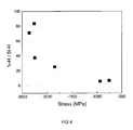
FIG 4 is a graph plotting the ratio of nitrogen bonded hydrogen (NHx) to silicon bonded hydrogen (SiH) content versus film stress. -
FIG 5 is a graph plotting NHx and SiH content versus film stress. - The present invention provides amino vinylsilane-based precursors as a way to increase the intrinsic compressive stress in plasma enhanced chemical vapor deposition (PECVD) silicon nitride (SiN) and silicon carbonitride (SiCN) thin films. The main feature of these amino vinylsilane precursors is at least one, preferably one or two, vinyl functional groups bonded to the central silicon atom. The precursors have the general formula:
[RR1N]xSiR3 y(R2)z
where x + y + z = 4, x = 1 - 3, y = 0 - 2, and z = 1 - 3. R and R1 can be hydrogen, C1 to C10 alkane, alkene, or C4 to C12 aromatic, or can be joined so that RR1N is a cyclic group, preferably a 5 or 6 membered cyclic group, such as a pyrrolidino or piperidino group; each R3 is hydrogen, C1 to C10 alkane, alkene, or C4 to C12 aromatic; and each R2 is a vinyl, allyl or other vinyl-containing functional group. The addition of a vinyl group to the aminosilane is found to increase the intrinsic compressive stress of SiN and SiCN films deposited using these precursors. - The amino vinylsilane precursors include, but are not limited to, Bis(isopropylamino)vinylmethylsilane (BIPAVNS), Bis(isopropylamino)divinylsilane (BIPADVS), Bis(isopropylamino)vinylsilane, Bis(isopropylamino)allylmethylsilane, Bis(isopropylamino)diallylsilane, Bis(isopropylamino)allylsilane, Bis(t-butylamino)vinylmethylsilane, Bis(t-butylaminoamino)divinylsilane, Bis(t-butylaminoamino)vinylsilane, Bis(t-butylaminoamino)allylmethylsilane, Bis(t-butylaminoamino)diallylsilane, Bis(t-butylaminoamino)allylsilane, Bis(diethylamino)vinylmethylsilane, Bis(diethylamino)divinylsilane, Bis(diethylamino)vinylsilane, Bis(diethylamino)allylmethylsilane, Bis(diethylamino)diallylsilane, Bis(diethylamino)allylsilane, Bis(dimethylamino)vinylmethylsilane, Bis(dimethylamino)divinylsilane, Bis(dimethylamino)vinylsilane, Bis(dimethylamino)allylmethylsilane, Bis(dimethylamino)diallylsilane, Bis(dimethylamino)allylsilane, Bis(methylethylamino)vinylmethylsilane, Bis(methyethylamino)divinylsilane, Bis(methyethylamino)vinylsilane, Bis(methyethylamino)allylmethylsilane, Bis(methyethylamino)diallylsilane, Bis(methyethylamino)allylsilane, Dipiperidinovinylmethylsilane, Dipiperidinodivinylsilane, Dipiperidinovinylsilane, Dipiperidinoallylmethylsilane, Dipiperidinodiallylsilane, Dipiperidinoallylsilane, Dipyrrolidinovinylmethylsilane, Dipyrrolidinodivinylsilane, Dipyrrolidinovinylsilane, Dipyrrolidinoallylmethylsilane, Dipyrrolidinodiallylsilane, Dipyrrolidinoallylsilane.
- The particular precursor used in tests is Bis(iso-propylamino)vinylmethylsilane (BIPAVMS). Another similar precursor is Bis(iso-propylamino)divinylsilane (BIPADVS).
- Stress engineering of PECVD silicon nitride films is currently being used to enhance the performance of cutting edge MOSFET technology. Device speed has been significantly increased through the application of highly stressed SiN films deposited on top of MOSFET gate structures. Compressive stress enhances pFET devices through increases of hole mobility, while tensile stress is beneficial for nFET devices through enhancing electron mobility. Stress is generated from differences in the thermal expansion between two materials in contact. PECVD silicon nitride films generally generate compressive stress. Presently, compressively stressed films are deposited using silane and ammonia with reported compressive stresses up to ∼ -3.5 GPa. Increasing compressive stress further is becoming particularly challenging. The industry is currently aiming for compressively stressed films of -4 GPa or higher.
- The goal of -4 GPa compressively stressed films may be realized through the use of the above described amino vinylsilane precursors. In the present invention, compressive stress of -0.7 to -4.5 GPa (-700 to -4500 MPa ) can be obtained. Up to now, most of the increases in stress generation have been through processing techniques, such as plasma surface treatment, multilayer deposition, dual frequency plasma and other similar methods. This invention is the first to specifically use a unique type of silicon-containing precursor to increase film stress.
- Standard deposition methods have a limit to the amount of stress they can generate. Current targets for stress are 1.5GPa for tensile stress and -4 GPa for compressive stress.
- It has been observed that higher hydrogen incorporation into SiN films leads to higher compressive stress. We propose that PECVD SiN films deposited using amino vinylsilanes such as BIPADVS and BIPAVMS can generate highly compressive stress due to overall hydrogen incorporation and, moreover, through the type of hydrogen incorporation, i.e. nitrogen bonded hydrogen vs silicon bonded hydrogen. We have shown for both bis(tertiary-butylamino)silane (BTBAS) and BIPAVMS a strong correlation between N-H to Si-H ratio and compressive stress, with high N-H to Si-H ratio leading to higher compressive stress. Films deposited using a mixture of an aminosilane and ammonia naturally lead to films containing high N-H to Si-H content through transamination reactions
- Furthermore, aminosilanes containing vinyl functional groups, such as BIPADVS and BIPAVMS, have been found to increase compressive stress further. Vinyl groups play important roles in creating film stress. Under plasma conditions, carbon-carbon double bonds may form cross-linking points, which increase the density of film by holding atoms closer. Si-H bonds of the precursor react with carbon-carbon double bonds with hydrosilylation reaction, forming ethylene bridges between silicon atoms. Ethylene bridges hold the silicon atoms close, and are consequently replaced by ammonia, and that process helps the formation of Si-N-Si structure.

- The present invention is directed to overcome limits of intrinsic stress generation through the use of this special class of aminosilane precursors, namely amino vinylsilanes, to deposit highly stressed silicon nitride (SiN) films or silicon carbonitride (SiCN) films using PEVCD. The addition of a vinyl group to the aminosilane is found to increase the intrinsic compressive stress of SiN and SiCN films deposited using these precursors.
- To deposit compressively stressed silicon nitride or silicon carbonitride films, the amino vinylsilane is, preferably, reacted with a nitrogen-containing gas in a PECVD chamber at wafer temperatures of 500°C or less. The nitrogen containing gas can be ammonia, nitrogen, or a combination thereof. Additionally, a diluent gas such as, but not limited to, He, Ar, Ne, Xe, or hydrogen can be introduced to modify the film properties. For example, Bis(iso-propylamino)vinylmethylsilane (BIPAVMS) (
FIG 1 A) or Bis(iso-propylamino)divinylsilane (BIPADVS) (FIG 1 B) and ammonia can be introduced into a PECVD chamber and allowed to react, resulting in the deposition of a compressively stressed SiN thin film. A suitable BIPAVMS, or other amino vinylsilane, flow rate may range from 50 to 1000 mg/min. A suitable ammonia and/or nitrogen (or other nitrogen containing reactant) flow rate may range from 500 to 10,000 sccm, and suitable diluent gas flow rates may range from 50 to 50,000 sccm. - Depositions conditions for Runs A-F and the corresponding film stress obtained in Table 1, below, are as follows. Deposition temperature was 400 C. In these examples, properties were obtained from sample films that were deposited onto medium resistivity (8-12 Ωcm) single crystal silicon wafer substrates. All depositions were performed on an Applied Materials Precision 5000 system in a 200 mm DXZ chamber fitted with an
Advanced Energy 2000 RF generator. The plasma is single frequency of 13.56 MHz. - In the Table 1 examples, thickness and optical properties, such as refractive index of the dielectric films, were measured on an SCI Filmtek Reflectometer. The refractive index is measured using 632 nm wavelength light. Fourier Infrared Spectroscopy (FTIR) data was collected on the wafers using a Thermo Nicolet 750 system in a nitrogen purged cell. Background spectra were collected on similar medium resistivity wafers to eliminate CO2 and water from the spectra. Data was obtained in the range of from 4000 to 400 cm-1 by collecting 32 scans with a resolution of 4 cm-1. The OMNIC software package was used to process the data. Film stress measurements were made using a laser beam scattering tool (Toho Technology Corp., Model: FLX2320S).
Table 1 Film BIPAVMS flow NH3 P Power Stress (mg/min) (sccm) (Torr) (W) (MPa) A 250 2500 2.5 (330 Pa) 400 -1849 B 250 1250 2.5 (330 Pa) 400 -934 C 250 2500 4 (530 Pa) 400 -757 D 250 2500 2.5 (330 Pa) 600 -2249 E 125 2500 2.5 (330 Pa) 400 -2357 F 125 2500 2.5 (330 Pa) 600 -2260 - Film stress data of silicon nitride films deposited at 400°C using Bis(iso-propylamino)vinylmethylsilane and ammonia is shown in
FIG 2 . The films were deposited under various process conditions, with precursor and gas flow rate, pressure, and RF power all being varied. The films were single layer, with thicknesses ranging from 100 to 350 nm. The plasma was generated using a single frequency of 13.56 MHz. The compressive stress of these films ranged from -700 to -2400 mega pascales (MPa). These films produced ∼1.5 to 1.8x higher compressive stress than BTBAS under comparable process conditions. -
FIG 3 shows the FTIR spectra of films fromFIG 2 with the lowest (Film C) and highest (Film E) compressive stress. Both films exhibit NHx stretching and bending modes of similar intensity. However, there is a distinct difference in the SiH peak at ∼2190 cm-1, thus suggesting the main difference is in whether hydrogen is bonded to nitrogen or silicon. -
FIG 4 depicts the correlation between the ratio of NHx to SiH with stress. As can be seen from this figure, stress increases with higher NHx to SiH ratio. Preferably, the deposited thin film has a N-H to Si-H ratio of 25 to 85, most preferably 70. -
FIG 5 depicts the correlation of nitrogen bonded hydrogen (NHx) to stress and silicon bonded hydrogen to stress. This data indicates that reduction of SiH groups in addition to high levels of NHx moiety is important in generating high levels of compressive stress. Hydrogen contents derived from NHx moieties increase compressive stress in the range of 2.9 to 3.5 H content/cm3 x 1022, preferably 3.3 to 3.6 H content/cm3 x 1022 - Experimental data indicate that films possessing higher stress values were found not to contain carbon. It is inferred that the carbon is etched away by the ammonia, which is in high excess compared to the precursor. In higher stress SiN films, more Si-H bonds are removed by the hydrosilylation of vinyl group, and replaced with N-H by the removal of ethylene bridge by ammonia.
- Under process condition A listed in Table 1, the stress of films using non-vinyl precursor (such as BTBAS) is lower than that for (BIPAVMS)
Table 2 Precursor Thickness
(nm)Dep. Rate
(nm/min)RI Stress
(MPa)BIPAVMS 208 13.9 1.97 -1849 BTBAS 136 13.6 1.97 -1034 - Under process condition A listed in Table 1, but an alternative tool and showerhead configuration, the stress of films deposited increases as the number of vinyl groups increases in precursor.
Table 3 Precursor Vinyl groups Stress (MPa) BIPAVMS 1 -1200 BIPADVS 2 -1705
Claims (15)
- A method of depositing an intrinsically compressively stressed silicon nitride or silicon carbonitride thin film, comprising depositing the film from an amino vinylsilane-based precursor using plasma enhanced chemical vapor deposition.
- The method of Claim 1 wherein the amino vinylsilane-based precursor is selected from the formula:
[RR1N]xSiR3 y(R2)z
where x + y + z = 4, x = 1 to 3, y = 0 to 2, and z = 1 to 3; R and R1 are selected from hydrogen, C1 to C10 alkane, C1 to C10 alkene, and C4 to C12 aromatic, or can be joined so that RR1N is a cyclic group; each R3 is a hydrogen, C1 to C10 alkane, C1 to C10 alkene, or C4 to C12 aromatic; and each R2 is a vinyl, allyl or vinyl-containing functional group. - The method of Claim 2 wherein the amino vinylsilane based precursor is selected from Bis(iso-propylamino)vinylmethylsilane, Bis(iso-propylamino)divinylsilane and mixtures thereof.
- The method of any preceding claim wherein the flow rate of the amino vinylsilane-based precursor is 50 to 1000 mg/min.
- The method of any preceding claim wherein a nitrogen containing reactant is reacted with the amino vinylsilane-based precursor.
- The method of Claim 5 wherein the nitrogen containing reactant is selected from ammonia, nitrogen and mixtures thereof.
- The method of Claim 5 or 6 wherein the flow rate of the nitrogen containing reactant is 500 to 10,000 mg/min.
- The method of any preceding claim wherein the deposition is conducted in the presence of a diluent gas selected from helium, argon, neon, xenon and mixtures thereof.
- The method of Claim 8 wherein the flow rate of the diluent gas is 50 to 50,000 mg/min.
- The method of any preceding claim wherein the deposition is conducted at an elevated temperature at or below 500°C.
- The method of any preceding claim wherein the deposited thin film has a N-H to Si-H ratio of 25 to 85.
- The method of any preceding claim wherein the deposited thin film has a N-H derived H content/cm3 x 1022 in the range of 3.3 to 3.6.
- The method of any preceding claim wherein the deposited thin film has a compressive stress of -700 to -2400 MPa.
- The method of any one of Claims 1 to 12 wherein the deposited thin film has a compressive stress of -700 to -4500 MPa.
- The method of any one of Claims 1 to 12 wherein the compressively stressed films have a compressive stress of -4 GPa or higher.
Priority Applications (1)
| Application Number | Priority Date | Filing Date | Title |
|---|---|---|---|
| EP12159248A EP2465861A1 (en) | 2008-11-12 | 2009-11-12 | Amino vinylsilane precursors for compressively stressed SiN films |
Applications Claiming Priority (2)
| Application Number | Priority Date | Filing Date | Title |
|---|---|---|---|
| US11362408P | 2008-11-12 | 2008-11-12 | |
| US12/609,542 US8580993B2 (en) | 2008-11-12 | 2009-10-30 | Amino vinylsilane precursors for stressed SiN films |
Related Child Applications (1)
| Application Number | Title | Priority Date | Filing Date |
|---|---|---|---|
| EP12159248.9 Division-Into | 2012-03-13 |
Publications (2)
| Publication Number | Publication Date |
|---|---|
| EP2192207A1 true EP2192207A1 (en) | 2010-06-02 |
| EP2192207B1 EP2192207B1 (en) | 2012-06-20 |
Family
ID=41509788
Family Applications (2)
| Application Number | Title | Priority Date | Filing Date |
|---|---|---|---|
| EP12159248A Withdrawn EP2465861A1 (en) | 2008-11-12 | 2009-11-12 | Amino vinylsilane precursors for compressively stressed SiN films |
| EP09175806A Not-in-force EP2192207B1 (en) | 2008-11-12 | 2009-11-12 | Method using amino vinylsilane precursors for the deposition of intrinsically compressively stressed SiN films |
Family Applications Before (1)
| Application Number | Title | Priority Date | Filing Date |
|---|---|---|---|
| EP12159248A Withdrawn EP2465861A1 (en) | 2008-11-12 | 2009-11-12 | Amino vinylsilane precursors for compressively stressed SiN films |
Country Status (6)
| Country | Link |
|---|---|
| US (2) | US8580993B2 (en) |
| EP (2) | EP2465861A1 (en) |
| JP (2) | JP5175261B2 (en) |
| KR (2) | KR101396139B1 (en) |
| CN (2) | CN101899651B (en) |
| TW (2) | TWI437117B (en) |
Cited By (2)
| Publication number | Priority date | Publication date | Assignee | Title |
|---|---|---|---|---|
| EP2251899A1 (en) * | 2009-05-13 | 2010-11-17 | Air Products and Chemicals, Inc. | Dielectric barrier deposition using nitrogen containing precursor |
| EP3882976A1 (en) * | 2020-03-19 | 2021-09-22 | Samsung Display Co., Ltd. | Display device |
Families Citing this family (23)
| Publication number | Priority date | Publication date | Assignee | Title |
|---|---|---|---|---|
| US8580993B2 (en) | 2008-11-12 | 2013-11-12 | Air Products And Chemicals, Inc. | Amino vinylsilane precursors for stressed SiN films |
| US9892917B2 (en) | 2010-04-15 | 2018-02-13 | Lam Research Corporation | Plasma assisted atomic layer deposition of multi-layer films for patterning applications |
| US8637411B2 (en) | 2010-04-15 | 2014-01-28 | Novellus Systems, Inc. | Plasma activated conformal dielectric film deposition |
| US9257274B2 (en) | 2010-04-15 | 2016-02-09 | Lam Research Corporation | Gapfill of variable aspect ratio features with a composite PEALD and PECVD method |
| US9373500B2 (en) | 2014-02-21 | 2016-06-21 | Lam Research Corporation | Plasma assisted atomic layer deposition titanium oxide for conformal encapsulation and gapfill applications |
| US9997357B2 (en) | 2010-04-15 | 2018-06-12 | Lam Research Corporation | Capped ALD films for doping fin-shaped channel regions of 3-D IC transistors |
| US8460753B2 (en) * | 2010-12-09 | 2013-06-11 | Air Products And Chemicals, Inc. | Methods for depositing silicon dioxide or silicon oxide films using aminovinylsilanes |
| US8647993B2 (en) * | 2011-04-11 | 2014-02-11 | Novellus Systems, Inc. | Methods for UV-assisted conformal film deposition |
| EP2714960B1 (en) | 2011-06-03 | 2018-02-28 | Versum Materials US, LLC | Compositions and processes for depositing carbon-doped silicon-containing films |
| SG2013083654A (en) | 2012-11-08 | 2014-06-27 | Novellus Systems Inc | Methods for depositing films on sensitive substrates |
| US9564312B2 (en) | 2014-11-24 | 2017-02-07 | Lam Research Corporation | Selective inhibition in atomic layer deposition of silicon-containing films |
| US10566187B2 (en) | 2015-03-20 | 2020-02-18 | Lam Research Corporation | Ultrathin atomic layer deposition film accuracy thickness control |
| KR20170019668A (en) * | 2015-08-12 | 2017-02-22 | (주)디엔에프 | The manufacturing method of the silicon nitride film by using plasma enhanced atomic layer deposition |
| US9773643B1 (en) | 2016-06-30 | 2017-09-26 | Lam Research Corporation | Apparatus and method for deposition and etch in gap fill |
| US10062563B2 (en) | 2016-07-01 | 2018-08-28 | Lam Research Corporation | Selective atomic layer deposition with post-dose treatment |
| WO2018016871A1 (en) * | 2016-07-22 | 2018-01-25 | (주)디엔에프 | Method for manufacturing silicon nitride thin film using plasma atomic layer deposition |
| US10037884B2 (en) | 2016-08-31 | 2018-07-31 | Lam Research Corporation | Selective atomic layer deposition for gapfill using sacrificial underlayer |
| US10269559B2 (en) | 2017-09-13 | 2019-04-23 | Lam Research Corporation | Dielectric gapfill of high aspect ratio features utilizing a sacrificial etch cap layer |
| SG11202111962QA (en) | 2019-05-01 | 2021-11-29 | Lam Res Corp | Modulated atomic layer deposition |
| JP2022534793A (en) | 2019-06-07 | 2022-08-03 | ラム リサーチ コーポレーション | In situ control of film properties during atomic layer deposition |
| CN116113725B (en) | 2020-07-24 | 2025-10-31 | 弗萨姆材料美国有限责任公司 | Composition for germanium seed layer and method of using the same |
| WO2023102376A1 (en) * | 2021-12-01 | 2023-06-08 | Lam Research Corporation | Deposition of high compressive stress thermally stable nitride film |
| CN114447435A (en) * | 2022-01-21 | 2022-05-06 | 恒实科技发展(南京)有限公司 | Non-aqueous electrolyte for lithium secondary battery and preparation method and application thereof |
Citations (8)
| Publication number | Priority date | Publication date | Assignee | Title |
|---|---|---|---|---|
| EP1441042A1 (en) | 2003-01-23 | 2004-07-28 | Air Products And Chemicals, Inc. | Precursors for depositing silicon containing films and processes thereof |
| US20050080285A1 (en) * | 2003-10-10 | 2005-04-14 | Ziyun Wang | Monosilane or disilane derivatives and method for low temperature deposition of silicon-containing films using the same |
| US20060014399A1 (en) * | 2004-07-14 | 2006-01-19 | Tokyo Electron Limited | Low-temperature plasma-enhanced chemical vapor deposition of silicon-nitrogen-containing films |
| EP1630249A2 (en) | 2004-08-30 | 2006-03-01 | Air Products And Chemicals, Inc. | Process for chemical vapor deposition of silicon nitride. |
| US20060258173A1 (en) | 2005-05-16 | 2006-11-16 | Manchao Xiao | Precursors for CVD silicon carbo-nitride films |
| WO2006127462A2 (en) | 2005-05-26 | 2006-11-30 | Applied Materials, Inc. | Method to increase the compressive stress of pecvd silicon nitride films |
| EP1932941A1 (en) | 2006-12-13 | 2008-06-18 | Air Products and Chemicals, Inc. | Thermal etch process for cleaning CVD chambers |
| US20080146007A1 (en) | 2006-12-14 | 2008-06-19 | Mihaela Balseanu | Method to increase the compressive stress of pecvd dielectric films |
Family Cites Families (13)
| Publication number | Priority date | Publication date | Assignee | Title |
|---|---|---|---|---|
| JP2854787B2 (en) * | 1993-08-31 | 1999-02-03 | 信越化学工業株式会社 | Method for producing silicone rubber composition |
| JP3430097B2 (en) | 1999-12-22 | 2003-07-28 | 日本電気株式会社 | Method of manufacturing thin film transistor array substrate |
| JP2002246381A (en) * | 2001-02-15 | 2002-08-30 | Anelva Corp | CVD method |
| JP2004223769A (en) * | 2003-01-20 | 2004-08-12 | Dainippon Printing Co Ltd | Transparent laminated film, antireflection film, polarizing plate using the same, and liquid crystal display |
| JP2005310861A (en) | 2004-04-19 | 2005-11-04 | Mitsui Chemicals Inc | Sintered silicon nitride film forming method |
| JP2006120992A (en) | 2004-10-25 | 2006-05-11 | C Bui Res:Kk | Silicon nitride film manufacturing method and manufacturing apparatus thereof |
| US20060182885A1 (en) * | 2005-02-14 | 2006-08-17 | Xinjian Lei | Preparation of metal silicon nitride films via cyclic deposition |
| JP2006294485A (en) | 2005-04-13 | 2006-10-26 | Konica Minolta Holdings Inc | ORGANIC ELECTROLUMINESCENCE ELEMENT, ITS MANUFACTURING METHOD, AND DISPLAY DEVICE |
| EP1908767B1 (en) * | 2005-05-31 | 2012-06-13 | Toho Titanium Co., Ltd. | Aminosilane compounds, catalyst components and catalysts for olefin polymerization, and process for production of olefin polymers with the same |
| JP2007092166A (en) * | 2005-09-02 | 2007-04-12 | Japan Advanced Institute Of Science & Technology Hokuriku | Thin film deposition apparatus, thin film deposition method, and compound thin film |
| EP2123445A4 (en) | 2007-02-05 | 2012-04-11 | Konica Minolta Holdings Inc | Transparent gas barrier film and method for producing the same |
| JP5391557B2 (en) * | 2007-02-28 | 2014-01-15 | 住友化学株式会社 | Conjugated diene polymer, process for producing conjugated diene polymer, and conjugated diene polymer composition |
| US8580993B2 (en) * | 2008-11-12 | 2013-11-12 | Air Products And Chemicals, Inc. | Amino vinylsilane precursors for stressed SiN films |
-
2009
- 2009-10-30 US US12/609,542 patent/US8580993B2/en not_active Expired - Fee Related
- 2009-11-09 TW TW100140431A patent/TWI437117B/en not_active IP Right Cessation
- 2009-11-09 TW TW098137987A patent/TWI412622B/en not_active IP Right Cessation
- 2009-11-11 KR KR1020090108666A patent/KR101396139B1/en not_active Expired - Fee Related
- 2009-11-12 JP JP2009259203A patent/JP5175261B2/en not_active Expired - Fee Related
- 2009-11-12 EP EP12159248A patent/EP2465861A1/en not_active Withdrawn
- 2009-11-12 EP EP09175806A patent/EP2192207B1/en not_active Not-in-force
- 2009-11-12 CN CN2009102468369A patent/CN101899651B/en not_active Expired - Fee Related
- 2009-11-12 CN CN201110404812.9A patent/CN102491990B/en not_active Expired - Fee Related
-
2012
- 2012-09-27 JP JP2012214658A patent/JP5508496B2/en active Active
- 2012-12-28 KR KR1020120156542A patent/KR101553863B1/en not_active Expired - Fee Related
-
2013
- 2013-11-04 US US14/070,957 patent/US20140065844A1/en not_active Abandoned
Patent Citations (13)
| Publication number | Priority date | Publication date | Assignee | Title |
|---|---|---|---|---|
| US7288145B2 (en) | 2003-01-23 | 2007-10-30 | Air Products And Chemicals, Inc. | Precursors for depositing silicon containing films |
| US7122222B2 (en) | 2003-01-23 | 2006-10-17 | Air Products And Chemicals, Inc. | Precursors for depositing silicon containing films and processes thereof |
| EP1441042A1 (en) | 2003-01-23 | 2004-07-28 | Air Products And Chemicals, Inc. | Precursors for depositing silicon containing films and processes thereof |
| US20050080285A1 (en) * | 2003-10-10 | 2005-04-14 | Ziyun Wang | Monosilane or disilane derivatives and method for low temperature deposition of silicon-containing films using the same |
| US20060014399A1 (en) * | 2004-07-14 | 2006-01-19 | Tokyo Electron Limited | Low-temperature plasma-enhanced chemical vapor deposition of silicon-nitrogen-containing films |
| EP1630249A2 (en) | 2004-08-30 | 2006-03-01 | Air Products And Chemicals, Inc. | Process for chemical vapor deposition of silicon nitride. |
| US20060045986A1 (en) | 2004-08-30 | 2006-03-02 | Hochberg Arthur K | Silicon nitride from aminosilane using PECVD |
| US20060258173A1 (en) | 2005-05-16 | 2006-11-16 | Manchao Xiao | Precursors for CVD silicon carbo-nitride films |
| EP1724373A1 (en) | 2005-05-16 | 2006-11-22 | Air Products and Chemicals, Inc. | Precursors for cvd silicon carbo-nitride films |
| WO2006127462A2 (en) | 2005-05-26 | 2006-11-30 | Applied Materials, Inc. | Method to increase the compressive stress of pecvd silicon nitride films |
| US20060269692A1 (en) | 2005-05-26 | 2006-11-30 | Applied Materials, Inc. A Delaware Corporation | Method to increase the compressive stress of PECVD silicon nitride films |
| EP1932941A1 (en) | 2006-12-13 | 2008-06-18 | Air Products and Chemicals, Inc. | Thermal etch process for cleaning CVD chambers |
| US20080146007A1 (en) | 2006-12-14 | 2008-06-19 | Mihaela Balseanu | Method to increase the compressive stress of pecvd dielectric films |
Non-Patent Citations (1)
| Title |
|---|
| M. BELYANSKY ET AL.: "Methods of producing plasma enhanced chemical vapor deposition silicon nitride thin films with high compressive and tensile stress", J. VAC. SCI. TECHNOL. A, vol. 26, no. 3, 2008, pages 517 |
Cited By (3)
| Publication number | Priority date | Publication date | Assignee | Title |
|---|---|---|---|---|
| EP2251899A1 (en) * | 2009-05-13 | 2010-11-17 | Air Products and Chemicals, Inc. | Dielectric barrier deposition using nitrogen containing precursor |
| US8889235B2 (en) | 2009-05-13 | 2014-11-18 | Air Products And Chemicals, Inc. | Dielectric barrier deposition using nitrogen containing precursor |
| EP3882976A1 (en) * | 2020-03-19 | 2021-09-22 | Samsung Display Co., Ltd. | Display device |
Also Published As
| Publication number | Publication date |
|---|---|
| JP2010118664A (en) | 2010-05-27 |
| US20100120262A1 (en) | 2010-05-13 |
| KR20100053471A (en) | 2010-05-20 |
| TW201211303A (en) | 2012-03-16 |
| CN101899651B (en) | 2012-12-26 |
| JP5175261B2 (en) | 2013-04-03 |
| TWI412622B (en) | 2013-10-21 |
| EP2192207B1 (en) | 2012-06-20 |
| KR20130016171A (en) | 2013-02-14 |
| US20140065844A1 (en) | 2014-03-06 |
| KR101553863B1 (en) | 2015-09-17 |
| TWI437117B (en) | 2014-05-11 |
| TW201018741A (en) | 2010-05-16 |
| JP5508496B2 (en) | 2014-05-28 |
| US8580993B2 (en) | 2013-11-12 |
| EP2465861A1 (en) | 2012-06-20 |
| CN101899651A (en) | 2010-12-01 |
| CN102491990A (en) | 2012-06-13 |
| CN102491990B (en) | 2015-12-09 |
| KR101396139B1 (en) | 2014-05-19 |
| JP2013016859A (en) | 2013-01-24 |
Similar Documents
| Publication | Publication Date | Title |
|---|---|---|
| EP2192207B1 (en) | Method using amino vinylsilane precursors for the deposition of intrinsically compressively stressed SiN films | |
| US6716770B2 (en) | Low dielectric constant material and method of processing by CVD | |
| KR100642618B1 (en) | Porous low dielectric constant compositions and methods for making and using same | |
| KR101144535B1 (en) | Dielectric barrier deposition using nitrogen containing precursor | |
| US6632478B2 (en) | Process for forming a low dielectric constant carbon-containing film | |
| US20030194496A1 (en) | Methods for depositing dielectric material | |
| CN100437933C (en) | Methods for Improving Interlayer Adhesion | |
| EP2692897A1 (en) | Non-oxygen containing silicon-based films and methods of forming the same | |
| US20030139035A1 (en) | Low dielectric (low k) barrier films with oxygen doping by plasma-enhanced chemical vapor deposition (pecvd) | |
| KR20070007937A (en) | Improved adhesion of low k dielectric materials to conductive materials | |
| US7326444B1 (en) | Methods for improving integration performance of low stress CDO films | |
| CN101205607A (en) | Method for Increasing Compressive Stress of Plasma Enhanced Chemical Vapor Deposition Dielectric Films | |
| US7074489B2 (en) | Low dielectric constant material and method of processing by CVD | |
| EP2302667A1 (en) | Insulating film for semiconductor device, process and apparatus for producing insulating film for semiconductor device, semiconductor device, and process for producing the semiconductor device | |
| KR20240009497A (en) | Novel precursor for deposition of films with high elastic modulus | |
| JP5731841B2 (en) | Method for forming silicon nitride film | |
| TW202217051A (en) | Alkoxydisiloxanes and dense organosilica films made therefrom | |
| EP4110969A1 (en) | New precursors for depositing films with high elastic modulus | |
| Nowling | High-pressure plasma deposition of silicon nitride and silicon dioxide |
Legal Events
| Date | Code | Title | Description |
|---|---|---|---|
| PUAI | Public reference made under article 153(3) epc to a published international application that has entered the european phase |
Free format text: ORIGINAL CODE: 0009012 |
|
| AK | Designated contracting states |
Kind code of ref document: A1 Designated state(s): AT BE BG CH CY CZ DE DK EE ES FI FR GB GR HR HU IE IS IT LI LT LU LV MC MK MT NL NO PL PT RO SE SI SK SM TR |
|
| 17P | Request for examination filed |
Effective date: 20100727 |
|
| 17Q | First examination report despatched |
Effective date: 20100818 |
|
| RIC1 | Information provided on ipc code assigned before grant |
Ipc: C23C 16/34 20060101AFI20110810BHEP Ipc: C23C 16/36 20060101ALI20110810BHEP |
|
| GRAP | Despatch of communication of intention to grant a patent |
Free format text: ORIGINAL CODE: EPIDOSNIGR1 |
|
| GRAJ | Information related to disapproval of communication of intention to grant by the applicant or resumption of examination proceedings by the epo deleted |
Free format text: ORIGINAL CODE: EPIDOSDIGR1 |
|
| GRAP | Despatch of communication of intention to grant a patent |
Free format text: ORIGINAL CODE: EPIDOSNIGR1 |
|
| RTI1 | Title (correction) |
Free format text: METHOD USING AMINO VINYLSILANE PRECURSORS FOR THE DEPOSITION OF INTRINSICALLY COMPRESSIVELY STRESSED SIN FILMS |
|
| GRAS | Grant fee paid |
Free format text: ORIGINAL CODE: EPIDOSNIGR3 |
|
| GRAA | (expected) grant |
Free format text: ORIGINAL CODE: 0009210 |
|
| AK | Designated contracting states |
Kind code of ref document: B1 Designated state(s): AT BE BG CH CY CZ DE DK EE ES FI FR GB GR HR HU IE IS IT LI LT LU LV MC MK MT NL NO PL PT RO SE SI SK SM TR |
|
| REG | Reference to a national code |
Ref country code: GB Ref legal event code: FG4D |
|
| REG | Reference to a national code |
Ref country code: CH Ref legal event code: EP |
|
| REG | Reference to a national code |
Ref country code: AT Ref legal event code: REF Ref document number: 563128 Country of ref document: AT Kind code of ref document: T Effective date: 20120715 |
|
| REG | Reference to a national code |
Ref country code: IE Ref legal event code: FG4D |
|
| REG | Reference to a national code |
Ref country code: DE Ref legal event code: R096 Ref document number: 602009007664 Country of ref document: DE Effective date: 20120823 |
|
| PG25 | Lapsed in a contracting state [announced via postgrant information from national office to epo] |
Ref country code: SE Free format text: LAPSE BECAUSE OF FAILURE TO SUBMIT A TRANSLATION OF THE DESCRIPTION OR TO PAY THE FEE WITHIN THE PRESCRIBED TIME-LIMIT Effective date: 20120620 Ref country code: NO Free format text: LAPSE BECAUSE OF FAILURE TO SUBMIT A TRANSLATION OF THE DESCRIPTION OR TO PAY THE FEE WITHIN THE PRESCRIBED TIME-LIMIT Effective date: 20120920 Ref country code: LT Free format text: LAPSE BECAUSE OF FAILURE TO SUBMIT A TRANSLATION OF THE DESCRIPTION OR TO PAY THE FEE WITHIN THE PRESCRIBED TIME-LIMIT Effective date: 20120620 Ref country code: FI Free format text: LAPSE BECAUSE OF FAILURE TO SUBMIT A TRANSLATION OF THE DESCRIPTION OR TO PAY THE FEE WITHIN THE PRESCRIBED TIME-LIMIT Effective date: 20120620 |
|
| REG | Reference to a national code |
Ref country code: NL Ref legal event code: VDEP Effective date: 20120620 |
|
| REG | Reference to a national code |
Ref country code: AT Ref legal event code: MK05 Ref document number: 563128 Country of ref document: AT Kind code of ref document: T Effective date: 20120620 |
|
| REG | Reference to a national code |
Ref country code: LT Ref legal event code: MG4D Effective date: 20120620 |
|
| PG25 | Lapsed in a contracting state [announced via postgrant information from national office to epo] |
Ref country code: GR Free format text: LAPSE BECAUSE OF FAILURE TO SUBMIT A TRANSLATION OF THE DESCRIPTION OR TO PAY THE FEE WITHIN THE PRESCRIBED TIME-LIMIT Effective date: 20120921 Ref country code: LV Free format text: LAPSE BECAUSE OF FAILURE TO SUBMIT A TRANSLATION OF THE DESCRIPTION OR TO PAY THE FEE WITHIN THE PRESCRIBED TIME-LIMIT Effective date: 20120620 Ref country code: HR Free format text: LAPSE BECAUSE OF FAILURE TO SUBMIT A TRANSLATION OF THE DESCRIPTION OR TO PAY THE FEE WITHIN THE PRESCRIBED TIME-LIMIT Effective date: 20120620 Ref country code: SI Free format text: LAPSE BECAUSE OF FAILURE TO SUBMIT A TRANSLATION OF THE DESCRIPTION OR TO PAY THE FEE WITHIN THE PRESCRIBED TIME-LIMIT Effective date: 20120620 |
|
| PG25 | Lapsed in a contracting state [announced via postgrant information from national office to epo] |
Ref country code: IS Free format text: LAPSE BECAUSE OF FAILURE TO SUBMIT A TRANSLATION OF THE DESCRIPTION OR TO PAY THE FEE WITHIN THE PRESCRIBED TIME-LIMIT Effective date: 20121020 Ref country code: CZ Free format text: LAPSE BECAUSE OF FAILURE TO SUBMIT A TRANSLATION OF THE DESCRIPTION OR TO PAY THE FEE WITHIN THE PRESCRIBED TIME-LIMIT Effective date: 20120620 Ref country code: AT Free format text: LAPSE BECAUSE OF FAILURE TO SUBMIT A TRANSLATION OF THE DESCRIPTION OR TO PAY THE FEE WITHIN THE PRESCRIBED TIME-LIMIT Effective date: 20120620 Ref country code: EE Free format text: LAPSE BECAUSE OF FAILURE TO SUBMIT A TRANSLATION OF THE DESCRIPTION OR TO PAY THE FEE WITHIN THE PRESCRIBED TIME-LIMIT Effective date: 20120620 Ref country code: BE Free format text: LAPSE BECAUSE OF FAILURE TO SUBMIT A TRANSLATION OF THE DESCRIPTION OR TO PAY THE FEE WITHIN THE PRESCRIBED TIME-LIMIT Effective date: 20120620 Ref country code: RO Free format text: LAPSE BECAUSE OF FAILURE TO SUBMIT A TRANSLATION OF THE DESCRIPTION OR TO PAY THE FEE WITHIN THE PRESCRIBED TIME-LIMIT Effective date: 20120620 Ref country code: SK Free format text: LAPSE BECAUSE OF FAILURE TO SUBMIT A TRANSLATION OF THE DESCRIPTION OR TO PAY THE FEE WITHIN THE PRESCRIBED TIME-LIMIT Effective date: 20120620 Ref country code: CY Free format text: LAPSE BECAUSE OF FAILURE TO SUBMIT A TRANSLATION OF THE DESCRIPTION OR TO PAY THE FEE WITHIN THE PRESCRIBED TIME-LIMIT Effective date: 20120620 |
|
| PG25 | Lapsed in a contracting state [announced via postgrant information from national office to epo] |
Ref country code: PT Free format text: LAPSE BECAUSE OF FAILURE TO SUBMIT A TRANSLATION OF THE DESCRIPTION OR TO PAY THE FEE WITHIN THE PRESCRIBED TIME-LIMIT Effective date: 20121022 Ref country code: PL Free format text: LAPSE BECAUSE OF FAILURE TO SUBMIT A TRANSLATION OF THE DESCRIPTION OR TO PAY THE FEE WITHIN THE PRESCRIBED TIME-LIMIT Effective date: 20120620 Ref country code: IT Free format text: LAPSE BECAUSE OF FAILURE TO SUBMIT A TRANSLATION OF THE DESCRIPTION OR TO PAY THE FEE WITHIN THE PRESCRIBED TIME-LIMIT Effective date: 20120620 |
|
| PG25 | Lapsed in a contracting state [announced via postgrant information from national office to epo] |
Ref country code: NL Free format text: LAPSE BECAUSE OF FAILURE TO SUBMIT A TRANSLATION OF THE DESCRIPTION OR TO PAY THE FEE WITHIN THE PRESCRIBED TIME-LIMIT Effective date: 20120620 |
|
| PLBE | No opposition filed within time limit |
Free format text: ORIGINAL CODE: 0009261 |
|
| STAA | Information on the status of an ep patent application or granted ep patent |
Free format text: STATUS: NO OPPOSITION FILED WITHIN TIME LIMIT |
|
| PG25 | Lapsed in a contracting state [announced via postgrant information from national office to epo] |
Ref country code: DK Free format text: LAPSE BECAUSE OF FAILURE TO SUBMIT A TRANSLATION OF THE DESCRIPTION OR TO PAY THE FEE WITHIN THE PRESCRIBED TIME-LIMIT Effective date: 20120620 Ref country code: ES Free format text: LAPSE BECAUSE OF FAILURE TO SUBMIT A TRANSLATION OF THE DESCRIPTION OR TO PAY THE FEE WITHIN THE PRESCRIBED TIME-LIMIT Effective date: 20121001 |
|
| 26N | No opposition filed |
Effective date: 20130321 |
|
| REG | Reference to a national code |
Ref country code: DE Ref legal event code: R097 Ref document number: 602009007664 Country of ref document: DE Effective date: 20130321 |
|
| PG25 | Lapsed in a contracting state [announced via postgrant information from national office to epo] |
Ref country code: BG Free format text: LAPSE BECAUSE OF FAILURE TO SUBMIT A TRANSLATION OF THE DESCRIPTION OR TO PAY THE FEE WITHIN THE PRESCRIBED TIME-LIMIT Effective date: 20120920 |
|
| REG | Reference to a national code |
Ref country code: IE Ref legal event code: MM4A |
|
| PG25 | Lapsed in a contracting state [announced via postgrant information from national office to epo] |
Ref country code: IE Free format text: LAPSE BECAUSE OF NON-PAYMENT OF DUE FEES Effective date: 20121112 |
|
| PG25 | Lapsed in a contracting state [announced via postgrant information from national office to epo] |
Ref country code: MT Free format text: LAPSE BECAUSE OF FAILURE TO SUBMIT A TRANSLATION OF THE DESCRIPTION OR TO PAY THE FEE WITHIN THE PRESCRIBED TIME-LIMIT Effective date: 20120620 |
|
| PG25 | Lapsed in a contracting state [announced via postgrant information from national office to epo] |
Ref country code: MC Free format text: LAPSE BECAUSE OF NON-PAYMENT OF DUE FEES Effective date: 20121130 Ref country code: TR Free format text: LAPSE BECAUSE OF FAILURE TO SUBMIT A TRANSLATION OF THE DESCRIPTION OR TO PAY THE FEE WITHIN THE PRESCRIBED TIME-LIMIT Effective date: 20120620 |
|
| PG25 | Lapsed in a contracting state [announced via postgrant information from national office to epo] |
Ref country code: LU Free format text: LAPSE BECAUSE OF NON-PAYMENT OF DUE FEES Effective date: 20121112 Ref country code: SM Free format text: LAPSE BECAUSE OF FAILURE TO SUBMIT A TRANSLATION OF THE DESCRIPTION OR TO PAY THE FEE WITHIN THE PRESCRIBED TIME-LIMIT Effective date: 20120620 |
|
| REG | Reference to a national code |
Ref country code: CH Ref legal event code: PL |
|
| GBPC | Gb: european patent ceased through non-payment of renewal fee |
Effective date: 20131112 |
|
| PG25 | Lapsed in a contracting state [announced via postgrant information from national office to epo] |
Ref country code: HU Free format text: LAPSE BECAUSE OF FAILURE TO SUBMIT A TRANSLATION OF THE DESCRIPTION OR TO PAY THE FEE WITHIN THE PRESCRIBED TIME-LIMIT Effective date: 20091112 Ref country code: LI Free format text: LAPSE BECAUSE OF NON-PAYMENT OF DUE FEES Effective date: 20131130 Ref country code: CH Free format text: LAPSE BECAUSE OF NON-PAYMENT OF DUE FEES Effective date: 20131130 |
|
| PG25 | Lapsed in a contracting state [announced via postgrant information from national office to epo] |
Ref country code: GB Free format text: LAPSE BECAUSE OF NON-PAYMENT OF DUE FEES Effective date: 20131112 |
|
| PG25 | Lapsed in a contracting state [announced via postgrant information from national office to epo] |
Ref country code: MK Free format text: LAPSE BECAUSE OF FAILURE TO SUBMIT A TRANSLATION OF THE DESCRIPTION OR TO PAY THE FEE WITHIN THE PRESCRIBED TIME-LIMIT Effective date: 20120620 |
|
| REG | Reference to a national code |
Ref country code: FR Ref legal event code: PLFP Year of fee payment: 7 |
|
| REG | Reference to a national code |
Ref country code: FR Ref legal event code: PLFP Year of fee payment: 8 |
|
| REG | Reference to a national code |
Ref country code: FR Ref legal event code: PLFP Year of fee payment: 9 |
|
| REG | Reference to a national code |
Ref country code: FR Ref legal event code: PLFP Year of fee payment: 10 |
|
| PGFP | Annual fee paid to national office [announced via postgrant information from national office to epo] |
Ref country code: DE Payment date: 20201028 Year of fee payment: 12 Ref country code: FR Payment date: 20201013 Year of fee payment: 12 |
|
| REG | Reference to a national code |
Ref country code: DE Ref legal event code: R119 Ref document number: 602009007664 Country of ref document: DE |
|
| PG25 | Lapsed in a contracting state [announced via postgrant information from national office to epo] |
Ref country code: DE Free format text: LAPSE BECAUSE OF NON-PAYMENT OF DUE FEES Effective date: 20220601 |
|
| PG25 | Lapsed in a contracting state [announced via postgrant information from national office to epo] |
Ref country code: FR Free format text: LAPSE BECAUSE OF NON-PAYMENT OF DUE FEES Effective date: 20211130 |