EP2187474A1 - Irreversible circuit element - Google Patents
Irreversible circuit element Download PDFInfo
- Publication number
- EP2187474A1 EP2187474A1 EP08828967A EP08828967A EP2187474A1 EP 2187474 A1 EP2187474 A1 EP 2187474A1 EP 08828967 A EP08828967 A EP 08828967A EP 08828967 A EP08828967 A EP 08828967A EP 2187474 A1 EP2187474 A1 EP 2187474A1
- Authority
- EP
- European Patent Office
- Prior art keywords
- ferrite
- magnetic field
- opening portion
- permanent magnets
- electrically connected
- Prior art date
- Legal status (The legal status is an assumption and is not a legal conclusion. Google has not performed a legal analysis and makes no representation as to the accuracy of the status listed.)
- Withdrawn
Links
Images



Classifications
-
- H—ELECTRICITY
- H01—ELECTRIC ELEMENTS
- H01P—WAVEGUIDES; RESONATORS, LINES, OR OTHER DEVICES OF THE WAVEGUIDE TYPE
- H01P1/00—Auxiliary devices
- H01P1/32—Non-reciprocal transmission devices
- H01P1/36—Isolators
-
- H—ELECTRICITY
- H01—ELECTRIC ELEMENTS
- H01P—WAVEGUIDES; RESONATORS, LINES, OR OTHER DEVICES OF THE WAVEGUIDE TYPE
- H01P1/00—Auxiliary devices
- H01P1/32—Non-reciprocal transmission devices
- H01P1/38—Circulators
- H01P1/383—Junction circulators, e.g. Y-circulators
- H01P1/387—Strip line circulators
Definitions
- the present invention relates to non-reciprocal circuit devices, and, more particularly, to non-reciprocal circuit devices, such as isolators or circulators, for use in the microwave band.
- non-reciprocal circuit devices such as isolators or circulators
- isolators are used in transmitting circuits of mobile communication devices, such as automobile phones and cellular phones.
- a two-port isolator in which, as described in Patent Document 1, first and second center electrodes are provided on first and second principal surfaces, which face each other, of a ferrite, and the first and second center electrodes are electrically connected at the first and second principal surface sides, respectively, through a conductive material that has been embedded in a recess provided in the end surface of the ferrite.
- a three-port isolator is known in which, as described in Patent Document 2, the conductive material that has been embedded in the recess provided in the end surface of the ferrite is electrically connected to the center electrodes.
- Isolators In isolators, a DC magnetic field is applied to a ferrite from permanent magnets. Isolators have problems in that, when a recess is provided in a ferrite, and then a conductive material is embedded therein, a magnetic field distribution in the ferrite is disturbed depending on the shape of the recess and insertion loss characteristics and isolation characteristics are deteriorated.
- a non-reciprocal circuit device has:
- the disturbance of magnetic field distribution in the ferrite decreases to reduce insertion loss and increase isolation characteristics.
- FIGS. 1 to 9 (First example, FIGS. 1 to 9)
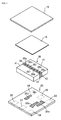
- FIG. 1 illustrates an exploded perspective view of a two-port isolator as a first example of the non-reciprocal circuit device according to the invention.
- the two-port isolator is a lumped constant type isolator, and roughly contains a planar yoke 10, a circuit board 20, a ferrite-magnet assembly containing a ferrite 32 and permanent magnets 41.
- the diagonally shaded part is a conductor.
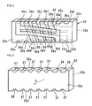
- a ferrite 32 is provided with a first center electrode 35 and a second center electrode 36 that are electrically insulated from each other on first and second principal surfaces 32a and 32b of the front and rear surfaces.
- the ferrite 32 has a rectangular parallelepiped shape having the first principal surface 32a and the second principal surface 32b that are facing each other and are in parallel to each other and has end surfaces (upper surface 32c and lower surface 32d).
- the permanent magnets 41 are adhered to the ferrite 32 through, for example, an epoxy adhesive 42 ( FIG. 4 ) in such a manner as to face the principal surfaces 32a and 32b so that a DC magnetic field is applied in a substantially perpendicular direction to the principal surfaces 32a and 32b to thereby form the ferrite-magnet assembly 30.
- a principal surface 41a of the permanent magnets 41 have the same dimensions as the principal surfaces 32a and 32b of the ferrite 32.
- the principal surfaces 32a and 41a and the principal surfaces 32b and 41a are disposed in such a manner as to face each other so that the outer shapes line up with each other.
- the first center electrode 35 is formed of a conductive film. More specifically, as illustrated in FIG. 2 , the first center electrode 35 extends upward from a lower right section of the first principal surface 32a of the ferrite 32 and bifurcates into two segments. The two segments extend in an upward left direction at a relatively small angle with respect to the longitudinal direction. The first center electrode 35 then extends upward to an upper left section and turns toward the second principal surface 32b through an intermediate electrode 35a on an upper surface 32c. On the second principal surface 32b, the first center electrode 35 bifurcates into two segments so as to overlap with that in the perspective view. One end of the first center electrode 35 is connected to a connector electrode 35b provided on the lower surface 32d.
- the other end of the first center electrode 35 is connected to a connector electrode 35c provided on the lower surface 32d.
- the first center electrode 35 is thus wound around the ferrite 32 by one turn.
- the first center electrode 35 and the second center electrode 36 which will be described below, have an insulating film provided therebetween, such that these electrodes intersect each other while being insulated from each other.
- the second center electrode 36 is also formed of a conductive film.
- the second center electrode 36 has a half-turn segment 36a that extends in the upward left direction from a lower right section of the first principal surface 32a at a relatively large angle with respect to the longitudinal direction and intersects the first center electrode 35.
- the half-turn segment 36a turns towards the second principal surface 32b through an intermediate electrode 36b on the upper surface 32c.
- a 1st-turn segment 36c intersects the first center electrode 35 in a substantially perpendicular manner.
- a lower end portion of the 1st-turn segment 36c turns towards the first principal surface 32a through an intermediate electrode 36d on the lower surface 32d.
- a 1.5-turn segment 36e extends substantially parallel to the half-turn segment 36a and intersects the first center electrode 35 on the first principal surface 32a.
- the 1.5-turn segment 36e turns toward the second principal surface 32b through an intermediate electrode 36f on the upper surface 32c.
- a 2nd-turn segment 36g, an intermediate electrode 36h, a 2.5th-turn segment 36i, an intermediate electrode 36j, a 3rd-turn segment 36k, an intermediate electrode 361, a 3.5th-turn segment 36m, an intermediate electrode 36n, and a 4th-turn segment 36o are provided on the corresponding surfaces of the ferrite 32.
- Both ends of the second center electrode 36 are respectively connected to connector electrodes 35c and 36p provided on the lower surface 32d of the ferrite 32.
- the connector electrode 35c is commonly used as a connector electrode for the ends of the first center electrode 35 and the second center electrode 36.
- the second center electrode 36 is helically wound around the ferrite 32 by four turns.
- the number of turns is calculated on the basis of the fact that one crossing of the center electrode 36 across the first principal surface 32a or the second principal surface 32b equals a 0.5 turn.
- the intersection angle between the center electrodes 35 and 36 is set as required so as to adjust the input impedance and the insertion loss.
- the connector electrodes 35b, 35c, and 36p and the intermediate electrodes 35a, 36b, 36d, 36f, 36h, 36j, 361, and 36n are provided by embedding electrode conductors, such as silver, silver alloy, copper, and copper alloy, into corresponding recesses 37 ( FIG. 3 ) provided in the upper and lower surfaces 32c and 32d of the ferrite 32.
- the upper and lower surfaces 32c and 32d have dummy recesses 38 provided in parallel to the electrodes, and are also provided with dummy electrodes 39a, 39b, and 39c.
- These electrodes are provided by preliminarily providing through holes in a mother ferrite substrate, embedding electrode conductors into these through holes, and then cutting the substrate along where the through holes are to be cut.
- the recesses 37 and 38 have a substantially semicircular shape in cross section or a substantially oval shape in cross section and their openings face the first and second principal surfaces 32a and 32b.
- the opening portion at the downstream side (the first principal surface 32a side) of an application direction A of DC magnetic field by the permanent magnets 41 and 41 is larger than the opening portion at the upstream side (the second principal surface 32b side). More specifically, the recesses 37 and 38 taper toward the opening portion at the downstream side (the first principal surface 32a side) from the opening portion at the upstream side (the second principal surface 32b side). The effects obtained by the recesses 37 and 38 having such a shape will be described later.
- the first and second center electrodes 35 and 36 and the other various electrodes are provided as a thick film or a thin film composed of silver or a silver alloy by, for example, printing, transferring, or photolithography.
- the insulating film between the center electrodes 35 and 36 may be formed of a thick glass or alumina dielectric film or polyimide resin film. These insulating films can also be provided by, for example, printing, transferring, or photolithography.
- the ferrite 32 including the insulating film and various electrodes can be collectively baked using a magnetic material.
- Pd or Pd/Ag that are tolerant of baking at high temperatures is used as the various electrodes.
- thermosetting epoxy adhesive is optimally used as the adhesive 42 that adheres the permanent magnets 41 and the ferrite 32.
- the circuit board 20 is a sintered multilayer substrate having given electrodes provided on a plurality of dielectric sheets.
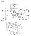
- the circuit board 20 includes matching capacitors C1, C2, Cs1, Cs2, Cp1, and Cp2 illustrated in the equivalent circuits of FIGS. 5 and 6 .
- the terminal resistance R is externally mounted on the circuit board 20.
- the circuit board 20 also includes terminal electrodes 25a, 25b, and 25c on the upper surface thereof and external-connection terminal electrodes 26, 27, and 28 on the lower surface thereof.
- connection relationships between these matching circuit elements and the first and second center electrodes 35 and 36 are as illustrated in FIG. 5 illustrating a first circuit example and FIG. 6 illustrating a second circuit example.
- the connection relationships will be described on the basis of the first circuit example illustrated in FIG. 5 .
- the external-connection terminal electrode 26 provided on the lower surface of the circuit board 20 functions as an input port P1, and is connected to the matching capacitor C1 and the terminal resistor R.
- the terminal electrode 26 is connected to one end of the first center electrode 35 through the terminal electrode 25a provided on the upper surface of the circuit board 20 and the connector electrode 35b provided on the lower surface 32d of the ferrite 32.
- the other end of the first center electrode 35 and one end of the second center electrode 36 are connected to the terminal resistor R and the matching capacitors C1 and C2 through the connector electrode 35c provided on the lower surface 32d of the ferrite 32 and the terminal electrode 25b provided on the upper surface of the circuit board 20, and are also connected to the external-connection terminal electrode 27 provided on the lower surface of the circuit board 20.
- the terminal electrode 27 functions as an output port P2.
- the other end of the second center electrode 36 is connected to the capacitor C2 and the external-connection terminal electrode 28 provided on the lower surface of the circuit board 20 through the connector electrode 36p provided on the lower surface 32d of the ferrite 32 and the terminal electrode 25c provided on the upper surface of the circuit board 20.
- the electrode 28 functions as a ground port P3.
- the capacitors Cs1 and Cp1 are connected to the input port P1 side and the capacitors Cs2 and Cp2 are connected to the output port P2 side. These capacitors are used for impedance adjustment.
- the ferrite-magnet assembly 30 is mounted on the circuit board 20.
- Various electrodes at the lower surface 32d of the ferrite 32 are unified with the terminal electrodes 25a, 25b, and 25c on the circuit board 20 by reflow soldering or the like and the lower surfaces of the permanent magnets 41 are unified with the circuit board 20 with an adhesive.
- the planar yoke 10 has an electromagnetic shielding function.
- the yoke 10 is fixed to the upper surface of the ferrite-magnet assembly 30 through the dielectric layer (adhesive layer) 15.
- the planar yoke 10 has functions of suppressing magnetic leakage and high-frequency electromagnetic field leakage from the ferrite-magnet assembly 30, of suppressing magnetic influences from the external environment, and of providing a portion to be taken up by a vacuum nozzle when this isolator is mounted on a substrate, not shown, using a chip mounter.
- the planar yoke 10 does not have to be grounded and may be grounded by soldering or a conductive adhesive. When grounded, the yoke 10 improves the effect of high-frequency shielding.
- the recesses 37 and 38 provided in the upper and lower surface 32c and 32d of the ferrite 32 are provided in such a manner that the opening portion at the downstream side (the first principal surface 32a side) of an application direction A of DC magnetic field by the permanent magnets 41 and 41 is larger than the opening portion at the upstream side (the second principal surface 32b side). More specifically, the recesses 37 and 38 taper toward the opening portion at the downstream side (the first principal surface 32a side) from the opening portion at the upstream side (the second principal surface 32b side).
- the through holes are provided by blasting or laser beam processing.
- the blasting the recesses 37 and 38 are obtained by spraying fine particles of minute particle diameters to the surface of the matrix through a mask to thereby form tapered through holes at non-masking portions, and cutting the through holes.
- the laser beam processing the recesses 37 and 38 are obtained by irradiating the surface of the matrix of the ferrite 32 with a laser to thereby form tapered through holes at given portions, and the through holes are then cut.
- a conductive material is embedded in the recesses 37 and 38 and a DC magnetic field is applied to the opening portion having a large area from the opening portion having a small area by the permanent magnets 41 and 41.
- a magnetic field distribution simulated by the present inventors using the model illustrated in FIG. 7 is illustrated in FIG. 8 .
- the model illustrated in FIG. 7 is structured so that, on the assumption that the recess 37 smoothly penetrates in a tapered manner toward the first principal surface 32a from the second principal surface 32b in the upper surface 32c of the ferrite 32, the opening portion at the first principal surface 32a side is large and the opening portion at the second principal surface 32b side is small, and then a conductive material is embedded therein, and that a magnetic field distribution at a plane B at the center of the tapered portion is observed.
- FIG. 8(A) illustrates simulation results of the magnetic field distribution at the plane B when the applying direction A of the DC magnetic field by the permanent magnets 41 and 41 is set to a direction from the small opening portion side to the large opening portion side (first example).
- FIG. 8(B) illustrates simulation results of the magnetic field distribution planar at the plane B when the applying direction A of DC magnetic field by the permanent magnets 41 and 41 is set to an opposite direction from the large opening portion side to the small opening portion side (first comparative example).
- FIG. 8(C) illustrates simulation results of the magnetic field distribution at the plane B when the recess 37 is formed in a straight shape having the same diameter as the opening portion of the first principal surface 32a, instead of the tapered shape (second comparative example).
- FIG. 9(A) illustrates insertion loss characteristics of the isolator and FIG. 9(B) illustrates isolation characteristics.
- a curve D1 illustrates characteristics of the first example ( FIG. 8(A) )
- a curve D2 illustrates characteristics of the first comparative example ( FIG. 8(B) ).
- the characteristics of the second comparative example are almost in agreement with the curve D2.
- the magnetic field is hardly disturbed compared with the first and second comparative examples, and thus the insertion loss and isolation in the 800 MHz band are improved.
- the recesses 37 and 38 are smoothly tapered, the disturbance of magnetic field distribution in the ferrite 32 can be suppressed to the minimum, and favorable properties can be obtained.
- the ferrite-magnet assembly 30 is structurally stable because the ferrite 32 and a pair of permanent magnets 41 are unified with the adhesive 42, and thus serves as a strong isolator that is not deformed and damaged by vibration or an impact.
- the circuit board 20 is constituted by a multi-layer dielectric substrate. Accordingly, a circuit network including capacitors and resistors can be included in the circuit board 20. Thus, a small and thin isolator can be achieved, and an increase in reliability can be expected because circuit devices are connected to one another in the circuit board 20. It is a matter of course that the circuit board 20 is not necessarily a multilayer substrate, and may be a single-layer substrate. Furthermore, matching capacitors or the like may be externally mounted as chip type capacitors.
- FIG. 10 illustrates an essential portion of a three-port isolator as a second example of the non-reciprocal circuit device according to the invention and FIG. 11 illustrates an equivalent circuit thereof.
- FIG. 10 illustrates a center electrode assembly 130 in which center electrodes 121, 122, and 123 each having two electrodes are provided using a conductor film on a first principal surface 132a of a ferrite 132 through insulating films 125 and 126.
- a permanent magnet is located at the first principal surface 132a side, and a DC magnetic field is applied in a direction substantially orthogonal to the first principal surface 132a (arrow A).
- a ground pattern is provided substantially over the surface.
- Both ends of each of the center electrodes 121, 122, and 123 are extended to the second principal surface 132b by a connector electrode formed of a conductive material embedded in recesses 137 and 138 provided at four end surfaces 132c of the ferrite 132.
- each of the center electrodes 121, 122, and 123 is electrically connected to the ground pattern through the electrodes embedded in the recesses 137 and the other end of each of the center electrodes 121, 122, and 123 faces the second principal surface 132b through the electrodes embedded in the recesses 138, but is electrically separated from the ground pattern by gaps 128.
- a matching capacitor C11 is inserted in parallel with the center electrode 122 between the port P1 and the ground pattern.
- a matching capacitor C12 is inserted in parallel with the center electrode 121 between the port P2 and the ground pattern.
- a matching capacitor C13 is inserted in parallel with the center electrode 121 between the port P3 and the ground pattern.
- Patent Document 2 Japanese Unexamined Patent Application Publication No. 2002-076711 .
- the recesses 137 and 138 open facing the first and second principal surfaces 132a and 132b of the ferrite 132.
- the opening portion at the downstream side (the second principal surface 132b side) of the application direction A of DC magnetic field by the permanent magnets is larger than the opening portion at the upstream side (the first principal surface 132a side).
- the recesses 137 and 138 smoothly taper toward the opening portion at the downstream side (the second principal surface 132b side) from the opening portion at the upstream side (the first principal surface 132a side). Accordingly, similarly as in the first example, the disturbance of magnetic field distribution in the ferrite decreases to thereby reduce insertion loss and increase isolation.
- the recesses provided in the end surface orthogonal to the first and second principal surfaces of the ferrite are formed in a shape in which the opening portion at the downstream side of the applying direction of DC magnetic field by the permanent magnets is larger than the opening portion at the upstream side thereof.
- the recess tapers toward the opening portion at the downstream side of the applying direction of DC magnetic field from the opening portion at the upstream side thereof.
- the disturbance of magnetic field distribution in the ferrite can be minimized.
- the non-reciprocal circuit device according to the invention is not limited to the examples above, and can be variously changed within the scope of the invention.
- the input port P1 and the output port P2 are interchanged.
- the shapes of the first and second center electrodes 35 and 36 can be variously changed.
- the first example describes that the first center electrode 35 is bifurcated into two segments on the principal surfaces 32a and 32b of the ferrite 32, but may not be bifurcated into two segments.
- the second center electrode 36 may be wound by at least one turn.
- the invention is useful for a non-reciprocal circuit device, and is excellent particularly in that the disturbance of magnetic field distribution in the ferrite decreases to thereby improve insertion loss characteristics and isolation characteristics.
Landscapes
- Non-Reversible Transmitting Devices (AREA)
- Coils Or Transformers For Communication (AREA)
Abstract
Description
- The present invention relates to non-reciprocal circuit devices, and, more particularly, to non-reciprocal circuit devices, such as isolators or circulators, for use in the microwave band.
- In general, non-reciprocal circuit devices, such as isolators or circulators, have a characteristic of transmitting a signal only in a given direction but not in the opposite direction. By utilizing this characteristic, for example, isolators are used in transmitting circuits of mobile communication devices, such as automobile phones and cellular phones.
- As a non-reciprocal circuit device of the type described above, a two-port isolator is known, in which, as described in
Patent Document 1, first and second center electrodes are provided on first and second principal surfaces, which face each other, of a ferrite, and the first and second center electrodes are electrically connected at the first and second principal surface sides, respectively, through a conductive material that has been embedded in a recess provided in the end surface of the ferrite. Moreover, a three-port isolator is known in which, as described inPatent Document 2, the conductive material that has been embedded in the recess provided in the end surface of the ferrite is electrically connected to the center electrodes. - In isolators, a DC magnetic field is applied to a ferrite from permanent magnets. Isolators have problems in that, when a recess is provided in a ferrite, and then a conductive material is embedded therein, a magnetic field distribution in the ferrite is disturbed depending on the shape of the recess and insertion loss characteristics and isolation characteristics are deteriorated.
- [Patent Document 1] International Publication No.
2007/046229 , pamphlet - [Patent Document 2] Japanese Unexamined Patent Application Publication No.
2002-076711 - It is an object of the invention to provide a non-reciprocal circuit device capable of reducing the disturbance of magnetic field distribution in the ferrite and improving insertion loss characteristics and isolation characteristics by appropriately determining the shape of the recess provided in the ferrite so as to embed a conductor therein.
- In order to achieve the object, a non-reciprocal circuit device according to an aspect of the invention, has:
- permanent magnets;
- a ferrite to which a DC magnetic field is applied by the permanent magnets; and
- a plurality of center electrodes formed of conductor films that are disposed on first and second principal surfaces facing each other of the ferrite in such a manner as to intersect each other while being electrically insulated,
- a conductive material being embedded in a recess provided in an end surface orthogonal to the first and second principal surfaces of the ferrite,
- the center electrodes being electrically connected to the conductive material, and
- opening portions facing the first and second principal surfaces of the recess being provided in such a manner that the opening portion at a downstream side of a direction of applying a DC magnetic field by the permanent magnets is larger than the opening portion at an upstream side thereof.
- According to the invention, by appropriately determining the shape of the recess provided in the ferrite so as to embed a conductive material therein, the disturbance of magnetic field distribution in the ferrite decreases to reduce insertion loss and increase isolation characteristics.
-
- [
FIG. 1] FIG. 1 is an exploded perspective view of a first example (two-port isolator) of a non-reciprocal circuit device according to the invention. - [
FIG. 2] FIG. 2 is a perspective view of a ferrite having center electrodes. - [
FIG. 3] FIG. 3 is a perspective view of the ferrite. - [
FIG. 4] FIG. 4 is an exploded perspective view of a ferrite-magnet assembly. - [
FIG. 5] FIG. 5 is an equivalent circuit diagram of a first circuit example of a two-port isolator. - [
FIG. 6] FIG. 6 is an equivalent circuit diagram of a second circuit example of a two-port isolator. - [
FIG. 7] FIG. 7 is a view for illustrating a model for simulating a magnetic field distribution in a ferrite. - [
FIG. 8] FIGS. 8(A), 8(B), and 8(C) are schematic views of the magnetic field distribution in the ferrite, in whichFIG. 8(A) illustrates a first example,FIG. 8(B) illustrates a first comparative example, andFIG. 8(c) illustrates a second comparative example. - [
FIG. 9] FIG. 9(A) is a graph illustrating insertion loss characteristics andFIG. 9(B) is a graph illustrating isolation characteristics. - [
FIG. 10] FIG. 10 is a perspective view of an essential part of a second example (three-port isolator) of the non-reciprocal circuit device according to the invention. - [
FIG. 11] FIG. 11 is equivalent circuit diagram of a three-port isolator. -
- 20
- circuit board
- 30
- ferrite-magnet assembly
- 32,132
- ferrite
- 32a, 32b, 132a, and 132b
- principal surface
- 35
- first center electrode
- 36
- second center electrode
- 37, 38, 137, 138
- recess
- 41
- permanent magnet
- 121, 122, 123
- center electrode
- P1
- input port
- P2
- output port
- P3
- ground port
- Hereinafter, examples of a non-reciprocal circuit device according to the invention will be described with reference to the attached drawings.
-
FIG. 1 illustrates an exploded perspective view of a two-port isolator as a first example of the non-reciprocal circuit device according to the invention. The two-port isolator is a lumped constant type isolator, and roughly contains aplanar yoke 10, acircuit board 20, a ferrite-magnet assembly containing aferrite 32 andpermanent magnets 41. InFIG. 1 , the diagonally shaded part is a conductor. - As illustrated in
FIG. 2 , aferrite 32 is provided with afirst center electrode 35 and asecond center electrode 36 that are electrically insulated from each other on first and secondprincipal surfaces ferrite 32 has a rectangular parallelepiped shape having the firstprincipal surface 32a and the secondprincipal surface 32b that are facing each other and are in parallel to each other and has end surfaces (upper surface 32c andlower surface 32d). - The
permanent magnets 41 are adhered to theferrite 32 through, for example, an epoxy adhesive 42 (FIG. 4 ) in such a manner as to face theprincipal surfaces principal surfaces magnet assembly 30. Aprincipal surface 41a of thepermanent magnets 41 have the same dimensions as theprincipal surfaces ferrite 32. The principal surfaces 32a and 41a and theprincipal surfaces - The
first center electrode 35 is formed of a conductive film. More specifically, as illustrated inFIG. 2 , thefirst center electrode 35 extends upward from a lower right section of the firstprincipal surface 32a of theferrite 32 and bifurcates into two segments. The two segments extend in an upward left direction at a relatively small angle with respect to the longitudinal direction. Thefirst center electrode 35 then extends upward to an upper left section and turns toward the secondprincipal surface 32b through anintermediate electrode 35a on anupper surface 32c. On the secondprincipal surface 32b, thefirst center electrode 35 bifurcates into two segments so as to overlap with that in the perspective view. One end of thefirst center electrode 35 is connected to aconnector electrode 35b provided on thelower surface 32d. The other end of thefirst center electrode 35 is connected to aconnector electrode 35c provided on thelower surface 32d. Thefirst center electrode 35 is thus wound around theferrite 32 by one turn. Thefirst center electrode 35 and thesecond center electrode 36, which will be described below, have an insulating film provided therebetween, such that these electrodes intersect each other while being insulated from each other. - The
second center electrode 36 is also formed of a conductive film. Thesecond center electrode 36 has a half-turn segment 36a that extends in the upward left direction from a lower right section of the firstprincipal surface 32a at a relatively large angle with respect to the longitudinal direction and intersects thefirst center electrode 35. The half-turn segment 36a turns towards the secondprincipal surface 32b through an intermediate electrode 36b on theupper surface 32c. On the secondprincipal surface 32b, a 1st-turn segment 36c intersects thefirst center electrode 35 in a substantially perpendicular manner. A lower end portion of the 1st-turn segment 36c turns towards the firstprincipal surface 32a through anintermediate electrode 36d on thelower surface 32d. On the firstprincipal surface 32a, a 1.5-turn segment 36e extends substantially parallel to the half-turn segment 36a and intersects thefirst center electrode 35 on the firstprincipal surface 32a. The 1.5-turn segment 36e turns toward the secondprincipal surface 32b through anintermediate electrode 36f on theupper surface 32c. In a similar manner, a 2nd-turn segment 36g, anintermediate electrode 36h, a 2.5th-turn segment 36i, an intermediate electrode 36j, a 3rd-turn segment 36k, anintermediate electrode 361, a 3.5th-turn segment 36m, anintermediate electrode 36n, and a 4th-turn segment 36o are provided on the corresponding surfaces of theferrite 32. Both ends of thesecond center electrode 36 are respectively connected toconnector electrodes lower surface 32d of theferrite 32. Theconnector electrode 35c is commonly used as a connector electrode for the ends of thefirst center electrode 35 and thesecond center electrode 36. - More specifically, the
second center electrode 36 is helically wound around theferrite 32 by four turns.
Here, the number of turns is calculated on the basis of the fact that one crossing of thecenter electrode 36 across the firstprincipal surface 32a or the secondprincipal surface 32b equals a 0.5 turn. The intersection angle between thecenter electrodes - The
connector electrodes intermediate electrodes FIG. 3 ) provided in the upper andlower surfaces ferrite 32.
In addition, the upper andlower surfaces dummy electrodes - The
recesses principal surfaces principal surface 32a side) of an application direction A of DC magnetic field by thepermanent magnets principal surface 32b side). More specifically, therecesses principal surface 32a side) from the opening portion at the upstream side (the secondprincipal surface 32b side). The effects obtained by therecesses - As the
ferrite 32, a YIG ferrite or the like may be used. The first andsecond center electrodes
The insulating film between thecenter electrodes - The
ferrite 32 including the insulating film and various electrodes can be collectively baked using a magnetic material. In such a case, Pd or Pd/Ag that are tolerant of baking at high temperatures is used as the various electrodes. - For the
permanent magnets 41, strontium, barium, or lanthanum-cobalt ferrite magnets are generally used. A one-part thermosetting epoxy adhesive is optimally used as the adhesive 42 that adheres thepermanent magnets 41 and theferrite 32. - The
circuit board 20 is a sintered multilayer substrate having given electrodes provided on a plurality of dielectric sheets. Thecircuit board 20 includes matching capacitors C1, C2, Cs1, Cs2, Cp1, and Cp2 illustrated in the equivalent circuits ofFIGS. 5 and6 . The terminal resistance R is externally mounted on thecircuit board 20. Thecircuit board 20 also includesterminal electrodes connection terminal electrodes - The connection relationships between these matching circuit elements and the first and
second center electrodes FIG. 5 illustrating a first circuit example andFIG. 6 illustrating a second circuit example. Here, the connection relationships will be described on the basis of the first circuit example illustrated inFIG. 5 . - The external-
connection terminal electrode 26 provided on the lower surface of thecircuit board 20 functions as an input port P1, and is connected to the matching capacitor C1 and the terminal resistor R. Theterminal electrode 26 is connected to one end of thefirst center electrode 35 through theterminal electrode 25a provided on the upper surface of thecircuit board 20 and theconnector electrode 35b provided on thelower surface 32d of theferrite 32. - The other end of the
first center electrode 35 and one end of thesecond center electrode 36 are connected to the terminal resistor R and the matching capacitors C1 and C2 through theconnector electrode 35c provided on thelower surface 32d of theferrite 32 and theterminal electrode 25b provided on the upper surface of thecircuit board 20, and are also connected to the external-connection terminal electrode 27 provided on the lower surface of thecircuit board 20. Theterminal electrode 27 functions as an output port P2. - The other end of the
second center electrode 36 is connected to the capacitor C2 and the external-connection terminal electrode 28 provided on the lower surface of thecircuit board 20 through theconnector electrode 36p provided on thelower surface 32d of theferrite 32 and theterminal electrode 25c provided on the upper surface of thecircuit board 20. Theelectrode 28 functions as a ground port P3. - In the second circuit example illustrated in
FIG. 6 , the capacitors Cs1 and Cp1 are connected to the input port P1 side and the capacitors Cs2 and Cp2 are connected to the output port P2 side. These capacitors are used for impedance adjustment. - The ferrite-
magnet assembly 30 is mounted on thecircuit board 20. Various electrodes at thelower surface 32d of theferrite 32 are unified with theterminal electrodes circuit board 20 by reflow soldering or the like and the lower surfaces of thepermanent magnets 41 are unified with thecircuit board 20 with an adhesive. - The
planar yoke 10 has an electromagnetic shielding function. Theyoke 10 is fixed to the upper surface of the ferrite-magnet assembly 30 through the dielectric layer (adhesive layer) 15. Theplanar yoke 10 has functions of suppressing magnetic leakage and high-frequency electromagnetic field leakage from the ferrite-magnet assembly 30, of suppressing magnetic influences from the external environment, and of providing a portion to be taken up by a vacuum nozzle when this isolator is mounted on a substrate, not shown, using a chip mounter. Theplanar yoke 10 does not have to be grounded and may be grounded by soldering or a conductive adhesive. When grounded, theyoke 10 improves the effect of high-frequency shielding. - In the two-port isolator having the structure described above, since one end of the
first center electrode 35 is connected to the input port P1, the other end of thefirst center electrode 35 is connected to the output port P2, one end of thesecond center electrode 36 is connected to the output port P2, and the other end of thesecond center electrode 36 is connected to the ground port P3, a two-port lumped-parameter isolator having a small insertion loss can be obtained. In addition, during operation of the isolator, a large amount of high-frequency current is supplied to thesecond center electrode 36 whereas a negligible amount of high frequency current is supplied to thefirst center electrode 35. Therefore, a direction of a high-frequency field generated using thefirst center electrode 35 and thesecond center electrode 36 depends on an arrangement of thesecond center electrode 36. Measures to reduce the insertion loss are readily performed when the direction of the high-frequency field is determined. - In the first example, as illustrated in
FIG. 2 , therecesses lower surface ferrite 32 are provided in such a manner that the opening portion at the downstream side (the firstprincipal surface 32a side) of an application direction A of DC magnetic field by thepermanent magnets principal surface 32b side). More specifically, therecesses principal surface 32a side) from the opening portion at the upstream side (the secondprincipal surface 32b side). - When such recesses 37 and 38 form the through holes in the matrix of the
ferrite 32, the through holes are provided by blasting or laser beam processing. With the blasting, therecesses recesses ferrite 32 with a laser to thereby form tapered through holes at given portions, and the through holes are then cut. - A conductive material is embedded in the
recesses permanent magnets ferrite 32 is reduced. Here, a magnetic field distribution simulated by the present inventors using the model illustrated inFIG. 7 is illustrated inFIG. 8 . - The model illustrated in
FIG. 7 is structured so that, on the assumption that therecess 37 smoothly penetrates in a tapered manner toward the firstprincipal surface 32a from the secondprincipal surface 32b in theupper surface 32c of theferrite 32, the opening portion at the firstprincipal surface 32a side is large and the opening portion at the secondprincipal surface 32b side is small, and then a conductive material is embedded therein, and that a magnetic field distribution at a plane B at the center of the tapered portion is observed. -
FIG. 8(A) illustrates simulation results of the magnetic field distribution at the plane B when the applying direction A of the DC magnetic field by thepermanent magnets FIG. 8(B) illustrates simulation results of the magnetic field distribution planar at the plane B when the applying direction A of DC magnetic field by thepermanent magnets FIG. 8(C) illustrates simulation results of the magnetic field distribution at the plane B when therecess 37 is formed in a straight shape having the same diameter as the opening portion of the firstprincipal surface 32a, instead of the tapered shape (second comparative example). In the first and second comparative examples (FIGS. 8(B) and 8(C) ), the magnetic field distribution disturbs in a portion (portion near the recess 37) surrounded by the dotted line C. In contrast, such disturbance of magnetic field does not arise in the first example (FIG. 8(A) ). -
FIG. 9(A) illustrates insertion loss characteristics of the isolator andFIG. 9(B) illustrates isolation characteristics. In bothFIGS. 9(A) and 9(B) , a curve D1 illustrates characteristics of the first example (FIG. 8(A) ), and a curve D2 illustrates characteristics of the first comparative example (FIG. 8(B) ). The characteristics of the second comparative example are almost in agreement with the curve D2. In the first example, the magnetic field is hardly disturbed compared with the first and second comparative examples, and thus the insertion loss and isolation in the 800 MHz band are improved. In particular, since therecesses ferrite 32 can be suppressed to the minimum, and favorable properties can be obtained. - In the first example, the ferrite-
magnet assembly 30 is structurally stable because theferrite 32 and a pair ofpermanent magnets 41 are unified with the adhesive 42, and thus serves as a strong isolator that is not deformed and damaged by vibration or an impact. - The
circuit board 20 is constituted by a multi-layer dielectric substrate. Accordingly, a circuit network including capacitors and resistors can be included in thecircuit board 20. Thus, a small and thin isolator can be achieved, and an increase in reliability can be expected because circuit devices are connected to one another in thecircuit board 20. It is a matter of course that thecircuit board 20 is not necessarily a multilayer substrate, and may be a single-layer substrate. Furthermore, matching capacitors or the like may be externally mounted as chip type capacitors. -
FIG. 10 illustrates an essential portion of a three-port isolator as a second example of the non-reciprocal circuit device according to the invention andFIG. 11 illustrates an equivalent circuit thereof.FIG. 10 illustrates acenter electrode assembly 130 in which centerelectrodes principal surface 132a of aferrite 132 through insulatingfilms - To the
center electrode assembly 130, a permanent magnet, not illustrated, is located at the firstprincipal surface 132a side, and a DC magnetic field is applied in a direction substantially orthogonal to the firstprincipal surface 132a (arrow A). On a secondprincipal surface 132b of theferrite 132, a ground pattern is provided substantially over the surface. Both ends of each of thecenter electrodes principal surface 132b by a connector electrode formed of a conductive material embedded inrecesses end surfaces 132c of theferrite 132. One end of each of thecenter electrodes recesses 137 and the other end of each of thecenter electrodes principal surface 132b through the electrodes embedded in therecesses 138, but is electrically separated from the ground pattern bygaps 128. - Moreover, as illustrated in the equivalent circuit of
FIG. 11 , a matching capacitor C11 is inserted in parallel with thecenter electrode 122 between the port P1 and the ground pattern. A matching capacitor C12 is inserted in parallel with thecenter electrode 121 between the port P2 and the ground pattern. A matching capacitor C13 is inserted in parallel with thecenter electrode 121 between the port P3 and the ground pattern. - The structure of such a non-reciprocal circuit device is described in detail in Patent Document 2 (Japanese Unexamined Patent Application Publication No.
2002-076711 - Similarly as in the first example, the
recesses principal surfaces ferrite 132. The opening portion at the downstream side (the secondprincipal surface 132b side) of the application direction A of DC magnetic field by the permanent magnets is larger than the opening portion at the upstream side (the firstprincipal surface 132a side). More specifically, therecesses principal surface 132b side) from the opening portion at the upstream side (the firstprincipal surface 132a side). Accordingly, similarly as in the first example, the disturbance of magnetic field distribution in the ferrite decreases to thereby reduce insertion loss and increase isolation. - In the above-described non-reciprocal circuit device, in order to embed the conductive material for connection with the center electrodes, the recesses provided in the end surface orthogonal to the first and second principal surfaces of the ferrite are formed in a shape in which the opening portion at the downstream side of the applying direction of DC magnetic field by the permanent magnets is larger than the opening portion at the upstream side thereof. Thus, the disturbance of magnetic field distribution in the ferrite decreases to thereby improve insertion loss characteristics and isolation characteristics.
- In particular, by electrically connecting the first center electrode and the second center electrode with the conductive material embedded in the recess and winding them around the ferrite, a two-port lumped constant type isolator having small insertion loss can be obtained.
- Preferably, the recess tapers toward the opening portion at the downstream side of the applying direction of DC magnetic field from the opening portion at the upstream side thereof. The disturbance of magnetic field distribution in the ferrite can be minimized.
- The non-reciprocal circuit device according to the invention is not limited to the examples above, and can be variously changed within the scope of the invention.
- For example, when the N pole and the S pole of the
permanent magnets 41 are reversed, the input port P1 and the output port P2 are interchanged. The shapes of the first andsecond center electrodes first center electrode 35 is bifurcated into two segments on theprincipal surfaces ferrite 32, but may not be bifurcated into two segments. Thesecond center electrode 36 may be wound by at least one turn. - As described above, the invention is useful for a non-reciprocal circuit device, and is excellent particularly in that the disturbance of magnetic field distribution in the ferrite decreases to thereby improve insertion loss characteristics and isolation characteristics.
Claims (5)
- A non-reciprocal circuit device, comprising:permanent magnets;a ferrite to which a DC magnetic field is applied by the permanent magnets; anda plurality of center electrodes formed of conductor films that are disposed on first and second principal surfaces of the ferrite that face each other in such a manner as to intersect each other while being electrically insulated from one another,a conductive material that is embedded in a recess provided in an end surface orthogonal to the first and second principal surfaces of the ferrite,the center electrodes being electrically connected to the conductive material, andopening portions facing the first and second principal surfaces of the recess being provided in such a manner that the opening portion at a downstream side of a direction of applying a DC magnetic field by the permanent magnets is larger than the opening portion at an upstream side thereof.
- The non-reciprocal circuit device according to claim 1, wherein
the plurality of center electrodes contain first and second center electrodes,
one end of the first center electrode is electrically connected to an input port and the other end thereof is electrically connected to an output port,
one end of the second center electrode is electrically connected to an output port and the other end thereof is electrically connected to a ground port,
a first matching capacitance is electrically connected between the input port and the output port,
a second matching capacitance is connected between the output port and the ground port, and
a resistance is electrically connected between the input port and the output port. - The non-reciprocal circuit device according to claim 1 or 2, wherein the recess tapers toward the opening portion at the downstream side of the applying direction of DC magnetic field from the opening portion at the upstream side thereof.
- The non-reciprocal circuit device according to claim 1, 2, or 3, wherein the ferrite and the permanent magnets constitute a ferrite-magnet assembly in which the ferrite is sandwiched by a pair of permanent magnets from both sides in parallel with the first and second principal surfaces on which the first and second center electrodes are disposed.
- The non-reciprocal circuit device according to claim 4, further comprising a circuit board having a terminal electrode provided on the surface,
the ferrite-magnet assembly being disposed on the circuit board in such a manner that the first and second principal surfaces are perpendicular to the surface of the circuit board.
Applications Claiming Priority (2)
| Application Number | Priority Date | Filing Date | Title |
|---|---|---|---|
| JP2007227876 | 2007-09-03 | ||
| PCT/JP2008/064130 WO2009031380A1 (en) | 2007-09-03 | 2008-08-06 | Irreversible circuit element |
Publications (2)
| Publication Number | Publication Date |
|---|---|
| EP2187474A1 true EP2187474A1 (en) | 2010-05-19 |
| EP2187474A4 EP2187474A4 (en) | 2010-08-25 |
Family
ID=40428702
Family Applications (1)
| Application Number | Title | Priority Date | Filing Date |
|---|---|---|---|
| EP08828967A Withdrawn EP2187474A4 (en) | 2007-09-03 | 2008-08-06 | Irreversible circuit element |
Country Status (5)
| Country | Link |
|---|---|
| US (1) | US7830222B2 (en) |
| EP (1) | EP2187474A4 (en) |
| JP (1) | JP4760981B2 (en) |
| CN (1) | CN101785140B (en) |
| WO (1) | WO2009031380A1 (en) |
Families Citing this family (2)
| Publication number | Priority date | Publication date | Assignee | Title |
|---|---|---|---|---|
| US11551046B1 (en) * | 2011-10-19 | 2023-01-10 | Dynamics Inc. | Stacked dynamic magnetic stripe commmunications device for magnetic cards and devices |
| WO2014196324A1 (en) * | 2013-06-07 | 2014-12-11 | 株式会社村田製作所 | Non-reciprocal circuit element |
Family Cites Families (9)
| Publication number | Priority date | Publication date | Assignee | Title |
|---|---|---|---|---|
| JP3125693B2 (en) * | 1996-11-14 | 2001-01-22 | 株式会社村田製作所 | Non-reciprocal circuit device |
| JP3384367B2 (en) * | 1999-09-21 | 2003-03-10 | 株式会社村田製作所 | Non-reciprocal circuit device and communication device |
| JP3528771B2 (en) * | 2000-08-25 | 2004-05-24 | 株式会社村田製作所 | Manufacturing method of center electrode assembly |
| JP3649161B2 (en) * | 2000-09-13 | 2005-05-18 | 株式会社村田製作所 | Center electrode assembly, non-reciprocal circuit device, and communication device |
| JP3649144B2 (en) * | 2001-04-10 | 2005-05-18 | 株式会社村田製作所 | Non-reciprocal circuit element, communication apparatus, and non-reciprocal circuit element manufacturing method |
| JP3649162B2 (en) * | 2001-07-06 | 2005-05-18 | 株式会社村田製作所 | Center electrode assembly, non-reciprocal circuit device, communication device, and method of manufacturing center electrode assembly |
| JP3705253B2 (en) * | 2002-08-14 | 2005-10-12 | 株式会社村田製作所 | 3-port non-reciprocal circuit device and communication device |
| JP4345709B2 (en) * | 2005-05-02 | 2009-10-14 | 株式会社村田製作所 | Non-reciprocal circuit device, manufacturing method thereof, and communication device |
| CN100568618C (en) * | 2005-10-21 | 2009-12-09 | 株式会社村田制作所 | Nonreciprocal circuit element, method for manufacturing same and communication device |
-
2008
- 2008-08-06 CN CN2008801039552A patent/CN101785140B/en not_active Expired - Fee Related
- 2008-08-06 EP EP08828967A patent/EP2187474A4/en not_active Withdrawn
- 2008-08-06 WO PCT/JP2008/064130 patent/WO2009031380A1/en not_active Ceased
- 2008-08-06 JP JP2009531165A patent/JP4760981B2/en not_active Expired - Fee Related
-
2010
- 2010-02-05 US US12/700,814 patent/US7830222B2/en active Active
Also Published As
| Publication number | Publication date |
|---|---|
| JPWO2009031380A1 (en) | 2010-12-09 |
| CN101785140B (en) | 2012-12-19 |
| EP2187474A4 (en) | 2010-08-25 |
| US20100127794A1 (en) | 2010-05-27 |
| US7830222B2 (en) | 2010-11-09 |
| CN101785140A (en) | 2010-07-21 |
| JP4760981B2 (en) | 2011-08-31 |
| WO2009031380A1 (en) | 2009-03-12 |
Similar Documents
| Publication | Publication Date | Title |
|---|---|---|
| EP2184802B1 (en) | Irreversible circuit element | |
| JP4656186B2 (en) | Non-reciprocal circuit device and method of manufacturing composite electronic component | |
| EP1939973B1 (en) | Irreversible circuit element, its manufacturing method and communication apparatus | |
| JP5024384B2 (en) | Non-reciprocal circuit element | |
| EP2105987A1 (en) | Non-reversible circuit element and method of manufacturing it | |
| EP2109179A1 (en) | Non-reversible circuit element | |
| JP4155342B1 (en) | Non-reciprocal circuit element | |
| CN101361220B (en) | Non-reversible circuit element | |
| EP2187474A1 (en) | Irreversible circuit element | |
| CN101779328B (en) | nonreciprocal circuit element | |
| JP5098813B2 (en) | Non-reciprocal circuit device and composite electronic component | |
| JP4915366B2 (en) | Non-reciprocal circuit element | |
| JP4929488B2 (en) | Non-reciprocal circuit element | |
| US7859357B2 (en) | Non-reciprocal circuit device | |
| JP5652116B2 (en) | Non-reciprocal circuit element | |
| US20180115038A1 (en) | Non-reciprocal circuit element, high-frequency circuit and communication device | |
| JP2010081394A (en) | Irreversible circuit element and manufacturing method thereof | |
| JP2013038526A (en) | Wiring board for surface mounting non-reciprocal circuit element, and mobile communication equipment including the same |
Legal Events
| Date | Code | Title | Description |
|---|---|---|---|
| PUAI | Public reference made under article 153(3) epc to a published international application that has entered the european phase |
Free format text: ORIGINAL CODE: 0009012 |
|
| 17P | Request for examination filed |
Effective date: 20100126 |
|
| AK | Designated contracting states |
Kind code of ref document: A1 Designated state(s): AT BE BG CH CY CZ DE DK EE ES FI FR GB GR HR HU IE IS IT LI LT LU LV MC MT NL NO PL PT RO SE SI SK TR |
|
| AX | Request for extension of the european patent |
Extension state: AL BA MK RS |
|
| A4 | Supplementary search report drawn up and despatched |
Effective date: 20100723 |
|
| DAX | Request for extension of the european patent (deleted) | ||
| 17Q | First examination report despatched |
Effective date: 20120216 |
|
| GRAP | Despatch of communication of intention to grant a patent |
Free format text: ORIGINAL CODE: EPIDOSNIGR1 |
|
| RIC1 | Information provided on ipc code assigned before grant |
Ipc: H01P 1/36 20060101ALI20160222BHEP Ipc: H01P 1/387 20060101AFI20160222BHEP |
|
| INTG | Intention to grant announced |
Effective date: 20160310 |
|
| STAA | Information on the status of an ep patent application or granted ep patent |
Free format text: STATUS: THE APPLICATION IS DEEMED TO BE WITHDRAWN |
|
| 18D | Application deemed to be withdrawn |
Effective date: 20160721 |