EP2187460A1 - Thermoelectric conversion element and method for manufacturing the same - Google Patents
Thermoelectric conversion element and method for manufacturing the same Download PDFInfo
- Publication number
- EP2187460A1 EP2187460A1 EP08791720A EP08791720A EP2187460A1 EP 2187460 A1 EP2187460 A1 EP 2187460A1 EP 08791720 A EP08791720 A EP 08791720A EP 08791720 A EP08791720 A EP 08791720A EP 2187460 A1 EP2187460 A1 EP 2187460A1
- Authority
- EP
- European Patent Office
- Prior art keywords
- thermoelectric conversion
- conversion device
- ridge
- film
- main body
- Prior art date
- Legal status (The legal status is an assumption and is not a legal conclusion. Google has not performed a legal analysis and makes no representation as to the accuracy of the status listed.)
- Withdrawn
Links
Images





Classifications
-
- H—ELECTRICITY
- H10—SEMICONDUCTOR DEVICES; ELECTRIC SOLID-STATE DEVICES NOT OTHERWISE PROVIDED FOR
- H10N—ELECTRIC SOLID-STATE DEVICES NOT OTHERWISE PROVIDED FOR
- H10N10/00—Thermoelectric devices comprising a junction of dissimilar materials, i.e. devices exhibiting Seebeck or Peltier effects
- H10N10/10—Thermoelectric devices comprising a junction of dissimilar materials, i.e. devices exhibiting Seebeck or Peltier effects operating with only the Peltier or Seebeck effects
- H10N10/17—Thermoelectric devices comprising a junction of dissimilar materials, i.e. devices exhibiting Seebeck or Peltier effects operating with only the Peltier or Seebeck effects characterised by the structure or configuration of the cell or thermocouple forming the device
Definitions
- the present invention relates to thermoelectric conversion devices and production methods thereof.
- thermoelectric conversion devices As thermoelectric conversion devices, a p-type thermoelectric conversion device made of a material such as Ca 3 CO 4 O 9 , Na x CoO 2 , CoSb 3 or BiTeSb and an n-type thermoelectric conversion device made of a material such as SrTiO 3 , BaTiO 3 , Mg 2 Si or CaB 6 have conventionally been known. Further, such thermoelectric conversion devices are often used at high temperature in an atmosphere such as air.
- thermoelectric conversion characteristics of some thermoelectric conversion devices are degraded when subjected to high temperature.
- thermoelectric conversion device main body a thermoelectric conversion device main body by a film of glass or the like ( JP 11-251647 ).
- thermoelectric conversion devices have been made in view of the above-described problems, and its object is to provide thermoelectric conversion devices and production methods thereof, which are capable of reducing the degradation of characteristics in a high temperature environment.
- thermoelectric conversion device main body has a ridge and a vertex, but it is difficult for a film to be sufficiently formed at this ridge or vertex; and the diffusion of an atmospheric gas from an outside atmosphere to a thermoelectric conversion device is likely to occur via the insufficient film at this ridge or vertex, which causes the degradation of the thermoelectric conversion device, and thus reached the concept of the present invention.
- thermoelectric conversion device is a thermoelectric conversion device including: a thermoelectric conversion device main body having a ridge portion and/or a vertex portion at which a ridge and/or a vertex have/has been subjected to a chamfering process; and a film covering a surface of the thermoelectric conversion device main body, including the ridge portion and/or the vertex portion thereof.
- thermoelectric conversion device including: a thermoelectric conversion device main body having a ridge at which two faces meet, and having an angle created by the two faces at the ridge in a cross section taken perpendicularly to the ridge, the angle being an obtuse angle; and a film covering a surface of the thermoelectric conversion device main body, including the ridge.
- the first thermoelectric conversion device has the ridge portion and/or vertex portion at which the ridge and/or vertex have/has been subjected to a chamfering process. Accordingly, the film at the ridge portion and/or vertex portion can be easily formed to a thickness similar to that of the other portion.
- the second thermoelectric conversion device has an obtuse angle at the ridge, and therefore, the film at the ridge can be easily formed to a thickness similar to that of the other portion.
- thermoelectric conversion device main body is likely to oxidize, the diffusion of the atmospheric gas is reduced due to the sufficient formation of the film, thereby enabling the reduction of characteristic degradation in the thermoelectric conversion device.
- the film of the thermoelectric conversion device is preferably an oxidation preventing film.
- an oxidation preventing film Even when subjected to high temperature in an oxidizing atmosphere such as air, the characteristics of the thermoelectric conversion device can be sufficiently maintained, thereby providing the thermoelectric conversion device having high general versatility.
- thermoelectric conversion device is preferably at least one of silica, alumina and silicon carbide.
- the thermoelectric conversion device having excellent oxidation resistance, heat resistance and abrasion resistance can be provided.
- the film of the thermoelectric conversion device preferably has a thickness of 0.01 ⁇ m to 1mm, more preferably has a thickness of 0.1 ⁇ m to 300 ⁇ m, and even more preferably has a thickness of 1 ⁇ m to 100 ⁇ m. If the thickness of the film falls within the foregoing ranges, the diffusion of gas via the film during use at high temperature can be sufficiently reduced. Whereas if the thickness of the film is too small, there is a tendency to make it difficult to reduce the diffusion of gas, and if the thickness is too large, there is a tendency to facilitate occurrence of cracks in the film. Besides, the more uniform the thickness of the film, the better.
- a first method for producing a thermoelectric conversion device includes the steps of: performing a chamfering process on a ridge and/or a vertex of a thermoelectric conversion device main body; and forming a film on a surface of the thermoelectric conversion device main body, including a ridge portion and/or a vertex portion on which the chamfering process has been performed.
- a second method for producing a thermoelectric conversion device includes the steps of: preparing a thermoelectric conversion device main body having a ridge at which two faces meet, and having an angle created by the two faces at the ridge in a cross section taken perpendicularly to the ridge, the angle being an obtuse angle; and forming a film on a surface of the thermoelectric conversion device, including the ridge.
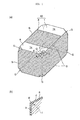
- FIG. 1(a) illustrates a perspective view of one example of a thermoelectric conversion device according to a first embodiment of the present invention.
- the thermoelectric conversion device 10 has vertex portions G, and is almost in the shape of rectangular parallelepiped.
- the thermoelectric conversion device 10 includes a thermoelectric conversion device main body 1, and a film 8 that covers surfaces of the thermoelectric conversion device main body 1.
- one plane a an upper face in FIG. 1(a) ) including the longest ridges B has an exposed portion 1s, at which the thermoelectric conversion device main body 1 is exposed, in respective given ranges from both longitudinal ends of this plane.
- this exposed portion 1s is formed as an electrode connection portion for connecting a plurality of the thermoelectric conversion devices 10 in series.
- FIG. 2 illustrates a perspective view of one example of a conventional thermoelectric conversion device main body.
- the thermoelectric conversion device main body 1 is formed into a rectangular parallelepiped having a plurality of ridges B, and each vertex A is formed at a portion where the three ridges B meet.
- the vertex portions G of the thermoelectric conversion device 10 in FIG. 1(a) are in a state where each vertex A of the thermoelectric conversion device main body 1 in FIG. 2 is C-chamfered, i.e., in a state where each vertex is chamfered by a plane d.
- the vertex portions G in the C-chamfered state each form the plane d surrounded by three ridges E.
- FIG. 1(b) there is illustrated a partial cross-sectional view taken perpendicularly to the ridge E along a dotted line IIb-IIb of the thermoelectric conversion device 10.
- an angle ⁇ created by the two faces b and d, which form the ridge E becomes an obtuse angle greater than 90° by C-chamfering.
- the angle ⁇ is preferably not less than 135°, and is more preferably not less than 157°. If the angle ⁇ is not more than 90° at this ridge E, the film 8 is not formed on the ridge E to a thickness equal to that of a plane portion around the ridge E.
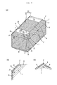
- FIG. 3(a) illustrates a perspective view of another example of a thermoelectric conversion device according to the first embodiment of the present invention.
- the thermoelectric conversion device 10 have C-chamfered ridge portions H, and is almost in the shape of rectangular parallelepiped.
- the ridge portions H of the thermoelectric conversion device 10 in FIG. 3(a) are in a state where each ridge B of the thermoelectric conversion device 10 in FIG. 2 is C-chamfered by a plane e.
- a new vertex I is formed at a point where the three ridge portions H meet.
- a ridge F is formed as a line along which the ridge portions H meet.
- the ridge portions H form the planes e each surrounded by: two ridges J parallel to the original ridge B, and the four ridges F.
- FIG. 3(b) there is illustrated a partial cross-sectional view taken perpendicularly to the axial direction of the ridge portion H along a dotted line IIIb-IIIb of the thermoelectric conversion device 10.
- angles ⁇ and ⁇ each created by the two planes, which form the ridge J, become obtuse angles greater than 90° by chamfering.
- the angles ⁇ and ⁇ ' are each preferably similar to the angle ⁇ . If the angles ⁇ and ⁇ ' are not more than 90°, the film 8 is not formed on the ridges J to a thickness equal to that of a plane portion around the ridges J.
- FIG. 3(c ) there is illustrated a partial cross-sectional view taken perpendicularly to the ridge F along a dotted line IIIc-IIIc of the thermoelectric conversion device 10.
- an angle ⁇ created by the two faces, which form the ridge F becomes an obtuse angle greater than 90° by chamfering.
- FIG. 4 (a) illustrates a perspective view of still another example of a thermoelectric conversion device according to the first embodiment of the present invention.
- the thermoelectric conversion device 10 has vertex portions G and ridge portions H, and is usually formed into a rectangular parallelepiped.
- the thermoelectric conversion device in FIG. 4(a) is in a state where each vertex I of the thermoelectric conversion device 10 in FIG. 3 is further C-chamfered by a plane f, and the plane f of the vertex portion G becomes a plane surrounded by ridges K.
- FIG. 4(b) there is illustrated a partial cross-sectional view taken perpendicularly to the ridge K along a dotted line IVb-IVb of the thermoelectric conversion device 10.
- an angle ⁇ created by two faces e and f, which form the ridge K becomes an obtuse angle greater than 90° by chamfering.
- thermoelectric conversion device main body 1 examples include metal composite oxides such as Ca 3 Co 4 O 9 and Na x CoO 2 ; silicides such as MnSi 1.73, Fe 1-x Mn x Si 2 , Si 0.8 Ge 0.2 and ⁇ -FeSi 2 ; skutterudites such as CoSb 3 , FeSb 3 and RFe 3 CoSb 12 (where R represents La, Ce or Yb); and Te-containing alloys such as BiTeSb, PbTeSb, Bi 2 Te 3 and PbTe.
- metal composite oxides such as Ca 3 Co 4 O 9 and Na x CoO 2
- silicides such as MnSi 1.73, Fe 1-x Mn x Si 2 , Si 0.8 Ge 0.2 and ⁇ -FeSi 2
- skutterudites such as CoSb 3 , FeSb 3 and RFe 3 CoSb 12 (where R represents La, Ce or Yb)
- Te-containing alloys such as Bi
- thermoelectric device materials include metal composite oxides such as SrTiO 3 , Zn 1-x Al x O, CaMnO 3 , LaNiO 3 , Ba x Ti 8 O 16 , BaTiO 3 and Ti 1-x Nb x O; silicides such as Mg 2 Si, Fe 1-x Co x Si 2 , Si 0.8 Ge 0 .
- the present embodiment provides the thermoelectric conversion device 10 including the film 8; therefore, for the thermoelectric conversion device main body 1, a material whose characteristics are likely to degrade due to oxidation in an oxidizing atmosphere or reduction in a non-oxidizing atmosphere within a high temperature environment can be suitably used.
- a material whose characteristics are likely to degrade due to oxidation in an oxidizing atmosphere or reduction in a non-oxidizing atmosphere within a high temperature environment can be suitably used.
- examples of such materials include Zn 4 Sb 3 , CoSb 3 , Bi 2 Te 3 and PbTe as materials for a p-type thermoelectric conversion device, and include SrTiO 3 , Zn 1-x Al x O, BaTiO 3 , Bi 2 Te 3 and PbTe as materials for an n-type thermoelectric device.
- the film 8 is preferably a film including, as a main material, one of silica, alumina and silicon carbide singly or a combination with another or more. Further, the thickness of the film 8 is preferably from 0.01 ⁇ m to 1mm, more preferably from 0.1 ⁇ m to 300 ⁇ m, and even more preferably from 1 ⁇ m to 100 ⁇ m. If the thickness of the film 8 is too small, there is a tendency to make it difficult to reduce the diffusion of gas when the thermoelectric conversion device 10 is subjected to high temperature. On the other hand, if the upper limit of the thickness is too large, it becomes impossible to withstand thermal stress and the like since the film 8 is too thick, and there is a tendency to facilitate the occurrence of cracks.
- the thermoelectric device main body 1 has the ridge portions H and/or vertex portions G at which the ridges B and/or vertexes A have been subjected to a chamfering process.
- the ridges E, F, J and K have obtuse angles.
- the film 8 can be easily formed to a uniform thickness similar to that of the other plane portion.
- thermoelectric conversion device 10 under a high temperature atmosphere, for example, even if an atmospheric gas is an oxidizing gas such as air by which the thermoelectric conversion device main body is likely to oxidize, or even if an atmospheric gas is a reducing gas such as an inert gas by which the reduction of the thermoelectric conversion device main body is likely to occur, the diffusion of the gas via the film is reduced, thus enabling the reduction of characteristic degradation in the thermoelectric conversion device.
- an atmospheric gas is an oxidizing gas such as air by which the thermoelectric conversion device main body is likely to oxidize
- a reducing gas such as an inert gas by which the reduction of the thermoelectric conversion device main body is likely to occur
- the numbers of the ridge portions H and vertex portions G are not limited, and the invention may be carried out even if right-angled or acute-angled ridges partially remain. From the viewpoint of resistance to characteristic degradation, it is preferable that a larger number of the ridge portions H and/or vertex portions G are provided and no right-angled or acute-angled ridge exists.
- thermoelectric conversion device Next, a method for producing the foregoing thermoelectric conversion device will be briefly described.
- thermoelectric conversion device main body 1 As a method for C-chamfering the thermoelectric conversion device main body 1, a conventional method for processing a metal or ceramic material using a diamond cutter, a water-resistant paper, an abrasive cloth or the like may be used.
- a method for forming the film 8 is not particularly limited, and various methods such as sputtering and coating may be utilized.
- sputtering may be performed, for example, using a film material as a target.
- a coating solution including a film precursor for example, may be applied to the surface of the thermoelectric conversion device main body 1, and then the film may be formed on the surface by performing processes such as drying, and firing.
- a solution including a film precursor and a solvent for dissolving or dispersing this precursor may be used.
- a silica precursor such as a silicon compound having a siloxane bond and/or polysilazane, an alumina precursor such as aluminum alkoxide, or a silicon carbide precursor such as polycarbosilane or polyvinylsilane may be used.
- solvent for example, water and alcohols such as methanol and ethanol may be used, and one of these solvents may be used singly or a combination with another or more may be used.
- Firing conditions require the firing to be performed at 200°C for one hour in the air, for example.
- a mask is formed in advance over the region of the exposed portion 1s before the formation of the film, or part of the film is removed after the formation of the film 8, thereby allowing the exposed portion 1s to be formed as illustrated in FIG. 1 and FIGS. 3 and 4 .
- the thermoelectric conversion device main body 1 may have the ridge portions H and/or vertex portions G which have been C-chamfered, or may alternatively have the foregoing form without being subjected to chamfering; for example, the thermoelectric conversion device main body may be produced without being chamfered by preparing a mold capable of forming the ridge portions H or vertex portions G which are in the chamfered state, by forming a green body including a thermoelectric conversion device material with the use of this mold, and then by using a method for firing the green body.
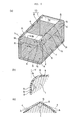
- FIG. 5(a) illustrates a perspective view of one example of the thermoelectric conversion device 10 according to the second embodiment of the present invention.
- the thermoelectric conversion device 10 has vertex portions M each formed by an outwardly convex curved surface g, and is almost in the shape of rectangular parallelepiped. These vertex portions M are in a state where each vertex A of the rectangular parallelepiped of the thermoelectric conversion device 10 in FIG. 2 is R-chamfered, i.e., chamfered by an outwardly convex curved surface such as a spherical surface.
- planes a and b, the planes a and c, and the planes b and c, surrounding the vertex portion M are connected via the curved surface g. At these connected portions, ridges Q are formed.
- FIG. 5(b) there is illustrated a partial cross-sectional view taken perpendicularly to the ridge Q along a dotted line Vb-Vb of the thermoelectric conversion device 10.
- an angle ⁇ created by the plane b and the curved surface g at the ridge Q is far greater than 90°, and is preferably about 180°C.
- the angle ⁇ created by the curved surface g and the plane b can be defined as the angle ⁇ created by: a tangent Z to the ridge Q of the curved surface g; and the plane b.
- FIG. 6(a) illustrates a perspective view of another example of a thermoelectric conversion device according to the second embodiment of the present invention.
- the thermoelectric conversion device 10 has ridge portions N each formed by an outwardly convex cylindrical curved surface h, and is almost in the shape of rectangular parallelepiped.
- the thermoelectric conversion device 10 in FIG. 6(a) is in a state where each ridge B of the thermoelectric conversion device 10 in FIG. 2 is R-chamfered, i.e., chamfered by a curved surface such as a cylindrical surface, and a new vertex T is formed instead of each vertex A.
- a ridge S is formed as a line along which the ridge portions N meet.
- the ridge portions N form the curved surfaces h each surrounded by: two ridges R parallel to the original ridge B; and the four ridges S.
- FIG. 6(b) there is illustrated a partial cross-sectional view taken perpendicularly to the axial direction of the ridge portion N along a dotted line VIb-VIb of the thermoelectric conversion device 10.
- two planes a and b are connected via the curved surface h by which the ridge portion N is formed.
- the cross-sectional shape of the ridge portion N is an outwardly convex curved surface, and is preferably a cylindrical surface. Accordingly, in a cross section taken perpendicularly to the ridge R, an angle ⁇ created by the plane b and the curved surface h at the ridge R is far greater than 90°, and is preferably about 180°.
- FIG. 6(c) there is illustrated a partial cross-sectional view taken perpendicularly to the ridge S along a dotted line VIc-VIc of the thermoelectric conversion device 10.
- the ridge S is a line along which the ridge portions N serving as the two curved surfaces are brought into contact with each other, and are gently connected.
- an angle ⁇ created by the curved surface h and the curved surface h at the ridge S is far greater than 90°, and is preferably about 180°.
- the angle ⁇ created by the curved surface h and the curved surface h can be defined as the angle ⁇ created by the tangents Z to the ridge S of the respective curved surfaces h.
- FIG. 7 (a) illustrates a perspective view of still another example of a thermoelectric conversion device according to the second embodiment of the present invention.
- the thermoelectric conversion device 10 is in a state where the vertexes T in FIG. 6 (a) are further R-chamfered, and the ridge portions N are connected via a vertex portion M that is an outwardly convex curved surface i, e.g., a spherical surface. At the connected portions, ridges U are formed.
- FIG. 7(b) there is illustrated a partial cross-sectional view taken perpendicularly to the ridge U along a dotted line VIIb-VIIb of the thermoelectric conversion device 10.
- the ridge U is a line along which the ridge portion N serving as the curved surface h and the vertex portion M serving as the curved surface i are brought into contact with each other. Accordingly, in a cross section taken perpendicularly to the ridge U, an angle ⁇ created by the curved surface h and the curved surface i at the ridge U is far greater than 90°, and is preferably about 180°.
- thermoelectric conversion device main body 1 and the film 8 materials for the thermoelectric conversion device main body 1 and the film 8, production methods thereof and the like are similar to those of the first embodiment.
- a method for R-chamfering the thermoelectric conversion device main body 1 a conventional processing method such as polishing using a rotary barrel or grinding may be used.
- thermoelectric conversion device main body 1 may have the ridge portions H and/or vertex portions G, which have been R-chamfered, the thermoelectric conversion device main body 1 may alternatively be produced without being chamfered.
- the numbers of the ridge portions N and vertex portions M are not limited, and the invention may be carried out even if right-angled or acute-angled ridges partially remain. From the viewpoint of resistance to characteristic degradation, it is preferable that a larger number of the ridge portions N and/or vertex portions M are provided and no right-angled or acute-angled ridge exists.
- the thermoelectric device main body 1 has the ridge portions N and/or vertex portions M at which the ridges B and/or vertexes A have been subjected to a chamfering process.
- the ridges Q, R, S and U have obtuse angles.
- the film can be easily formed to a uniform thickness similar to that of the other plane portion.
- thermoelectric conversion device 10 under a high temperature atmosphere, for example, even if an atmospheric gas is an oxidizing gas such as air by which the thermoelectric conversion device main body is likely to oxidize, or even if an atmospheric gas is a reducing gas such as an inert gas by which the reduction of the thermoelectric conversion device main body is likely to occur, the diffusion of the gas via the film is reduced, thus enabling the reduction of characteristic degradation in the thermoelectric conversion device.
- an atmospheric gas is an oxidizing gas such as air by which the thermoelectric conversion device main body is likely to oxidize
- a reducing gas such as an inert gas by which the reduction of the thermoelectric conversion device main body is likely to occur
- thermoelectric conversion module 20 in which thermoelectric conversion devices formed as described above are used, will be described with reference to FIG. 8 .
- a thermoelectric conversion module 20 mainly includes a substrate 15, p-type thermoelectric conversion devices 3, n-type thermoelectric conversion devices 4, electrodes 5, and input/output electrodes 6 and 7.
- thermoelectric conversion module 20 of the present embodiment a plurality of the p-type thermoelectric devices 3 and a plurality of the n-type thermoelectric devices 4 are provided over one surface la of the above-mentioned substrate 15 so that the longitudinal direction (y direction) of the plurality of p-type thermoelectric devices 3 and the plurality of n-type thermoelectric devices 4 extends along the widthwise direction (y direction) of the substrate 15 and the devices are separated from each other in the longitudinal direction (x direction) of the substrate 15.
- each of the thermoelectric conversion devices 3 and 4 is the thermoelectric conversion device 10 according to the first embodiment or the second embodiment.
- thermoelectric conversion module is capable of sufficiently reducing the degradation of thermoelectric conversion devices caused by oxidation or reduction even when the environment of usage is an oxidizing atmosphere or reducing atmosphere at high temperature.
- thermoelectric conversion devices have very low reactivity to oxidation or reduction, and thus can be suitably applied to a thermoelectric conversion module and the like operated in the high temperature air or in a corrosive gas atmosphere in particular.
- thermoelectric conversion device does not have to be formed into a rectangular parallelepiped shape, and may be formed into a disk-like shape or the like.
- thermoelectric conversion device main body was coated with a silica coating agent ("EPL-X-050" manufactured by Exousia Inc.) by dip-coating, and was subsequently fired in an air atmosphere at 300°C for 30 minutes to form a film of 0.5 ⁇ m, thus obtaining a thermoelectric conversion device.
- a silica coating agent (“EPL-X-050” manufactured by Exousia Inc.)
- thermoelectric conversion device was obtained similarly to Example 1 except that a film of 200 ⁇ m was formed by using a silica-alumina coating agent ("Betack#160CC” manufactured by Telnik Industrial Co. , Ltd.) as a coating agent, and performing firing at 200°C for one hour.
- a silica-alumina coating agent (“Betack#160CC” manufactured by Telnik Industrial Co. , Ltd.)
- thermoelectric conversion device was obtained similarly to Example 1 except that a film of 100 ⁇ m was formed by using a silica coating agent ("SPLW-Y” manufactured by Ceramic Coat Co., Ltd.) as a coating agent, and performing firing at 200°C for one hour.
- a silica coating agent (“SPLW-Y” manufactured by Ceramic Coat Co., Ltd.)
- thermoelectric conversion device was obtained similarly to Example 1 except that a film of 50 ⁇ m was formed by using a silicon carbide coating agent ("SPG26M” manufactured by Ceramic Coat Co., Ltd.) as a coating agent, and performing firing at 200°C for one hour.
- SPG26M silicon carbide coating agent manufactured by Ceramic Coat Co., Ltd.
- Thermoelectric conversion devices according to Comparative Examples 1 to 4 were obtained similarly to Examples 1 to 4, respectively, except that vertexes and ridges were not chamfered.
- thermoelectric conversion device according to Comparative Example 5 was obtained similarly to Example 1 except that no film was formed.
- thermoelectric conversion device according to Comparative Example 6 was obtained similarly to Comparative Example 1 except that no film was formed.
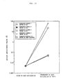
- thermoelectric conversion devices according to Examples 1 to 4 and Comparative Examples 1 to 6 For the respective thermoelectric conversion devices according to Examples 1 to 4 and Comparative Examples 1 to 6, measurements were made on initial resistance values in the room temperature air; then, the devices were heated and held at 700°C for two hours in the air, and the temperature was subsequently reduced to room temperature to make measurements on resistance values. As for the thermoelectric conversion device according to Example 1, a measurement was also made on a resistance value when the device was heated and held at 700°C for two hours in an inert atmosphere (nitrogen) and the temperature was subsequently reduced to room temperature.
- the measurements of the resistance values were made by attaching a four-terminal electrode using a silver paste after polishing and removing the film on two opposed planes using a sand paper.
- FIG. 9 illustrates resistance values of the chamfered thermoelectric conversion devices according to Examples 1 to 4 prior to and subsequent to heat application in the air; and resistance values of the thermoelectric conversion device according to Example 1 prior to and subsequent to heat application in an inert atmosphere.
- FIG. 10 illustrates resistance values of the thermoelectric conversion devices according to Comparative Examples 1 to 6 prior to and subsequent to heat application in the air.
- thermoelectric conversion devices according to Examples 1 to 4 were able to maintain the resistance values at sufficiently low levels even after the heat application in the air.
- Comparative Examples 1 to 6 the resistance values were considerably increased after the heat application in the air.
- thermoelectric conversion devices and production methods thereof which are capable of reducing the degradation of characteristics in a high temperature environment.
Landscapes
- Powder Metallurgy (AREA)
- Silicon Compounds (AREA)
Abstract
Description
- The present invention relates to thermoelectric conversion devices and production methods thereof.
- As thermoelectric conversion devices, a p-type thermoelectric conversion device made of a material such as Ca3CO4O9, NaxCoO2, CoSb3 or BiTeSb and an n-type thermoelectric conversion device made of a material such as SrTiO3, BaTiO3, Mg2Si or CaB6 have conventionally been known. Further, such thermoelectric conversion devices are often used at high temperature in an atmosphere such as air.
- Thermoelectric conversion characteristics of some thermoelectric conversion devices are degraded when subjected to high temperature.
- Therefore, an attempt has been made to cover the surface of a thermoelectric conversion device main body by a film of glass or the like (
JP 11-251647 - However, even with the foregoing method, it has been difficult to sufficiently maintain the characteristics of a thermoelectric conversion device. The present invention has been made in view of the above-described problems, and its object is to provide thermoelectric conversion devices and production methods thereof, which are capable of reducing the degradation of characteristics in a high temperature environment.
- After having conducted studies, the present inventor et al. found that: a thermoelectric conversion device main body has a ridge and a vertex, but it is difficult for a film to be sufficiently formed at this ridge or vertex; and the diffusion of an atmospheric gas from an outside atmosphere to a thermoelectric conversion device is likely to occur via the insufficient film at this ridge or vertex, which causes the degradation of the thermoelectric conversion device, and thus reached the concept of the present invention.
- A first thermoelectric conversion device according to the present invention is a thermoelectric conversion device including: a thermoelectric conversion device main body having a ridge portion and/or a vertex portion at which a ridge and/or a vertex have/has been subjected to a chamfering process; and a film covering a surface of the thermoelectric conversion device main body, including the ridge portion and/or the vertex portion thereof.
- Further, a second thermoelectric conversion device according to the present invention is a thermoelectric conversion device including: a thermoelectric conversion device main body having a ridge at which two faces meet, and having an angle created by the two faces at the ridge in a cross section taken perpendicularly to the ridge, the angle being an obtuse angle; and a film covering a surface of the thermoelectric conversion device main body, including the ridge.
- The first thermoelectric conversion device has the ridge portion and/or vertex portion at which the ridge and/or vertex have/has been subjected to a chamfering process. Accordingly, the film at the ridge portion and/or vertex portion can be easily formed to a thickness similar to that of the other portion.
- The second thermoelectric conversion device has an obtuse angle at the ridge, and therefore, the film at the ridge can be easily formed to a thickness similar to that of the other portion.
- Thus, even if an atmospheric gas, for example, is an oxidizing gas such as air in a high temperature atmosphere, by which the thermoelectric conversion device main body is likely to oxidize, the diffusion of the atmospheric gas is reduced due to the sufficient formation of the film, thereby enabling the reduction of characteristic degradation in the thermoelectric conversion device.
- In this aspect, the film of the thermoelectric conversion device is preferably an oxidation preventing film. Thus, even when subjected to high temperature in an oxidizing atmosphere such as air, the characteristics of the thermoelectric conversion device can be sufficiently maintained, thereby providing the thermoelectric conversion device having high general versatility.
- A main material for the film of the thermoelectric conversion device is preferably at least one of silica, alumina and silicon carbide. Thus, the thermoelectric conversion device having excellent oxidation resistance, heat resistance and abrasion resistance can be provided.
- The film of the thermoelectric conversion device preferably has a thickness of 0.01µm to 1mm, more preferably has a thickness of 0.1µm to 300µm, and even more preferably has a thickness of 1µm to 100µm. If the thickness of the film falls within the foregoing ranges, the diffusion of gas via the film during use at high temperature can be sufficiently reduced. Whereas if the thickness of the film is too small, there is a tendency to make it difficult to reduce the diffusion of gas, and if the thickness is too large, there is a tendency to facilitate occurrence of cracks in the film. Besides, the more uniform the thickness of the film, the better.
- A first method for producing a thermoelectric conversion device according to the present invention includes the steps of: performing a chamfering process on a ridge and/or a vertex of a thermoelectric conversion device main body; and forming a film on a surface of the thermoelectric conversion device main body, including a ridge portion and/or a vertex portion on which the chamfering process has been performed.
- A second method for producing a thermoelectric conversion device according to the present invention includes the steps of: preparing a thermoelectric conversion device main body having a ridge at which two faces meet, and having an angle created by the two faces at the ridge in a cross section taken perpendicularly to the ridge, the angle being an obtuse angle; and forming a film on a surface of the thermoelectric conversion device, including the ridge.
-
-
FIG. 1 shows a perspective view (a) of one example of a thermoelectric conversion device according to a first embodiment, and a partial cross-sectional view (b) taken perpendicularly to a ridge E along a dotted line IIb-IIb of thethermoelectric conversion device 10. -
FIG. 2 shows a perspective view of one example of a conventional thermoelectric conversion device main body. -
FIG. 3 shows a perspective view (a) of another example of a thermoelectric conversion device according to the first embodiment, a partial cross-sectional view (b) taken perpendicularly to the axial direction of a ridge portion H along a dotted line IIIb-IIIb of thethermoelectric conversion device 10, and a partial cross-sectional view (c) taken perpendicularly to a ridge F along a dotted line IIIc-IIIc of thethermoelectric conversion device 10. -
FIG. 4 shows a perspective view (a) of still another example of a thermoelectric conversion device according to the first embodiment, and a partial cross-sectional view (b) taken perpendicularly to a ridge K along a dotted line IVb-IVb of thethermoelectric conversion device 10. -
FIG. 5 shows a perspective view (a) of one example of a thermoelectric conversion device according to a second embodiment, and a partial cross-sectional view (b) taken perpendicularly to a ridge Q along a dotted line Vb-Vb of thethermoelectric conversion device 10. -
FIG. 6 shows a perspective view (a) of another example of a thermoelectric conversion device according to the second embodiment, a partial cross-sectional view (b) taken perpendicularly to the axial direction of a ridge portion N along a dotted line VIb-VIb of thethermoelectric conversion device 10, and a partial cross-sectional view (c) taken perpendicularly to a ridge S along a dotted line VIc-VIc of thethermoelectric conversion device 10. -
FIG. 7 shows a perspective view (a) of still another example of a thermoelectric conversion device according to the second embodiment, and a partial cross-sectional view (b) taken perpendicularly to a ridge U along a dotted line VIIb-VIIb of thethermoelectric conversion device 10. -
FIG. 8 shows one example of a thermoelectric conversion module. -
FIG. 9 shows resistance values of thermoelectric conversion devices according to Examples 1 to 4 prior to and subsequent to heat application in the air, and resistance values of the thermoelectric conversion device according to Example 1 prior to and subsequent to heat application in an inert atmosphere. -
FIG. 10 shows resistance values of thermoelectric conversion devices according to Comparative Examples 1 to 6 prior to and subsequent to heat application in the air. -
- 10
- thermoelectric conversion device
- 1
- thermoelectric conversion device main body
- 8
- film
- 1s
- exposed portion
- A, I, T
- vertex
- G, M
- vertex portion
- B, E, F, J, K, Q, R, S, U
- ridge
- H, N
- ridge portion
- a, b, c, d, e, f
- plane
- g, h, I
- curved surface
- Z
- tangent
- 20
- thermoelectric conversion module
- 15
- substrate
- 3
- p-type thermoelectric conversion device
- 4
- n-type thermoelectric conversion device
- 5
- electrode
- 6, 7
- input/output electrodes
- Hereinafter, preferred embodiments of the present invention will be illustrated in detail with reference to the appended drawings. In the description made with reference to the drawings, the same or equivalent elements are identified by the same reference characters, and redundant description thereof are not shown. Furthermore, dimensional ratios in the respective drawings are not necessarily identical to actual dimensional ratios.
-
FIG. 1(a) illustrates a perspective view of one example of a thermoelectric conversion device according to a first embodiment of the present invention. Thethermoelectric conversion device 10 has vertex portions G, and is almost in the shape of rectangular parallelepiped. Thethermoelectric conversion device 10 includes a thermoelectric conversion devicemain body 1, and afilm 8 that covers surfaces of the thermoelectric conversion devicemain body 1. Among the surfaces of the thermoelectric conversion devicemain body 1, one plane a (an upper face inFIG. 1(a) ) including the longest ridges B has an exposedportion 1s, at which the thermoelectric conversion devicemain body 1 is exposed, in respective given ranges from both longitudinal ends of this plane. When thethermoelectric conversion device 10 constitutes a thermoelectric conversion module, this exposedportion 1s is formed as an electrode connection portion for connecting a plurality of thethermoelectric conversion devices 10 in series. -
FIG. 2 illustrates a perspective view of one example of a conventional thermoelectric conversion device main body. The thermoelectric conversion devicemain body 1 is formed into a rectangular parallelepiped having a plurality of ridges B, and each vertex A is formed at a portion where the three ridges B meet. - The vertex portions G of the
thermoelectric conversion device 10 inFIG. 1(a) are in a state where each vertex A of the thermoelectric conversion devicemain body 1 inFIG. 2 is C-chamfered, i.e., in a state where each vertex is chamfered by a plane d. The vertex portions G in the C-chamfered state each form the plane d surrounded by three ridges E. - In
FIG. 1(b) , there is illustrated a partial cross-sectional view taken perpendicularly to the ridge E along a dotted line IIb-IIb of thethermoelectric conversion device 10. In a cross section taken perpendicularly to the ridge E, an angle α created by the two faces b and d, which form the ridge E, becomes an obtuse angle greater than 90° by C-chamfering. The angle α is preferably not less than 135°, and is more preferably not less than 157°. If the angle α is not more than 90° at this ridge E, thefilm 8 is not formed on the ridge E to a thickness equal to that of a plane portion around the ridge E. -
FIG. 3(a) illustrates a perspective view of another example of a thermoelectric conversion device according to the first embodiment of the present invention. Thethermoelectric conversion device 10 have C-chamfered ridge portions H, and is almost in the shape of rectangular parallelepiped. The ridge portions H of thethermoelectric conversion device 10 inFIG. 3(a) are in a state where each ridge B of thethermoelectric conversion device 10 inFIG. 2 is C-chamfered by a plane e. Instead of each vertex A, a new vertex I is formed at a point where the three ridge portions H meet. Around each vertex I, a ridge F is formed as a line along which the ridge portions H meet. The ridge portions H form the planes e each surrounded by: two ridges J parallel to the original ridge B, and the four ridges F. - In
FIG. 3(b) , there is illustrated a partial cross-sectional view taken perpendicularly to the axial direction of the ridge portion H along a dotted line IIIb-IIIb of thethermoelectric conversion device 10. In a cross section taken perpendicularly to the ridges J, angles β and β each created by the two planes, which form the ridge J, become obtuse angles greater than 90° by chamfering. The angles β and β' are each preferably similar to the angle α. If the angles β and β' are not more than 90°, thefilm 8 is not formed on the ridges J to a thickness equal to that of a plane portion around the ridges J. - In
FIG. 3(c ), there is illustrated a partial cross-sectional view taken perpendicularly to the ridge F along a dotted line IIIc-IIIc of thethermoelectric conversion device 10. In a cross section taken perpendicularly to the ridge F, an angle α created by the two faces, which form the ridge F, becomes an obtuse angle greater than 90° by chamfering. -
FIG. 4 (a) illustrates a perspective view of still another example of a thermoelectric conversion device according to the first embodiment of the present invention. Thethermoelectric conversion device 10 has vertex portions G and ridge portions H, and is usually formed into a rectangular parallelepiped. The thermoelectric conversion device inFIG. 4(a) is in a state where each vertex I of thethermoelectric conversion device 10 inFIG. 3 is further C-chamfered by a plane f, and the plane f of the vertex portion G becomes a plane surrounded by ridges K. - In
FIG. 4(b) , there is illustrated a partial cross-sectional view taken perpendicularly to the ridge K along a dotted line IVb-IVb of thethermoelectric conversion device 10. In a cross section taken perpendicularly to the ridge K, an angle α created by two faces e and f, which form the ridge K, becomes an obtuse angle greater than 90° by chamfering. - Examples of p-type thermoelectric device materials for the foregoing thermoelectric conversion device
main body 1 include metal composite oxides such as Ca3Co4O9 and NaxCoO2; silicides such as MnSi1.73, Fe1-xMnxSi2, Si0.8Ge0.2 and β-FeSi2; skutterudites such as CoSb3, FeSb3 and RFe3CoSb12 (where R represents La, Ce or Yb); and Te-containing alloys such as BiTeSb, PbTeSb, Bi2Te3 and PbTe. Furthermore, examples of n-type thermoelectric device materials include metal composite oxides such as SrTiO3, Zn1-xAlxO, CaMnO3, LaNiO3, BaxTi8O16, BaTiO3 and Ti1-xNbxO; silicides such as Mg2Si, Fe1-xCoxSi2, Si0.8Ge0.2 and β-FeSi2; skutterudites; clathrate compounds such as Ba8Al12Si30 and Ba8Al12Ge30; boron compounds such as CaB6, SrB6, BaB6 and CeB6; and Te-containing alloys such as BiTeSb, PbTeSb, Bi2Te3 and PbTe. - In particular, the present embodiment provides the
thermoelectric conversion device 10 including thefilm 8; therefore, for the thermoelectric conversion devicemain body 1, a material whose characteristics are likely to degrade due to oxidation in an oxidizing atmosphere or reduction in a non-oxidizing atmosphere within a high temperature environment can be suitably used. Examples of such materials include Zn4Sb3, CoSb3, Bi2Te3 and PbTe as materials for a p-type thermoelectric conversion device, and include SrTiO3, Zn1-xAlxO, BaTiO3, Bi2Te3 and PbTe as materials for an n-type thermoelectric device. - The
film 8 is preferably a film including, as a main material, one of silica, alumina and silicon carbide singly or a combination with another or more. Further, the thickness of thefilm 8 is preferably from 0.01µm to 1mm, more preferably from 0.1µm to 300µm, and even more preferably from 1µm to 100µm. If the thickness of thefilm 8 is too small, there is a tendency to make it difficult to reduce the diffusion of gas when thethermoelectric conversion device 10 is subjected to high temperature. On the other hand, if the upper limit of the thickness is too large, it becomes impossible to withstand thermal stress and the like since thefilm 8 is too thick, and there is a tendency to facilitate the occurrence of cracks. - In the foregoing thermoelectric conversion device, the thermoelectric device
main body 1 has the ridge portions H and/or vertex portions G at which the ridges B and/or vertexes A have been subjected to a chamfering process. In other words, the ridges E, F, J and K have obtuse angles. In particular, at the ridge portions H and/or vertex portions G, i.e., at the ridges E, F, J and/or K, in the foregoing thermoelectric conversion devicemain body 1, thefilm 8 can be easily formed to a uniform thickness similar to that of the other plane portion. - Accordingly, in the foregoing
thermoelectric conversion device 10 under a high temperature atmosphere, for example, even if an atmospheric gas is an oxidizing gas such as air by which the thermoelectric conversion device main body is likely to oxidize, or even if an atmospheric gas is a reducing gas such as an inert gas by which the reduction of the thermoelectric conversion device main body is likely to occur, the diffusion of the gas via the film is reduced, thus enabling the reduction of characteristic degradation in the thermoelectric conversion device. - In the present embodiment, the numbers of the ridge portions H and vertex portions G are not limited, and the invention may be carried out even if right-angled or acute-angled ridges partially remain. From the viewpoint of resistance to characteristic degradation, it is preferable that a larger number of the ridge portions H and/or vertex portions G are provided and no right-angled or acute-angled ridge exists.
- Next, a method for producing the foregoing thermoelectric conversion device will be briefly described.
- As a method for C-chamfering the thermoelectric conversion device
main body 1, a conventional method for processing a metal or ceramic material using a diamond cutter, a water-resistant paper, an abrasive cloth or the like may be used. - A method for forming the
film 8 is not particularly limited, and various methods such as sputtering and coating may be utilized. - In the sputtering, sputtering may be performed, for example, using a film material as a target.
- Furthermore, in the coating, a coating solution including a film precursor, for example, may be applied to the surface of the thermoelectric conversion device
main body 1, and then the film may be formed on the surface by performing processes such as drying, and firing. - As the coating solution, for example, a solution including a film precursor and a solvent for dissolving or dispersing this precursor may be used. As the film precursor, a silica precursor such as a silicon compound having a siloxane bond and/or polysilazane, an alumina precursor such as aluminum alkoxide, or a silicon carbide precursor such as polycarbosilane or polyvinylsilane may be used.
- As the solvent, for example, water and alcohols such as methanol and ethanol may be used, and one of these solvents may be used singly or a combination with another or more may be used.
- For the coating, spraying, dip-coating or the like may be used. Firing conditions require the firing to be performed at 200°C for one hour in the air, for example.
- A mask is formed in advance over the region of the exposed
portion 1s before the formation of the film, or part of the film is removed after the formation of thefilm 8, thereby allowing the exposedportion 1s to be formed as illustrated inFIG. 1 andFIGS. 3 and4 . - The thermoelectric conversion device
main body 1 may have the ridge portions H and/or vertex portions G which have been C-chamfered, or may alternatively have the foregoing form without being subjected to chamfering; for example, the thermoelectric conversion device main body may be produced without being chamfered by preparing a mold capable of forming the ridge portions H or vertex portions G which are in the chamfered state, by forming a green body including a thermoelectric conversion device material with the use of this mold, and then by using a method for firing the green body. - Next, thermoelectric devices according to a second embodiment will be described.
FIG. 5(a) illustrates a perspective view of one example of thethermoelectric conversion device 10 according to the second embodiment of the present invention. Thethermoelectric conversion device 10 has vertex portions M each formed by an outwardly convex curved surface g, and is almost in the shape of rectangular parallelepiped. These vertex portions M are in a state where each vertex A of the rectangular parallelepiped of thethermoelectric conversion device 10 inFIG. 2 is R-chamfered, i.e., chamfered by an outwardly convex curved surface such as a spherical surface. At each vertex portion M, planes a and b, the planes a and c, and the planes b and c, surrounding the vertex portion M, are connected via the curved surface g. At these connected portions, ridges Q are formed. - In
FIG. 5(b) , there is illustrated a partial cross-sectional view taken perpendicularly to the ridge Q along a dotted line Vb-Vb of thethermoelectric conversion device 10. In a cross section taken perpendicularly to the ridge Q, an angle α created by the plane b and the curved surface g at the ridge Q is far greater than 90°, and is preferably about 180°C. In this case, the angle α created by the curved surface g and the plane b can be defined as the angle α created by: a tangent Z to the ridge Q of the curved surface g; and the plane b. -
FIG. 6(a) illustrates a perspective view of another example of a thermoelectric conversion device according to the second embodiment of the present invention. Thethermoelectric conversion device 10 has ridge portions N each formed by an outwardly convex cylindrical curved surface h, and is almost in the shape of rectangular parallelepiped. Thethermoelectric conversion device 10 inFIG. 6(a) is in a state where each ridge B of thethermoelectric conversion device 10 inFIG. 2 is R-chamfered, i.e., chamfered by a curved surface such as a cylindrical surface, and a new vertex T is formed instead of each vertex A. Around each vertex T, a ridge S is formed as a line along which the ridge portions N meet. The ridge portions N form the curved surfaces h each surrounded by: two ridges R parallel to the original ridge B; and the four ridges S. - In
FIG. 6(b) , there is illustrated a partial cross-sectional view taken perpendicularly to the axial direction of the ridge portion N along a dotted line VIb-VIb of thethermoelectric conversion device 10. In a cross section taken perpendicularly to the axial direction of the ridge portion N, two planes a and b are connected via the curved surface h by which the ridge portion N is formed. The cross-sectional shape of the ridge portion N is an outwardly convex curved surface, and is preferably a cylindrical surface. Accordingly, in a cross section taken perpendicularly to the ridge R, an angle β created by the plane b and the curved surface h at the ridge R is far greater than 90°, and is preferably about 180°. - Furthermore, in
FIG. 6(c) , there is illustrated a partial cross-sectional view taken perpendicularly to the ridge S along a dotted line VIc-VIc of thethermoelectric conversion device 10. The ridge S is a line along which the ridge portions N serving as the two curved surfaces are brought into contact with each other, and are gently connected. Accordingly, in a cross section taken perpendicularly to the ridge S, an angle α created by the curved surface h and the curved surface h at the ridge S is far greater than 90°, and is preferably about 180°. In this case, the angle α created by the curved surface h and the curved surface h can be defined as the angle α created by the tangents Z to the ridge S of the respective curved surfaces h. -
FIG. 7 (a) illustrates a perspective view of still another example of a thermoelectric conversion device according to the second embodiment of the present invention. Thethermoelectric conversion device 10 is in a state where the vertexes T inFIG. 6 (a) are further R-chamfered, and the ridge portions N are connected via a vertex portion M that is an outwardly convex curved surface i, e.g., a spherical surface. At the connected portions, ridges U are formed. - In
FIG. 7(b) , there is illustrated a partial cross-sectional view taken perpendicularly to the ridge U along a dotted line VIIb-VIIb of thethermoelectric conversion device 10. The ridge U is a line along which the ridge portion N serving as the curved surface h and the vertex portion M serving as the curved surface i are brought into contact with each other. Accordingly, in a cross section taken perpendicularly to the ridge U, an angle α created by the curved surface h and the curved surface i at the ridge U is far greater than 90°, and is preferably about 180°. - As for the second embodiment according to the present invention, materials for the thermoelectric conversion device
main body 1 and thefilm 8, production methods thereof and the like are similar to those of the first embodiment. In particular, as a method for R-chamfering the thermoelectric conversion devicemain body 1, a conventional processing method such as polishing using a rotary barrel or grinding may be used. - Moreover, the second embodiment is similar to the first embodiment in that although the thermoelectric conversion device
main body 1 may have the ridge portions H and/or vertex portions G, which have been R-chamfered, the thermoelectric conversion devicemain body 1 may alternatively be produced without being chamfered. - Besides, in the present embodiment, the numbers of the ridge portions N and vertex portions M are not limited, and the invention may be carried out even if right-angled or acute-angled ridges partially remain. From the viewpoint of resistance to characteristic degradation, it is preferable that a larger number of the ridge portions N and/or vertex portions M are provided and no right-angled or acute-angled ridge exists.
- In the foregoing thermoelectric conversion device, the thermoelectric device
main body 1 has the ridge portions N and/or vertex portions M at which the ridges B and/or vertexes A have been subjected to a chamfering process. In other words, the ridges Q, R, S and U have obtuse angles. In particular, at the ridge portions N and/or vertex portions M, i.e., at the ridges Q, R, S and/or U, in the foregoing thermoelectric conversion devicemain body 1, the film can be easily formed to a uniform thickness similar to that of the other plane portion. - Accordingly, in the foregoing
thermoelectric conversion device 10 under a high temperature atmosphere, for example, even if an atmospheric gas is an oxidizing gas such as air by which the thermoelectric conversion device main body is likely to oxidize, or even if an atmospheric gas is a reducing gas such as an inert gas by which the reduction of the thermoelectric conversion device main body is likely to occur, the diffusion of the gas via the film is reduced, thus enabling the reduction of characteristic degradation in the thermoelectric conversion device. - A thermoelectric conversion module, in which thermoelectric conversion devices formed as described above are used, will be described with reference to
FIG. 8 . Athermoelectric conversion module 20 mainly includes asubstrate 15, p-typethermoelectric conversion devices 3, n-typethermoelectric conversion devices 4,electrodes 5, and input/output electrodes 6 and 7. Specifically, in thethermoelectric conversion module 20 of the present embodiment, a plurality of the p-typethermoelectric devices 3 and a plurality of the n-typethermoelectric devices 4 are provided over one surface la of the above-mentionedsubstrate 15 so that the longitudinal direction (y direction) of the plurality of p-typethermoelectric devices 3 and the plurality of n-typethermoelectric devices 4 extends along the widthwise direction (y direction) of thesubstrate 15 and the devices are separated from each other in the longitudinal direction (x direction) of thesubstrate 15. Further, each of thethermoelectric conversion devices thermoelectric conversion device 10 according to the first embodiment or the second embodiment. - The foregoing thermoelectric conversion module is capable of sufficiently reducing the degradation of thermoelectric conversion devices caused by oxidation or reduction even when the environment of usage is an oxidizing atmosphere or reducing atmosphere at high temperature.
- Especially the thermoelectric conversion devices have very low reactivity to oxidation or reduction, and thus can be suitably applied to a thermoelectric conversion module and the like operated in the high temperature air or in a corrosive gas atmosphere in particular.
- The present invention is not limited to the above-described embodiments, and various modified forms may be provided. For example, there may be provided a form in which a ridge portion and a vertex portion, which are in C-chamfered states, are combined with a ridge portion and a vertex portion, which are in R-chamfered states. Furthermore, the thermoelectric conversion device does not have to be formed into a rectangular parallelepiped shape, and may be formed into a disk-like shape or the like.
- Examples and comparative examples in the present invention will be specifically described, but the present invention is not limited to these examples.
- A sintered body of a titania-based thermoelectric material (NbxTii-xO3, where X=0.5) was prepared, and a cube of 4 mm per side was cut out with a diamond cutter, thereby providing a thermoelectric conversion device main body. Subsequently, all vertexes and ridges of this cube were R-chamfered using a sand paper, thus performing an operation for removing sharp edges.
- Then, the chamfered thermoelectric conversion device main body was coated with a silica coating agent ("EPL-X-050" manufactured by Exousia Inc.) by dip-coating, and was subsequently fired in an air atmosphere at 300°C for 30 minutes to form a film of 0.5µm, thus obtaining a thermoelectric conversion device.
- A thermoelectric conversion device was obtained similarly to Example 1 except that a film of 200µm was formed by using a silica-alumina coating agent ("Betack#160CC" manufactured by Telnik Industrial Co. , Ltd.) as a coating agent, and performing firing at 200°C for one hour.
- A thermoelectric conversion device was obtained similarly to Example 1 except that a film of 100µm was formed by using a silica coating agent ("SPLW-Y" manufactured by Ceramic Coat Co., Ltd.) as a coating agent, and performing firing at 200°C for one hour.
- A thermoelectric conversion device was obtained similarly to Example 1 except that a film of 50µm was formed by using a silicon carbide coating agent ("SPG26M" manufactured by Ceramic Coat Co., Ltd.) as a coating agent, and performing firing at 200°C for one hour.
- Thermoelectric conversion devices according to Comparative Examples 1 to 4 were obtained similarly to Examples 1 to 4, respectively, except that vertexes and ridges were not chamfered.
- A thermoelectric conversion device according to Comparative Example 5 was obtained similarly to Example 1 except that no film was formed.
- A thermoelectric conversion device according to Comparative Example 6 was obtained similarly to Comparative Example 1 except that no film was formed.
- For the respective thermoelectric conversion devices according to Examples 1 to 4 and Comparative Examples 1 to 6, measurements were made on initial resistance values in the room temperature air; then, the devices were heated and held at 700°C for two hours in the air, and the temperature was subsequently reduced to room temperature to make measurements on resistance values. As for the thermoelectric conversion device according to Example 1, a measurement was also made on a resistance value when the device was heated and held at 700°C for two hours in an inert atmosphere (nitrogen) and the temperature was subsequently reduced to room temperature.
- The measurements of the resistance values were made by attaching a four-terminal electrode using a silver paste after polishing and removing the film on two opposed planes using a sand paper.
-
FIG. 9 illustrates resistance values of the chamfered thermoelectric conversion devices according to Examples 1 to 4 prior to and subsequent to heat application in the air; and resistance values of the thermoelectric conversion device according to Example 1 prior to and subsequent to heat application in an inert atmosphere. Furthermore,FIG. 10 illustrates resistance values of the thermoelectric conversion devices according to Comparative Examples 1 to 6 prior to and subsequent to heat application in the air. - The thermoelectric conversion devices according to Examples 1 to 4 were able to maintain the resistance values at sufficiently low levels even after the heat application in the air. On the other hand, in Comparative Examples 1 to 6, the resistance values were considerably increased after the heat application in the air.
- According to the present invention, there are provided thermoelectric conversion devices and production methods thereof, which are capable of reducing the degradation of characteristics in a high temperature environment.
Claims (8)
- A thermoelectric conversion device comprising:a thermoelectric conversion device main body having a ridge portion and/or a vertex portion at which a ridge and/or a vertex have/has been subjected to a chamfering process; anda film covering a surface of the thermoelectric conversion device main body, including the ridge portion and/or the vertex portion thereof.
- A thermoelectric conversion device comprising:a thermoelectric conversion device main body having a ridge at which two faces meet, and having an angle created by the two faces at the ridge in a cross section taken perpendicularly to the ridge, the angle being an obtuse angle; anda film covering a surface of the thermoelectric conversion device main body, including the ridge.
- The thermoelectric conversion device according to either claim 1 or 2, wherein the film is an oxidation preventing film.
- The thermoelectric conversion device according to any one of claims 1 to 3, wherein a main material for the film is at least one of silica, alumina and silicon carbide.
- The thermoelectric conversion device according to any one of claims 1 to 4, wherein the film has a thickness of 0.01µm to 1mm.
- The thermoelectric conversion device according to any one of claims 1 to 4, wherein the film has a thickness of 0.1µm to 300µm.
- A method for producing a thermoelectric conversion device, comprising the steps of:performing a chamfering process on a ridge and/or a vertex of a thermoelectric conversion device main body; andforming a film on a surface of the thermoelectric conversion device main body, including a ridge portion and/or a vertex portion on which the chamfering process has been performed.
- A method for producing a thermoelectric conversion device, comprising the steps of:preparing a thermoelectric conversion device main body having a ridge at which two faces meet, and having an angle created by the two faces at the ridge in a cross section taken perpendicularly to the ridge, the angle being an obtuse angle; andforming a film on a surface of the thermoelectric conversion device, including the ridge.
Applications Claiming Priority (2)
| Application Number | Priority Date | Filing Date | Title |
|---|---|---|---|
| JP2007195109A JP4912975B2 (en) | 2007-07-26 | 2007-07-26 | Thermoelectric conversion element and manufacturing method thereof |
| PCT/JP2008/063484 WO2009014243A1 (en) | 2007-07-26 | 2008-07-22 | Thermoelectric conversion element and method for manufacturing the same |
Publications (2)
| Publication Number | Publication Date |
|---|---|
| EP2187460A1 true EP2187460A1 (en) | 2010-05-19 |
| EP2187460A4 EP2187460A4 (en) | 2012-01-18 |
Family
ID=40281484
Family Applications (1)
| Application Number | Title | Priority Date | Filing Date |
|---|---|---|---|
| EP08791720A Withdrawn EP2187460A4 (en) | 2007-07-26 | 2008-07-22 | THERMOELECTRIC CONVERSION ELEMENT AND METHOD OF MANUFACTURE |
Country Status (6)
| Country | Link |
|---|---|
| US (1) | US20100193004A1 (en) |
| EP (1) | EP2187460A4 (en) |
| JP (1) | JP4912975B2 (en) |
| CN (1) | CN101755349A (en) |
| TW (1) | TW200913332A (en) |
| WO (1) | WO2009014243A1 (en) |
Families Citing this family (7)
| Publication number | Priority date | Publication date | Assignee | Title |
|---|---|---|---|---|
| JP6152262B2 (en) * | 2012-11-28 | 2017-06-21 | 株式会社フジコー | Thermoelectric conversion device and manufacturing method thereof |
| JP5920537B2 (en) * | 2013-08-09 | 2016-05-18 | 株式会社村田製作所 | Multilayer thermoelectric conversion element |
| JP6112217B2 (en) * | 2013-10-11 | 2017-04-12 | 株式会社村田製作所 | Multilayer thermoelectric conversion element |
| KR20170089329A (en) * | 2016-01-26 | 2017-08-03 | 현대자동차주식회사 | Thermoelectric element and thermoelectric module having the same |
| JP2018046275A (en) * | 2016-09-08 | 2018-03-22 | 国立研究開発法人産業技術総合研究所 | Thermoelectric power generation device and manufacturing method thereof |
| CN107180909B (en) * | 2017-07-05 | 2019-05-03 | 东北大学 | Thermoelectric arms of inclined polyhedron structure |
| WO2026094629A1 (en) * | 2024-10-31 | 2026-05-07 | パナソニックIpマネジメント株式会社 | Thermoelectric conversion element, thermoelectric conversion structure, thermoelectric conversion module, thermoelectric conversion system, and temperature control system |
Family Cites Families (10)
| Publication number | Priority date | Publication date | Assignee | Title |
|---|---|---|---|---|
| US3617376A (en) * | 1967-03-16 | 1971-11-02 | North American Rockwell | Antisublimation coating and method for thermoelectric materials |
| US5356484A (en) * | 1992-03-30 | 1994-10-18 | Yater Joseph C | Reversible thermoelectric converter |
| JPH09186368A (en) * | 1995-10-31 | 1997-07-15 | Technova:Kk | Thick film thermoelectric element |
| JPH11177151A (en) * | 1997-12-08 | 1999-07-02 | Yamaha Corp | Thermoelectric module |
| JPH11251647A (en) * | 1998-02-27 | 1999-09-17 | Ueki Corporation:Kk | Thermoelectric conversion element, thermoelectric conversion device, and method of manufacturing these |
| US6700053B2 (en) * | 2000-07-03 | 2004-03-02 | Komatsu Ltd. | Thermoelectric module |
| JP2005302783A (en) * | 2004-04-06 | 2005-10-27 | Toshiba Corp | Thermoelectric conversion module, shape evaluation apparatus and shape evaluation method thereof |
| WO2006011581A1 (en) * | 2004-07-27 | 2006-02-02 | Sumitomo Chemical Company, Limited | Thermoelectric conversion material and process for producing the same |
| JP2006100683A (en) * | 2004-09-30 | 2006-04-13 | Sumitomo Chemical Co Ltd | Titanium oxide thermoelectric conversion material |
| JP2006066460A (en) * | 2004-08-24 | 2006-03-09 | Komatsu Ltd | Thermoelectric element |
-
2007
- 2007-07-26 JP JP2007195109A patent/JP4912975B2/en not_active Expired - Fee Related
-
2008
- 2008-07-22 EP EP08791720A patent/EP2187460A4/en not_active Withdrawn
- 2008-07-22 CN CN200880100052A patent/CN101755349A/en active Pending
- 2008-07-22 TW TW097127749A patent/TW200913332A/en unknown
- 2008-07-22 US US12/669,654 patent/US20100193004A1/en not_active Abandoned
- 2008-07-22 WO PCT/JP2008/063484 patent/WO2009014243A1/en not_active Ceased
Also Published As
| Publication number | Publication date |
|---|---|
| EP2187460A4 (en) | 2012-01-18 |
| US20100193004A1 (en) | 2010-08-05 |
| JP4912975B2 (en) | 2012-04-11 |
| JP2009032893A (en) | 2009-02-12 |
| WO2009014243A1 (en) | 2009-01-29 |
| TW200913332A (en) | 2009-03-16 |
| CN101755349A (en) | 2010-06-23 |
Similar Documents
| Publication | Publication Date | Title |
|---|---|---|
| US20100193004A1 (en) | Thermoelectric conversion element and method for manufacturing the same | |
| EP2088634A1 (en) | Thermo-electric converting material, process for producing the same, thermo-electric converting element, and method of heightening strength of thermo-electric converting material | |
| EP2460182B1 (en) | A coating for thermoelectric materials and a device containing the same | |
| EP2415089B1 (en) | Thermoelectric material coated with a protective layer | |
| US8390113B2 (en) | Thermoelectric conversion module | |
| US20120145214A1 (en) | Thermoelectric conversion material, and thermoelectric conversion module using same | |
| US20110298080A1 (en) | Method for manufacturing thermoelectric conversion module, and thermoelectric conversion module | |
| EP3651217A1 (en) | Thermoelectric conversion module and method for producing thermoelectric conversion module | |
| JP2008305991A (en) | Thermoelectric conversion module, thermoelectric conversion device, and manufacturing method thereof | |
| JP4668233B2 (en) | Thermoelectric conversion element, thermoelectric conversion module, and method of manufacturing thermoelectric conversion module | |
| US20130200989A1 (en) | Semiconductor ceramic element and method for producing same | |
| JP6966666B2 (en) | Manufacturing method of temperature sensor element and temperature sensor element | |
| EP3315476A1 (en) | Ceramic substrate and mounting substrate using same, and electronic device | |
| WO2016153073A1 (en) | Nitride thermoelectric conversion material and manufacturing method therefor and thermoelectric conversion element | |
| EP2937441A1 (en) | Metal-nitride thermistor material, manufacturing method therefor, and film-type thermistor sensor | |
| US20100031993A1 (en) | Thermoelectric conversion material and thermoelectric conversion device | |
| CN104321889B (en) | Thermo-electric converting material and use its thermo-electric conversion module and its manufacture method | |
| WO2015012414A1 (en) | Metal nitride material for thermistor, production method for same, and film-type thermistor sensor | |
| JP7021872B2 (en) | Composite thermoelectric material and its manufacturing method | |
| CN101558504A (en) | Thermo-electric converting material, process for producing the same, thermo-electric converting element, and method of heightening strength of thermo-electric converting material | |
| TWI752242B (en) | Thermoelectric conversion module and method for producing thermoelectric conversion module | |
| JP5218285B2 (en) | Thermoelectric conversion material | |
| KR20050048601A (en) | Aluminum nitride sintered compact, metallized substrate, heater,jig and method for producing aluminum nitride sintered compact | |
| CN119923697A (en) | Thermistor element and method for manufacturing the same | |
| JP2007096205A (en) | Chip-type negative temperature coefficient (ntc) element |
Legal Events
| Date | Code | Title | Description |
|---|---|---|---|
| PUAI | Public reference made under article 153(3) epc to a published international application that has entered the european phase |
Free format text: ORIGINAL CODE: 0009012 |
|
| 17P | Request for examination filed |
Effective date: 20100224 |
|
| AK | Designated contracting states |
Kind code of ref document: A1 Designated state(s): AT BE BG CH CY CZ DE DK EE ES FI FR GB GR HR HU IE IS IT LI LT LU LV MC MT NL NO PL PT RO SE SI SK TR |
|
| AX | Request for extension of the european patent |
Extension state: AL BA MK RS |
|
| DAX | Request for extension of the european patent (deleted) | ||
| A4 | Supplementary search report drawn up and despatched |
Effective date: 20111219 |
|
| RIC1 | Information provided on ipc code assigned before grant |
Ipc: H01L 35/34 20060101ALI20111213BHEP Ipc: H01L 35/32 20060101AFI20111213BHEP |
|
| STAA | Information on the status of an ep patent application or granted ep patent |
Free format text: STATUS: THE APPLICATION IS DEEMED TO BE WITHDRAWN |
|
| 18D | Application deemed to be withdrawn |
Effective date: 20120717 |