EP2184775A1 - Semiconductor device, and its manufacturing method - Google Patents
Semiconductor device, and its manufacturing method Download PDFInfo
- Publication number
- EP2184775A1 EP2184775A1 EP08792454A EP08792454A EP2184775A1 EP 2184775 A1 EP2184775 A1 EP 2184775A1 EP 08792454 A EP08792454 A EP 08792454A EP 08792454 A EP08792454 A EP 08792454A EP 2184775 A1 EP2184775 A1 EP 2184775A1
- Authority
- EP
- European Patent Office
- Prior art keywords
- insulating film
- semiconductor device
- interlayer insulating
- forming
- sio
- Prior art date
- Legal status (The legal status is an assumption and is not a legal conclusion. Google has not performed a legal analysis and makes no representation as to the accuracy of the status listed.)
- Withdrawn
Links
Images






Classifications
-
- H—ELECTRICITY
- H10—SEMICONDUCTOR DEVICES; ELECTRIC SOLID-STATE DEVICES NOT OTHERWISE PROVIDED FOR
- H10P—GENERIC PROCESSES OR APPARATUS FOR THE MANUFACTURE OR TREATMENT OF DEVICES COVERED BY CLASS H10
- H10P14/00—Formation of materials, e.g. in the shape of layers or pillars
- H10P14/60—Formation of materials, e.g. in the shape of layers or pillars of insulating materials
- H10P14/63—Formation of materials, e.g. in the shape of layers or pillars of insulating materials characterised by the formation processes
- H10P14/6302—Non-deposition formation processes
- H10P14/6322—Formation by thermal treatments
-
- H—ELECTRICITY
- H10—SEMICONDUCTOR DEVICES; ELECTRIC SOLID-STATE DEVICES NOT OTHERWISE PROVIDED FOR
- H10D—INORGANIC ELECTRIC SEMICONDUCTOR DEVICES
- H10D84/00—Integrated devices formed in or on semiconductor substrates that comprise only semiconducting layers, e.g. on Si wafers or on GaAs-on-Si wafers
- H10D84/01—Manufacture or treatment
- H10D84/0123—Integrating together multiple components covered by H10D12/00 or H10D30/00, e.g. integrating multiple IGBTs
- H10D84/0126—Integrating together multiple components covered by H10D12/00 or H10D30/00, e.g. integrating multiple IGBTs the components including insulated gates, e.g. IGFETs
- H10D84/0151—Manufacturing their isolation regions
-
- H—ELECTRICITY
- H10—SEMICONDUCTOR DEVICES; ELECTRIC SOLID-STATE DEVICES NOT OTHERWISE PROVIDED FOR
- H10P—GENERIC PROCESSES OR APPARATUS FOR THE MANUFACTURE OR TREATMENT OF DEVICES COVERED BY CLASS H10
- H10P14/00—Formation of materials, e.g. in the shape of layers or pillars
- H10P14/60—Formation of materials, e.g. in the shape of layers or pillars of insulating materials
- H10P14/66—Formation of materials, e.g. in the shape of layers or pillars of insulating materials characterised by the type of materials
- H10P14/662—Laminate layers, e.g. stacks of alternating high-k metal oxides
-
- H—ELECTRICITY
- H10—SEMICONDUCTOR DEVICES; ELECTRIC SOLID-STATE DEVICES NOT OTHERWISE PROVIDED FOR
- H10P—GENERIC PROCESSES OR APPARATUS FOR THE MANUFACTURE OR TREATMENT OF DEVICES COVERED BY CLASS H10
- H10P14/00—Formation of materials, e.g. in the shape of layers or pillars
- H10P14/60—Formation of materials, e.g. in the shape of layers or pillars of insulating materials
- H10P14/68—Organic materials, e.g. photoresists
- H10P14/683—Organic materials, e.g. photoresists carbon-based polymeric organic materials, e.g. polyimides, poly cyclobutene or PVC
-
- H—ELECTRICITY
- H10—SEMICONDUCTOR DEVICES; ELECTRIC SOLID-STATE DEVICES NOT OTHERWISE PROVIDED FOR
- H10P—GENERIC PROCESSES OR APPARATUS FOR THE MANUFACTURE OR TREATMENT OF DEVICES COVERED BY CLASS H10
- H10P95/00—Generic processes or apparatus for manufacture or treatments not covered by the other groups of this subclass
- H10P95/90—Thermal treatments, e.g. annealing or sintering
-
- H—ELECTRICITY
- H10—SEMICONDUCTOR DEVICES; ELECTRIC SOLID-STATE DEVICES NOT OTHERWISE PROVIDED FOR
- H10W—GENERIC PACKAGES, INTERCONNECTIONS, CONNECTORS OR OTHER CONSTRUCTIONAL DETAILS OF DEVICES COVERED BY CLASS H10
- H10W10/00—Isolation regions in semiconductor bodies between components of integrated devices
- H10W10/01—Manufacture or treatment
- H10W10/011—Manufacture or treatment of isolation regions comprising dielectric materials
- H10W10/012—Manufacture or treatment of isolation regions comprising dielectric materials using local oxidation of silicon [LOCOS]
- H10W10/0121—Manufacture or treatment of isolation regions comprising dielectric materials using local oxidation of silicon [LOCOS] in regions recessed from the surface, e.g. in trenches or grooves
-
- H—ELECTRICITY
- H10—SEMICONDUCTOR DEVICES; ELECTRIC SOLID-STATE DEVICES NOT OTHERWISE PROVIDED FOR
- H10W—GENERIC PACKAGES, INTERCONNECTIONS, CONNECTORS OR OTHER CONSTRUCTIONAL DETAILS OF DEVICES COVERED BY CLASS H10
- H10W20/00—Interconnections in chips, wafers or substrates
- H10W20/01—Manufacture or treatment
- H10W20/031—Manufacture or treatment of conductive parts of the interconnections
- H10W20/069—Manufacture or treatment of conductive parts of the interconnections by forming self-aligned vias or self-aligned contact plugs
-
- H—ELECTRICITY
- H10—SEMICONDUCTOR DEVICES; ELECTRIC SOLID-STATE DEVICES NOT OTHERWISE PROVIDED FOR
- H10W—GENERIC PACKAGES, INTERCONNECTIONS, CONNECTORS OR OTHER CONSTRUCTIONAL DETAILS OF DEVICES COVERED BY CLASS H10
- H10W20/00—Interconnections in chips, wafers or substrates
- H10W20/01—Manufacture or treatment
- H10W20/071—Manufacture or treatment of dielectric parts thereof
-
- H—ELECTRICITY
- H10—SEMICONDUCTOR DEVICES; ELECTRIC SOLID-STATE DEVICES NOT OTHERWISE PROVIDED FOR
- H10W—GENERIC PACKAGES, INTERCONNECTIONS, CONNECTORS OR OTHER CONSTRUCTIONAL DETAILS OF DEVICES COVERED BY CLASS H10
- H10W20/00—Interconnections in chips, wafers or substrates
- H10W20/01—Manufacture or treatment
- H10W20/071—Manufacture or treatment of dielectric parts thereof
- H10W20/081—Manufacture or treatment of dielectric parts thereof by forming openings in the dielectric parts
- H10W20/084—Manufacture or treatment of dielectric parts thereof by forming openings in the dielectric parts for dual-damascene structures
-
- H—ELECTRICITY
- H10—SEMICONDUCTOR DEVICES; ELECTRIC SOLID-STATE DEVICES NOT OTHERWISE PROVIDED FOR
- H10W—GENERIC PACKAGES, INTERCONNECTIONS, CONNECTORS OR OTHER CONSTRUCTIONAL DETAILS OF DEVICES COVERED BY CLASS H10
- H10W20/00—Interconnections in chips, wafers or substrates
- H10W20/01—Manufacture or treatment
- H10W20/071—Manufacture or treatment of dielectric parts thereof
- H10W20/093—Manufacture or treatment of dielectric parts thereof by modifying materials of the dielectric parts
- H10W20/097—Manufacture or treatment of dielectric parts thereof by modifying materials of the dielectric parts by thermally treating
-
- H—ELECTRICITY
- H10—SEMICONDUCTOR DEVICES; ELECTRIC SOLID-STATE DEVICES NOT OTHERWISE PROVIDED FOR
- H10W—GENERIC PACKAGES, INTERCONNECTIONS, CONNECTORS OR OTHER CONSTRUCTIONAL DETAILS OF DEVICES COVERED BY CLASS H10
- H10W20/00—Interconnections in chips, wafers or substrates
- H10W20/40—Interconnections external to wafers or substrates, e.g. back-end-of-line [BEOL] metallisations or vias connecting to gate electrodes
- H10W20/45—Interconnections external to wafers or substrates, e.g. back-end-of-line [BEOL] metallisations or vias connecting to gate electrodes characterised by their insulating parts
- H10W20/47—Interconnections external to wafers or substrates, e.g. back-end-of-line [BEOL] metallisations or vias connecting to gate electrodes characterised by their insulating parts comprising two or more dielectric layers having different properties, e.g. different dielectric constants
-
- H—ELECTRICITY
- H10—SEMICONDUCTOR DEVICES; ELECTRIC SOLID-STATE DEVICES NOT OTHERWISE PROVIDED FOR
- H10W—GENERIC PACKAGES, INTERCONNECTIONS, CONNECTORS OR OTHER CONSTRUCTIONAL DETAILS OF DEVICES COVERED BY CLASS H10
- H10W42/00—Arrangements for protection of devices
- H10W42/20—Arrangements for protection of devices protecting against electromagnetic or particle radiation, e.g. light, X-rays, gamma-rays or electrons
- H10W42/261—Arrangements for protection of devices protecting against electromagnetic or particle radiation, e.g. light, X-rays, gamma-rays or electrons characterised by their shapes or dispositions
- H10W42/276—Arrangements for protection of devices protecting against electromagnetic or particle radiation, e.g. light, X-rays, gamma-rays or electrons characterised by their shapes or dispositions the arrangements being on an external surface of the package, e.g. on the outer surface of an encapsulation
-
- H—ELECTRICITY
- H10—SEMICONDUCTOR DEVICES; ELECTRIC SOLID-STATE DEVICES NOT OTHERWISE PROVIDED FOR
- H10W—GENERIC PACKAGES, INTERCONNECTIONS, CONNECTORS OR OTHER CONSTRUCTIONAL DETAILS OF DEVICES COVERED BY CLASS H10
- H10W70/00—Package substrates; Interposers; Redistribution layers [RDL]
- H10W70/01—Manufacture or treatment
- H10W70/05—Manufacture or treatment of insulating or insulated package substrates, or of interposers, or of redistribution layers
- H10W70/08—Manufacture or treatment of insulating or insulated package substrates, or of interposers, or of redistribution layers by depositing layers on the chip or wafer, e.g. "chip-first" RDLs
- H10W70/09—Manufacture or treatment of insulating or insulated package substrates, or of interposers, or of redistribution layers by depositing layers on the chip or wafer, e.g. "chip-first" RDLs extending onto an encapsulation that laterally surrounds the chip or wafer, e.g. fan-out wafer level package [FOWLP] RDLs
-
- H—ELECTRICITY
- H10—SEMICONDUCTOR DEVICES; ELECTRIC SOLID-STATE DEVICES NOT OTHERWISE PROVIDED FOR
- H10W—GENERIC PACKAGES, INTERCONNECTIONS, CONNECTORS OR OTHER CONSTRUCTIONAL DETAILS OF DEVICES COVERED BY CLASS H10
- H10W72/00—Interconnections or connectors in packages
- H10W72/01—Manufacture or treatment
- H10W72/0198—Manufacture or treatment batch processes
-
- H—ELECTRICITY
- H10—SEMICONDUCTOR DEVICES; ELECTRIC SOLID-STATE DEVICES NOT OTHERWISE PROVIDED FOR
- H10D—INORGANIC ELECTRIC SEMICONDUCTOR DEVICES
- H10D84/00—Integrated devices formed in or on semiconductor substrates that comprise only semiconducting layers, e.g. on Si wafers or on GaAs-on-Si wafers
- H10D84/01—Manufacture or treatment
- H10D84/0123—Integrating together multiple components covered by H10D12/00 or H10D30/00, e.g. integrating multiple IGBTs
- H10D84/0126—Integrating together multiple components covered by H10D12/00 or H10D30/00, e.g. integrating multiple IGBTs the components including insulated gates, e.g. IGFETs
- H10D84/013—Manufacturing their source or drain regions, e.g. silicided source or drain regions
- H10D84/0133—Manufacturing common source or drain regions between multiple IGFETs
-
- H—ELECTRICITY
- H10—SEMICONDUCTOR DEVICES; ELECTRIC SOLID-STATE DEVICES NOT OTHERWISE PROVIDED FOR
- H10D—INORGANIC ELECTRIC SEMICONDUCTOR DEVICES
- H10D84/00—Integrated devices formed in or on semiconductor substrates that comprise only semiconducting layers, e.g. on Si wafers or on GaAs-on-Si wafers
- H10D84/01—Manufacture or treatment
- H10D84/0123—Integrating together multiple components covered by H10D12/00 or H10D30/00, e.g. integrating multiple IGBTs
- H10D84/0126—Integrating together multiple components covered by H10D12/00 or H10D30/00, e.g. integrating multiple IGBTs the components including insulated gates, e.g. IGFETs
- H10D84/0149—Manufacturing their interconnections or electrodes, e.g. source or drain electrodes
-
- H—ELECTRICITY
- H10—SEMICONDUCTOR DEVICES; ELECTRIC SOLID-STATE DEVICES NOT OTHERWISE PROVIDED FOR
- H10D—INORGANIC ELECTRIC SEMICONDUCTOR DEVICES
- H10D84/00—Integrated devices formed in or on semiconductor substrates that comprise only semiconducting layers, e.g. on Si wafers or on GaAs-on-Si wafers
- H10D84/01—Manufacture or treatment
- H10D84/0123—Integrating together multiple components covered by H10D12/00 or H10D30/00, e.g. integrating multiple IGBTs
- H10D84/0126—Integrating together multiple components covered by H10D12/00 or H10D30/00, e.g. integrating multiple IGBTs the components including insulated gates, e.g. IGFETs
- H10D84/0165—Integrating together multiple components covered by H10D12/00 or H10D30/00, e.g. integrating multiple IGBTs the components including insulated gates, e.g. IGFETs the components including complementary IGFETs, e.g. CMOS devices
- H10D84/0186—Manufacturing their interconnections or electrodes, e.g. source or drain electrodes
-
- H—ELECTRICITY
- H10—SEMICONDUCTOR DEVICES; ELECTRIC SOLID-STATE DEVICES NOT OTHERWISE PROVIDED FOR
- H10D—INORGANIC ELECTRIC SEMICONDUCTOR DEVICES
- H10D84/00—Integrated devices formed in or on semiconductor substrates that comprise only semiconducting layers, e.g. on Si wafers or on GaAs-on-Si wafers
- H10D84/01—Manufacture or treatment
- H10D84/0123—Integrating together multiple components covered by H10D12/00 or H10D30/00, e.g. integrating multiple IGBTs
- H10D84/0126—Integrating together multiple components covered by H10D12/00 or H10D30/00, e.g. integrating multiple IGBTs the components including insulated gates, e.g. IGFETs
- H10D84/0165—Integrating together multiple components covered by H10D12/00 or H10D30/00, e.g. integrating multiple IGBTs the components including insulated gates, e.g. IGFETs the components including complementary IGFETs, e.g. CMOS devices
- H10D84/0188—Manufacturing their isolation regions
-
- H—ELECTRICITY
- H10—SEMICONDUCTOR DEVICES; ELECTRIC SOLID-STATE DEVICES NOT OTHERWISE PROVIDED FOR
- H10D—INORGANIC ELECTRIC SEMICONDUCTOR DEVICES
- H10D84/00—Integrated devices formed in or on semiconductor substrates that comprise only semiconducting layers, e.g. on Si wafers or on GaAs-on-Si wafers
- H10D84/01—Manufacture or treatment
- H10D84/02—Manufacture or treatment characterised by using material-based technologies
- H10D84/03—Manufacture or treatment characterised by using material-based technologies using Group IV technology, e.g. silicon technology or silicon-carbide [SiC] technology
- H10D84/038—Manufacture or treatment characterised by using material-based technologies using Group IV technology, e.g. silicon technology or silicon-carbide [SiC] technology using silicon technology, e.g. SiGe
-
- H—ELECTRICITY
- H10—SEMICONDUCTOR DEVICES; ELECTRIC SOLID-STATE DEVICES NOT OTHERWISE PROVIDED FOR
- H10P—GENERIC PROCESSES OR APPARATUS FOR THE MANUFACTURE OR TREATMENT OF DEVICES COVERED BY CLASS H10
- H10P14/00—Formation of materials, e.g. in the shape of layers or pillars
- H10P14/60—Formation of materials, e.g. in the shape of layers or pillars of insulating materials
- H10P14/63—Formation of materials, e.g. in the shape of layers or pillars of insulating materials characterised by the formation processes
- H10P14/6326—Deposition processes
- H10P14/6328—Deposition from the gas or vapour phase
- H10P14/6334—Deposition from the gas or vapour phase using decomposition or reaction of gaseous or vapour phase compounds, i.e. chemical vapour deposition
-
- H—ELECTRICITY
- H10—SEMICONDUCTOR DEVICES; ELECTRIC SOLID-STATE DEVICES NOT OTHERWISE PROVIDED FOR
- H10P—GENERIC PROCESSES OR APPARATUS FOR THE MANUFACTURE OR TREATMENT OF DEVICES COVERED BY CLASS H10
- H10P14/00—Formation of materials, e.g. in the shape of layers or pillars
- H10P14/60—Formation of materials, e.g. in the shape of layers or pillars of insulating materials
- H10P14/63—Formation of materials, e.g. in the shape of layers or pillars of insulating materials characterised by the formation processes
- H10P14/6326—Deposition processes
- H10P14/6328—Deposition from the gas or vapour phase
- H10P14/6334—Deposition from the gas or vapour phase using decomposition or reaction of gaseous or vapour phase compounds, i.e. chemical vapour deposition
- H10P14/6336—Deposition from the gas or vapour phase using decomposition or reaction of gaseous or vapour phase compounds, i.e. chemical vapour deposition in the presence of a plasma [PECVD]
-
- H—ELECTRICITY
- H10—SEMICONDUCTOR DEVICES; ELECTRIC SOLID-STATE DEVICES NOT OTHERWISE PROVIDED FOR
- H10P—GENERIC PROCESSES OR APPARATUS FOR THE MANUFACTURE OR TREATMENT OF DEVICES COVERED BY CLASS H10
- H10P14/00—Formation of materials, e.g. in the shape of layers or pillars
- H10P14/60—Formation of materials, e.g. in the shape of layers or pillars of insulating materials
- H10P14/63—Formation of materials, e.g. in the shape of layers or pillars of insulating materials characterised by the formation processes
- H10P14/6326—Deposition processes
- H10P14/6342—Liquid deposition, e.g. spin-coating, sol-gel techniques or spray coating
-
- H—ELECTRICITY
- H10—SEMICONDUCTOR DEVICES; ELECTRIC SOLID-STATE DEVICES NOT OTHERWISE PROVIDED FOR
- H10P—GENERIC PROCESSES OR APPARATUS FOR THE MANUFACTURE OR TREATMENT OF DEVICES COVERED BY CLASS H10
- H10P14/00—Formation of materials, e.g. in the shape of layers or pillars
- H10P14/60—Formation of materials, e.g. in the shape of layers or pillars of insulating materials
- H10P14/66—Formation of materials, e.g. in the shape of layers or pillars of insulating materials characterised by the type of materials
- H10P14/665—Porous materials
-
- H—ELECTRICITY
- H10—SEMICONDUCTOR DEVICES; ELECTRIC SOLID-STATE DEVICES NOT OTHERWISE PROVIDED FOR
- H10P—GENERIC PROCESSES OR APPARATUS FOR THE MANUFACTURE OR TREATMENT OF DEVICES COVERED BY CLASS H10
- H10P14/00—Formation of materials, e.g. in the shape of layers or pillars
- H10P14/60—Formation of materials, e.g. in the shape of layers or pillars of insulating materials
- H10P14/66—Formation of materials, e.g. in the shape of layers or pillars of insulating materials characterised by the type of materials
- H10P14/668—Formation of materials, e.g. in the shape of layers or pillars of insulating materials characterised by the type of materials the materials being characterised by the deposition precursor materials
- H10P14/6681—Formation of materials, e.g. in the shape of layers or pillars of insulating materials characterised by the type of materials the materials being characterised by the deposition precursor materials the precursor containing a compound comprising Si
- H10P14/6684—Formation of materials, e.g. in the shape of layers or pillars of insulating materials characterised by the type of materials the materials being characterised by the deposition precursor materials the precursor containing a compound comprising Si the compound comprising silicon and oxygen
- H10P14/6686—Formation of materials, e.g. in the shape of layers or pillars of insulating materials characterised by the type of materials the materials being characterised by the deposition precursor materials the precursor containing a compound comprising Si the compound comprising silicon and oxygen the compound being a molecule comprising at least one silicon-oxygen bond and the compound having hydrogen or an organic group attached to the silicon or oxygen, e.g. a siloxane
-
- H—ELECTRICITY
- H10—SEMICONDUCTOR DEVICES; ELECTRIC SOLID-STATE DEVICES NOT OTHERWISE PROVIDED FOR
- H10P—GENERIC PROCESSES OR APPARATUS FOR THE MANUFACTURE OR TREATMENT OF DEVICES COVERED BY CLASS H10
- H10P14/00—Formation of materials, e.g. in the shape of layers or pillars
- H10P14/60—Formation of materials, e.g. in the shape of layers or pillars of insulating materials
- H10P14/69—Inorganic materials
- H10P14/6903—Inorganic materials containing silicon
- H10P14/6905—Inorganic materials containing silicon being a silicon carbide or silicon carbonitride and not containing oxygen, e.g. SiC or SiC:H
-
- H—ELECTRICITY
- H10—SEMICONDUCTOR DEVICES; ELECTRIC SOLID-STATE DEVICES NOT OTHERWISE PROVIDED FOR
- H10P—GENERIC PROCESSES OR APPARATUS FOR THE MANUFACTURE OR TREATMENT OF DEVICES COVERED BY CLASS H10
- H10P14/00—Formation of materials, e.g. in the shape of layers or pillars
- H10P14/60—Formation of materials, e.g. in the shape of layers or pillars of insulating materials
- H10P14/69—Inorganic materials
- H10P14/692—Inorganic materials composed of oxides, glassy oxides or oxide-based glasses
- H10P14/6921—Inorganic materials composed of oxides, glassy oxides or oxide-based glasses containing silicon
- H10P14/69215—Inorganic materials composed of oxides, glassy oxides or oxide-based glasses containing silicon the material being a silicon oxide, e.g. SiO2
-
- H—ELECTRICITY
- H10—SEMICONDUCTOR DEVICES; ELECTRIC SOLID-STATE DEVICES NOT OTHERWISE PROVIDED FOR
- H10P—GENERIC PROCESSES OR APPARATUS FOR THE MANUFACTURE OR TREATMENT OF DEVICES COVERED BY CLASS H10
- H10P14/00—Formation of materials, e.g. in the shape of layers or pillars
- H10P14/60—Formation of materials, e.g. in the shape of layers or pillars of insulating materials
- H10P14/69—Inorganic materials
- H10P14/692—Inorganic materials composed of oxides, glassy oxides or oxide-based glasses
- H10P14/6921—Inorganic materials composed of oxides, glassy oxides or oxide-based glasses containing silicon
- H10P14/6922—Inorganic materials composed of oxides, glassy oxides or oxide-based glasses containing silicon the material containing Si, O and at least one of H, N, C, F or other non-metal elements, e.g. SiOC, SiOC:H or SiONC
-
- H—ELECTRICITY
- H10—SEMICONDUCTOR DEVICES; ELECTRIC SOLID-STATE DEVICES NOT OTHERWISE PROVIDED FOR
- H10P—GENERIC PROCESSES OR APPARATUS FOR THE MANUFACTURE OR TREATMENT OF DEVICES COVERED BY CLASS H10
- H10P14/00—Formation of materials, e.g. in the shape of layers or pillars
- H10P14/60—Formation of materials, e.g. in the shape of layers or pillars of insulating materials
- H10P14/69—Inorganic materials
- H10P14/694—Inorganic materials composed of nitrides
- H10P14/6943—Inorganic materials composed of nitrides containing silicon
- H10P14/69433—Inorganic materials composed of nitrides containing silicon the material being a silicon nitride not containing oxygen, e.g. SixNy or SixByNz
-
- H—ELECTRICITY
- H10—SEMICONDUCTOR DEVICES; ELECTRIC SOLID-STATE DEVICES NOT OTHERWISE PROVIDED FOR
- H10W—GENERIC PACKAGES, INTERCONNECTIONS, CONNECTORS OR OTHER CONSTRUCTIONAL DETAILS OF DEVICES COVERED BY CLASS H10
- H10W70/00—Package substrates; Interposers; Redistribution layers [RDL]
- H10W70/099—Connecting interconnections to insulating or insulated package substrates, interposers or redistribution layers
-
- H—ELECTRICITY
- H10—SEMICONDUCTOR DEVICES; ELECTRIC SOLID-STATE DEVICES NOT OTHERWISE PROVIDED FOR
- H10W—GENERIC PACKAGES, INTERCONNECTIONS, CONNECTORS OR OTHER CONSTRUCTIONAL DETAILS OF DEVICES COVERED BY CLASS H10
- H10W72/00—Interconnections or connectors in packages
- H10W72/071—Connecting or disconnecting
- H10W72/073—Connecting or disconnecting of die-attach connectors
-
- H—ELECTRICITY
- H10—SEMICONDUCTOR DEVICES; ELECTRIC SOLID-STATE DEVICES NOT OTHERWISE PROVIDED FOR
- H10W—GENERIC PACKAGES, INTERCONNECTIONS, CONNECTORS OR OTHER CONSTRUCTIONAL DETAILS OF DEVICES COVERED BY CLASS H10
- H10W72/00—Interconnections or connectors in packages
- H10W72/20—Bump connectors, e.g. solder bumps or copper pillars; Dummy bumps; Thermal bumps
- H10W72/241—Dispositions, e.g. layouts
-
- H—ELECTRICITY
- H10—SEMICONDUCTOR DEVICES; ELECTRIC SOLID-STATE DEVICES NOT OTHERWISE PROVIDED FOR
- H10W—GENERIC PACKAGES, INTERCONNECTIONS, CONNECTORS OR OTHER CONSTRUCTIONAL DETAILS OF DEVICES COVERED BY CLASS H10
- H10W72/00—Interconnections or connectors in packages
- H10W72/851—Dispositions of multiple connectors or interconnections
- H10W72/874—On different surfaces
-
- H—ELECTRICITY
- H10—SEMICONDUCTOR DEVICES; ELECTRIC SOLID-STATE DEVICES NOT OTHERWISE PROVIDED FOR
- H10W—GENERIC PACKAGES, INTERCONNECTIONS, CONNECTORS OR OTHER CONSTRUCTIONAL DETAILS OF DEVICES COVERED BY CLASS H10
- H10W72/00—Interconnections or connectors in packages
- H10W72/90—Bond pads, in general
- H10W72/941—Dispositions of bond pads
- H10W72/9413—Dispositions of bond pads on encapsulations
-
- H—ELECTRICITY
- H10—SEMICONDUCTOR DEVICES; ELECTRIC SOLID-STATE DEVICES NOT OTHERWISE PROVIDED FOR
- H10W—GENERIC PACKAGES, INTERCONNECTIONS, CONNECTORS OR OTHER CONSTRUCTIONAL DETAILS OF DEVICES COVERED BY CLASS H10
- H10W74/00—Encapsulations, e.g. protective coatings
-
- H—ELECTRICITY
- H10—SEMICONDUCTOR DEVICES; ELECTRIC SOLID-STATE DEVICES NOT OTHERWISE PROVIDED FOR
- H10W—GENERIC PACKAGES, INTERCONNECTIONS, CONNECTORS OR OTHER CONSTRUCTIONAL DETAILS OF DEVICES COVERED BY CLASS H10
- H10W90/00—Package configurations
- H10W90/20—Configurations of stacked chips
- H10W90/22—Configurations of stacked chips the stacked chips being on both top and bottom sides of a package substrate, interposer or RDL
-
- H—ELECTRICITY
- H10—SEMICONDUCTOR DEVICES; ELECTRIC SOLID-STATE DEVICES NOT OTHERWISE PROVIDED FOR
- H10W—GENERIC PACKAGES, INTERCONNECTIONS, CONNECTORS OR OTHER CONSTRUCTIONAL DETAILS OF DEVICES COVERED BY CLASS H10
- H10W90/00—Package configurations
- H10W90/701—Package configurations characterised by the relative positions of pads or connectors relative to package parts
- H10W90/731—Package configurations characterised by the relative positions of pads or connectors relative to package parts of die-attach connectors
- H10W90/732—Package configurations characterised by the relative positions of pads or connectors relative to package parts of die-attach connectors between stacked chips
Definitions
- This invention relates to a semiconductor device and its manufacturing method and, in particular, relates to a semiconductor device having one or both of a shallow trench isolation (hereinafter abbreviated as STI) structure and an interlayer insulating film structure and to its manufacturing method.
- STI shallow trench isolation
- a semiconductor device having an STI structure is configured such that an element isolation region made of an insulating film is formed in a shallow trench (shallow trench) provided on a surface of a semiconductor substrate and semiconductor elements are formed in a plurality of element forming regions isolated from each other by the element isolation region.
- a semiconductor device having an interlayer insulating film structure is configured such that at least one interlayer insulating film is provided over a surface of a semiconductor substrate and an element isolation region, an electrode layer is formed to penetrate the interlayer insulating film so as to be electrically connected to at least one of a plurality of regions forming each of semiconductor elements, and a wiring layer is formed on the interlayer insulating film so as to be electrically connected to the electrode layer.
- a normal semiconductor LSI has both of these two structures.
- Both structures are common in that a CMP (chemical-mechanical polishing) process is required. That is, in order to form each of the structures, it is essential to perform the CMP process in the manufacture of conventional semiconductor devices.
- the insulating film is formed on the semiconductor substrate including the shallow trench and, since unevenness of the trench appears on a surface of the insulating film, a technique is employed that flattens the surface of the insulating film by CMP to cause the insulating film to remain only in the shallow trench, thereby forming the element isolation region.
- the interlayer insulating film is often formed by CVD using BPSG (boro-phospho-silicate glass) as a material thereof.
- Patent Document 1 discloses, as a process of burying an STI trench with an insulating film, a process that coats a solution of polysilazane or the like on a silicon substrate to bury an STI trench with the solution and then converts the solution to a SiO 2 film for element isolation by a high-temperature treatment (Patent Document 1, paragraph 0009).
- Patent Document 2 discloses, as a substitute process for a BPSG process, a process that cures a spin-on-glass film containing polysilazane by the use of an oxidant solution and then converts it to a silicon oxide film by a heat treatment, thereby forming the silicon oxide film.
- Patent Document 2 also discloses that further processing such as a CMP process, a dry etching process, or a wet etching process is applied to the silicon oxide film.
- Patent Document 1 by the use of the coating film using polysilazane as its material, even if the aspect ratio of the shallow trench is high, the shallow trench can be uniformly buried (Patent Document 1, paragraph 0048).
- Patent Document 1 points out that a CMP process for surface polishing is essential for leaving the element isolation region in the shallow trench. In other words, Patent Document 1 does not point out the problem followed by the CMP process.
- Patent Document 2 discloses forming the insulating coating film in the form of the spin-on-glass film containing polysilazane by the coating formation.
- the spin-on-glass film shown in Patent Document 2 has a large number of voids and thus cannot be used as it is, and hence, further processing is essential for improving the flatness. Therefore, various processes are required to increase the cost.
- Patent Documents 1 and 2 each only disclose converting the insulating coating film completely to the silicon oxide film, but fail to pay attention to reducing the permittivity of the interlayer insulating film. Further, neither of them suggests anything about producing films with mutually different properties from a single insulating coating film.
- a semiconductor device wherein said insulating film has a surface flatness of 0.27 ⁇ m or less in Ra and 2.6 ⁇ m or less in P-V (peak-to-valley) value.
- said element isolation region has a depth of 0.26 ⁇ m or less and a width of 0.22 ⁇ m or less.
- a method of manufacturing a semiconductor device comprising a step of causing a surface of said modified SiO 2 film to be equal in height to a surface of said semiconductor substrate without performing CMP.
- a method of manufacturing a semiconductor device wherein said step of causing a surface of said modified SiO 2 film to be equal in height to a surface of said semiconductor substrate is an etching step.
- a method of manufacturing a semiconductor device comprising a step of forming an interlayer insulating film
- the temperature equal to or less than the temperature in said step of modifying is a temperature of 600oC or less.
- the temperature equal to or less than the temperature in said step of modifying is a temperature of 400oC or less.
- a method of manufacturing a semiconductor device wherein said step of forming an interlayer insulating film is performed after a step of forming a source region and a drain region in an element forming region of said semiconductor substrate defined by said element isolation region and a step of forming a gate electrode on said element forming region through a gate insulating film and comprises said step of coating a coating film so as to bury said gate electrode.
- a method of manufacturing a semiconductor device comprising, after said step of forming an interlayer insulating film, a step of forming an electrode reaching at least one of said source region and said drain region, said electrode penetrating said interlayer insulating film.
- an interlayer insulating film as said lowermost layer is an insulating film burying therein a gate electrode of said semiconductor device.
- a semiconductor device wherein an electrode reaching at least one of a source region and a drain region of a semiconductor substrate is provided so as to penetrate said interlayer insulating film as said lowermost layer.
- said predetermined temperature is a temperature of 400oC or less.
- said predetermined permittivity is a permittivity lower than that of SiO 2 .
- said plurality of regions forming each of said semiconductor elements include a source region, a drain region, and a gate electrode.
- a semiconductor device manufacturing method further comprising a step of forming a second interlayer insulating film on said first interlayer insulating film so as to cover said first wiring layer, a step of forming a first conductor VIA layer that penetrates said second interlayer insulating film so as to be electrically connected to at least part of said first wiring layer, and a step of forming a second wiring layer on said second interlayer insulating film so as to be electrically connected to said first conductor VIA layer.
- a semiconductor device manufacturing method wherein a step of forming a shallow trench on said semiconductor substrate, a step of forming an element isolation region in said shallow trench, and a step of forming said plurality of regions forming each of said semiconductor elements are performed before said step of forming a first interlayer insulating film on said semiconductor substrate.
- said step of forming said plurality of regions forming each of said semiconductor elements comprises a step of forming a source region and a drain region in an element forming region of said semiconductor substrate defined by said element isolation region and a step of forming a gate electrode on said element forming region through a gate insulating film.
- said step of modifying to SiO 2 comprises a step of baking and annealing said coated third coating film at 800oC to 900oC.
- a method of manufacturing a semiconductor device comprising an element isolation region and an interlayer insulating film, wherein mutually different heat treatments are applied to the same composition, thereby forming said element isolation region and said interlayer insulating film having mutually different permittivities.
- said semiconductor element includes a gate electrode formed on said semiconductor substrate through a gate insulating film and said first interlayer insulating film buries said gate electrode therein.
- said plurality of regions include a source region and a drain region and said electrode layer is electrically connected to at least one of said source region and said drain region.
- said inerlater insulating film has a permittivity lower than that of SiO 2 .
- a manufacturing method of this invention it is possible to form an element isolation region and/or an interlayer insulating film without using CMP and thus to reduce the manufacturing cost of a semiconductor device.
- Fig. 1 is a sectional view showing part of manufacturing processes of a semiconductor device using surface-flattened coating films (smoothed films) according to this invention. Specifically, in a silicon substrate 100, there are provided an n-well 51 formed by implanting phosphorus (P) and a p-well 52 formed by implanting boron (B).
- P phosphorus
- B boron
- a shallow trench (ST) 57 for element isolation is formed on a surface of a boundary portion between the n-well 51 and the p-well 52 and surfaces of the n-well and the p-well.
- the illustrated shallow trench 57 has a width of 0.22 ⁇ m and a depth of 0.25 ⁇ m.
- the surfaces of the n-well 51 and the p-well 52 are formed with a SiO 2 film 11 and a bottom surface and side surfaces of the shallow trench 57 are also formed with a SiO 2 film 58.
- An insulating coating film 110 according to this invention is coated on the illustrated SiO 2 films 11 and 58.
- the insulating coating film 110 is formed by coating a material having a composition of (CH 3 SiO 3/2 ) x (SiO 2 ) 1-x (where 0 ⁇ x ⁇ 1.0).
- the insulating coating film 110 contains Si, C, and O and the ratio of the numbers of these component atoms is O>Si ⁇ C.
- the insulating coating film 110 contains a methyl group (CH 3 ) and the methyl group is liberated in air at 480oC but is not liberated in N 2 even at 600oC.
- x 1.0, i.e.
- a coating solution use is made of one in which 5wt% or more of the above-mentioned composition is dissolved in a solvent and, after coating it, heating is applied under a reduced pressure to completely remove the solvent.
- the insulating coating film with k of 2.0 to 2.1 is obtained and, if heating is applied at 400oC under a reduced pressure of 1 to 5Torr, the insulating coating film with k of 2.3 to 2.7 is obtained. If heating is applied at 800oC, the methyl group is liberated so that the insulating coating film 110 is modified to SiO 2 and, only with the SiO 2 , the relative permittivity k becomes 4.0.
- the insulating properties of this SiO 2 exhibit excellent values of 1 ⁇ 10 -10 (A/cm 2 ) at 1 (MV/cm), 1 ⁇ 10 -9 (A/cm 2 ) at 3 (MV/cm), and 1 ⁇ 10 -8 (A/cm 2 ) even at 5 (MV/cm).
- the above-mentioned insulating coating film and its composition may be abbreviated as a SiCO film and SiCO, respectively. Since the coating solution forming the insulating coating film (SiCO film) 110 is in a liquid state at ordinary temperature, the insulating coating film 110 can be spin-coated on the semiconductor substrate and has fluidity in a coated state so that it does not reflect unevenness of the bottom surface and thus has high flatness.
- the insulating coating film 110 is formed by spin-coating SiCO on the silicon substrate 100 and has a relative permittivity of 2.4 in this state. Since the insulating coating film 110 made of SiCO has fluidity upon coating, its surface can be maintained flat without being affected by unevenness on the silicon substrate 100 due to the shallow trench 57, the SiO 2 film 58, and so on.
- the surface-flattened film obtained by baking the insulating coating film 110 formed of SiCO since the surface-flattened film can be clearly distinguished from a silicon nitride film (Si 3 N 4 ), the silicon substrate 100, or the like, it can be etched by providing the silicon nitride film (Si 3 N 4 ) on the SiO 2 film 11 and using it as a stopper or by using the silicon substrate 100 as a stopper. Therefore, the surface-flattened film formed of SiCO can be uniformly removed, while maintaining the flatness of its surface, only by etching without using CMP.
- the insulating coating film 110 shown in Fig. 1 is, after the coating, baked and annealed at a temperature of 800oC to 900oC. As a result of this heat treatment, the insulating coating film 110 is modified to SiO 2 . After the modification, the insulating coating film 110 becomes a SiO 2 film with a flat surface maintained.
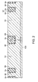
- Fig. 2 there is shown a state where, in the SiO 2 film being the insulating coating film 110 after the modification, the SiO 2 film on the n-well 51 and the p-well 52 of the silicon substrate 100 has been etched.
- an STI element isolation region 2a made of SiO 2 obtained by completely modifying SiCO remains in the shallow trench 57.
- a surface of the STI isolation region 2a in the shallow trench 57 is flush with the surface of the silicon substrate 100. This is because the SiO 2 film can be etched using the silicon substrate 100 as an etching stopper.
- the SiCO film according to this invention does not require CMP, not only can it be used as the surface-flattened film having the flat surface, it can also form the STI element isolation region excellent in insulating properties with no voids.
- the permittivity of the element isolation region 2a is 4.0 equal to that of SiO 2 .
- the SiCO film according to this invention can obtain not only the effect of forming the STI isolation region 2a, but also an effect of making CMP unnecessary and achieving a low permittivity when applied to formation of an interlayer insulating film.
- a description will be given, as an embodiment 2, the case where the SiCO film according to this invention is used as a lowermost-layer interlayer insulating film.
- Fig. 3 In the structure of Fig. 2 in which the STI element isolation region 2a formed by heat-treating the insulating coating film 110 is buried in the shallow trench 57, respective regions forming semiconductor elements are formed as shown in Fig. 3 .
- gate insulating films 70 made of silicon nitride (Si 3 N 4 ) are formed on the surfaces of the n-well 51 and the p-well 52 (which are element forming regions, respectively) surrounded by the STI element isolation region 2a and a gate electrode 72 is mounted on each gate insulating film 70. Side surfaces and a surface of each gate electrode 72 and gate insulating film 70 are covered with an oxide film 17.
- p-type element regions (source and drain regions) 74 formed by implanting p-type impurities are provided at the surface of the n-well 51, while n-type element regions (source and drain regions) 76 formed by implanting n-type impurities are provided at the surface of the p-well 52.
- a silicide layer 77 for contact is formed at the surface of each of the element regions (source and drain regions) 74 and 76.
- the distance between the gate electrodes 72 of two MOS transistors formed on each of the n-well 51 and the p-well 52 is 45nm.
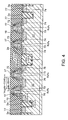
- an insulating coating film 18 made of SiCO is coated as an interlayer insulating film on the surfaces of the element forming regions of the silicon substrate 100 and the STI element isolation region 2a so as to bury therein the gate electrodes 72 and the oxide films 17 covering the side surfaces and the surfaces of the gate electrodes 72.
- the insulating coating film 18 is the same as the SiCO film used for forming the STI isolation region 2a.
- the coated insulating coating film 18 absorbs unevenness formed due to the protrusion of the gate electrodes to exhibit the surface flatness, has a high insulation resistance, and has an extremely low relative permittivity k of about 2.4 by adjusting the temperature in baking.
- the lowermost-layer interlayer insulating film covering the gate electrodes 72 protruding from the silicon substrate 100 is formed by coating the insulating coating film 18. Since, as described with respect to the STI element isolation region 2a, the insulating coating film 18 formed of SiCO is a coating film having fluidity, even if it is coated on the surface, with the unevenness such as the gate electrodes 72, of the silicon substrate 100, it does not reflect the surface unevenness of the silicon substrate 100 and thus its surface maintains the flatness.
- the insulating coating film 18 shown in Fig. 4 has the lower relative permittivity k as compared with the SiO 2 film.
- the insulating coating film 18 formed of SiCO maintains high flatness, it is not necessary to carry out flattening by CMP. Further, since it is possible to reduce the relative permittivity k of the interlayer insulating film, the high-speed operation of the device is not impaired. By reducing the relative permittivity, it is possible to reduce the parasitic capacitance of the electrodes and wiring and thus to achieve high-speed transmission of signals.
- the interlayer insulating film 18 shown in Fig. 4 may be configured such that the interlayer insulating film 18 is provided with through holes reaching the contact layers 77 of the source/drain regions 74 and 76 and the gate electrodes 72, electrode lead-out conductors electrically connected to the contact layers 77 and the gate electrodes 72, respectively, are provided in the through holes, and wiring layers electrically connected to these conductors are provided on a surface of the interlayer insulating film 18, thereby forming a semiconductor device.
- a smooth film 21 made of SiCO is further coated as a second-layer interlayer insulating film by spin coating on the interlayer insulating film 18 formed by the above-mentioned technique.
- the illustrated smooth film 21 is obtained by baking and annealing SiCO at a low temperature of about 400oC and, as a result, has a relative permittivity k of 2.4. Therefore, also in this example, the relative permittivity k of the interlayer insulating film can be reduced.
- electrode lead-out conductors 78 to the contact layers 77 and gate wirings 19 to the gate electrodes 72 of the MOS transistors are formed by applying normal techniques such as resist coating, exposure, and etching to the lowermost-layer interlayer insulating film 18 and, further, wirings 8 respectively connected to the source/drain regions of the MOS transistors are buried in via holes of the smooth film 21.
- a conductive barrier layer 7 of TiN, TaN, or the like is preferably formed in each via hole as an underlayer for Cu or W.
- a multilayer interlayer insulating film is further formed.
- a first barrier layer 24 made of SiCO is formed by CVD on the smooth film 21 being a second-layer interlayer insulating film formed of SiCO and then a fluorocarbon (CFx) film 25 is formed as a third-layer interlayer insulating film.
- a second SiCO barrier layer 26 is formed by CVD on the CFx film 25 as the third-layer interlayer insulating film and a low relative permittivity CFx film 27 is formed as a fourth interlayer insulating film on the second barrier layer 26.
- a third SiCO barrier layer 28 is formed by CVD on the CFx film 27.
- wirings 31 are formed through the CFx films 25 and 27 forming the third and fourth interlayer insulating films and the first to third CVD insulator barrier layers 24, 26, and 28 and a conductive barrier layer 30 is provided as an underlayer for each wiring 31.
- a second-layer interlayer insulating film 21, a third-layer interlayer insulating film 32, and a fourth-layer interlayer insulating film 33 are each formed by a SiCO film obtained by coating the above-mentioned SiCO and heat-treating it at a low temperature of 400oC.
- the second-layer to fourth-layer interlayer insulating films 21, 32, and 33 each have a relative permittivity of 2.4 equal to that of the lowermost-layer interlayer insulating film 18.
- wirings 31 respectively connected to the source/drain regions of the MOS transistors, and barrier layers 30 serving as underlayers for the wirings 31.
- an insulating barrier layer 34 in the form of a SiCN film is provided on the lowermost-layer interlayer insulating film 18 having a relative permittivity k of 2.4 and a second-layer interlayer insulating film 21 formed by coating SiCO is coated on the insulating barrier layer 34.
- the SiCN film 34 is formed by CVD and has a relative permittivity k of 4.0, for example.
- FIG. 9 there is shown a state where electrodes and wirings are formed in the multilayer-structure interlayer insulating film shown in Fig. 8 .
- gate electrode wirings are respectively formed for the gate electrodes 72 of the MOS transistors and, further, via holes penetrating the lowermost-layer interlayer insulating film 18, the SiCN film 34, and the second-layer interlayer insulating film 21 are respectively formed for the source/drain regions of the MOS transistors and, in each via hole, a conductive barrier layer 22 and a wiring 23 are formed.
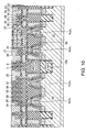
- third-layer and fourth-layer interlayer insulating films 25 and 27 are respectively formed on barrier layers 35 and 36 formed of SiCN. Further, a SiCN barrier layer 37 is formed also on the fourth-layer interlayer insulating film 27.
- the insulating barrier layers 34, 35, 36, and 37 are formed of SiCN having a relative permittivity k of 4.0, while the interlayer insulating films 18 and 21 are each formed by the SiCO film having a relative permittivity of 2.4 and the interlayer insulating films 25 and 27 are each formed by the CFx film having a relative permittivity k of 1.9.
- the lowermost-layer interlayer insulating film 18 is formed by the SiCO coating film that does not require flattening by CMP. Accordingly, it is not necessary to flatten the surface of the lowermost-layer interlayer insulating film 18 by CMP or the like.
- the manufacturing method according to this invention since it is possible to minimize the number of times of using CMP, the cost required for CMP can be reduced. Further, since it is possible to reduce the relative permittivity k of the entire multilayer-structure interlayer insulating film, the stray capacitance and the leakage current can be prevented.
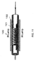
- the baking evaluation test was performed using an infrared baking furnace 120. Specifically, baking was carried out by passing a tray with silicon wafer samples 122 placed thereon in the infrared baking furnace 120 provided with IR lamps 121. The baking temperature range was 300°C to 800oC. The baking was carried out in four kinds of gas atmospheres, i.e. N 2 ; N 2 80%+O 2 20%; O 2 100%; and O 2 100%+H 2 O3%. In this case, the gas flow rates were 1 slm (linear velocity: 0.6cm/sec) and 5slm (linear velocity: 3.0cm/sec).
- Fig. 12 there is shown the relationship between the surface roughness (Ra and peak-to-valley (P-V) value) of the insulating coating film according to this invention and the heating profile.
- Fig. 12 shows the relationship between the surface roughness and the heating rate at 400oC, 600oC, and 800oC.
- the surface roughness when heated to 400oC at 20oC/min is given by Ra (Rah1) and a P-V value (PVh1)
- Ral1 and PV11 the surface roughness when heated to 400oC at 2 to 5oC/min.
- the surface roughness when heated to 600oC at 20oC/min is given by Rah2 and PVh2, while the surface roughness when heated to 600oC at 2 to 5oC/min is given by Ral2 and PVI2.
- the surface roughness when heated to 800oC at 20oC/min is given by Rah3 and PVh3, while the surface roughness when heated to 800oC at 2 to 5oC/min is given by Ral3 and PVI3.
- Fig. 12 shows the relationship between the baking temperature and the thickness (right scale) of the insulating coating film, wherein it is seen that the thickness of the insulating coating film tends to decrease as the baking temperature increases.
- FIG. 13 the relationship between the baking temperature and the surface roughness (Ra, P-V) is shown along with actual AFM (Atomic Force Microscope) images and SEM (Scanning Electron Microscope) images.
- Ra and the P-V value when heated to 400oC at a heating rate of 20oC/min are 0.2783nm and 2.837nm, respectively, thus having a surface as shown in the AFM image.
- SEM image an aluminum film formed on the insulating coating film designated by U has a rough surface.
- the baking temperature is set to 300 to 900oC (preferably 400oC to 800oC).
- the flatness of a surface-flattened film is improved by high-temperature baking (800oC), but the film thickness tends to decrease.
- Fig. 14 the relationship between the thickness of the insulating coating film and the spin-coating rotation speed is shown along with the relationship between the relative permittivity k of the insulating coating film and the spin-coating rotation speed. As shown in Fig. 14 , it is seen that the thickness of the insulating coating film decreases from 270nm to 100nm as the spin-coating rotation speed increases from 600rpm to 4000rpm, while the relative permittivity k is substantially constant (2.4) regardless of the spin-coating rotation speed.
- Fig. 15 there are shown the current-voltage characteristics of a surface-flattened film obtained by baking at 400oC the insulating coating film coated to a thickness of 170nm at a rotation speed of 1300rpm.
- the surface-flattened film according to this invention exhibits a current characteristic of 1.0 ⁇ 10 -8 (A/cm 2 ) or less at a voltage of 4.0 (MV/cm) or less and, as a result of this, it is seen that it has high insulating properties.
- the relative permittivity k of the surface-flattened film shown in Fig. 15 is 2.282.
- a surface-flattened film obtained by baking at 400oC the insulating coating film coated to a thickness of 270nm at a rotation speed of 600rpm exhibits similar current-voltage characteristics.
- the dielectric film with no change in permittivity or smoothness even if the thickness is changed and with a voltage resistance of 10 (MV/cm) even if the thickness is reduced (100nm) and it has been found that when the thickness is reduced, current variations occur if the electrode area increases.
- the suffix of first "O" in the general formula is 2-(n/2).
- a semiconductor device manufacturing method of this invention can reduce the number of times of CMP and thus is applicable to various semiconductor devices including STI and/or an interlayer insulating film of a multilayer structure.
Landscapes
- Internal Circuitry In Semiconductor Integrated Circuit Devices (AREA)
- Element Separation (AREA)
- Formation Of Insulating Films (AREA)
- Insulated Gate Type Field-Effect Transistor (AREA)
- Wire Bonding (AREA)
Abstract
In manufacturing processes of a semiconductor device including a shallow trench element isolation region and an interlayer insulating film of a multilayer structure, it is necessary to repeatedly use CMP, but since the CMP itself is costly, the repeated use of the CMP is a cause to increase the manufacturing cost.
As an insulating film for use in a shallow trench (ST) element isolation region and/or a lowermost-layer interlayer insulating film, use is made of an insulating coating film that can be coated by spin coating. The insulating coating film has a composition expressed by ((CH3)nSiO2-n/2)x(SiO2)1-x (where n=1 to 3 and 0≤x≤1.0) and a film with a different relative permittivity k is formed by selecting heat treatment conditions. The STI element isolation region can be formed by modifying the insulating coating film completely to a SiO2 film, while the interlayer insulating film with a small relative permittivity k can be formed by converting it to a state not completely modified.
Description
- This invention relates to a semiconductor device and its manufacturing method and, in particular, relates to a semiconductor device having one or both of a shallow trench isolation (hereinafter abbreviated as STI) structure and an interlayer insulating film structure and to its manufacturing method.
- A semiconductor device having an STI structure is configured such that an element isolation region made of an insulating film is formed in a shallow trench (shallow trench) provided on a surface of a semiconductor substrate and semiconductor elements are formed in a plurality of element forming regions isolated from each other by the element isolation region. On the other hand, a semiconductor device having an interlayer insulating film structure is configured such that at least one interlayer insulating film is provided over a surface of a semiconductor substrate and an element isolation region, an electrode layer is formed to penetrate the interlayer insulating film so as to be electrically connected to at least one of a plurality of regions forming each of semiconductor elements, and a wiring layer is formed on the interlayer insulating film so as to be electrically connected to the electrode layer. In general, a normal semiconductor LSI has both of these two structures.
- Both structures are common in that a CMP (chemical-mechanical polishing) process is required. That is, in order to form each of the structures, it is essential to perform the CMP process in the manufacture of conventional semiconductor devices. In the formation of the STI structure, the insulating film is formed on the semiconductor substrate including the shallow trench and, since unevenness of the trench appears on a surface of the insulating film, a technique is employed that flattens the surface of the insulating film by CMP to cause the insulating film to remain only in the shallow trench, thereby forming the element isolation region. On the other hand, the interlayer insulating film is often formed by CVD using BPSG (boro-phospho-silicate glass) as a material thereof. In this case, since unevenness of the surface of the semiconductor substrate before the CVD formation (e.g. due to the protrusion of gate electrode portions) appears on a surface of the BPSG film, it is necessary, after forming the BPSG film, to polish its surface by CMP to flatten it. After flattening it, the formation of the penetrating electrode layer and the formation of the wiring layer on the interlayer insulating film are carried out as described above. Further, when a second-layer interlayer insulating film is provided over such an interlayer insulating film, its surface is also flattened by CMP.
- In the case of the semiconductor device having the STI structure and the interlayer insulating film structure, it is necessary to repeat CMP a number of times. Since the CMP process itself is a costly process as compared with etching or the like, the repetition of CMP is a cause to increase the cost of semiconductor devices to be manufactured.
- Further, when BPSG forming the interlayer insulating film is polished by CMP, since there is no stopper for the BPSG, there is a possibility that the BPSG is excessively polished to damage gate electrodes. Therefore, it is necessary to carry out the CMP in a state with an extra margin and thus there is a drawback that the thickness of the BPSG should be large.
-
Patent Document 1 discloses, as a process of burying an STI trench with an insulating film, a process that coats a solution of polysilazane or the like on a silicon substrate to bury an STI trench with the solution and then converts the solution to a SiO2 film for element isolation by a high-temperature treatment (Patent Document 1, paragraph 0009). - Patent Document 2 discloses, as a substitute process for a BPSG process, a process that cures a spin-on-glass film containing polysilazane by the use of an oxidant solution and then converts it to a silicon oxide film by a heat treatment, thereby forming the silicon oxide film. In order to improve the flatness of a surface of the formed silicon oxide film, Patent Document 2 also discloses that further processing such as a CMP process, a dry etching process, or a wet etching process is applied to the silicon oxide film.
-
- Patent Document 1:
-
JP-A-2005-285818 - Patent Document 2:
-
JP-A-2005-45230 - According to
Patent Document 1, by the use of the coating film using polysilazane as its material, even if the aspect ratio of the shallow trench is high, the shallow trench can be uniformly buried (Patent Document 1, paragraph 0048). However,Patent Document 1 points out that a CMP process for surface polishing is essential for leaving the element isolation region in the shallow trench. In other words,Patent Document 1 does not point out the problem followed by the CMP process. - Patent Document 2 discloses forming the insulating coating film in the form of the spin-on-glass film containing polysilazane by the coating formation. However, the spin-on-glass film shown in Patent Document 2 has a large number of voids and thus cannot be used as it is, and hence, further processing is essential for improving the flatness. Therefore, various processes are required to increase the cost.
- Further,
Patent Documents 1 and 2 each only disclose converting the insulating coating film completely to the silicon oxide film, but fail to pay attention to reducing the permittivity of the interlayer insulating film. Further, neither of them suggests anything about producing films with mutually different properties from a single insulating coating film. - Therefore, it is a technical object of this invention to provide a semiconductor device that makes it possible to form an element isolation region and/or an interlayer insulating film without performing CMP, and a method of manufacturing the semiconductor device.
- It is a further technical object of this invention to provide a semiconductor device that makes it possible to reduce the manufacturing cost, and a method of manufacturing the semiconductor device.
- It is another technical object of this invention to provide a semiconductor device in which an interlayer insulating film having a low permittivity is formed without CMP, and a method of manufacturing the semiconductor device.
- It is still another technical object of this invention to provide a semiconductor device in which an element isolation region and an interlayer insulating film having mutually different permittivities are formed from the same composition, and a method of manufacturing the semiconductor device.
- According to the invention, therei obtained a semiconductor device comprising an element isolation region, wherein :said element isolation region includes an insulating film made of SiO2 obtained by modifying, by a heat treatment, a coating film comprising one kind or two or more kinds of compositions expressed by a general formula of ((CH3)nSiO2-n/2)x(SiO2)1-x (where n=1 to 3 and 0≤x≤1.0).
- Moreove, in accordance with the present invention, there is obtained a semiconductor device, wherein said insulating film has a surface flatness of 0.27µm or less in Ra and 2.6µm or less in P-V (peak-to-valley) value.
- Further, in accordance with the present invention, there is obtained a semiconductor device, wherein said element isolation region has a depth of 0.26µm or less and a width of 0.22µm or less.
- According to the invention, there is obtained a semiconductor device, wherein said insulating film has a flatness of a degree that does not require CMP.
- According to the invention, there is obtained a method of manufacturing a semiconductor device comprising an element isolation region, said method comprising: a step of forming a shallow trench on a semiconductor substrate for forming said element isolation region, a step of coating a coating film on said semiconductor substrate including said shallow trench, anda step of modifying said coating film to an element isolation insulator, wherein said coating film comprises one kind or two or more kinds of compositions expressed by a general formula of ((CH3)nSiO2-n/2)x(SiO2)1-x (where n=1 to 3 and 0≤x≤1.0), and said step of modifying is a step of modifying said coating film to a SiO2 film by a heat treatment.
- According to the invention, there is obtained a method of manufacturing a semiconductor device, wherein said heat treatment is performed at a temperature of 800 to 900ºC.
- According to the invention there is obtained a method of manufacturing a semiconductor device, said method further comprising a step of causing a surface of said modified SiO2 film to be equal in height to a surface of said semiconductor substrate without performing CMP.
- According to the invention, there is provided a method of manufacturing a semiconductor device, wherein said step of causing a surface of said modified SiO2 film to be equal in height to a surface of said semiconductor substrate is an etching step.
- According to the invention, there is obtained a method of manufacturing a semiconductor device, said method further comprising a step of forming an interlayer insulating film, wherein said step of forming an interlayer insulating film comprises a step of coating a coating film comprising one kind or two or more kinds of compositions expressed by a general formula of ((CH3)nSiO2-n/2)x(SiO2)1-x (where n=1 to 3 and 0≤x≤1.0) and a step of heat-treating said coating film at a temperature equal to or less than the temperature in said step of modifying.
- According to the invention, there is obtained a method of manufacturing a semiconductor device, wherein the temperature equal to or less than the temperature in said step of modifying is a temperature of 600ºC or less.
- According to the invention, there is obtained a method of manufacturing a semiconductor device, wherein the temperature equal to or less than the temperature in said step of modifying is a temperature of 400ºC or less.
- According to the invention, there is obtained a method of manufacturing a semiconductor device, wherein said step of forming an interlayer insulating film is performed after a step of forming a source region and a drain region in an element forming region of said semiconductor substrate defined by said element isolation region and a step of forming a gate electrode on said element forming region through a gate insulating film and comprises said step of coating a coating film so as to bury said gate electrode.
- According to the invention, there is obtained a method of manufacturing a semiconductor device, said method comprising, after said step of forming an interlayer insulating film, a step of forming an electrode reaching at least one of said source region and said drain region, said electrode penetrating said interlayer insulating film.
- According to the invention, there is obtained a semiconductor device comprising an interlayer insulating film of a multilayer structure, said semiconductor device wherein a lowermost layer of said interlayer insulating film includes a coating film expressed by a general formula of ((CH3)nSiO2-n/2)x(Si2)1-x (where n=1 to 3 and 0≤x≤1.0).
- According to the invention, there is obtained a semiconductor device, wherein an interlayer insulating film as said lowermost layer is an insulating film burying therein a gate electrode of said semiconductor device.
- According to the invention, there is obtained a semiconductor device, wherein an electrode reaching at least one of a source region and a drain region of a semiconductor substrate is provided so as to penetrate said interlayer insulating film as said lowermost layer.
- According to the invention, there is obtained a semiconductor device, wherein said interlayer insulating film has a permittivity lower than that of SiO2.
- According to the invention, there is obtained a semiconductor device, wherein the permittivity of said interlayer insulating film is 2.0 to 2.7.
- According to the invention, there is obtained a semiconductor device, wherein the permittivity of said interlayer insulating film is 2.2 to 2.5.
- According to the invention, there is obtained a semiconductor device, wherein an element isolation region formed in a semiconductor substrate is provided under said interlayer insulating film as said lowermost layer and said element isolation region includes a SiO2 film formed by modifying a coating film comprising one kind or two or more kinds of compositions expressed by a general formula of ((CH3)nSiO2-n/2)x(SiO2)1-x (where n=1 to 3 and 0≤x≤1.0).
- According to the invention, there is obtained a semiconductor device manufacturing method comprising a step of forming a plurality of semiconductor elements on a semiconductor substrate, a step of forming a first interlayer insulating film on said semiconductor substrate, a step of forming an electrode layer that penetrates said first interlayer insulating film so as to be electrically connected to at least one of a plurality of regions forming each of said semiconductor elements, and a step of forming a first wiring layer on said first interlayer insulating film so as to be electrically connected to said electrode layer, wherein said step of forming a first interlayer insulating film comprises a step of coating a first coating film comprising one kind or two or more kinds of compositions expressed by a general formula of ((CH3)nSiO2-n/2)x(SiO2)1-x (where n=1 to 3 and 0≤x≤1.0) and a step of forming a first insulating film having a predetermined permittivity by heat-treating said first coating film at a predetermined temperature.
- According to the invention, there is obtained a semiconductor device manufacturing method, wherein said predetermined temperature is a temperature of 400ºC or less.
- According to the invention, there is obtained a semiconductor device manufacturing method, wherein said predetermined permittivity is a permittivity lower than that of SiO2.
- According to the invention, there is obtained a semiconductor device manufacturing method, wherein said predetermined permittivity is 2.0 to 2.7.
- According to the invention, there is obtained a semiconductor device manufacturing method, wherein said predetermined permittivity is 2.2 to 2.5.
- According to the invention, there is obtained a semiconductor device manufacturing method, wherein said plurality of regions forming each of said semiconductor elements include a source region, a drain region, and a gate electrode.
- According to the invention, there is obtained a semiconductor device manufacturing method, further comprising a step of forming a second interlayer insulating film on said first interlayer insulating film so as to cover said first wiring layer, a step of forming a first conductor VIA layer that penetrates said second interlayer insulating film so as to be electrically connected to at least part of said first wiring layer, and a step of forming a second wiring layer on said second interlayer insulating film so as to be electrically connected to said first conductor VIA layer.
- According to the invention, there is obtained a semiconductor device manufacturing method, wherein said step of forming a second interlayer insulating film comprises a step of coating a second coating film comprising one kind or two or more kinds of compositions expressed by a general formula of ((CH3)nSiO2-n/2)x(SiO2)1-x (where n=1 to 3 and 0≤x≤1.0) and a step of forming a second insulating film having a predetermined permittivity by heat-treating said second coating film at a predetermined temperature.
- According to the invention, there is obtained a semiconductor device manufacturing method, wherein said step of forming a first wiring layer on said first interlayer insulating film is performed without treating a surface of said first interlayer insulating film by CMP.
- According to the invention, there is obtained a semiconductor device manufacturing method according to
claim 28, wherein said step of forming a second wiring layer on said second interlayer insulating film is performed without treating a surface of said second interlayer insulating film by CMP. - According to the invention, there is obtained a semiconductor device manufacturing method, wherein a step of forming a shallow trench on said semiconductor substrate, a step of forming an element isolation region in said shallow trench, and a step of forming said plurality of regions forming each of said semiconductor elements are performed before said step of forming a first interlayer insulating film on said semiconductor substrate.
- According to the invention, there is obtained a semiconductor device manufacturing method, wherein said step of forming said plurality of regions forming each of said semiconductor elements comprises a step of forming a source region and a drain region in an element forming region of said semiconductor substrate defined by said element isolation region and a step of forming a gate electrode on said element forming region through a gate insulating film.
- According to the invention, there is obtained a semiconductor device manufacturing method, wherein said step of forming an element isolation region comprises a step of coating a third coating film comprising one kind or two or more kinds of compositions expressed by a general formula of ((CH3)nSiO2-n/2)x(SiO2)1-x (where n=1 to 3 and 0≤x≤1.0) so as to bury at least said shallow trench and a step of modifying said third coating film to SiO2.
- According to the invention, there is obtained a semiconductor device manufacturing method, wherein said step of modifying to SiO2 comprises a step of baking and annealing said coated third coating film at 800ºC to 900ºC.
- According to the invention, there is obtained a method of manufacturing a semiconductor device comprising an element isolation region and an interlayer insulating film, wherein mutually different heat treatments are applied to the same composition, thereby forming said element isolation region and said interlayer insulating film having mutually different permittivities.
- According to the invention, there is obtained a method of manufacturing a semiconductor device, wherein said composition comprises one kind or two or more kinds of compositions expressed by a general formula of ((CH3)nSiO2-n/2)x(SiO2)1-x (where n=1 to 3 and 0≤x≤1.0).
- According to the invention, there is obtained a method of manufacturing a semiconductor device, wherein formation of said element isolation region and said interlayer insulating film includes no CMP process.
- According to the invention, there is obtained a semiconductor device comprising a semiconductor substrate, a semiconductor element having a plurality of regions and formed on said semiconductor substrate, a first interlayer insulating film formed on said semiconductor substrate, an electrode layer penetrating said first interlayer insulating film so as to be electrically connected to at least one of said plurality of regions, and a first wiring layer provided on said first interlayer insulating film so as to be electrically connected to said electrode layer, wherein said first interlayer insulating film includes a first coating film comprising one kind or two or more kinds of compositions expressed by a general formula of ((CH3)nSiO2-n/2)x(SiO2)1-x (where n=1 to 3 and 0≤x≤1.0).
- Preferably, said semiconductor element includes a gate electrode formed on said semiconductor substrate through a gate insulating film and said first interlayer insulating film buries said gate electrode therein.
- In a preferred aspect, said plurality of regions include a source region and a drain region and said electrode layer is electrically connected to at least one of said source region and said drain region.
- Preferably, said inerlater insulating film has a permittivity lower than that of SiO2.
- According to a manufacturing method of this invention, it is possible to form an element isolation region and/or an interlayer insulating film without using CMP and thus to reduce the manufacturing cost of a semiconductor device.
- According to this invention, it is possible to form insulating films having different permittivities from a single composition by changing the heat treatment temperature and thus to simplify the manufacturing processes.
-
-
Fig. 1 is a sectional view explaining a process of spin-coating an insulating coating film in manufacturing processes of a semiconductor device according to this invention. -
Fig. 2 is a diagram for explaining anembodiment 1 of this invention, wherein there is shown a sectional view explaining an STI element isolation region using the insulating coating film shown inFig. 1 . -
Fig. 3 is a sectional view explaining manufacturing processes of the semiconductor device including the STI element isolation structure formed according to this invention. -
Fig. 4 is a diagram for explaining an embodiment 2 of this invention, wherein there is shown a sectional view explaining a coating process of a lowermost-layer interlayer insulating film carried out after the processes ofFig. 3 . -
Fig. 5 is a sectional view exemplarily explaining processes carried out after the processes of the embodiment 2 of this invention. -
Fig. 6 is a sectional view showing another example of processes carried out after the processes of the embodiment 2 of this invention. -
Fig. 7 is a sectional view showing still another example of processes carried out after the processes of the embodiment 2 of this invention. -
Fig. 8 is a sectional view showing an example of processes carried out after the processes of the embodiment 2 of this invention, wherein there is shown an example of an interlayer insulating film of a multilayer structure. -
Fig. 9 is a sectional view showing another example of processes carried out after the processes of the embodiment 2 of this invention, wherein there is shown another example of an interlayer insulating film of a multilayer structure. -
Fig. 10 is a sectional view showing another example of processes carried out after the processes of the embodiment 2 of this invention, wherein there is shown still another example of an interlayer insulating film of a multilayer structure. -
Fig. 11 is a schematic diagram showing equipment used in a baking evaluation of an insulating coating film according to this invention. -
Fig. 12 is a diagram showing the relationship between the baking temperature and the surface roughness and thickness of the film when baking is carried out using the equipment shown inFig. 11 . -
Fig. 13 is a diagram showing the relationship between the rising rate of the baking temperature and the surface roughness of the insulating coating film according to this invention along with images. -
Fig. 14 is a diagram showing the relationship between the spin-coating rotation speed and the thickness and relative permittivity k of the insulating coating film according to this invention. -
Fig. 15 is a diagram explaining the electrical properties of the insulating coating film according to this invention. - Hereinbelow, embodiments of this invention will be described with reference to the drawings.
-
Fig. 1 is a sectional view showing part of manufacturing processes of a semiconductor device using surface-flattened coating films (smoothed films) according to this invention. Specifically, in asilicon substrate 100, there are provided an n-well 51 formed by implanting phosphorus (P) and a p-well 52 formed by implanting boron (B). - Further, a shallow trench (ST) 57 for element isolation is formed on a surface of a boundary portion between the n-well 51 and the p-well 52 and surfaces of the n-well and the p-well. The illustrated
shallow trench 57 has a width of 0.22µm and a depth of 0.25µm. - The surfaces of the n-well 51 and the p-well 52 are formed with a SiO2 film 11 and a bottom surface and side surfaces of the
shallow trench 57 are also formed with a SiO2 film 58. - An insulating
coating film 110 according to this invention is coated on the illustrated SiO2 films 11 and 58. The insulatingcoating film 110 is formed by coating a material having a composition of (CH3SiO3/2)x(SiO2)1-x (where 0≤x≤1.0). - As is clear from the composition (CH3SiO3/2)x(SiO2)1-x of the insulating
coating film 110, the insulating coating film contains Si, C, and O and the ratio of the numbers of these component atoms is O>Si≥C. The insulatingcoating film 110 contains a methyl group (CH3) and the methyl group is liberated in air at 480ºC but is not liberated in N2 even at 600ºC. Herein, if x=1.0, i.e. in a state of only a CH3SiO3/2 component, the relative permittivity k of the insulating coating film is 2.0, if x=0.9, k is 2.1, if x=0.7, k is 2.3, and if x=0.5, k is 2.7. As a coating solution, use is made of one in which 5wt% or more of the above-mentioned composition is dissolved in a solvent and, after coating it, heating is applied under a reduced pressure to completely remove the solvent. If heating is applied at 500ºC under a reduced pressure of 1 to 4Torr, the insulating coating film with k of 2.0 to 2.1 is obtained and, if heating is applied at 400ºC under a reduced pressure of 1 to 5Torr, the insulating coating film with k of 2.3 to 2.7 is obtained. If heating is applied at 800ºC, the methyl group is liberated so that the insulatingcoating film 110 is modified to SiO2 and, only with the SiO2, the relative permittivity k becomes 4.0. The insulating properties of this SiO2 exhibit excellent values of 1×10⁻¹⁰ (A/cm2) at 1 (MV/cm), 1×10⁻⁹ (A/cm2) at 3 (MV/cm), and 1×10⁻⁸ (A/cm2) even at 5 (MV/cm). - Hereinbelow, the above-mentioned insulating coating film and its composition may be abbreviated as a SiCO film and SiCO, respectively. Since the coating solution forming the insulating coating film (SiCO film) 110 is in a liquid state at ordinary temperature, the insulating
coating film 110 can be spin-coated on the semiconductor substrate and has fluidity in a coated state so that it does not reflect unevenness of the bottom surface and thus has high flatness. - Herein, when the insulating
coating film 110 is baked and annealed at 900ºC, it is modified to SiO2 (k=4.0) free of gas generation and thermal contraction and excellent in heat resistance. Therefore, if it is necessary to modify the insulatingcoating film 110 completely to a SiO2 film, such complete modification is enabled. Thus, by selecting heat treatment conditions of the insulatingcoating film 110 formed by the SiCO film, it is possible to form a surface-flattened film having a permittivity in the range of k=2.0 to 4.0. - Referring back to
Fig. 1 , the insulatingcoating film 110 is formed by spin-coating SiCO on thesilicon substrate 100 and has a relative permittivity of 2.4 in this state. Since the insulatingcoating film 110 made of SiCO has fluidity upon coating, its surface can be maintained flat without being affected by unevenness on thesilicon substrate 100 due to theshallow trench 57, the SiO2 film 58, and so on. - Then, when etching the surface-flattened film obtained by baking the insulating
coating film 110 formed of SiCO, since the surface-flattened film can be clearly distinguished from a silicon nitride film (Si3N4), thesilicon substrate 100, or the like, it can be etched by providing the silicon nitride film (Si3N4) on the SiO2 film 11 and using it as a stopper or by using thesilicon substrate 100 as a stopper. Therefore, the surface-flattened film formed of SiCO can be uniformly removed, while maintaining the flatness of its surface, only by etching without using CMP. - The insulating
coating film 110 shown inFig. 1 is, after the coating, baked and annealed at a temperature of 800ºC to 900ºC. As a result of this heat treatment, the insulatingcoating film 110 is modified to SiO2. After the modification, the insulatingcoating film 110 becomes a SiO2 film with a flat surface maintained. - Referring to
Fig. 2 , there is shown a state where, in the SiO2 film being the insulatingcoating film 110 after the modification, the SiO2 film on the n-well 51 and the p-well 52 of thesilicon substrate 100 has been etched. - In this case, an STI
element isolation region 2a made of SiO2 obtained by completely modifying SiCO remains in theshallow trench 57. - As shown in
Fig. 2 , a surface of theSTI isolation region 2a in theshallow trench 57 is flush with the surface of thesilicon substrate 100. This is because the SiO2 film can be etched using thesilicon substrate 100 as an etching stopper. - Since the SiCO film according to this invention does not require CMP, not only can it be used as the surface-flattened film having the flat surface, it can also form the STI element isolation region excellent in insulating properties with no voids. The permittivity of the
element isolation region 2a is 4.0 equal to that of SiO2. - As is also clear from
Fig. 2 , using SiCO according to this invention, it is possible to form the STIelement isolation region 2a in theshallow trench 57 without performing CMP. - The SiCO film according to this invention can obtain not only the effect of forming the
STI isolation region 2a, but also an effect of making CMP unnecessary and achieving a low permittivity when applied to formation of an interlayer insulating film. Hereinbelow, a description will be given, as an embodiment 2, the case where the SiCO film according to this invention is used as a lowermost-layer interlayer insulating film. - Referring to
Fig. 3 , a description will be given of manufacturing processes of the semiconductor device carried out after forming the STIelement isolation region 2a shown inFig. 2 . - In the structure of
Fig. 2 in which the STIelement isolation region 2a formed by heat-treating the insulatingcoating film 110 is buried in theshallow trench 57, respective regions forming semiconductor elements are formed as shown inFig. 3 . Specifically, as shown inFig. 3 ,gate insulating films 70 made of silicon nitride (Si3N4) are formed on the surfaces of the n-well 51 and the p-well 52 (which are element forming regions, respectively) surrounded by the STIelement isolation region 2a and agate electrode 72 is mounted on eachgate insulating film 70. Side surfaces and a surface of eachgate electrode 72 andgate insulating film 70 are covered with anoxide film 17. - Further, p-type element regions (source and drain regions) 74 formed by implanting p-type impurities are provided at the surface of the n-well 51, while n-type element regions (source and drain regions) 76 formed by implanting n-type impurities are provided at the surface of the p-
well 52. Asilicide layer 77 for contact is formed at the surface of each of the element regions (source and drain regions) 74 and 76. - In the illustrated example, the distance between the
gate electrodes 72 of two MOS transistors formed on each of the n-well 51 and the p-well 52 is 45nm. - Referring to
Fig. 4 , an insulatingcoating film 18 made of SiCO is coated as an interlayer insulating film on the surfaces of the element forming regions of thesilicon substrate 100 and the STIelement isolation region 2a so as to bury therein thegate electrodes 72 and theoxide films 17 covering the side surfaces and the surfaces of thegate electrodes 72. Herein, it is assumed that the insulatingcoating film 18 is the same as the SiCO film used for forming theSTI isolation region 2a. Therefore, like the above-mentioned SiCO used for forming the STIelement isolation region 2a, the coated insulatingcoating film 18 absorbs unevenness formed due to the protrusion of the gate electrodes to exhibit the surface flatness, has a high insulation resistance, and has an extremely low relative permittivity k of about 2.4 by adjusting the temperature in baking. - Specifically, as shown in
Fig. 4 , in the embodiment 2 according to this invention, the lowermost-layer interlayer insulating film covering thegate electrodes 72 protruding from thesilicon substrate 100 is formed by coating the insulatingcoating film 18. Since, as described with respect to the STIelement isolation region 2a, the insulatingcoating film 18 formed of SiCO is a coating film having fluidity, even if it is coated on the surface, with the unevenness such as thegate electrodes 72, of thesilicon substrate 100, it does not reflect the surface unevenness of thesilicon substrate 100 and thus its surface maintains the flatness. Further, when heat-treated at a low temperature of about 400ºC, SiCO of the above-mentioned composition is not modified to a SiO2 film and thus is in a state containing a large amount of a CH3SiO3/2 component. Therefore, the insulatingcoating film 18 shown inFig. 4 has the lower relative permittivity k as compared with the SiO2 film. - As described above, since the insulating
coating film 18 formed of SiCO maintains high flatness, it is not necessary to carry out flattening by CMP. Further, since it is possible to reduce the relative permittivity k of the interlayer insulating film, the high-speed operation of the device is not impaired. By reducing the relative permittivity, it is possible to reduce the parasitic capacitance of the electrodes and wiring and thus to achieve high-speed transmission of signals. - There are a variety of processes after forming the
interlayer insulating film 18 shown inFig. 4 and a semiconductor device manufacturing method according to this invention is applicable to any of them. For example, it may be configured such that theinterlayer insulating film 18 is provided with through holes reaching the contact layers 77 of the source/drain regions gate electrodes 72, electrode lead-out conductors electrically connected to the contact layers 77 and thegate electrodes 72, respectively, are provided in the through holes, and wiring layers electrically connected to these conductors are provided on a surface of theinterlayer insulating film 18, thereby forming a semiconductor device. - Hereinbelow, processes in the case where a multilayer wiring structure is provided over the
interlayer insulating film 18 will be exemplarily described. - Referring to
Fig. 5 , asmooth film 21 made of SiCO is further coated as a second-layer interlayer insulating film by spin coating on theinterlayer insulating film 18 formed by the above-mentioned technique. The illustratedsmooth film 21 is obtained by baking and annealing SiCO at a low temperature of about 400ºC and, as a result, has a relative permittivity k of 2.4. Therefore, also in this example, the relative permittivity k of the interlayer insulating film can be reduced. - In the illustrated example, electrode lead-out
conductors 78 to the contact layers 77 and gate wirings 19 to thegate electrodes 72 of the MOS transistors are formed by applying normal techniques such as resist coating, exposure, and etching to the lowermost-layerinterlayer insulating film 18 and, further,wirings 8 respectively connected to the source/drain regions of the MOS transistors are buried in via holes of thesmooth film 21. As a material of theconductors 78, the gate wirings 19, and thewirings 8, Cu or W can be used. When Cu or W is used, aconductive barrier layer 7 of TiN, TaN, or the like is preferably formed in each via hole as an underlayer for Cu or W. - Referring to
Fig. 6 , there is shown an example in which, after coating asmooth film 21 made of SiCO by spin coating like inFig. 5 after forming the lowermost-layerinterlayer insulating film 18, a multilayer interlayer insulating film is further formed. In the example ofFig. 6 , afirst barrier layer 24 made of SiCO is formed by CVD on thesmooth film 21 being a second-layer interlayer insulating film formed of SiCO and then a fluorocarbon (CFx)film 25 is formed as a third-layer interlayer insulating film. The illustratedCFx film 25 has a relative permittivity k (=1.9) lower than those of theSiCO films - Further, in the illustrated example, a second
SiCO barrier layer 26 is formed by CVD on theCFx film 25 as the third-layer interlayer insulating film and a low relativepermittivity CFx film 27 is formed as a fourth interlayer insulating film on thesecond barrier layer 26. Further, a thirdSiCO barrier layer 28 is formed by CVD on theCFx film 27. As in this example, by forming the interlayer insulating films using the CFx films each having the relative permittivity k still lower than that of the SiCO film baked at the low temperature, the relative permittivity of the entire multilayer-structure interlayer insulating film can be further reduced. - Also in the example shown in
Fig. 6 , wirings 31 are formed through theCFx films conductive barrier layer 30 is provided as an underlayer for eachwiring 31. - Referring to
Fig. 7 , there is shown an example in which the lowermost-layerinterlayer insulating film 18, an uppermost interlayer insulating film, and intermediate interlayer insulating films are all formed by SiCO coating films. In the illustrated example, a second-layerinterlayer insulating film 21, a third-layerinterlayer insulating film 32, and a fourth-layerinterlayer insulating film 33 are each formed by a SiCO film obtained by coating the above-mentioned SiCO and heat-treating it at a low temperature of 400ºC. In this connection, the second-layer to fourth-layerinterlayer insulating films interlayer insulating film 18. - Also in the example shown in
Fig. 7 , like inFig. 6 , there are providedwirings 31 respectively connected to the source/drain regions of the MOS transistors, and barrier layers 30 serving as underlayers for thewirings 31. - In an example shown in
Fig. 8 , an insulatingbarrier layer 34 in the form of a SiCN film is provided on the lowermost-layerinterlayer insulating film 18 having a relative permittivity k of 2.4 and a second-layerinterlayer insulating film 21 formed by coating SiCO is coated on the insulatingbarrier layer 34. In this case, theSiCN film 34 is formed by CVD and has a relative permittivity k of 4.0, for example. - Referring to
Fig. 9 , there is shown a state where electrodes and wirings are formed in the multilayer-structure interlayer insulating film shown inFig. 8 . Specifically, gate electrode wirings are respectively formed for thegate electrodes 72 of the MOS transistors and, further, via holes penetrating the lowermost-layerinterlayer insulating film 18, theSiCN film 34, and the second-layerinterlayer insulating film 21 are respectively formed for the source/drain regions of the MOS transistors and, in each via hole, aconductive barrier layer 22 and awiring 23 are formed. - Referring to
Fig. 10 , over the second-layerinterlayer insulating film 21 shown inFig. 8 , third-layer and fourth-layerinterlayer insulating films barrier layers SiCN barrier layer 37 is formed also on the fourth-layerinterlayer insulating film 27. In this example, the insulating barrier layers 34, 35, 36, and 37 are formed of SiCN having a relative permittivity k of 4.0, while theinterlayer insulating films interlayer insulating films - In each of the examples described above, the lowermost-layer
interlayer insulating film 18 is formed by the SiCO coating film that does not require flattening by CMP. Accordingly, it is not necessary to flatten the surface of the lowermost-layerinterlayer insulating film 18 by CMP or the like. - Therefore, in the manufacturing method according to this invention, since it is possible to minimize the number of times of using CMP, the cost required for CMP can be reduced. Further, since it is possible to reduce the relative permittivity k of the entire multilayer-structure interlayer insulating film, the stray capacitance and the leakage current can be prevented.
- Next, a description will be given of the properties of the SiCO insulating coating film used in this invention.
- First, referring to
Fig. 11 , an apparatus used in a baking evaluation test of an insulating coating film will be described. The baking evaluation test was performed using aninfrared baking furnace 120. Specifically, baking was carried out by passing a tray withsilicon wafer samples 122 placed thereon in theinfrared baking furnace 120 provided withIR lamps 121. The baking temperature range was 300°C to 800ºC. The baking was carried out in four kinds of gas atmospheres, i.e. N2; N280%+O220%;O 2100%; andO 2100%+H2O3%. In this case, the gas flow rates were 1 slm (linear velocity: 0.6cm/sec) and 5slm (linear velocity: 3.0cm/sec). - Referring to
Fig. 12 , there is shown the relationship between the surface roughness (Ra and peak-to-valley (P-V) value) of the insulating coating film according to this invention and the heating profile.Fig. 12 shows the relationship between the surface roughness and the heating rate at 400ºC, 600ºC, and 800ºC. InFig. 12 , the surface roughness when heated to 400ºC at 20ºC/min is given by Ra (Rah1) and a P-V value (PVh1), while the surface roughness when heated to 400ºC at 2 to 5ºC/min is given by Ral1 and PV11. - Further, the surface roughness when heated to 600ºC at 20ºC/min is given by Rah2 and PVh2, while the surface roughness when heated to 600ºC at 2 to 5ºC/min is given by Ral2 and PVI2. Further, the surface roughness when heated to 800ºC at 20ºC/min is given by Rah3 and PVh3, while the surface roughness when heated to 800ºC at 2 to 5ºC/min is given by Ral3 and PVI3.
- As is also clear from
Fig. 12 , it is seen that the surface roughness Ra and P-V value tend to decrease as the heating rate decreases. Therefore, if the insulating coating film is baked at 2 to 5ºC/min, the surface roughness can be made small.Fig. 12 also shows the relationship between the baking temperature and the thickness (right scale) of the insulating coating film, wherein it is seen that the thickness of the insulating coating film tends to decrease as the baking temperature increases. - Referring to
Fig. 13 , the relationship between the baking temperature and the surface roughness (Ra, P-V) is shown along with actual AFM (Atomic Force Microscope) images and SEM (Scanning Electron Microscope) images. As is also clear from the surface roughness (Ra, P-V) and the AFM image, Ra and the P-V value when heated to 400ºC at a heating rate of 20ºC/min are 0.2783nm and 2.837nm, respectively, thus having a surface as shown in the AFM image. Further, as shown in the SEM image, an aluminum film formed on the insulating coating film designated by U has a rough surface. - On the other hand, when the insulating coating film is baked by heating to 400ºC at a heating rate of 5ºC/min, Ra and the P-V value of its surface become 0.2145nm and 2.593nm, respectively, and, as is also clear from the AFM and SEM images, the surface roughness can be made smaller than that when heated at 20ºC/min. Likewise, when the insulating coating film is baked by heating to 600ºC at a heating rate of 2ºC/min, Ra and the P-V value of its surface become 0.2280nm and 2.720nm, respectively, and, when heated to 800ºC at a heating rate of 2ºC/min, Ra and the P-V value become 0.2539nm and 2.602nm, respectively, so that the surface roughness can be improved in both cases as compared with that when heated at 20ºC/min.
- From the evaluation results described above, it has been found that the surface smoothness (surface roughness) is improved to Ra=0.27nm or less by reducing the heating rate in baking to 10ºC/min or less (preferably 1 to 5ºC/min).
- The baking temperature is set to 300 to 900ºC (preferably 400ºC to 800ºC). The flatness of a surface-flattened film is improved by high-temperature baking (800ºC), but the film thickness tends to decrease.
- Referring to
Fig. 14 , the relationship between the thickness of the insulating coating film and the spin-coating rotation speed is shown along with the relationship between the relative permittivity k of the insulating coating film and the spin-coating rotation speed. As shown inFig. 14 , it is seen that the thickness of the insulating coating film decreases from 270nm to 100nm as the spin-coating rotation speed increases from 600rpm to 4000rpm, while the relative permittivity k is substantially constant (2.4) regardless of the spin-coating rotation speed. - Referring to
Fig. 15 , there are shown the current-voltage characteristics of a surface-flattened film obtained by baking at 400ºC the insulating coating film coated to a thickness of 170nm at a rotation speed of 1300rpm. As is also clear fromFig. 15 , the surface-flattened film according to this invention exhibits a current characteristic of 1.0×10⁻⁸ (A/cm2) or less at a voltage of 4.0 (MV/cm) or less and, as a result of this, it is seen that it has high insulating properties. The relative permittivity k of the surface-flattened film shown inFig. 15 is 2.282. Likewise, a surface-flattened film obtained by baking at 400ºC the insulating coating film coated to a thickness of 270nm at a rotation speed of 600rpm exhibits similar current-voltage characteristics. - To sum up the electrical properties of the surface-flattened film, there is obtained the dielectric film with no change in permittivity or smoothness even if the thickness is changed and with a voltage resistance of 10 (MV/cm) even if the thickness is reduced (100nm) and it has been found that when the thickness is reduced, current variations occur if the electrode area increases.
- In the above-mentioned embodiments, the examples are shown in which use is made of the coating film with the composition of (CH3SiO3/2)x(SiO2)1-x (where 0≤x≤1.0). However, in this formula, instead of CH3SiO3/2, use may be made of, for example, (CH3)2SiO, (CH3)3SiO1/2, or the like, or a mixture thereof. That is, this invention is characterized by using a coating film comprising one kind or two or more kinds of compositions expressed by a general formula of ((CH3)nSiO2-n/2)x(SiO2)1-x (where n=1 to 3 and 0≤x≤1.0 Herein, the suffix of first "O" in the general formula is 2-(n/2).
- A semiconductor device manufacturing method of this invention can reduce the number of times of CMP and thus is applicable to various semiconductor devices including STI and/or an interlayer insulating film of a multilayer structure.
Claims (43)
- A semiconductor device comprising an element isolation region, wherein:said element isolation region includes an insulating film made of SiO2 obtained by modifying, by a heat treatment, a coating film comprising one kind or two or more kinds of compositions expressed by a general formula of ((CH3)nSiO2-n/2)x(SiO2)1-x (where n=1 to 3 and 0≤x≤1.0).
- A semiconductor device according to claim 1, wherein said insulating film has a surface flatness of 0.27µm or less in Ra and 2.6µm or less in P-V (peak-to-valley) value.
- A semiconductor device according to claim 1 or 2, wherein said element isolation region has a depth of 0.26µm or less and a width of 0.22µm or less.
- A semiconductor device according to any of claims 1 to 3, wherein said insulating film has a flatness of a degree that does not require CMP.
- A method of manufacturing a semiconductor device comprising an element isolation region, said method comprising:a step of forming a shallow trench on a semiconductor substrate for forming said element isolation region,a step of coating a coating film on said semiconductor substrate including said shallow trench, anda step of modifying said coating film to an element isolation insulator,wherein said coating film comprises one kind or two or more kinds of compositions expressed by a general formula of ((CH3)nSiO2-n/2)x(SiO2)1-x (where n=1 to 3 and 0≤x≤1.0), andsaid step of modifying is a step of modifying said coating film to a SiO2 film by a heat treatment.
- A method of manufacturing a semiconductor device according to claim 5, wherein said heat treatment is performed at a temperature of 800 to 900ºC.
- A method of manufacturing a semiconductor device according to claim 5 or 6, said method further comprising a step of causing a surface of said modified SiO2 film to be equal in height to a surface of said semiconductor substrate without performing CMP.
- A method of manufacturing a semiconductor device according to claim 7, wherein said step of causing a surface of said modified SiO2 film to be equal in height to a surface of said semiconductor substrate is an etching step.
- A method of manufacturing a semiconductor device according to claim 7 or 8, said method further comprising a step of forming an interlayer insulating film, wherein said step of forming an interlayer insulating film comprises a step of coating a coating film comprising one kind or two or more kinds of compositions expressed by a general formula of ((CH3)nSiO2-n/2)x(SiO2)1-x (where n=1 to 3 and 0≤x≤1.0) and a step of heat-treating said coating film at a temperature equal to or less than the temperature in said step of modifying.
- A method of manufacturing a semiconductor device according to claim 9, wherein the temperature equal to or less than the temperature in said step of modifying is a temperature of 600ºC or less.
- A method of manufacturing a semiconductor device according to claim 9, wherein the temperature equal to or less than the temperature in said step of modifying is a temperature of 400ºC or less.
- A method of manufacturing a semiconductor device according to any of claims 9 to 11, wherein said step of forming an interlayer insulating film is performed after a step of forming a source region and a drain region in an element forming region of said semiconductor substrate defined by said element isolation region and a step of forming a gate electrode on said element forming region through a gate insulating film and comprises said step of coating a coating film so as to bury said gate electrode.
- A method of manufacturing a semiconductor device according to claim 12, said method comprising, after said step of forming an interlayer insulating film, a step of forming an electrode reaching at least one of said source region and said drain region, said electrode penetrating said interlayer insulating film.
- A semiconductor device comprising an interlayer insulating film of a multilayer structure, wherein a lowermost layer of said interlayer insulating film includes a coating film expressed by a general formula of ((CH3)nSiO2-n/2)x(SiO2)1-x (where n=1 to 3 and 0≤x≤1.0).
- A semiconductor device according to claim 14, wherein an interlayer insulating film as said lowermost layer is an insulating film burying therein a gate electrode of said semiconductor device.
- A semiconductor device according to claim 14 or 15, wherein an electrode reaching at least one of a source region and a drain region of a semiconductor substrate is provided so as to penetrate said interlayer insulating film as said lowermost layer.
- A semiconductor device according to any of claims 14 to 16, wherein said interlayer insulating film has a permittivity lower than that of SiO2.
- A semiconductor device according to claim 17, wherein the permittivity of said interlayer insulating film is 2.0 to 2.7.
- A semiconductor device according to claim 17, wherein the permittivity of said interlayer insulating film is 2.2 to 2.5.
- A semiconductor device according to any of claims 14 to 19, wherein an element isolation region formed in a semiconductor substrate is provided under said interlayer insulating film as said lowermost layer and said element isolation region includes a SiO2 film formed by modifying a coating film comprising one kind or two or more kinds of compositions expressed by a general formula of ((CH3)nSiO2-n/2)x(SiO2)1-x (where n=1 to 3 and 0≤x≤1.0).
- A semiconductor device manufacturing method comprising a step of forming a plurality of semiconductor elements on a semiconductor substrate, a step of forming a first interlayer insulating film on said semiconductor substrate, a step of forming an electrode layer that penetrates said first interlayer insulating film so as to be electrically connected to at least one of a plurality of regions forming each of said semiconductor elements, and a step of forming a first wiring layer on said first interlayer insulating film so as to be electrically connected to said electrode layer, wherein said step of forming a first interlayer insulating film comprises a step of coating a first coating film comprising one kind or two or more kinds of compositions expressed by a general formula of ((CH3)nSiO2-n/2)x(SiO2)1-x (where n=1 to 3 and 0≤x≤1.0) and a step of forming a first insulating film having a predetermined permittivity by heat-treating said first coating film at a predetermined temperature.
- A semiconductor device manufacturing method according to claim 21, wherein said predetermined temperature is a temperature of 400°C or less.
- A semiconductor device manufacturing method according to claim 21 or 22, wherein said predetermined permittivity is a permittivity lower than that of SiO2.
- A semiconductor device manufacturing method according to claim 21 or 22, wherein said predetermined permittivity is 2.0 to 2.7.
- A semiconductor device manufacturing method according to claim 21 or 22, wherein said predetermined permittivity is 2.2 to 2.5.
- A semiconductor device manufacturing method according to any of claims 21 to 25, wherein said plurality of regions forming each of said semiconductor elements include a source region, a drain region, and a gate electrode.
- A semiconductor device manufacturing method according to any of claims 21 to 26, further comprising a step of forming a second interlayer insulating film on said first interlayer insulating film so as to cover said first wiring layer, a step of forming a first conductor VIA layer that penetrates said second interlayer insulating film so as to be electrically connected to at least part of said first wiring layer, and a step of forming a second wiring layer on said second interlayer insulating film so as to be electrically connected to said first conductor VIA layer.
- A semiconductor device manufacturing method according to claim 27, wherein said step of forming a second interlayer insulating film comprises a step of coating a second coating film comprising one kind or two or more kinds of compositions expressed by a general formula of ((CH3)nSiO2-n/2)x(SiO2)1-x (where n=1 to 3 and 0≤x≤1.0) and a step of forming a second insulating film having a predetermined permittivity by heat-treating said second coating film at a predetermined temperature.
- A semiconductor device manufacturing method according to any of claims 21 to 28, wherein said step of forming a first wiring layer on said first interlayer insulating film is performed without treating a surface of said first interlayer insulating film by CMP.
- A semiconductor device manufacturing method according to claim 28, wherein said step of forming a second wiring layer on said second interlayer insulating film is performed without treating a surface of said second interlayer insulating film by CMP.
- A semiconductor device manufacturing method according to any of claims 21 to 30, wherein a step of forming a shallow trench on said semiconductor substrate, a step of forming an element isolation region in said shallow trench, and a step of forming said plurality of regions forming each of said semiconductor elements are performed before said step of forming a first interlayer insulating film on said semiconductor substrate.
- A semiconductor device manufacturing method according to claim 31, wherein said step of forming said plurality of regions forming each of said semiconductor elements comprises a step of forming a source region and a drain region in an element forming region of said semiconductor substrate defined by said element isolation region and a step of forming a gate electrode on said element forming region through a gate insulating film.
- A semiconductor device manufacturing method according to claim 31 or 32, wherein said step of forming an element isolation region comprises a step of coating a third coating film comprising one kind or two or more kinds of compositions expressed by a general formula of ((CH3)nSiO2-n/2)x(SiO2)1-x (where n=1 to 3 and 0≤x≤1.0) so as to bury at least said shallow trench and a step of modifying said third coating film to SiO2.
- A semiconductor device manufacturing method according to claim 33, wherein said step of modifying to SiO2 comprises a step of baking and annealing said coated third coating film at 800ºC to 900ºC.
- A method of manufacturing a semiconductor device comprising an element isolation region and an interlayer insulating film, wherein mutually different heat treatments are applied to the same composition, thereby forming said element isolation region and said interlayer insulating film having mutually different permittivities.
- A method of manufacturing a semiconductor device according to claim 35, wherein said composition comprises one kind or two or more kinds of compositions expressed by a general formula of ((CH3)nSiO2-n/2)x(SiO2)1-x (where n=1 to 3 and 0≤x≤1.0).
- A method of manufacturing a semiconductor device according to claim 36, wherein formation of said element isolation region and said interlayer insulating film includes no CMP process.
- A semiconductor device comprising a semiconductor substrate, a semiconductor element having a plurality of regions and formed on said semiconductor substrate, a first interlayer insulating film formed on said semiconductor substrate, an electrode layer penetrating said first interlayer insulating film so as to be electrically connected to at least one of said plurality of regions, and a first wiring layer provided on said first interlayer insulating film so as to be electrically connected to said electrode layer, wherein said first interlayer insulating film includes a first coating film comprising one kind or two or more kinds of compositions expressed by a general formula of ((CH3)nSiO2-n/2)x(SiO2)1-x (where n=1 to 3 and 0≤x≤1.0).
- A semiconductor device according to claim 38, wherein said semiconductor element includes a gate electrode formed on said semiconductor substrate through a gate insulating film and said first interlayer insulating film buries said gate electrode therein.
- A semiconductor device according to claim 38 or 39, wherein said plurality of regions include a source region and a drain region and said electrode layer is electrically connected to at least one of said source region and said drain region.
- A semiconductor device according to any of claims 38 to 40, wherein said interlayer insulating film has a permittivity lower than that of SiO2.
- A semiconductor device according to claim 41, wherein the permittivity of said interlayer insulating film is 2.0 to 2.7.
- A semiconductor device according to claim 41, wherein the permittivity of said interlayer insulating film is 2.2 to 2.5.
Applications Claiming Priority (2)
| Application Number | Priority Date | Filing Date | Title |
|---|---|---|---|
| JP2007212505 | 2007-08-16 | ||
| PCT/JP2008/064573 WO2009022719A1 (en) | 2007-08-16 | 2008-08-14 | Semiconductor device, and its manufacturing method |
Publications (1)
| Publication Number | Publication Date |
|---|---|
| EP2184775A1 true EP2184775A1 (en) | 2010-05-12 |
Family
ID=40350771
Family Applications (1)
| Application Number | Title | Priority Date | Filing Date |
|---|---|---|---|
| EP08792454A Withdrawn EP2184775A1 (en) | 2007-08-16 | 2008-08-14 | Semiconductor device, and its manufacturing method |
Country Status (7)
| Country | Link |
|---|---|
| US (2) | US20110316117A1 (en) |
| EP (1) | EP2184775A1 (en) |
| JP (1) | JPWO2009022719A1 (en) |
| KR (1) | KR20100043089A (en) |
| CN (1) | CN101785095B (en) |
| TW (1) | TW200929436A (en) |
| WO (1) | WO2009022719A1 (en) |
Families Citing this family (25)
| Publication number | Priority date | Publication date | Assignee | Title |
|---|---|---|---|---|
| US8183677B2 (en) * | 2008-11-26 | 2012-05-22 | Infineon Technologies Ag | Device including a semiconductor chip |
| JP2010199286A (en) * | 2009-02-25 | 2010-09-09 | Elpida Memory Inc | Semiconductor device |
| US9355962B2 (en) * | 2009-06-12 | 2016-05-31 | Stats Chippac Ltd. | Integrated circuit package stacking system with redistribution and method of manufacture thereof |
| JP2011114163A (en) * | 2009-11-26 | 2011-06-09 | Ube Nitto Kasei Co Ltd | Coating liquid for element isolation material and method for preparing the same, thin film for element isolation layer and method for forming the same, and substrate and method for manufacturing the same |
| JP2011114164A (en) * | 2009-11-26 | 2011-06-09 | Ube Nitto Kasei Co Ltd | Method of preparing coating liquid for element isolation material, coating liquid for element isolation material, thin film for element isolation layer and method of forming the same, and substrate and method of manufacturing the same |
| JP5462603B2 (en) * | 2009-11-26 | 2014-04-02 | 宇部エクシモ株式会社 | Element isolation material coating liquid, element isolation material coating liquid preparation method, element isolation layer thin film, element isolation layer thin film formation method, substrate, and substrate formation method |
| JP2011114165A (en) * | 2009-11-26 | 2011-06-09 | Ube Nitto Kasei Co Ltd | Method of preparing coating liquid for element isolation material, coating liquid for element isolation material, thin film for element isolation layer and method of forming the same, and substrate and method of manufacturing the same |
| WO2011138906A1 (en) * | 2010-05-07 | 2011-11-10 | 国立大学法人東北大学 | Method for manufacturing semiconductor device |
| US8716873B2 (en) * | 2010-07-01 | 2014-05-06 | United Test And Assembly Center Ltd. | Semiconductor packages and methods of packaging semiconductor devices |
| US8901627B2 (en) * | 2012-11-16 | 2014-12-02 | Taiwan Semiconductor Manufacturing Company, Ltd. | Jog design in integrated circuits |
| US9209081B2 (en) | 2013-02-21 | 2015-12-08 | Freescale Semiconductor, Inc. | Semiconductor grid array package |
| US20140291818A1 (en) * | 2013-03-26 | 2014-10-02 | Broadcom Corporation | Integrated Circuit Device Facilitating Package on Package Connections |
| US9129981B2 (en) | 2013-11-26 | 2015-09-08 | Freescale Semiconductor Inc. | Methods for the production of microelectronic packages having radiofrequency stand-off layers |
| EP3080841A4 (en) * | 2013-12-09 | 2017-08-23 | Intel Corporation | Antenna on ceramics for a packaged die |
| CN103730379A (en) * | 2014-01-16 | 2014-04-16 | 苏州晶方半导体科技股份有限公司 | Chip packaging method and structure |
| US9305901B2 (en) | 2014-07-17 | 2016-04-05 | Seagate Technology Llc | Non-circular die package interconnect |
| EP3271941A4 (en) * | 2015-03-19 | 2018-10-24 | Intel Corporation | Radio die package with backside conductive plate |
| KR102497577B1 (en) | 2015-12-18 | 2023-02-10 | 삼성전자주식회사 | A method of manufacturing semiconductor package |
| US10204884B2 (en) * | 2016-06-29 | 2019-02-12 | Intel Corporation | Multichip packaging for dice of different sizes |
| US10651116B2 (en) * | 2016-06-30 | 2020-05-12 | Intel Corporation | Planar integrated circuit package interconnects |
| US11626315B2 (en) * | 2016-11-29 | 2023-04-11 | Taiwan Semiconductor Manufacturing Co., Ltd. | Semiconductor structure and planarization method thereof |
| US11239185B2 (en) | 2017-11-03 | 2022-02-01 | Dialog Semiconductor (Uk) Limited | Embedded resistor-capacitor film for fan out wafer level packaging |
| US11581287B2 (en) * | 2018-06-29 | 2023-02-14 | Intel Corporation | Chip scale thin 3D die stacked package |
| TWI689019B (en) | 2019-05-29 | 2020-03-21 | 力成科技股份有限公司 | Integrated antenna package structure and manufacturing method thereof |
| US12283537B2 (en) | 2021-08-06 | 2025-04-22 | Advanced Semiconductor Engineering, Inc. | Electronic package and method of forming the same |
Family Cites Families (7)
| Publication number | Priority date | Publication date | Assignee | Title |
|---|---|---|---|---|
| JP2003031568A (en) * | 2001-07-12 | 2003-01-31 | Toshiba Corp | Semiconductor device manufacturing method and semiconductor device |
| US7459781B2 (en) * | 2003-12-03 | 2008-12-02 | Wen-Kun Yang | Fan out type wafer level package structure and method of the same |
| JP2005340327A (en) * | 2004-05-25 | 2005-12-08 | Renesas Technology Corp | Semiconductor device and manufacturing method thereof |
| DE102004049356B4 (en) * | 2004-10-08 | 2006-06-29 | Infineon Technologies Ag | Semiconductor module with an internal semiconductor chip stack and method for producing the same |
| US7763963B2 (en) * | 2005-05-04 | 2010-07-27 | Stats Chippac Ltd. | Stacked package semiconductor module having packages stacked in a cavity in the module substrate |
| US7335986B1 (en) * | 2005-09-14 | 2008-02-26 | Amkor Technology, Inc. | Wafer level chip scale package |
| US20080246126A1 (en) * | 2007-04-04 | 2008-10-09 | Freescale Semiconductor, Inc. | Stacked and shielded die packages with interconnects |
-
2008
- 2008-08-12 US US12/673,503 patent/US20110316117A1/en not_active Abandoned
- 2008-08-14 WO PCT/JP2008/064573 patent/WO2009022719A1/en not_active Ceased
- 2008-08-14 KR KR1020107004518A patent/KR20100043089A/en not_active Withdrawn
- 2008-08-14 CN CN2008801036338A patent/CN101785095B/en not_active Expired - Fee Related
- 2008-08-14 EP EP08792454A patent/EP2184775A1/en not_active Withdrawn
- 2008-08-14 JP JP2009528144A patent/JPWO2009022719A1/en active Pending
- 2008-08-14 US US12/673,550 patent/US20110215384A1/en not_active Abandoned
- 2008-08-15 TW TW097131212A patent/TW200929436A/en unknown
Non-Patent Citations (1)
| Title |
|---|
| See references of WO2009022719A1 * |
Also Published As
| Publication number | Publication date |
|---|---|
| CN101785095A (en) | 2010-07-21 |
| KR20100043089A (en) | 2010-04-27 |
| WO2009022719A1 (en) | 2009-02-19 |
| US20110316117A1 (en) | 2011-12-29 |
| CN101785095B (en) | 2012-11-07 |
| TW200929436A (en) | 2009-07-01 |
| US20110215384A1 (en) | 2011-09-08 |
| JPWO2009022719A1 (en) | 2010-11-18 |
Similar Documents
| Publication | Publication Date | Title |
|---|---|---|
| US20110215384A1 (en) | Semiconductor device and method of manufacturing the same | |
| US6423629B1 (en) | Multilevel copper interconnects with low-k dielectrics and air gaps | |
| KR101689885B1 (en) | Semiconductor device and method of manufacturing the same | |
| US7705431B1 (en) | Method of improving adhesion between two dielectric films | |
| CN101271892B (en) | Semiconductor device and manufacturing method of the same | |
| KR20090016452A (en) | Dual wired integrated circuit chips | |
| CN1266277A (en) | Method for forming bimetallic grid structure of CMOS device | |
| EP0822586A2 (en) | Improvements in or relating to integrated circuits | |
| US5976966A (en) | Converting a hydrogen silsesquioxane film to an oxide using a first heat treatment and a second heat treatment with the second heat treatment using rapid thermal processing | |
| JPH08107149A (en) | Semiconductor device and method for insulating metal leads on a semiconductor wafer | |
| US6555892B2 (en) | Semiconductor device with reduced line-to-line capacitance and cross talk noise | |
| US7060193B2 (en) | Method to form both high and low-k materials over the same dielectric region, and their application in mixed mode circuits | |
| US7670961B2 (en) | Reduction of cracking in low-k spin-on dielectric films | |
| KR100815952B1 (en) | Method of forming interlayer insulating film of semiconductor device | |
| KR100973277B1 (en) | Metal wiring of semiconductor device and method of forming the same | |
| US6255229B1 (en) | Method for forming semiconductor dielectric layer | |
| EP2184771A1 (en) | Interlayer insulation film and wiring structure, and their manufacturing method | |
| KR100678631B1 (en) | Semiconductor integrated circuit device and manufacturing method thereof | |
| KR100677990B1 (en) | Manufacturing Method of Semiconductor Device | |
| US20230411212A1 (en) | Shallow and deep contacts with stitching | |
| TW444343B (en) | Manufacturing method of inter-level dielectrics | |
| US7141503B2 (en) | Methods for manufacturing a soft error and defect resistant pre-metal dielectric layer | |
| TW442900B (en) | Lowering dielectric constant of dielectric material in semiconductor device fabricating process | |
| KR20000040530A (en) | Method of forming interlayer insulating film of semiconductor device provide with void between conductive layer patterns | |
| CN1475034A (en) | Semiconductor device with reduced line-to-line capacitance and cross-talk noise |
Legal Events
| Date | Code | Title | Description |
|---|---|---|---|
| PUAI | Public reference made under article 153(3) epc to a published international application that has entered the european phase |
Free format text: ORIGINAL CODE: 0009012 |
|
| 17P | Request for examination filed |
Effective date: 20100212 |
|
| AK | Designated contracting states |
Kind code of ref document: A1 Designated state(s): AT BE BG CH CY CZ DE DK EE ES FI FR GB GR HR HU IE IS IT LI LT LU LV MC MT NL NO PL PT RO SE SI SK TR |
|
| AX | Request for extension of the european patent |
Extension state: AL BA MK RS |
|
| DAX | Request for extension of the european patent (deleted) | ||
| STAA | Information on the status of an ep patent application or granted ep patent |
Free format text: STATUS: THE APPLICATION HAS BEEN WITHDRAWN |
|
| 18W | Application withdrawn |
Effective date: 20121106 |