EP2182562A2 - Method for producing piezoelectric composite substrate - Google Patents
Method for producing piezoelectric composite substrate Download PDFInfo
- Publication number
- EP2182562A2 EP2182562A2 EP20090173492 EP09173492A EP2182562A2 EP 2182562 A2 EP2182562 A2 EP 2182562A2 EP 20090173492 EP20090173492 EP 20090173492 EP 09173492 A EP09173492 A EP 09173492A EP 2182562 A2 EP2182562 A2 EP 2182562A2
- Authority
- EP
- European Patent Office
- Prior art keywords
- crystal
- piezoelectric
- thin film
- ion
- crystal base
- Prior art date
- Legal status (The legal status is an assumption and is not a legal conclusion. Google has not performed a legal analysis and makes no representation as to the accuracy of the status listed.)
- Granted
Links
Images

Classifications
-
- H—ELECTRICITY
- H10—SEMICONDUCTOR DEVICES; ELECTRIC SOLID-STATE DEVICES NOT OTHERWISE PROVIDED FOR
- H10N—ELECTRIC SOLID-STATE DEVICES NOT OTHERWISE PROVIDED FOR
- H10N30/00—Piezoelectric or electrostrictive devices
- H10N30/01—Manufacture or treatment
- H10N30/07—Forming of piezoelectric or electrostrictive parts or bodies on an electrical element or another base
- H10N30/072—Forming of piezoelectric or electrostrictive parts or bodies on an electrical element or another base by laminating or bonding of piezoelectric or electrostrictive bodies
-
- H—ELECTRICITY
- H10—SEMICONDUCTOR DEVICES; ELECTRIC SOLID-STATE DEVICES NOT OTHERWISE PROVIDED FOR
- H10P—GENERIC PROCESSES OR APPARATUS FOR THE MANUFACTURE OR TREATMENT OF DEVICES COVERED BY CLASS H10
- H10P10/00—Bonding of wafers, substrates or parts of devices
- H10P10/12—Bonding of semiconductor wafers or semiconductor substrates to semiconductor wafers or semiconductor substrates
-
- H—ELECTRICITY
- H03—ELECTRONIC CIRCUITRY
- H03H—IMPEDANCE NETWORKS, e.g. RESONANT CIRCUITS; RESONATORS
- H03H3/00—Apparatus or processes specially adapted for the manufacture of impedance networks, resonating circuits, resonators
- H03H3/007—Apparatus or processes specially adapted for the manufacture of impedance networks, resonating circuits, resonators for the manufacture of electromechanical resonators or networks
- H03H3/02—Apparatus or processes specially adapted for the manufacture of impedance networks, resonating circuits, resonators for the manufacture of electromechanical resonators or networks for the manufacture of piezoelectric or electrostrictive resonators or networks
-
- H—ELECTRICITY
- H10—SEMICONDUCTOR DEVICES; ELECTRIC SOLID-STATE DEVICES NOT OTHERWISE PROVIDED FOR
- H10N—ELECTRIC SOLID-STATE DEVICES NOT OTHERWISE PROVIDED FOR
- H10N30/00—Piezoelectric or electrostrictive devices
- H10N30/01—Manufacture or treatment
- H10N30/04—Treatments to modify a piezoelectric or electrostrictive property, e.g. polarisation characteristics, vibration characteristics or mode tuning
- H10N30/045—Treatments to modify a piezoelectric or electrostrictive property, e.g. polarisation characteristics, vibration characteristics or mode tuning by polarising
Definitions
- the present invention relates to a method for producing a piezoelectric composite substrate having a single-crystal thin film composed of a piezoelectric material.
- piezoelectric elements including a piezoelectric composite substrate with a single-crystal thin film composed of a piezoelectric material
- the single-crystal thin film composed of a piezoelectric material has been produced by a first production process including depositing a piezoelectric material, such as AIN or ZnO, using sputtering or CVD (for example, see Y. Osugi et al.; "Single crystal FBAR with LiNbO3 and LiTaO3", 2007 IEEE MTT-S International Microwave Symposium, pp. 873-876 ) or a second production process including polishing a single-crystal base composed of a piezoelectric material (for example, see M. Bruel; “Silicon on insulator material technology”, Electronics Letters, vol. 31, Issue 14, June 6th 1995, p. 1201 ).
- a third production process including implanting helium ions into a Z-cut LiNbO 3 substrate to form a damaged crystalline layer and removing the damaged crystalline layer by wet etching to afford a piezoelectric single-crystal thin film (see “ Fabrication of single-crystal lithium niobate films by crystal ion slicing", Applied Physics Letters Volume 73, Number 16 ).
- a deposition temperature and deposition conditions for aligning the orientation direction of the crystal axis of a piezoelectric material place a stringent limitation on materials.
- the film has a c-axis orientation in which the orientation direction of the crystal axis is aligned vertically to a substrate on which piezoelectric film is disposed.
- the orientation direction of the crystal axis cannot be controlled.
- the mode of vibration cannot be controlled by slanting the orientation direction of the crystal axis.
- the single-crystal base composed of the piezoelectric material is polished, most of the piezoelectric material is discarded as shavings, resulting in poor efficiency of utilization of the piezoelectric material. Furthermore, the thickness of the resulting thin film varies depending on the unevenness in polishing speed and the degree of undulation of the base. Thus, it is difficult to control the polishing so as to provide a uniform thickness, leading to poor productivity.
- the use of wet etching increases the production cost. Furthermore, an electrode cannot be provided on a position that can be affected by wet etching. Thus, when the electrode is arranged on a laminating surface between the piezoelectric single-crystal thin film and a support substrate, the electrode is formed after wet etching. In this case, the thin film with a low stiffness is difficult to handle. Thus, it is highly possible that the thin film will be broken.
- a method for producing a piezoelectric composite substrate having a single-crystal thin film composed of a piezoelectric material includes an ion-implantation step and a separation step.
- the ion-implantation step rare-gas ions are implanted into the single-crystal base composed of the piezoelectric material to form localized microcavities in a separation layer located inside the single-crystal base and apart from a surface of the single-crystal base.
- the separation step the microcavities formed in the ion-implantation step are subjected to thermal stress to divide the separation layer of the piezoelectric single-crystal base, thereby detaching the single-crystal thin film.
- the localized microcavities are formed in the separation layer located inside the single-crystal base and apart from the surface of the single-crystal base.
- the separation step the separation layer of the single-crystal base is divided to detach the single-crystal thin film.
- the single-crystal base of the piezoelectric material can be reused, thereby increasing efficiency of utilization of the piezoelectric material.
- the thickness of the thin film is determined by the energy of implantation in the ion-implantation step, thus resulting in the thin film having a uniform thickness.
- the mode of vibration can be controlled by regulating the direction of arrangement of the single-crystal base composed of the piezoelectric material to slant the orientation direction of the crystal axis.
- ion implantation has influence on only the separation layer and thus has less influence on the other portion of the piezoelectric composite substrate.
- rare-gas ions are used.
- the reason for this is that a rare-gas element has a low reactivity with elements constituting the piezoelectric material compared with other element because the outermost electron orbit of the rare-gas element is filled with electrons.
- the ions react with elements constituting the piezoelectric material to form stronger bonds. In the case of using hydrogen ions, the bonds are difficult to cut because hydrogen has a low mass, leading to low efficiency of the formation of microcavities.
- the reactivity of the rare-gas ions with the elements constituting the piezoelectric material is lower than that of the above-described ions.
- the rare-gas ion has a higher mass than that of the hydrogen ion, so that microcavities can be formed efficiently.
- ions of a rare-gas element having a higher ionization energy than that of hydrogen are preferably used as the rare-gas ions. More preferably, helium ions are used.
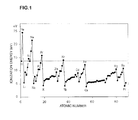
- Fig. 1 is a graph showing the relationship between the atomic number and the ionization energy of elements. As shown in this graph, each of helium, neon, argon, and krypton has a higher ionization energy than that of hydrogen. Among these, helium has the largest ionization energy. In the case where a piezoelectric single-crystal thin film is formed using ions having a large ionization energy, bonds can be efficiently cleaved owing to the release of energy during deionization, thereby efficiently forming the microcavities.
- the density of the implanted rare-gas ions is preferably set from about 2 ⁇ 10 16 to about 5 ⁇ 10 16 atom/cm 2 .
- a density of the implanted rare-gas ions of about 2 ⁇ 10 16 atom/cm 2 results in the generation of microcavities in the separation step to the extent that the single-crystal base composed of the piezoelectric material can be divided at a defective layer in the separation step, resulting in the formation of the single-crystal thin film of the piezoelectric material.
- the density of the implanted rare-gas ions is set about 8 ⁇ 10 16 atom/cm 2 exceeding 5 ⁇ 10 16 atom/cm 2, an excessive amount of microcavities is generated in the defective layer, and the single-crystal base of the piezoelectric material is disadvantageously divided at the defective layer by heat generated in the ion-implantation step. In this case, practical quality cannot be ensured.
- the density of the implanted rare-gas ions is set from about 2 ⁇ 10 16 to about 5 ⁇ 10 16 atom/cm 2 to ensure the practical quality.
- the method for producing a piezoelectric composite substrate further includes a bonding step of bonding a support substrate to be formed into the piezoelectric composite substrate to a surface of the single-crystal base from which the single-crystal thin film is to be detached, in which the bonding step is performed between the ion-implantation step and the separation step.
- the method for producing a piezoelectric composite substrate further includes a planarization step of planarizing a surface of the single-crystal base and a surface of the single-crystal thin film, the surface of the single-crystal base being formed by detaching the single-crystal thin film.
- a method for producing a piezoelectric composite substrate according to a preferred embodiment of the present invention will be described below by taking steps in a method for producing a surface acoustic wave resonator as an example.
- LiNbO 3 is used as a piezoelectric material and a Si substrate is used as a support substrate.
- other materials LiTaO 3 , Li 2 B 4 O 7 , La 3 Ga 5 SiO 14 , and others
- other materials piezoelectric material and other materials (piezoelectric material, glass, and others) may be used as the support substrate.
- Fig. 2 shows a flow chart of the method for producing a surface acoustic wave resonator according to this embodiment.
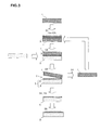
- Fig. 3 is a schematic view showing a piezoelectric composite substrate, a piezoelectric single-crystal base, and a support substrate in steps in the flow chart.
- an ion-implantation step (S1) of implanting He + ions into a mirror-polished main surface of a piezoelectric single-crystal base 1 is performed.
- the implantation energy of He + ions is set to about 150 KeV.
- the dose level (density of implanted ions) is set to about 2 ⁇ 10 16 atom/cm 2 .
- He + ions are accumulated at a depth of about 0.5 ⁇ m below the main surface of the piezoelectric single-crystal base 1 to form microcavities.
- This plane, located at a depth of about 0.5 ⁇ m below the main surface of the piezoelectric single-crystal base 1, is defined as a separation layer 3.
- the crystal orientation of the piezoelectric material affects its electromechanical coefficient, frequency-temperature characteristics, and sound velocity and thus has an important effect on, for example, the frequency, bandwidth, and insertion loss of the surface acoustic wave resonator.
- Appropriate control of the crystal orientation in the vicinity of the main surface of the piezoelectric single-crystal base 1 in this step results in an excellent surface acoustic wave resonator.
- the crystal orientation in the vicinity of the main surface of the piezoelectric single-crystal base 1 can be controlled, resulting in a high degree of design flexibility, e.g., in the frequency, bandwidth, insertion loss, electromechanical coefficient, frequency-temperature characteristics, and sound velocity of a surface acoustic wave resonator to be produced.
- a bonding step (S2) of bonding the main surface of the piezoelectric single-crystal base 1 to a main surface of a support substrate 2 is performed.
- the piezoelectric single-crystal base 1 composed of LiNbO 3 and the support substrate 2 composed of Si are activated with plasma and bonded in vacuo by direct bonding at room temperature.
- a separation step (S3) is performed, the separation step including placing the piezoelectric single-crystal base 1 and the support substrate 2, which have been bonded to each other, in a heated environment with a temperature of about 500°C to divide the separation layer 3.
- the microcavities in the separation layer 3 are grown by thermal stress.
- a portion located from the main surface of the piezoelectric single-crystal base 1 to the separation layer 3, the portion having a thickness of about 0.5 ⁇ m, is detached as a piezoelectric single-crystal thin film 4.
- the piezoelectric single-crystal thin film 4 constitutes a piezoelectric composite substrate 5 together with the support substrate 2.
- the thickness of the piezoelectric single-crystal thin film 4 is determined by the energy of ion implantation.
- the energy of ion implantation can be varied from the value given in the example above, as desired, in order to obtain a selected thickness value for the piezoelectric single-crystal thin film 4.
- the thickness is independent of the undulation of the substrate and is thus stable.
- the sound velocity of a surface acoustic wave is determined by the thickness.
- the production method according to this embodiment therefore, provides a surface acoustic wave resonator with stable performance.
- polishing step (S4) of the separated surface of the remaining piezoelectric single-crystal base 1 and the separated surface of the piezoelectric composite substrate 5 in this example embodiment chemical-mechanical polishing (CMP) is performed.
- CMP chemical-mechanical polishing
- each of the separated surface of the piezoelectric single-crystal base 1 and the separated surface of the piezoelectric composite substrate 5 has roughness about 1 nm as a root-mean-square value (RMS).
- RMS root-mean-square value
- mirror polishing is performed by CMP in such a manner that the roughness becomes less than 1 nm.
- a portion located within about 100 nm from each of the main surfaces in the depth direction is removed.
- the mirror-polished piezoelectric single-crystal base 1 is used again in the ion-implantation step.
- the present invention is not limited to the use of CMP for this polishing step, other suitable techniques may be employed.
- the piezoelectric single-crystal base 1 after mirror polishing is reused; hence, several tens to several hundreds of piezoelectric single-crystal thin films 4 can be provided from the expensive piezoelectric single-crystal base 1, thereby suppressing the amounts of Li, Ta, and the like used per piezoelectric single-crystal thin film 4 and thus suppressing environmental loading. Furthermore, the use of the inexpensive support substrate 2 composed of Si or the like provides the piezoelectric composite substrate 5 at low cost. The reasons the piezoelectric single-crystal base 1 is expensive are that the growing speed of the single crystal is slow, it is difficult to slice the piezoelectric single-crystal base 1 because it breaks easily, and the materials such as Li and Ta are rare materials.
- a polarization step (S5) of polarizing the mirror-polished piezoelectric composite substrate 5 is performed.
- the piezoelectric single-crystal thin film 4 of the piezoelectric composite substrate 5 is subjected to polarization treatment by applying a pulse voltage of about 22 kV and a pulse width of about 5 ms in an environment with a temperature of about 400°C.
- the polarization treatment is performed to repair partial polarization reversal due to the change in electric dipole states in the piezoelectric single crystal by ion implantation and heat treatment.
- the partial polarization reversal is not preferred because it causes a deterioration in piezoelectricity.
- the implementation of this step can recover piezoelectricity.
- the electric dipoles which can be subjected to polarization reversal, in the piezoelectric single crystal are generated by the phenomenon of spontaneous polarization in which electric dipoles generated by allowing positively charged atoms to shift to a negative electrode side and allowing negatively charged atoms to shift to a positive electrode side in an electric field in the crystal remain polarized even when the application of the electric field is stopped.
- the polarization step is desirably performed after the separation step.
- the polarization step is performed at about 200°C to about 1,200°C in view of the melting points of the support substrate and electrodes and the difference in thermal coefficient of expansion.
- a higher temperature results in a reduction in coercive electric field, thereby reducing the applied electric field.
- damage to the crystal due to a direct electric field can be suppressed, which is desirable.
- heating at about 200°C or higher is desirable because the strain in the crystal due to ion implantation is relaxed.
- a heating temperature for relaxing the strain in the crystal may be set to at least about 100°C lower than the Curie temperature in order to avoid disappearance of polarization.
- IDT electrodes that are composed of Al in this example, are formed on the piezoelectric single-crystal thin film 4 of the piezoelectric composite substrate 5 by photolithography to constitute a surface acoustic wave resonator filter.
- the present invention is not limited to the use of Al electrodes, other electrode materials may be used as desired.
- a high power of about 1 to about 2 W is applied.
- Power handling capability of the surface acoustic wave resonator filter is significantly affected by the temperature of an IDT region when an electric signal is applied.
- the IDT region has a high temperature of, for example, about 250°C by applying power, a time until a surface acoustic wave resonator is broken is significantly shortened.
- the increase in the temperature of the IDT region is attributed to the fact that Joule heat due to electrical ohmic loss and heat generation due to elastic sound absorption are not sufficiently dissipated because of the piezoelectric substrate with a low thermal conductivity.
- a surface acoustic wave resonator filter includes a thin film composed of LiTaO 3 or LiNbO 3 having a lower thermal conductivity than that of Si and a support substrate composed of Si having a high thermal conductivity.
- the surface acoustic wave resonator filter has improved heat dissipation properties and thus can withstand high power application.
- the method for producing a surface acoustic wave resonator has been described above. Furthermore, according to preferred embodiments of the present invention, methods for producing a bulk acoustic wave resonator and a boundary acoustic wave resonator can be provided.
- the bulk acoustic wave resonator and the surface acoustic wave resonator may have typical structures.
- the boundary acoustic wave resonator may have a structure disclosed in, for example, Japanese Patent Application No. 2003-32409 .
- He + ions are used as rare-gas ions.
- other rare gas ions may be used. Preferred examples thereof include ions of neon, argon, and krypton, which have a higher ionized energy than that of hydrogen.
- the energy of ion implantation is adapted to the selected type of rare gas ions (as well as to the desired thickness of the piezoelectric single-crystal thin film that becomes detached from the single-crystal base).
Landscapes
- Engineering & Computer Science (AREA)
- Manufacturing & Machinery (AREA)
- Surface Acoustic Wave Elements And Circuit Networks Thereof (AREA)
- Crystals, And After-Treatments Of Crystals (AREA)
- Piezo-Electric Or Mechanical Vibrators, Or Delay Or Filter Circuits (AREA)
Abstract
Description
- The present invention relates to a method for producing a piezoelectric composite substrate having a single-crystal thin film composed of a piezoelectric material.
- In recent years, piezoelectric elements including a piezoelectric composite substrate with a single-crystal thin film composed of a piezoelectric material have been developed. Hitherto, the single-crystal thin film composed of a piezoelectric material has been produced by a first production process including depositing a piezoelectric material, such as AIN or ZnO, using sputtering or CVD (for example, see Y. Osugi et al.; "Single crystal FBAR with LiNbO3 and LiTaO3", 2007 IEEE MTT-S International Microwave Symposium, pp. 873-876) or a second production process including polishing a single-crystal base composed of a piezoelectric material (for example, see M. Bruel; "Silicon on insulator material technology", Electronics Letters, vol. 31, Issue 14, June 6th 1995, p. 1201).
- Alternatively, a third production process is reported, the third production process including implanting helium ions into a Z-cut LiNbO3 substrate to form a damaged crystalline layer and removing the damaged crystalline layer by wet etching to afford a piezoelectric single-crystal thin film (see "Fabrication of single-crystal lithium niobate films by crystal ion slicing", Applied Physics Letters Volume 73, Number 16).
- In the first production process, a deposition temperature and deposition conditions for aligning the orientation direction of the crystal axis of a piezoelectric material place a stringent limitation on materials. Even in the case where an alignment film is provided, the film has a c-axis orientation in which the orientation direction of the crystal axis is aligned vertically to a substrate on which piezoelectric film is disposed. In this case, the orientation direction of the crystal axis cannot be controlled. Thus, the mode of vibration cannot be controlled by slanting the orientation direction of the crystal axis.
- In the second production process, since the single-crystal base composed of the piezoelectric material is polished, most of the piezoelectric material is discarded as shavings, resulting in poor efficiency of utilization of the piezoelectric material. Furthermore, the thickness of the resulting thin film varies depending on the unevenness in polishing speed and the degree of undulation of the base. Thus, it is difficult to control the polishing so as to provide a uniform thickness, leading to poor productivity.
- In the third production process, the use of wet etching increases the production cost. Furthermore, an electrode cannot be provided on a position that can be affected by wet etching. Thus, when the electrode is arranged on a laminating surface between the piezoelectric single-crystal thin film and a support substrate, the electrode is formed after wet etching. In this case, the thin film with a low stiffness is difficult to handle. Thus, it is highly possible that the thin film will be broken.
- Accordingly, to overcome the foregoing problems and form a single-crystal thin film composed of a piezoelectric material, it is an object of the present invention to provide a method for producing a piezoelectric composite substrate.
- According to preferred embodiments of the present invention, a method for producing a piezoelectric composite substrate having a single-crystal thin film composed of a piezoelectric material includes an ion-implantation step and a separation step. In the ion-implantation step, rare-gas ions are implanted into the single-crystal base composed of the piezoelectric material to form localized microcavities in a separation layer located inside the single-crystal base and apart from a surface of the single-crystal base. In the separation step, the microcavities formed in the ion-implantation step are subjected to thermal stress to divide the separation layer of the piezoelectric single-crystal base, thereby detaching the single-crystal thin film.
- In this production method, in the ion-implantation step, the localized microcavities are formed in the separation layer located inside the single-crystal base and apart from the surface of the single-crystal base. In the separation step, the separation layer of the single-crystal base is divided to detach the single-crystal thin film. Thus, the single-crystal base of the piezoelectric material can be reused, thereby increasing efficiency of utilization of the piezoelectric material. Furthermore, the thickness of the thin film is determined by the energy of implantation in the ion-implantation step, thus resulting in the thin film having a uniform thickness. In addition, the mode of vibration can be controlled by regulating the direction of arrangement of the single-crystal base composed of the piezoelectric material to slant the orientation direction of the crystal axis. Moreover, ion implantation has influence on only the separation layer and thus has less influence on the other portion of the piezoelectric composite substrate.
- In the ion-implantation step, rare-gas ions are used. The reason for this is that a rare-gas element has a low reactivity with elements constituting the piezoelectric material compared with other element because the outermost electron orbit of the rare-gas element is filled with electrons. Like a hydrogen-ion implantation employing for the formation of a semiconductor thin film or the like, if ions of an element (including hydrogen) in which the outermost electron orbit is not filled with electrons are used for the production of a thin film of a piezoelectric material, the ions react with elements constituting the piezoelectric material to form stronger bonds. In the case of using hydrogen ions, the bonds are difficult to cut because hydrogen has a low mass, leading to low efficiency of the formation of microcavities. In contrast, in the configuration of using the rare-gas ions according to preferred embodiments of the present invention, the reactivity of the rare-gas ions with the elements constituting the piezoelectric material is lower than that of the above-described ions. Furthermore, the rare-gas ion has a higher mass than that of the hydrogen ion, so that microcavities can be formed efficiently.
- In the ion-implantation step, ions of a rare-gas element having a higher ionization energy than that of hydrogen are preferably used as the rare-gas ions. More preferably, helium ions are used.
-
Fig. 1 is a graph showing the relationship between the atomic number and the ionization energy of elements.
As shown in this graph, each of helium, neon, argon, and krypton has a higher ionization energy than that of hydrogen. Among these, helium has the largest ionization energy. In the case where a piezoelectric single-crystal thin film is formed using ions having a large ionization energy, bonds can be efficiently cleaved owing to the release of energy during deionization, thereby efficiently forming the microcavities. - In the ion-implantation step, the density of the implanted rare-gas ions is preferably set from about 2 × 10¹⁶ to about 5 × 10¹⁶ atom/cm2. A density of the implanted rare-gas ions of about 2 × 10¹⁶ atom/cm2 results in the generation of microcavities in the separation step to the extent that the single-crystal base composed of the piezoelectric material can be divided at a defective layer in the separation step, resulting in the formation of the single-crystal thin film of the piezoelectric material. When a density of the implanted rare-gas ions is set about 8 × 10¹⁶ atom/cm2 exceeding 5 × 10¹⁶ atom/cm2, an excessive amount of microcavities is generated in the defective layer, and the single-crystal base of the piezoelectric material is disadvantageously divided at the defective layer by heat generated in the ion-implantation step. In this case, practical quality cannot be ensured. Thus, the density of the implanted rare-gas ions is set from about 2 × 10¹⁶ to about 5 × 10¹⁶ atom/cm2 to ensure the practical quality.
- Preferably, the method for producing a piezoelectric composite substrate further includes a bonding step of bonding a support substrate to be formed into the piezoelectric composite substrate to a surface of the single-crystal base from which the single-crystal thin film is to be detached, in which the bonding step is performed between the ion-implantation step and the separation step. Preferably, the method for producing a piezoelectric composite substrate further includes a planarization step of planarizing a surface of the single-crystal base and a surface of the single-crystal thin film, the surface of the single-crystal base being formed by detaching the single-crystal thin film.
Other features, elements, characteristics and advantages of the present invention will become more apparent from the following detailed description of preferred embodiments of the present invention with reference to the attached drawings. -
-
Fig. 1 is a graph showing the relationship between the atomic number and the ionization energy of elements; -
Fig. 2 shows a flow chart of a method for producing a surface acoustic wave resonator according to a first embodiment of the present invention; and -
Fig. 3 is a schematic view showing a piezoelectric composite substrate, a piezoelectric single-crystal base, and a support substrate in steps in the flow chart according to the first embodiment of the present invention. - A method for producing a piezoelectric composite substrate according to a preferred embodiment of the present invention will be described below by taking steps in a method for producing a surface acoustic wave resonator as an example. In this embodiment, LiNbO3 is used as a piezoelectric material and a Si substrate is used as a support substrate. However, other materials (LiTaO3, Li2B4O7, La3Ga5SiO14, and others) may be used as the piezoelectric material and other materials (piezoelectric material, glass, and others) may be used as the support substrate.
-
Fig. 2 shows a flow chart of the method for producing a surface acoustic wave resonator according to this embodiment.Fig. 3 is a schematic view showing a piezoelectric composite substrate, a piezoelectric single-crystal base, and a support substrate in steps in the flow chart. - In this production procedure, an ion-implantation step (S1) of implanting He+ ions into a mirror-polished main surface of a piezoelectric single-
crystal base 1 is performed. Here, the implantation energy of He+ ions is set to about 150 KeV. The dose level (density of implanted ions) is set to about 2 × 10¹⁶ atom/cm2. In this case, He+ ions are accumulated at a depth of about 0.5 µm below the main surface of the piezoelectric single-crystal base 1 to form microcavities. This plane, located at a depth of about 0.5 µm below the main surface of the piezoelectric single-crystal base 1, is defined as aseparation layer 3. - In the case of producing a surface acoustic wave resonator, the crystal orientation of the piezoelectric material affects its electromechanical coefficient, frequency-temperature characteristics, and sound velocity and thus has an important effect on, for example, the frequency, bandwidth, and insertion loss of the surface acoustic wave resonator. Appropriate control of the crystal orientation in the vicinity of the main surface of the piezoelectric single-
crystal base 1 in this step results in an excellent surface acoustic wave resonator. In this embodiment, the crystal orientation in the vicinity of the main surface of the piezoelectric single-crystal base 1 can be controlled, resulting in a high degree of design flexibility, e.g., in the frequency, bandwidth, insertion loss, electromechanical coefficient, frequency-temperature characteristics, and sound velocity of a surface acoustic wave resonator to be produced. - A bonding step (S2) of bonding the main surface of the piezoelectric single-
crystal base 1 to a main surface of asupport substrate 2 is performed. Here, there is a difference in coefficient of linear expansion between the piezoelectric single-crystal base 1 composed of LiNbO3 and thesupport substrate 2 composed of Si. Thus, the main surface of the piezoelectric single-crystal base 1 and the main surface of thesupport substrate 2 are activated with plasma and bonded in vacuo by direct bonding at room temperature. - A separation step (S3) is performed, the separation step including placing the piezoelectric single-
crystal base 1 and thesupport substrate 2, which have been bonded to each other, in a heated environment with a temperature of about 500°C to divide theseparation layer 3. In this case, the microcavities in theseparation layer 3 are grown by thermal stress. A portion located from the main surface of the piezoelectric single-crystal base 1 to theseparation layer 3, the portion having a thickness of about 0.5 µm, is detached as a piezoelectric single-crystalthin film 4. The piezoelectric single-crystalthin film 4 constitutes a piezoelectriccomposite substrate 5 together with thesupport substrate 2. - The thickness of the piezoelectric single-crystal
thin film 4 is determined by the energy of ion implantation. Thus, the energy of ion implantation can be varied from the value given in the example above, as desired, in order to obtain a selected thickness value for the piezoelectric single-crystalthin film 4. Unlike polishing, in this method the thickness is independent of the undulation of the substrate and is thus stable. The sound velocity of a surface acoustic wave is determined by the thickness. The production method according to this embodiment, therefore, provides a surface acoustic wave resonator with stable performance. - As polishing step (S4) of the separated surface of the remaining piezoelectric single-
crystal base 1 and the separated surface of the piezoelectriccomposite substrate 5, in this example embodiment chemical-mechanical polishing (CMP) is performed. Here, each of the separated surface of the piezoelectric single-crystal base 1 and the separated surface of the piezoelectriccomposite substrate 5 has roughness about 1 nm as a root-mean-square value (RMS). Thus, mirror polishing is performed by CMP in such a manner that the roughness becomes less than 1 nm. In CMP, a portion located within about 100 nm from each of the main surfaces in the depth direction is removed. The mirror-polished piezoelectric single-crystal base 1 is used again in the ion-implantation step. The present invention is not limited to the use of CMP for this polishing step, other suitable techniques may be employed. - The piezoelectric single-
crystal base 1 after mirror polishing is reused; hence, several tens to several hundreds of piezoelectric single-crystalthin films 4 can be provided from the expensive piezoelectric single-crystal base 1, thereby suppressing the amounts of Li, Ta, and the like used per piezoelectric single-crystalthin film 4 and thus suppressing environmental loading. Furthermore, the use of theinexpensive support substrate 2 composed of Si or the like provides the piezoelectriccomposite substrate 5 at low cost. The reasons the piezoelectric single-crystal base 1 is expensive are that the growing speed of the single crystal is slow, it is difficult to slice the piezoelectric single-crystal base 1 because it breaks easily, and the materials such as Li and Ta are rare materials. - A polarization step (S5) of polarizing the mirror-polished piezoelectric
composite substrate 5 is performed. Here, the piezoelectric single-crystalthin film 4 of the piezoelectriccomposite substrate 5 is subjected to polarization treatment by applying a pulse voltage of about 22 kV and a pulse width of about 5 ms in an environment with a temperature of about 400°C. The polarization treatment is performed to repair partial polarization reversal due to the change in electric dipole states in the piezoelectric single crystal by ion implantation and heat treatment. The partial polarization reversal is not preferred because it causes a deterioration in piezoelectricity. The implementation of this step can recover piezoelectricity. The electric dipoles, which can be subjected to polarization reversal, in the piezoelectric single crystal are generated by the phenomenon of spontaneous polarization in which electric dipoles generated by allowing positively charged atoms to shift to a negative electrode side and allowing negatively charged atoms to shift to a positive electrode side in an electric field in the crystal remain polarized even when the application of the electric field is stopped. - The polarization step is desirably performed after the separation step. The polarization step is performed at about 200°C to about 1,200°C in view of the melting points of the support substrate and electrodes and the difference in thermal coefficient of expansion. A higher temperature results in a reduction in coercive electric field, thereby reducing the applied electric field. In the case where the electric field is intermittently applied for a duration of about 1 µs to about 1 minute, damage to the crystal due to a direct electric field can be suppressed, which is desirable. Furthermore, heating at about 200°C or higher is desirable because the strain in the crystal due to ion implantation is relaxed. A heating temperature for relaxing the strain in the crystal may be set to at least about 100°C lower than the Curie temperature in order to avoid disappearance of polarization.
- As a next step (S6), IDT electrodes, that are composed of Al in this example, are formed on the piezoelectric single-crystal
thin film 4 of the piezoelectriccomposite substrate 5 by photolithography to constitute a surface acoustic wave resonator filter. The present invention is not limited to the use of Al electrodes, other electrode materials may be used as desired. - In the case where a surface acoustic wave resonator filter is used as an RF filter for use in mobile phones, a high power of about 1 to about 2 W is applied. Power handling capability of the surface acoustic wave resonator filter is significantly affected by the temperature of an IDT region when an electric signal is applied. In the case where the IDT region has a high temperature of, for example, about 250°C by applying power, a time until a surface acoustic wave resonator is broken is significantly shortened. The increase in the temperature of the IDT region is attributed to the fact that Joule heat due to electrical ohmic loss and heat generation due to elastic sound absorption are not sufficiently dissipated because of the piezoelectric substrate with a low thermal conductivity. A surface acoustic wave resonator filter according to a preferred embodiment of the present invention includes a thin film composed of LiTaO3 or LiNbO3 having a lower thermal conductivity than that of Si and a support substrate composed of Si having a high thermal conductivity. Thus, the surface acoustic wave resonator filter has improved heat dissipation properties and thus can withstand high power application.
- According to the preferred embodiment of the present invention, the method for producing a surface acoustic wave resonator has been described above. Furthermore, according to preferred embodiments of the present invention, methods for producing a bulk acoustic wave resonator and a boundary acoustic wave resonator can be provided. The bulk acoustic wave resonator and the surface acoustic wave resonator may have typical structures. The boundary acoustic wave resonator may have a structure disclosed in, for example, Japanese Patent Application No.
2003-32409 - In this embodiment, He+ ions are used as rare-gas ions. According to preferred embodiments of the present invention, other rare gas ions may be used. Preferred examples thereof include ions of neon, argon, and krypton, which have a higher ionized energy than that of hydrogen. The energy of ion implantation is adapted to the selected type of rare gas ions (as well as to the desired thickness of the piezoelectric single-crystal thin film that becomes detached from the single-crystal base).
While preferred embodiments of the invention have been described above, it is to be understood that variations and modifications will be apparent to those skilled in the art without departing from the scope and spirit of the invention as defined in the following claims.
Claims (6)
- A method for producing a piezoelectric composite substrate (5) having a single-crystal thin film (4) composed of a piezoelectric material, the method comprising:an ion-implantation step of implanting rare-gas ions into a single-crystal base (1) composed of the piezoelectric material to form localized microcavities in a separation layer (3) located inside the single-crystal base and apart from a surface of the single-crystal base; anda separation step of subjecting the microcavities formed in the ion-implantation step to thermal stress and dividing the separation layer of the single-crystal base to detach the single-crystal thin film (4).
- The method according to Claim 1, wherein in the ion-implantation step, ions of a rare-gas element having a higher ionization energy than that of hydrogen are used as the rare-gas ions.
- The method according to Claim 2, wherein in the ion-implantation step, helium ions are used as the rare-gas ions.
- The method according to any one of Claims 1 to 3, wherein in the ion-implantation step, the density of the implanted rare-gas ions is set to about 2 × 10¹⁶ to about 5 × 10¹⁶ atom/cm2.
- The method according to any one of Claims 1 to 4, further comprising:a bonding step of bonding a support substrate (2) to be formed into the piezoelectric composite substrate (5) to a surface of the single-crystal base (1) from which the single-crystal thin film (4) is to be detached,wherein the bonding step is performed between the ion-implantation step and the separation step.
- The method according to any one of Claims 1 to 5, further comprising:a planarization step of planarizing a surface of the single-crystal base (10 and a surface of the single-crystal thin film (4), the surface of the single-crystal base (1) being formed by detaching the single-crystal thin film (4).
Applications Claiming Priority (1)
| Application Number | Priority Date | Filing Date | Title |
|---|---|---|---|
| JP2008282212A JP4821834B2 (en) | 2008-10-31 | 2008-10-31 | Method for manufacturing piezoelectric composite substrate |
Publications (3)
| Publication Number | Publication Date |
|---|---|
| EP2182562A2 true EP2182562A2 (en) | 2010-05-05 |
| EP2182562A3 EP2182562A3 (en) | 2011-08-31 |
| EP2182562B1 EP2182562B1 (en) | 2013-08-21 |
Family
ID=41697785
Family Applications (1)
| Application Number | Title | Priority Date | Filing Date |
|---|---|---|---|
| EP20090173492 Active EP2182562B1 (en) | 2008-10-31 | 2009-10-20 | Method for producing piezoelectric composite substrate |
Country Status (3)
| Country | Link |
|---|---|
| US (1) | US8932686B2 (en) |
| EP (1) | EP2182562B1 (en) |
| JP (1) | JP4821834B2 (en) |
Cited By (2)
| Publication number | Priority date | Publication date | Assignee | Title |
|---|---|---|---|---|
| WO2017203173A1 (en) * | 2016-05-25 | 2017-11-30 | Soitec | Method for healing defects in a layer obtained by implantation then detachment from a substrate |
| CN113314342A (en) * | 2021-04-15 | 2021-08-27 | 华南师范大学 | Method for improving energy storage density of dielectric film capacitor and dielectric film capacitor |
Families Citing this family (169)
| Publication number | Priority date | Publication date | Assignee | Title |
|---|---|---|---|---|
| JP4582235B2 (en) * | 2008-10-31 | 2010-11-17 | 株式会社村田製作所 | Method for manufacturing piezoelectric device |
| KR101374303B1 (en) * | 2009-11-26 | 2014-03-14 | 가부시키가이샤 무라타 세이사쿠쇼 | Piezoelectric device and method for manufacturing piezoelectric device |
| WO2012043615A1 (en) * | 2010-09-28 | 2012-04-05 | 株式会社村田製作所 | Method for manufacturing piezoelectric device |
| JP5786393B2 (en) * | 2011-03-18 | 2015-09-30 | 株式会社村田製作所 | Quartz device manufacturing method |
| JP5796316B2 (en) * | 2011-03-22 | 2015-10-21 | 株式会社村田製作所 | Method for manufacturing piezoelectric device |
| JP5807715B2 (en) | 2012-03-23 | 2015-11-10 | 株式会社村田製作所 | Elastic wave filter element and manufacturing method thereof |
| JP5934424B2 (en) | 2013-02-19 | 2016-06-15 | 日本碍子株式会社 | Manufacturing method of acoustic wave device |
| JP6170349B2 (en) * | 2013-06-18 | 2017-07-26 | 太陽誘電株式会社 | Elastic wave device |
| JP2017034527A (en) * | 2015-08-04 | 2017-02-09 | セイコーエプソン株式会社 | Piezoelectric element, probe, ultrasonic measurement device, electronic apparatus, polarization treatment method and initialization device |
| FR3042649B1 (en) | 2015-10-20 | 2019-06-21 | Soitec | METHOD FOR MANUFACTURING A HYBRID STRUCTURE |
| FR3054930B1 (en) * | 2016-08-02 | 2018-07-13 | Soitec | USE OF AN ELECTRIC FIELD FOR DETACHING A PIEZOELECTRIC LAYER FROM A DONOR SUBSTRATE |
| KR20180038369A (en) * | 2016-10-06 | 2018-04-16 | 신에쓰 가가꾸 고교 가부시끼가이샤 | Composite substrate manufacturing method |
| CN110249527B (en) * | 2017-02-14 | 2024-01-23 | 京瓷株式会社 | elastic wave element |
| US10911023B2 (en) | 2018-06-15 | 2021-02-02 | Resonant Inc. | Transversely-excited film bulk acoustic resonator with etch-stop layer |
| US11323090B2 (en) | 2018-06-15 | 2022-05-03 | Resonant Inc. | Transversely-excited film bulk acoustic resonator using Y-X-cut lithium niobate for high power applications |
| US12040779B2 (en) | 2020-04-20 | 2024-07-16 | Murata Manufacturing Co., Ltd. | Small transversely-excited film bulk acoustic resonators with enhanced Q-factor |
| US11509279B2 (en) | 2020-07-18 | 2022-11-22 | Resonant Inc. | Acoustic resonators and filters with reduced temperature coefficient of frequency |
| US11206009B2 (en) | 2019-08-28 | 2021-12-21 | Resonant Inc. | Transversely-excited film bulk acoustic resonator with interdigital transducer with varied mark and pitch |
| US10601392B2 (en) | 2018-06-15 | 2020-03-24 | Resonant Inc. | Solidly-mounted transversely-excited film bulk acoustic resonator |
| US10756697B2 (en) | 2018-06-15 | 2020-08-25 | Resonant Inc. | Transversely-excited film bulk acoustic resonator |
| US12237826B2 (en) | 2018-06-15 | 2025-02-25 | Murata Manufacturing Co., Ltd. | Transversely-excited film bulk acoustic resonator with optimized electrode thickness, mark, and pitch |
| US11146232B2 (en) | 2018-06-15 | 2021-10-12 | Resonant Inc. | Transversely-excited film bulk acoustic resonator with reduced spurious modes |
| US11936358B2 (en) | 2020-11-11 | 2024-03-19 | Murata Manufacturing Co., Ltd. | Transversely-excited film bulk acoustic resonator with low thermal impedance |
| US11996827B2 (en) | 2018-06-15 | 2024-05-28 | Murata Manufacturing Co., Ltd. | Transversely-excited film bulk acoustic resonator with periodic etched holes |
| US10637438B2 (en) | 2018-06-15 | 2020-04-28 | Resonant Inc. | Transversely-excited film bulk acoustic resonators for high power applications |
| US11323089B2 (en) | 2018-06-15 | 2022-05-03 | Resonant Inc. | Filter using piezoelectric film bonded to high resistivity silicon substrate with trap-rich layer |
| US10790802B2 (en) | 2018-06-15 | 2020-09-29 | Resonant Inc. | Transversely excited film bulk acoustic resonator using rotated Y-X cut lithium niobate |
| US12088281B2 (en) | 2021-02-03 | 2024-09-10 | Murata Manufacturing Co., Ltd. | Transversely-excited film bulk acoustic resonator with multi-mark interdigital transducer |
| US11323096B2 (en) | 2018-06-15 | 2022-05-03 | Resonant Inc. | Transversely-excited film bulk acoustic resonator with periodic etched holes |
| US11929731B2 (en) | 2018-02-18 | 2024-03-12 | Murata Manufacturing Co., Ltd. | Transversely-excited film bulk acoustic resonator with optimized electrode mark, and pitch |
| US12244295B2 (en) | 2018-06-15 | 2025-03-04 | Murata Manufacturing Co., Ltd. | Transversely-excited film bulk acoustic resonators with two-layer electrodes having a narrower top layer |
| US10868513B2 (en) | 2018-06-15 | 2020-12-15 | Resonant Inc. | Transversely-excited film bulk acoustic filters with symmetric layout |
| US12040781B2 (en) | 2018-06-15 | 2024-07-16 | Murata Manufacturing Co., Ltd. | Transversely-excited film bulk acoustic resonator package |
| US12301212B2 (en) | 2018-06-15 | 2025-05-13 | Murata Manufacturing Co., Ltd. | XBAR resonators with non-rectangular diaphragms |
| US12283944B2 (en) | 2018-06-15 | 2025-04-22 | Murata Manufacturing Co., Ltd. | Transversely-excited film bulk acoustic resonator with recessed rotated-Y-X cut lithium niobate |
| US11201601B2 (en) | 2018-06-15 | 2021-12-14 | Resonant Inc. | Transversely-excited film bulk acoustic resonator with multiple diaphragm thicknesses and fabrication method |
| US12191837B2 (en) | 2018-06-15 | 2025-01-07 | Murata Manufacturing Co., Ltd. | Solidly-mounted transversely-excited film bulk acoustic device |
| US12155374B2 (en) | 2021-04-02 | 2024-11-26 | Murata Manufacturing Co., Ltd. | Tiled transversely-excited film bulk acoustic resonator high power filters |
| US11909381B2 (en) | 2018-06-15 | 2024-02-20 | Murata Manufacturing Co., Ltd. | Transversely-excited film bulk acoustic resonators with two-layer electrodes having a narrower top layer |
| US11146238B2 (en) | 2018-06-15 | 2021-10-12 | Resonant Inc. | Film bulk acoustic resonator fabrication method |
| US10797675B2 (en) | 2018-06-15 | 2020-10-06 | Resonant Inc. | Transversely excited film bulk acoustic resonator using rotated z-cut lithium niobate |
| US10998877B2 (en) | 2018-06-15 | 2021-05-04 | Resonant Inc. | Film bulk acoustic resonator fabrication method with frequency trimming based on electric measurements prior to cavity etch |
| US12170516B2 (en) | 2018-06-15 | 2024-12-17 | Murata Manufacturing Co., Ltd. | Filters using transversly-excited film bulk acoustic resonators with frequency-setting dielectric layers |
| US12021496B2 (en) | 2020-08-31 | 2024-06-25 | Murata Manufacturing Co., Ltd. | Resonators with different membrane thicknesses on the same die |
| US11996825B2 (en) | 2020-06-17 | 2024-05-28 | Murata Manufacturing Co., Ltd. | Filter using lithium niobate and rotated lithium tantalate transversely-excited film bulk acoustic resonators |
| US11264966B2 (en) | 2018-06-15 | 2022-03-01 | Resonant Inc. | Solidly-mounted transversely-excited film bulk acoustic resonator with diamond layers in Bragg reflector stack |
| US11967945B2 (en) | 2018-06-15 | 2024-04-23 | Murata Manufacturing Co., Ltd. | Transversly-excited film bulk acoustic resonators and filters |
| US11876498B2 (en) | 2018-06-15 | 2024-01-16 | Murata Manufacturing Co., Ltd. | Transversely-excited film bulk acoustic resonator with multiple diaphragm thicknesses and fabrication method |
| US11323091B2 (en) | 2018-06-15 | 2022-05-03 | Resonant Inc. | Transversely-excited film bulk acoustic resonator with diaphragm support pedestals |
| US12463619B2 (en) | 2018-06-15 | 2025-11-04 | Murata Manufacturing Co., Ltd. | Filter device |
| US12149227B2 (en) | 2018-06-15 | 2024-11-19 | Murata Manufacturing Co., Ltd. | Transversely-excited film bulk acoustic resonator package |
| US10992284B2 (en) | 2018-06-15 | 2021-04-27 | Resonant Inc. | Filter using transversely-excited film bulk acoustic resonators with multiple frequency setting layers |
| US10985728B2 (en) | 2018-06-15 | 2021-04-20 | Resonant Inc. | Transversely-excited film bulk acoustic resonator and filter with a uniform-thickness dielectric overlayer |
| US12095446B2 (en) | 2018-06-15 | 2024-09-17 | Murata Manufacturing Co., Ltd. | Transversely-excited film bulk acoustic resonator with optimized electrode thickness, mark, and pitch |
| US10998882B2 (en) | 2018-06-15 | 2021-05-04 | Resonant Inc. | XBAR resonators with non-rectangular diaphragms |
| US12009798B2 (en) | 2018-06-15 | 2024-06-11 | Murata Manufacturing Co., Ltd. | Transversely-excited film bulk acoustic resonators with electrodes having irregular hexagon cross-sectional shapes |
| US11171629B2 (en) | 2018-06-15 | 2021-11-09 | Resonant Inc. | Transversely-excited film bulk acoustic resonator using pre-formed cavities |
| US12081187B2 (en) | 2018-06-15 | 2024-09-03 | Murata Manufacturing Co., Ltd. | Transversely-excited film bulk acoustic resonator |
| US12095441B2 (en) | 2018-06-15 | 2024-09-17 | Murata Manufacturing Co., Ltd. | Transversely excited film bulk acoustic resonator with recessed interdigital transducer fingers |
| US12224732B2 (en) | 2018-06-15 | 2025-02-11 | Murata Manufacturing Co., Ltd. | Solidly-mounted transversely-excited film bulk acoustic resonators and filters for 27 GHz communications bands |
| US12218650B2 (en) | 2018-06-15 | 2025-02-04 | Murata Manufacturing Co., Ltd. | Transversely-excited film bulk acoustic resonator |
| US11888463B2 (en) | 2018-06-15 | 2024-01-30 | Murata Manufacturing Co., Ltd. | Multi-port filter using transversely-excited film bulk acoustic resonators |
| US12119808B2 (en) | 2018-06-15 | 2024-10-15 | Murata Manufacturing Co., Ltd. | Transversely-excited film bulk acoustic resonator package |
| US10917072B2 (en) | 2019-06-24 | 2021-02-09 | Resonant Inc. | Split ladder acoustic wave filters |
| US12155371B2 (en) | 2021-03-29 | 2024-11-26 | Murata Manufacturing Co., Ltd. | Layout of xbars with multiple sub-resonators in series |
| US12191838B2 (en) | 2018-06-15 | 2025-01-07 | Murata Manufacturing Co., Ltd. | Solidly-mounted transversely-excited film bulk acoustic device and method |
| US11323095B2 (en) | 2018-06-15 | 2022-05-03 | Resonant Inc. | Rotation in XY plane to suppress spurious modes in XBAR devices |
| US11916539B2 (en) | 2020-02-28 | 2024-02-27 | Murata Manufacturing Co., Ltd. | Split-ladder band N77 filter using transversely-excited film bulk acoustic resonators |
| US12113512B2 (en) | 2021-03-29 | 2024-10-08 | Murata Manufacturing Co., Ltd. | Layout of XBARs with multiple sub-resonators in parallel |
| US11949402B2 (en) | 2020-08-31 | 2024-04-02 | Murata Manufacturing Co., Ltd. | Resonators with different membrane thicknesses on the same die |
| US11374549B2 (en) | 2018-06-15 | 2022-06-28 | Resonant Inc. | Filter using transversely-excited film bulk acoustic resonators with divided frequency-setting dielectric layers |
| US11728785B2 (en) | 2018-06-15 | 2023-08-15 | Murata Manufacturing Co., Ltd. | Transversely-excited film bulk acoustic resonator using pre-formed cavities |
| US12212306B2 (en) | 2018-06-15 | 2025-01-28 | Murata Manufacturing Co., Ltd. | Transversely-excited film bulk acoustic resonator with multiple diaphragm thicknesses and fabrication method |
| US10819309B1 (en) | 2019-04-05 | 2020-10-27 | Resonant Inc. | Transversely-excited film bulk acoustic resonator package and method |
| US12184261B2 (en) | 2018-06-15 | 2024-12-31 | Murata Manufacturing Co., Ltd. | Transversely-excited film bulk acoustic resonator with a cavity having round end zones |
| US11870423B2 (en) | 2018-06-15 | 2024-01-09 | Murata Manufacturing Co., Ltd. | Wide bandwidth temperature-compensated transversely-excited film bulk acoustic resonator |
| US11228296B2 (en) | 2018-06-15 | 2022-01-18 | Resonant Inc. | Transversely-excited film bulk acoustic resonator with a cavity having a curved perimeter |
| US11349450B2 (en) | 2018-06-15 | 2022-05-31 | Resonant Inc. | Symmetric transversely-excited film bulk acoustic resonators with reduced spurious modes |
| US10992283B2 (en) | 2018-06-15 | 2021-04-27 | Resonant Inc. | High power transversely-excited film bulk acoustic resonators on rotated Z-cut lithium niobate |
| US11329628B2 (en) | 2020-06-17 | 2022-05-10 | Resonant Inc. | Filter using lithium niobate and lithium tantalate transversely-excited film bulk acoustic resonators |
| US12237827B2 (en) | 2018-06-15 | 2025-02-25 | Murata Manufacturing Co., Ltd. | Solidly-mounted transversely-excited film bulk acoustic filters with multiple piezoelectric plate thicknesses |
| US12119805B2 (en) | 2018-06-15 | 2024-10-15 | Murata Manufacturing Co., Ltd. | Substrate processing and membrane release of transversely-excited film bulk acoustic resonator using a sacrificial tub |
| US10826462B2 (en) | 2018-06-15 | 2020-11-03 | Resonant Inc. | Transversely-excited film bulk acoustic resonators with molybdenum conductors |
| US12375056B2 (en) | 2018-06-15 | 2025-07-29 | Murata Manufacturing Co., Ltd. | Transversely-excited film bulk acoustic resonators |
| US11349452B2 (en) | 2018-06-15 | 2022-05-31 | Resonant Inc. | Transversely-excited film bulk acoustic filters with symmetric layout |
| US11996822B2 (en) | 2018-06-15 | 2024-05-28 | Murata Manufacturing Co., Ltd. | Wide bandwidth time division duplex transceiver |
| US11901878B2 (en) | 2018-06-15 | 2024-02-13 | Murata Manufacturing Co., Ltd. | Transversely-excited film bulk acoustic resonators with two-layer electrodes with a wider top layer |
| JP7127472B2 (en) * | 2018-10-15 | 2022-08-30 | 日本電信電話株式会社 | Manufacturing method of wavelength conversion element |
| DE112019005403T5 (en) | 2018-10-31 | 2021-07-15 | Resonant Inc. | FIXED MOUNTED TRANSVERSAL EXCITED ACOUSTIC FILM VOLUME RESONATOR |
| CN109818590B (en) * | 2019-03-13 | 2021-12-03 | 电子科技大学 | Single crystal film preparation method with stress buffer layer, single crystal film and resonator |
| US11901873B2 (en) | 2019-03-14 | 2024-02-13 | Murata Manufacturing Co., Ltd. | Transversely-excited film bulk acoustic resonator with partial BRAGG reflectors |
| CN113615083B (en) | 2019-03-14 | 2024-10-15 | 株式会社村田制作所 | Laterally excited film bulk acoustic resonator with half-λ dielectric layer |
| US10911021B2 (en) | 2019-06-27 | 2021-02-02 | Resonant Inc. | Transversely-excited film bulk acoustic resonator with lateral etch stop |
| US12034423B2 (en) | 2019-06-27 | 2024-07-09 | Murata Manufacturing Co., Ltd | XBAR frontside etch process using polysilicon sacrificial layer |
| US11329625B2 (en) | 2019-07-18 | 2022-05-10 | Resonant Inc. | Film bulk acoustic sensors using thin LN-LT layer |
| US10862454B1 (en) | 2019-07-18 | 2020-12-08 | Resonant Inc. | Film bulk acoustic resonators in thin LN-LT layers |
| US12506462B2 (en) | 2020-02-28 | 2025-12-23 | Murata Manufacturing Co., Ltd. | Transversely-excited film bulk acoustic resonator with multi-pitch interdigital transducer |
| US12255625B2 (en) | 2020-02-28 | 2025-03-18 | Murata Manufacturing Co., Ltd. | Filter using transversely-excited film bulk acoustic resonators with inductively coupled sub-resonators |
| CN111341904B (en) * | 2020-03-04 | 2023-06-23 | 济南晶正电子科技有限公司 | Piezoelectric film, preparation method thereof and method for determining direction of piezoelectric crystal axis |
| US12278617B2 (en) | 2020-04-20 | 2025-04-15 | Murata Manufacturing Co., Ltd. | High Q solidly-mounted transversely-excited film bulk acoustic resonators |
| US12341493B2 (en) | 2020-04-20 | 2025-06-24 | Murata Manufacturing Co., Ltd. | Low loss transversely-excited film bulk acoustic resonators and filters |
| US12341490B2 (en) | 2020-04-20 | 2025-06-24 | Murata Manufacturing Co., Ltd. | Low loss transversely-excited film bulk acoustic resonators and filters |
| US11811391B2 (en) | 2020-05-04 | 2023-11-07 | Murata Manufacturing Co., Ltd. | Transversely-excited film bulk acoustic resonator with etched conductor patterns |
| US11469733B2 (en) | 2020-05-06 | 2022-10-11 | Resonant Inc. | Transversely-excited film bulk acoustic resonators with interdigital transducer configured to reduce diaphragm stress |
| JP7402112B2 (en) * | 2020-05-08 | 2023-12-20 | 信越化学工業株式会社 | Method for manufacturing composite substrate with piezoelectric single crystal film |
| US12074584B2 (en) | 2020-05-28 | 2024-08-27 | Murata Manufacturing Co., Ltd. | Transversely-excited film bulk acoustic resonators with two-layer electrodes |
| US12267062B2 (en) | 2020-06-17 | 2025-04-01 | Murata Manufacturing Co., Ltd. | Transversely-excited film bulk acoustic resonators with three-layer electrodes |
| US10992282B1 (en) | 2020-06-18 | 2021-04-27 | Resonant Inc. | Transversely-excited film bulk acoustic resonators with electrodes having a second layer of variable width |
| CN111834519B (en) * | 2020-06-29 | 2021-12-03 | 中国科学院上海微系统与信息技术研究所 | Method for improving thickness uniformity of single crystal piezoelectric film |
| US11742828B2 (en) | 2020-06-30 | 2023-08-29 | Murata Manufacturing Co., Ltd. | Transversely-excited film bulk acoustic resonator with symmetric diaphragm |
| US11482981B2 (en) | 2020-07-09 | 2022-10-25 | Resonanat Inc. | Transversely-excited film bulk acoustic resonators with piezoelectric diaphragm supported by piezoelectric substrate |
| US11264969B1 (en) | 2020-08-06 | 2022-03-01 | Resonant Inc. | Transversely-excited film bulk acoustic resonator comprising small cells |
| US11671070B2 (en) | 2020-08-19 | 2023-06-06 | Murata Manufacturing Co., Ltd. | Transversely-excited film bulk acoustic resonators using multiple dielectric layer thicknesses to suppress spurious modes |
| US11271539B1 (en) | 2020-08-19 | 2022-03-08 | Resonant Inc. | Transversely-excited film bulk acoustic resonator with tether-supported diaphragm |
| US11894835B2 (en) | 2020-09-21 | 2024-02-06 | Murata Manufacturing Co., Ltd. | Sandwiched XBAR for third harmonic operation |
| US11929733B2 (en) | 2020-10-05 | 2024-03-12 | Murata Manufacturing Co., Ltd. | Transversely-excited film bulk acoustic resonator matrix filters with input and output impedances matched to radio frequency front end elements |
| US11405017B2 (en) | 2020-10-05 | 2022-08-02 | Resonant Inc. | Acoustic matrix filters and radios using acoustic matrix filters |
| US11405019B2 (en) | 2020-10-05 | 2022-08-02 | Resonant Inc. | Transversely-excited film bulk acoustic resonator matrix filters |
| US11728784B2 (en) | 2020-10-05 | 2023-08-15 | Murata Manufacturing Co., Ltd. | Transversely-excited film bulk acoustic resonator matrix filters with split die sub-filters |
| US11658639B2 (en) | 2020-10-05 | 2023-05-23 | Murata Manufacturing Co., Ltd. | Transversely-excited film bulk acoustic resonator matrix filters with noncontiguous passband |
| US11476834B2 (en) | 2020-10-05 | 2022-10-18 | Resonant Inc. | Transversely-excited film bulk acoustic resonator matrix filters with switches in parallel with sub-filter shunt capacitors |
| US11463066B2 (en) | 2020-10-14 | 2022-10-04 | Resonant Inc. | Transversely-excited film bulk acoustic resonators with piezoelectric diaphragm supported by piezoelectric substrate |
| US12119806B2 (en) | 2020-10-30 | 2024-10-15 | Murata Manufacturing Co., Ltd. | Transversely-excited film bulk acoustic resonator with spiral interdigitated transducer fingers |
| US12003226B2 (en) | 2020-11-11 | 2024-06-04 | Murata Manufacturing Co., Ltd | Transversely-excited film bulk acoustic resonator with low thermal impedance |
| US12255617B2 (en) | 2020-11-11 | 2025-03-18 | Murata Manufacturing Co., Ltd. | Solidly-mounted transversely-excited film bulk acoustic resonators with low thermal impedance |
| US12431856B2 (en) | 2020-11-12 | 2025-09-30 | Murata Manufacturing Co., Ltd. | Transversely-excited film bulk acoustic resonator with reduced loss in the aperture direction |
| US11496113B2 (en) | 2020-11-13 | 2022-11-08 | Resonant Inc. | XBAR devices with excess piezoelectric material removed |
| US12255626B2 (en) | 2020-11-13 | 2025-03-18 | Murata Manufacturing Co., Ltd. | Solidly-mounted transversely-excited film bulk acoustic filters with excess piezoelectric material removed |
| US12362725B2 (en) | 2020-11-13 | 2025-07-15 | Murata Manufacturing Co., Ltd. | Transversely-excited film bulk acoustic filters with excess piezoelectric material removed |
| US12028039B2 (en) | 2020-11-13 | 2024-07-02 | Murata Manufacturing Co., Ltd. | Forming XBAR devices with excess piezoelectric material removed |
| US11405020B2 (en) | 2020-11-26 | 2022-08-02 | Resonant Inc. | Transversely-excited film bulk acoustic resonators with structures to reduce acoustic energy leakage |
| FR3116652A1 (en) * | 2020-11-26 | 2022-05-27 | Commissariat A L'energie Atomique Et Aux Energies Alternatives | Process for manufacturing a component comprising a layer of monocrystalline material compatible with high thermal budgets |
| US12166468B2 (en) | 2021-01-15 | 2024-12-10 | Murata Manufacturing Co., Ltd. | Decoupled transversely-excited film bulk acoustic resonators for high power filters |
| US12126318B2 (en) | 2021-01-15 | 2024-10-22 | Murata Manufacturing Co., Ltd. | Filters using decoupled transversely-excited film bulk acoustic resonators |
| US11239816B1 (en) | 2021-01-15 | 2022-02-01 | Resonant Inc. | Decoupled transversely-excited film bulk acoustic resonators |
| US12463615B2 (en) | 2021-01-21 | 2025-11-04 | Murata Manufacturing Co., Ltd | Transversely-excited film bulk acoustic resonators with improved coupling and reduced energy leakage |
| US12308826B2 (en) | 2021-02-03 | 2025-05-20 | Murata Manufacturing Co., Ltd. | Bandpass filters using transversely-excited film bulk acoustic resonators |
| US12113510B2 (en) | 2021-02-03 | 2024-10-08 | Murata Manufacturing Co., Ltd. | Transversely-excited film bulk acoustic resonators with multiple piezoelectric membrane thicknesses on the same chip |
| US12308825B2 (en) | 2021-02-12 | 2025-05-20 | Murata Manufacturing Co., Ltd | Transversely-excited film bulk acoustic resonators with narrow gaps between busbars and ends of interdigital transducer fingers |
| US12355426B2 (en) | 2021-03-24 | 2025-07-08 | Murata Manufacturing Co., Ltd. | Acoustic filters with shared acoustic tracks |
| US12348216B2 (en) | 2021-03-24 | 2025-07-01 | Murata Manufacturing Co., Ltd. | Acoustic filters with shared acoustic tracks and cascaded series resonators |
| US12126328B2 (en) | 2021-03-24 | 2024-10-22 | Murata Manufacturing Co., Ltd. | Acoustic filters with shared acoustic tracks |
| US12289099B2 (en) | 2021-03-24 | 2025-04-29 | Murata Manufacturing Co., Ltd. | Acoustic filters with shared acoustic tracks for series and shunt resonators |
| US12341492B2 (en) | 2021-03-29 | 2025-06-24 | Murata Manufacturing Co., Ltd. | Transversely-excited film bulk acoustic resonators with busbar side edges that form angles with a perimeter of the cavity |
| CN120454674A (en) | 2021-03-30 | 2025-08-08 | 株式会社村田制作所 | Filter for 6 GHz Wi-Fi using laterally excited film bulk acoustic resonators |
| US12224735B2 (en) | 2021-03-30 | 2025-02-11 | Murata Manufacturing Co., Ltd. | Diplexer using decoupled transversely-excited film bulk acoustic resonators |
| US12237823B2 (en) | 2021-04-02 | 2025-02-25 | Murata Manufacturing Co., Ltd. | Transversely-excited film bulk acoustic resonators with solidly mounted resonator (SMR) pedestals |
| US12249971B2 (en) | 2021-04-02 | 2025-03-11 | Murata Manufacturing Co., Ltd. | Transversely-excited film bulk acoustic resonators with solidly mounted resonator (SMR) pedestals |
| US12255633B2 (en) | 2021-04-16 | 2025-03-18 | Murata Manufacturing Co., Ltd. | Filter using transversely-excited film bulk acoustic resonators |
| US12126316B2 (en) | 2021-04-16 | 2024-10-22 | Murata Manufacturing Co., Ltd | Transversely-excited film bulk acoustic resonator |
| US12160220B2 (en) | 2021-04-30 | 2024-12-03 | Murata Manufacturing Co., Ltd. | Transversely-excited film bulk acoustic resonator with oxide strip acoustic confinement structures |
| US12255607B2 (en) | 2021-04-30 | 2025-03-18 | Murata Manufacturing Co., Ltd. | Transversely-excited film bulk acoustic resonator with buried oxide strip acoustic confinement structures |
| US12075700B2 (en) | 2021-05-07 | 2024-08-27 | Murata Manufacturing Co., Ltd. | Transversely-excited film bulk acoustic resonator fabrication using polysilicon pillars |
| US12057823B2 (en) | 2021-05-07 | 2024-08-06 | Murata Manufacturing Co., Ltd. | Transversely-excited film bulk acoustic resonator with concentric interdigitated transducer fingers |
| US12170513B2 (en) | 2021-06-30 | 2024-12-17 | Murata Manufacturing Co., Ltd. | Transversely-excited film bulk acoustic resonator with reduced substrate to contact bump thermal resistance |
| US12603639B2 (en) | 2021-08-02 | 2026-04-14 | Murata Manufacturing Co., Ltd. | Metal cavity for transversely-excited film bulk acoustic resonator (XBAR) |
| US12456962B2 (en) | 2021-09-24 | 2025-10-28 | Murata Manufacturing Co., Ltd. | Transversely-excited film bulk acoustic resonators wafer-level packaging using a dielectric cover |
| US12451864B2 (en) | 2021-09-29 | 2025-10-21 | Murata Manufacturing Co., Ltd. | Transversely-excited film bulk acoustic resonators with curved shaped ends of fingers or opposing busbars |
| US12225387B2 (en) | 2021-09-29 | 2025-02-11 | Murata Manufacturing Co., Ltd. | Communications device with concurrent operation in 5GHZ and 6GHZ U-NII frequency ranges |
| US12407326B2 (en) | 2021-11-04 | 2025-09-02 | Murata Manufacturing Co., Ltd. | Stacked die transversely-excited film bulk acoustic resonator (XBAR) filters |
| US12424999B2 (en) | 2021-12-28 | 2025-09-23 | Murata Manufacturing Co., Ltd. | Transversely-excited film bulk acoustic resonators with gap dielectric stripes in busbar-electrode gaps |
| US12494768B2 (en) | 2021-12-28 | 2025-12-09 | Murata Manufacturing Co., Ltd. | Transversely-excited film bulk acoustic resonators with gap dielectric stripes in busbar-electrode gaps |
| US12413196B2 (en) | 2022-02-16 | 2025-09-09 | Murata Manufacturing Co., Ltd. | Tuning acoustic resonators with back-side coating |
| US12489417B2 (en) | 2022-04-12 | 2025-12-02 | Murata Manufacturing Co., Ltd. | Ladder filter with transversely-excited film bulk acoustic resonators having different pitches |
| US12549151B2 (en) | 2022-04-12 | 2026-02-10 | Murata Manufacturing Co., Ltd. | Transversely-excited film bulk acoustic resonator with thick dielectric layer for improved coupling |
| US12489415B2 (en) | 2022-10-19 | 2025-12-02 | Murata Manufacturing Co., Ltd. | Acoustic resonator lid for thermal transport |
| CN116482880A (en) * | 2023-04-26 | 2023-07-25 | 湖北九峰山实验室 | Silicon-based micro-ring resonant wavelength control device and manufacturing method thereof |
| FR3157060A1 (en) * | 2023-12-19 | 2025-06-20 | Soitec | Regeneration of a donor substrate for the fabrication of a POI structure |
| CN118946239A (en) * | 2024-06-28 | 2024-11-12 | 泉州市三安集成电路有限公司 | A piezoelectric substrate manufacturing method, composite substrate and elastic wave device |
Citations (1)
| Publication number | Priority date | Publication date | Assignee | Title |
|---|---|---|---|---|
| JP2003032409A (en) | 2001-07-13 | 2003-01-31 | Konica Corp | Image data processing system |
Family Cites Families (11)
| Publication number | Priority date | Publication date | Assignee | Title |
|---|---|---|---|---|
| JP3257624B2 (en) * | 1996-11-15 | 2002-02-18 | キヤノン株式会社 | Semiconductor member manufacturing method |
| SG65697A1 (en) | 1996-11-15 | 1999-06-22 | Canon Kk | Process for producing semiconductor article |
| JP3880150B2 (en) * | 1997-06-02 | 2007-02-14 | 松下電器産業株式会社 | Surface acoustic wave device |
| US6120597A (en) * | 1998-02-17 | 2000-09-19 | The Trustees Of Columbia University In The City Of New York | Crystal ion-slicing of single-crystal films |
| US6641662B2 (en) | 1998-02-17 | 2003-11-04 | The Trustees Of Columbia University In The City Of New York | Method for fabricating ultra thin single-crystal metal oxide wave retarder plates and waveguide polarization mode converter using the same |
| FR2788176B1 (en) | 1998-12-30 | 2001-05-25 | Thomson Csf | GUIDED ACOUSTIC WAVE DEVICE IN A THIN LAYER OF PIEZOELECTRIC MATERIAL ADHESED BY A MOLECULAR ADHESIVE ONTO A CARRIER SUBSTRATE AND MANUFACTURING METHOD |
| JP2003017967A (en) * | 2001-06-29 | 2003-01-17 | Toshiba Corp | Surface acoustic wave device and method of manufacturing the same |
| JP2003095798A (en) * | 2001-09-27 | 2003-04-03 | Hoya Corp | Manufacturing method of single crystal substrate |
| US6777727B2 (en) * | 2002-11-26 | 2004-08-17 | Motorola, Inc. | Flexural plate wave systems |
| JP2005093898A (en) * | 2003-09-19 | 2005-04-07 | Sanyo Electric Co Ltd | Crystal substrate and device manufacturing method |
| FR2914492A1 (en) * | 2007-03-27 | 2008-10-03 | Soitec Silicon On Insulator | Substrate's thin ferroelectric layer manufacturing method for manufacturing e.g. piezoelectric sensor, involves subjecting resulting structure having transferred thin layer to electrical field to improve ferroelectric properties of layer |
-
2008
- 2008-10-31 JP JP2008282212A patent/JP4821834B2/en active Active
-
2009
- 2009-10-20 EP EP20090173492 patent/EP2182562B1/en active Active
- 2009-10-29 US US12/608,120 patent/US8932686B2/en active Active
Patent Citations (1)
| Publication number | Priority date | Publication date | Assignee | Title |
|---|---|---|---|---|
| JP2003032409A (en) | 2001-07-13 | 2003-01-31 | Konica Corp | Image data processing system |
Non-Patent Citations (3)
| Title |
|---|
| "Fabrication of single-crystal lithium niobate films by crystal ion slicing", APPLIED PHYSICS LETTERS, vol. 73, no. 16 |
| M. BRUEL: "Silicon on insulator material technology", ELECTRONICS LETTERS, vol. 31, no. 14, 6 June 1995 (1995-06-06), pages 1201 |
| Y. OSUGI ET AL.: "Single crystal FBAR with LiNb03 and LiTa03", IEEE MTT-S INTERNATIONAL MICROWAVE SYMPOSIUM, 2007, pages 873 - 876 |
Cited By (7)
| Publication number | Priority date | Publication date | Assignee | Title |
|---|---|---|---|---|
| WO2017203173A1 (en) * | 2016-05-25 | 2017-11-30 | Soitec | Method for healing defects in a layer obtained by implantation then detachment from a substrate |
| FR3051979A1 (en) * | 2016-05-25 | 2017-12-01 | Soitec Silicon On Insulator | METHOD FOR THE HEALING OF DEFECTS IN A LAYER OBTAINED BY IMPLANTATION AND DETACHMENT OF A SUBSTRATE |
| CN109155358A (en) * | 2016-05-25 | 2019-01-04 | 索泰克公司 | For repairing the method for then separating the defects of layer obtained with substrate by injection |
| KR20190013896A (en) * | 2016-05-25 | 2019-02-11 | 소이텍 | Methods of healing defects in the layer obtained by implantation and separation from the substrate |
| CN109155358B (en) * | 2016-05-25 | 2022-06-03 | 索泰克公司 | Method for repairing defects in a layer obtained by implantation and then detachment from a substrate |
| CN113314342A (en) * | 2021-04-15 | 2021-08-27 | 华南师范大学 | Method for improving energy storage density of dielectric film capacitor and dielectric film capacitor |
| CN113314342B (en) * | 2021-04-15 | 2022-08-05 | 华南师范大学 | Method for improving energy storage density of dielectric film capacitor and dielectric film capacitor |
Also Published As
| Publication number | Publication date |
|---|---|
| US8932686B2 (en) | 2015-01-13 |
| US20100108248A1 (en) | 2010-05-06 |
| JP2010109909A (en) | 2010-05-13 |
| JP4821834B2 (en) | 2011-11-24 |
| EP2182562B1 (en) | 2013-08-21 |
| EP2182562A3 (en) | 2011-08-31 |
Similar Documents
| Publication | Publication Date | Title |
|---|---|---|
| EP2182562B1 (en) | Method for producing piezoelectric composite substrate | |
| US9385301B2 (en) | Method for manufacturing composite piezoelectric substrate | |
| US8572825B2 (en) | Method for producing piezoelectric composite substrate and method for producing piezoelectric element | |
| EP2182561B1 (en) | Method for manufacturing electronic device and method for manufacturing piezoelectric device | |
| US9246462B2 (en) | Method for manufacturing piezoelectric device | |
| EP2690782B1 (en) | Piezoelectric device and manufacturing method for piezoelectric device | |
| JP2003017967A (en) | Surface acoustic wave device and method of manufacturing the same | |
| JP5359615B2 (en) | Manufacturing method of composite substrate | |
| CN108603305A (en) | Method for producing single crystal layer, especially piezoelectric layer | |
| WO2012043616A1 (en) | Piezoelectric device and method for manufacturing piezoelectric device | |
| JP2019506043A (en) | Substrates for temperature compensated surface acoustic wave devices or bulk acoustic wave devices | |
| JP5277975B2 (en) | Manufacturing method of composite substrate | |
| CN117460388B (en) | Composite substrate and preparation method thereof | |
| WO2011074329A1 (en) | Method for manufacturing piezoelectric device | |
| KR102870817B1 (en) | A process for manufacturing a piezoelectric structure for a radio frequency device, which can be used to transfer a piezoelectric layer, and a process for transferring such a piezoelectric layer |
Legal Events
| Date | Code | Title | Description |
|---|---|---|---|
| PUAI | Public reference made under article 153(3) epc to a published international application that has entered the european phase |
Free format text: ORIGINAL CODE: 0009012 |
|
| AK | Designated contracting states |
Kind code of ref document: A2 Designated state(s): AT BE BG CH CY CZ DE DK EE ES FI FR GB GR HR HU IE IS IT LI LT LU LV MC MK MT NL NO PL PT RO SE SI SK SM TR |
|
| AX | Request for extension of the european patent |
Extension state: AL BA RS |
|
| PUAL | Search report despatched |
Free format text: ORIGINAL CODE: 0009013 |
|
| AK | Designated contracting states |
Kind code of ref document: A3 Designated state(s): AT BE BG CH CY CZ DE DK EE ES FI FR GB GR HR HU IE IS IT LI LT LU LV MC MK MT NL NO PL PT RO SE SI SK SM TR |
|
| AX | Request for extension of the european patent |
Extension state: AL BA RS |
|
| RIC1 | Information provided on ipc code assigned before grant |
Ipc: H01L 41/22 20060101AFI20110728BHEP |
|
| 17P | Request for examination filed |
Effective date: 20120229 |
|
| 17Q | First examination report despatched |
Effective date: 20120718 |
|
| REG | Reference to a national code |
Ref country code: DE Ref legal event code: R079 Ref document number: 602009018138 Country of ref document: DE Free format text: PREVIOUS MAIN CLASS: H01L0041220000 Ipc: H01L0041312000 |
|
| GRAP | Despatch of communication of intention to grant a patent |
Free format text: ORIGINAL CODE: EPIDOSNIGR1 |
|
| RIC1 | Information provided on ipc code assigned before grant |
Ipc: H01L 41/312 20130101AFI20130219BHEP |
|
| INTG | Intention to grant announced |
Effective date: 20130325 |
|
| RIN1 | Information on inventor provided before grant (corrected) |
Inventor name: HAYAKAWA, NORIHIRO Inventor name: IWAMOTO, TAKASHI Inventor name: KANDO, HAJIME |
|
| GRAS | Grant fee paid |
Free format text: ORIGINAL CODE: EPIDOSNIGR3 |
|
| GRAA | (expected) grant |
Free format text: ORIGINAL CODE: 0009210 |
|
| AK | Designated contracting states |
Kind code of ref document: B1 Designated state(s): AT BE BG CH CY CZ DE DK EE ES FI FR GB GR HR HU IE IS IT LI LT LU LV MC MK MT NL NO PL PT RO SE SI SK SM TR |
|
| REG | Reference to a national code |
Ref country code: GB Ref legal event code: FG4D |
|
| REG | Reference to a national code |
Ref country code: CH Ref legal event code: EP |
|
| REG | Reference to a national code |
Ref country code: AT Ref legal event code: REF Ref document number: 628546 Country of ref document: AT Kind code of ref document: T Effective date: 20130915 |
|
| REG | Reference to a national code |
Ref country code: IE Ref legal event code: FG4D |
|
| REG | Reference to a national code |
Ref country code: DE Ref legal event code: R096 Ref document number: 602009018138 Country of ref document: DE Effective date: 20131017 |
|
| REG | Reference to a national code |
Ref country code: AT Ref legal event code: MK05 Ref document number: 628546 Country of ref document: AT Kind code of ref document: T Effective date: 20130821 Ref country code: NL Ref legal event code: VDEP Effective date: 20130821 |
|
| REG | Reference to a national code |
Ref country code: LT Ref legal event code: MG4D |
|
| PG25 | Lapsed in a contracting state [announced via postgrant information from national office to epo] |
Ref country code: NO Free format text: LAPSE BECAUSE OF FAILURE TO SUBMIT A TRANSLATION OF THE DESCRIPTION OR TO PAY THE FEE WITHIN THE PRESCRIBED TIME-LIMIT Effective date: 20131121 Ref country code: CY Free format text: LAPSE BECAUSE OF FAILURE TO SUBMIT A TRANSLATION OF THE DESCRIPTION OR TO PAY THE FEE WITHIN THE PRESCRIBED TIME-LIMIT Effective date: 20130828 Ref country code: PT Free format text: LAPSE BECAUSE OF FAILURE TO SUBMIT A TRANSLATION OF THE DESCRIPTION OR TO PAY THE FEE WITHIN THE PRESCRIBED TIME-LIMIT Effective date: 20131223 Ref country code: IS Free format text: LAPSE BECAUSE OF FAILURE TO SUBMIT A TRANSLATION OF THE DESCRIPTION OR TO PAY THE FEE WITHIN THE PRESCRIBED TIME-LIMIT Effective date: 20131221 Ref country code: AT Free format text: LAPSE BECAUSE OF FAILURE TO SUBMIT A TRANSLATION OF THE DESCRIPTION OR TO PAY THE FEE WITHIN THE PRESCRIBED TIME-LIMIT Effective date: 20130821 Ref country code: LT Free format text: LAPSE BECAUSE OF FAILURE TO SUBMIT A TRANSLATION OF THE DESCRIPTION OR TO PAY THE FEE WITHIN THE PRESCRIBED TIME-LIMIT Effective date: 20130821 Ref country code: HR Free format text: LAPSE BECAUSE OF FAILURE TO SUBMIT A TRANSLATION OF THE DESCRIPTION OR TO PAY THE FEE WITHIN THE PRESCRIBED TIME-LIMIT Effective date: 20130821 Ref country code: SE Free format text: LAPSE BECAUSE OF FAILURE TO SUBMIT A TRANSLATION OF THE DESCRIPTION OR TO PAY THE FEE WITHIN THE PRESCRIBED TIME-LIMIT Effective date: 20130821 |
|
| PG25 | Lapsed in a contracting state [announced via postgrant information from national office to epo] |
Ref country code: LV Free format text: LAPSE BECAUSE OF FAILURE TO SUBMIT A TRANSLATION OF THE DESCRIPTION OR TO PAY THE FEE WITHIN THE PRESCRIBED TIME-LIMIT Effective date: 20130821 Ref country code: BE Free format text: LAPSE BECAUSE OF FAILURE TO SUBMIT A TRANSLATION OF THE DESCRIPTION OR TO PAY THE FEE WITHIN THE PRESCRIBED TIME-LIMIT Effective date: 20130821 Ref country code: PL Free format text: LAPSE BECAUSE OF FAILURE TO SUBMIT A TRANSLATION OF THE DESCRIPTION OR TO PAY THE FEE WITHIN THE PRESCRIBED TIME-LIMIT Effective date: 20130821 Ref country code: FI Free format text: LAPSE BECAUSE OF FAILURE TO SUBMIT A TRANSLATION OF THE DESCRIPTION OR TO PAY THE FEE WITHIN THE PRESCRIBED TIME-LIMIT Effective date: 20130821 Ref country code: GR Free format text: LAPSE BECAUSE OF FAILURE TO SUBMIT A TRANSLATION OF THE DESCRIPTION OR TO PAY THE FEE WITHIN THE PRESCRIBED TIME-LIMIT Effective date: 20131122 Ref country code: SI Free format text: LAPSE BECAUSE OF FAILURE TO SUBMIT A TRANSLATION OF THE DESCRIPTION OR TO PAY THE FEE WITHIN THE PRESCRIBED TIME-LIMIT Effective date: 20130821 |
|
| PG25 | Lapsed in a contracting state [announced via postgrant information from national office to epo] |
Ref country code: CY Free format text: LAPSE BECAUSE OF FAILURE TO SUBMIT A TRANSLATION OF THE DESCRIPTION OR TO PAY THE FEE WITHIN THE PRESCRIBED TIME-LIMIT Effective date: 20130821 |
|
| PG25 | Lapsed in a contracting state [announced via postgrant information from national office to epo] |
Ref country code: RO Free format text: LAPSE BECAUSE OF FAILURE TO SUBMIT A TRANSLATION OF THE DESCRIPTION OR TO PAY THE FEE WITHIN THE PRESCRIBED TIME-LIMIT Effective date: 20130821 Ref country code: CZ Free format text: LAPSE BECAUSE OF FAILURE TO SUBMIT A TRANSLATION OF THE DESCRIPTION OR TO PAY THE FEE WITHIN THE PRESCRIBED TIME-LIMIT Effective date: 20130821 Ref country code: DK Free format text: LAPSE BECAUSE OF FAILURE TO SUBMIT A TRANSLATION OF THE DESCRIPTION OR TO PAY THE FEE WITHIN THE PRESCRIBED TIME-LIMIT Effective date: 20130821 Ref country code: EE Free format text: LAPSE BECAUSE OF FAILURE TO SUBMIT A TRANSLATION OF THE DESCRIPTION OR TO PAY THE FEE WITHIN THE PRESCRIBED TIME-LIMIT Effective date: 20130821 Ref country code: NL Free format text: LAPSE BECAUSE OF FAILURE TO SUBMIT A TRANSLATION OF THE DESCRIPTION OR TO PAY THE FEE WITHIN THE PRESCRIBED TIME-LIMIT Effective date: 20130821 Ref country code: SK Free format text: LAPSE BECAUSE OF FAILURE TO SUBMIT A TRANSLATION OF THE DESCRIPTION OR TO PAY THE FEE WITHIN THE PRESCRIBED TIME-LIMIT Effective date: 20130821 |
|
| PG25 | Lapsed in a contracting state [announced via postgrant information from national office to epo] |
Ref country code: IT Free format text: LAPSE BECAUSE OF FAILURE TO SUBMIT A TRANSLATION OF THE DESCRIPTION OR TO PAY THE FEE WITHIN THE PRESCRIBED TIME-LIMIT Effective date: 20130821 Ref country code: MC Free format text: LAPSE BECAUSE OF FAILURE TO SUBMIT A TRANSLATION OF THE DESCRIPTION OR TO PAY THE FEE WITHIN THE PRESCRIBED TIME-LIMIT Effective date: 20130821 Ref country code: ES Free format text: LAPSE BECAUSE OF FAILURE TO SUBMIT A TRANSLATION OF THE DESCRIPTION OR TO PAY THE FEE WITHIN THE PRESCRIBED TIME-LIMIT Effective date: 20130821 |
|
| REG | Reference to a national code |
Ref country code: CH Ref legal event code: PL |
|
| PLBE | No opposition filed within time limit |
Free format text: ORIGINAL CODE: 0009261 |
|
| STAA | Information on the status of an ep patent application or granted ep patent |
Free format text: STATUS: NO OPPOSITION FILED WITHIN TIME LIMIT |
|
| GBPC | Gb: european patent ceased through non-payment of renewal fee |
Effective date: 20131121 |
|
| 26N | No opposition filed |
Effective date: 20140522 |
|
| REG | Reference to a national code |
Ref country code: IE Ref legal event code: MM4A |
|
| PG25 | Lapsed in a contracting state [announced via postgrant information from national office to epo] |
Ref country code: LI Free format text: LAPSE BECAUSE OF NON-PAYMENT OF DUE FEES Effective date: 20131031 Ref country code: CH Free format text: LAPSE BECAUSE OF NON-PAYMENT OF DUE FEES Effective date: 20131031 |
|
| REG | Reference to a national code |
Ref country code: FR Ref legal event code: ST Effective date: 20140630 |
|
| PG25 | Lapsed in a contracting state [announced via postgrant information from national office to epo] |
Ref country code: FR Free format text: LAPSE BECAUSE OF NON-PAYMENT OF DUE FEES Effective date: 20131031 |
|
| REG | Reference to a national code |
Ref country code: DE Ref legal event code: R097 Ref document number: 602009018138 Country of ref document: DE Effective date: 20140522 |
|
| PG25 | Lapsed in a contracting state [announced via postgrant information from national office to epo] |
Ref country code: IE Free format text: LAPSE BECAUSE OF NON-PAYMENT OF DUE FEES Effective date: 20131020 |
|
| PG25 | Lapsed in a contracting state [announced via postgrant information from national office to epo] |
Ref country code: GB Free format text: LAPSE BECAUSE OF NON-PAYMENT OF DUE FEES Effective date: 20131121 |
|
| PG25 | Lapsed in a contracting state [announced via postgrant information from national office to epo] |
Ref country code: SM Free format text: LAPSE BECAUSE OF FAILURE TO SUBMIT A TRANSLATION OF THE DESCRIPTION OR TO PAY THE FEE WITHIN THE PRESCRIBED TIME-LIMIT Effective date: 20130821 |
|
| PG25 | Lapsed in a contracting state [announced via postgrant information from national office to epo] |
Ref country code: TR Free format text: LAPSE BECAUSE OF FAILURE TO SUBMIT A TRANSLATION OF THE DESCRIPTION OR TO PAY THE FEE WITHIN THE PRESCRIBED TIME-LIMIT Effective date: 20130821 |
|
| PG25 | Lapsed in a contracting state [announced via postgrant information from national office to epo] |
Ref country code: BG Free format text: LAPSE BECAUSE OF FAILURE TO SUBMIT A TRANSLATION OF THE DESCRIPTION OR TO PAY THE FEE WITHIN THE PRESCRIBED TIME-LIMIT Effective date: 20130821 Ref country code: MK Free format text: LAPSE BECAUSE OF FAILURE TO SUBMIT A TRANSLATION OF THE DESCRIPTION OR TO PAY THE FEE WITHIN THE PRESCRIBED TIME-LIMIT Effective date: 20130821 Ref country code: HU Free format text: LAPSE BECAUSE OF FAILURE TO SUBMIT A TRANSLATION OF THE DESCRIPTION OR TO PAY THE FEE WITHIN THE PRESCRIBED TIME-LIMIT; INVALID AB INITIO Effective date: 20091020 Ref country code: LU Free format text: LAPSE BECAUSE OF NON-PAYMENT OF DUE FEES Effective date: 20131020 |
|
| PG25 | Lapsed in a contracting state [announced via postgrant information from national office to epo] |
Ref country code: MT Free format text: LAPSE BECAUSE OF FAILURE TO SUBMIT A TRANSLATION OF THE DESCRIPTION OR TO PAY THE FEE WITHIN THE PRESCRIBED TIME-LIMIT Effective date: 20130821 |
|
| REG | Reference to a national code |
Ref country code: DE Ref legal event code: R079 Ref document number: 602009018138 Country of ref document: DE Free format text: PREVIOUS MAIN CLASS: H01L0041312000 Ipc: H10N0030072000 |
|
| REG | Reference to a national code |
Ref country code: DE Ref legal event code: R082 Ref document number: 602009018138 Country of ref document: DE Representative=s name: CBDL PATENTANWAELTE GBR, DE Ref country code: DE Ref legal event code: R082 Ref document number: 602009018138 Country of ref document: DE Representative=s name: CBDL PATENTANWAELTE EGBR, DE |
|
| PGFP | Annual fee paid to national office [announced via postgrant information from national office to epo] |
Ref country code: DE Payment date: 20251021 Year of fee payment: 17 |