EP2180542A1 - Resonator having a three dimensional defected ground structure in transmission line - Google Patents
Resonator having a three dimensional defected ground structure in transmission line Download PDFInfo
- Publication number
- EP2180542A1 EP2180542A1 EP09162367A EP09162367A EP2180542A1 EP 2180542 A1 EP2180542 A1 EP 2180542A1 EP 09162367 A EP09162367 A EP 09162367A EP 09162367 A EP09162367 A EP 09162367A EP 2180542 A1 EP2180542 A1 EP 2180542A1
- Authority
- EP
- European Patent Office
- Prior art keywords
- ground plane
- plane member
- substrate
- dgs
- resonator
- Prior art date
- Legal status (The legal status is an assumption and is not a legal conclusion. Google has not performed a legal analysis and makes no representation as to the accuracy of the status listed.)
- Granted
Links
Images


Classifications
-
- H—ELECTRICITY
- H01—ELECTRIC ELEMENTS
- H01P—WAVEGUIDES; RESONATORS, LINES, OR OTHER DEVICES OF THE WAVEGUIDE TYPE
- H01P3/00—Waveguides; Transmission lines of the waveguide type
- H01P3/02—Waveguides; Transmission lines of the waveguide type with two longitudinal conductors
- H01P3/08—Microstrips; Strip lines
- H01P3/085—Triplate lines
-
- H—ELECTRICITY
- H01—ELECTRIC ELEMENTS
- H01P—WAVEGUIDES; RESONATORS, LINES, OR OTHER DEVICES OF THE WAVEGUIDE TYPE
- H01P3/00—Waveguides; Transmission lines of the waveguide type
- H01P3/02—Waveguides; Transmission lines of the waveguide type with two longitudinal conductors
- H01P3/08—Microstrips; Strip lines
Definitions
- the present invention relates to a resonator that can be used in a microwave communications system, and more specifically, to a resonator which has a three dimensional Defected Ground Structure (DGS) in the Suspended Substrate Stripline (SSS) transmission line structure and which shows high quality factor.
- DGS Three dimensional Defected Ground Structure
- SSS Suspended Substrate Stripline
- microstripline structured DGS and co-planar waveguide (CPW) structured DGS have been introduced.
- These resonators unlike conventional resonators, have a specific pattern such as a dumbbell-like form at the ground plane in order to construct a parallel resonator.
- the parallel resonator obtains capacitance characteristics through the gap of the ground plane defected in the form of dumbbell and gets inductance characteristics by changing the flow of current through the ground plane defected in the form of quadrilateral.
- Fig. 1 and Fig. 2 illustrate the structure of a conventional parallel resonators having a microstripline DGS and a CPW DGS respectively.
- a transmission line 102 with a characteristic impedance of 50 ohm ( ⁇ ) is installed on the substrate 101, and a DGS pattern 104 defected in the shape of a dumbbell is formed on the grounding member 103 on the bottom part of the substrate 101.
- the parallel resonator 200 with CPW DGS structure as shown in Fig. 2 , comprises a transmission line 202 with a characteristic impedance of 50 ohm installed on a substrate 201, and grounding members 203 which are arranged on both sides of the transmission line 202, and each grounding member 203 has a DGS pattern 204 defected in the shape of a dumbbell respectively.
- the resonators obtain characteristics of a parallel resonator as the flow of current 205 takes the form of the defect through the defect in the shape of a dumbbell. Describing in more detail, characteristics of a parallel resonator is achieved where the capacitance characteristics being generated in the narrow gap between the dumbbell-shaped defects and the inductance characteristics being generated by the circulating flow of the current in the wide quadrilateral shape.
- the parallel resonators described above have adopted a new way of designing the resonator through the defect in the ground plane, which is different from the general way of designing the circuit of super-high frequency broadband. These resonators, however, have higher transmission loss of signals due to the current radiation in the rear direction caused by the ground plane defect, and lose the characteristics of a resonator especially at high frequencies. Also it is difficult to achieve high capacitance through the gap in the form of dumbbell owing to its structural problem.
- the present invention has been designed considering the above-described problems. Its objective is to provide a resonator which has a three dimensional Defected Ground Structure (DGS) in the Suspended Substrate Stripline (SSS) transmission line structure and which shows high quality factor by decreasing transmission loss.
- DGS Three dimensional Defected Ground Structure
- SSS Suspended Substrate Stripline
- the resonator having a three-dimensional DGS in the transmission line comprises a substrate installed at the center of the resonator floating in the air through supporting members installed on both ends of the substrate; a transmission line for transmitting signals installed on the upper surface of the substrate; an upper ground plane member installed on the upper surface of the substrate with predetermined interval from the surface of the substrate, wherein a DGS pattern with a predetermined shape is formed on each portion of the body of the ground plane member symmetrically with respect to the transmission line to form a resonator; a lower ground plane member installed on the lower surface of the substrate with predetermined interval from the surface of the substrate, wherein a DGS pattern with a predetermined shape is formed on each portion of the body of the ground plane member symmetrically with respect to the transmission line to form a resonator; an upper cover installed closely contacting the upper surface of the upper ground plane member to seal the upper opening of the DGS pattern formed on the upper ground plane member and to protect
- the DGS patterns formed on the upper ground plane member and the lower ground plane member respectively are formed to be symmetrical in the shape of a dumbbell with respect to the substrate in the vertical plane centering around the substrate as well as symmetrical in the shape of a dumbbell with respect to the transmission line in the horizontal plane.
- the resonator having a three-dimensional DGS in the transmission line comprises a substrate installed at the center of the resonator floating in the air through supporting members installed on both ends of the substrate; a transmission line for transmitting signals installed on the upper surface of the substrate; an upper ground plane member installed on the upper surface of the substrate with predetermined interval from the surface of the substrate, wherein a DGS pattern with rectangular-shape for constructing a resonator is formed perpendicularly to the transmission line; a lower ground plane member installed on the bottom surface of the substrate with predetermined interval from the surface of the substrate, wherein a DGS pattern with rectangular shape for constructing a resonator is formed perpendicularly to the transmission line; an upper cover installed closely contacting the upper surface of the upper ground plane member to seal the upper opening of the DGS pattern formed on the upper ground plane member and to protect the upper ground plane member at the same time; and a lower cover installed closely contacting the lower surface of
- the DGS patterns formed in rectangular shape on the upper ground plane member and the lower ground plane member respectively are formed in a way that a rectangular-shaped groove with a predetermined depth from the surface of the surface member is formed on the surface of the upper and lower ground plane members and a through slot with a predetermined width is formed along the center of the floor of the groove in the longitudinal direction of the groove.
- the resonator forms a parallel resonator structure having three dimensional DGS on both sides and on upper and lower portion of the transmission line based on the SSS transmission line structure. Also, the openings of the resonator are sealed through upper and lower covers. Accordingly, the resonator according to the present invention enables to gain high quality factor by reducing signal transmission loss.
- Figs. 3-6 show the resonator having a three dimensional DGS in the transmission line according to the first example of the present invention.
- Fig. 3 is an opened-up view of the resonator having a three dimensional DGS in the transmission line according to the first example of the present invention showing the DGS pattern and transmission line with the upper cover removed.
- Fig. 4 shows the cross section cut in the longitudinal direction of center line.
- Fig. 5 is an exploded perspective view corresponding to the cross sectional view of Fig. 4 .
- Fig. 6 shows detailed structure of the DGS pattern formed on the lower ground plane member and the configuration of the transmission line on the substrate.
- the resonator 300 having a three-dimensional DGS in the transmission line according to the first example of the present invention includes a substrate 301, a transmission line 302, an upper grounding member 303, a lower grounding member 304, an upper cover 305 and a lower cover 306.
- the substrate 301 is located in the center of the device (the resonator), and installed suspending in the space through supporting member (not illustrated) at both ends of the device.
- the transmission line 302 is installed on the upper surface of the substrate 301 for transmitting a signal (communication electromagnetic wave signal, for example).
- a signal communication electromagnetic wave signal, for example.
- SSS Small Substrate Stripline
- the upper ground plane member 303 is installed on the upper surface of the substrate 301 with predetermined interval from the surface of the substrate, and a DGS pattern 303h with a predetermined shape is formed on both sides, that is, on each portion of the body of the ground plane member symmetrically with respect to the transmission line 302 to form a resonator.
- a DGS pattern 303h high capacitance can be obtained by forming the DGS pattern 303h controlling the height H and the width W of the gap of the pattern.
- the upper ground plane member 303 is made from conductive material such as Au, Pt or Cu.
- the lower ground plane member 304 is installed on the lower surface of the substrate 301 with predetermined interval from the surface of the substrate, and a DGS pattern 304h with a predetermined shape is formed on both sides, that is, on each portion of the body of the ground plane member symmetrically with respect to the transmission line 302 to form a resonator.
- the lower ground plane member 303 is made from conductive material such as Au, Pt or Cu.
- the DGS patterns 303h, 304h formed on the upper ground plane member 303 and the lower ground plane member 304 respectively are formed to be symmetrical in the shape of a dumbbell with respect to the substrate 301 in the vertical plane centering around the substrate 301 as shown in Fig. 4 as well as symmetrical in the shape of a dumbbell with respect to the transmission line302 in the horizontal plane as shown in Fig. 3 . Therefore, the flow of current 310 flows around through both sides of the transmission line 302 along the DGS pattern 303h, 304h in the shape of a dumbbell as shown in Fig.
- the upper cover 305 is installed closely contacting the upper surface of the upper ground plane member 303 to seal the upper opening of the DGS pattern 303h formed on the upper ground plane member 303 and to protect the upper ground plane member 303 at the same time. Since the upper opening of the DGS pattern 303h formed on the upper ground plane member 303 is sealed by the upper cover 305, the radiation of current in the rear direction of the ground plane as in the conventional resonators of Figs.1 and 2 is prevented thereby preventing transmission loss of signals.
- the upper cover 305 is made from the same material as that of the upper ground plane member 303 or from different material from that of the upper ground plane member 303.
- the lower cover 306 is installed closely contacting the lower surface of the lower ground plane member 304 to seal the lower opening of the DGS pattern 304h formed on the lower ground plane member 304 and to protect the lower ground plane member 304 at the same time. Since the lower opening of the DGS pattern 304h formed on the lower ground plane member 304 is sealed by the lower cover 306, the radiation of current in the rear direction of the ground plane as in the conventional resonators is prevented thereby preventing transmission loss of signals as in the case of the upper cover 305.
- the lower cover 306 is made from the same material as that of the lower ground plane member 304 or from different material from that of the lower ground plane member 304.
- Figs. 7 and 8 illustrate the resonator having a three dimensional DGS in the transmission line according to the second example of the present invention.
- Fig. 7 is a cross-sectional view and an exploded perspective view of the resonator and
- Fig. 8 shows the structure of the slot formed on the center portion of the DGS pattern of the lower ground plane member and the arrangement to the transmission line in the substrate.
- the resonator 700 having a three-dimensional DGS in the transmission line according to the second example of the present invention includes a substrate 701, a transmission line 702, an upper grounding member 703, a lower grounding member 704, an upper cover 705 and a lower cover 706.
- the substrate 701 is located at the center of the device (the resonator), and installed suspending in the space through supporting member (not illustrated) at both ends of the device.
- the transmission line 702 is installed on the upper surface of the substrate 701 for transmitting a signal (communication electromagnetic wave signal, for example).
- a signal communication electromagnetic wave signal, for example.
- SSS Small Substrate Stripline
- the upper ground plane member 703 is installed on the upper surface of the substrate 701 with predetermined interval from the surface of the substrate, and a DGS pattern 703h with a rectangular shape is formed perpendicularly crossing the transmission line 302 to form a resonator.
- the upper ground plane member 703 is made from conductive material such as Au, Pt or Cu.
- the lower ground plane member 704 is installed on the lower surface of the substrate 701 with predetermined interval from the surface of the substrate, and a DGS pattern 704h with a rectangular shape is formed perpendicularly crossing the transmission line 302 to form a resonator.
- the lower ground plane member 704 is made from conductive material such as Au, Pt or Cu.
- the DGS patterns 703h, 704h formed in rectangular shape on the upper ground plane member 703 and the lower ground plane member 704 respectively are formed in a way that a rectangular-shaped groove with a predetermined depth from the surface of the surface member is formed on the surface of the upper and lower ground plane members 703, 704 and a through slot 703s, 704s with a predetermined width is formed along the center of the floor of the rectangular groove in the longitudinal direction of the groove. Also, various circuits and very sharp resonator characteristics can be obtained by forming the slot 703s, 704s in various forms.
- the upper cover 705 is installed closely contacting the upper surface of the upper ground plane member 703 to seal the upper opening of the DGS pattern 703h formed on the upper ground plane member 703 and to protect the upper ground plane member 703 at the same time.
- the upper cover 705 is made from the same material as that of the upper ground plane member 703 or from different material from that of the upper ground plane member 703.
- the lower cover 706 is installed closely contacting the lower surface of the lower ground plane member 704 to seal the lower opening of the DGS pattern 704h formed on the lower ground plane member 704 and to protect the lower ground plane member 704 at the same time.
- the lower cover 706 is made from the same material as that of the lower ground plane member 704 or from different material from that of the lower ground plane member 704.
- Fig. 9 shows frequency characteristics of the resonator with a conventional microstrip DGS
- Fig. 10 shows frequency characteristics of the resonator having a three-dimensional DGS in the transmission line according to the present invention.
- the resonator having a three-dimensional DGS in the transmission line according to the present invention form a parallel resonator structure in the right and left sides and in the upper and lower portion of the transmission line based on the SSS transmission line structure, and has the structure wherein the openings of each DGS is sealed by upper and lower cover, ensuring high quality factor by reducing signal transmission loss. Therefore, performance with high credibility can be obtained when the resonator of the present invention is applied to the circuits and modules to which small resonators with super-high frequency range are applied.
- the resonator having a three-dimensional DGS in the transmission line according to the present invention can be applied to the microstrip line structure or rectangular waveguide.
Landscapes
- Control Of Motors That Do Not Use Commutators (AREA)
Abstract
Description
- The present invention relates to a resonator that can be used in a microwave communications system, and more specifically, to a resonator which has a three dimensional Defected Ground Structure (DGS) in the Suspended Substrate Stripline (SSS) transmission line structure and which shows high quality factor.
- Recently, parallel resonators using microstripline structured DGS and co-planar waveguide (CPW) structured DGS have been introduced. These resonators, unlike conventional resonators, have a specific pattern such as a dumbbell-like form at the ground plane in order to construct a parallel resonator. The parallel resonator obtains capacitance characteristics through the gap of the ground plane defected in the form of dumbbell and gets inductance characteristics by changing the flow of current through the ground plane defected in the form of quadrilateral.
-
Fig. 1 and Fig. 2 illustrate the structure of a conventional parallel resonators having a microstripline DGS and a CPW DGS respectively. - In the
parallel resonator 100 with microstripline DGS structure as shown inFig. 1 , atransmission line 102 with a characteristic impedance of 50 ohm (Ω) is installed on thesubstrate 101, and aDGS pattern 104 defected in the shape of a dumbbell is formed on thegrounding member 103 on the bottom part of thesubstrate 101. - The
parallel resonator 200 with CPW DGS structure, as shown inFig. 2 , comprises atransmission line 202 with a characteristic impedance of 50 ohm installed on asubstrate 201, andgrounding members 203 which are arranged on both sides of thetransmission line 202, and eachgrounding member 203 has aDGS pattern 204 defected in the shape of a dumbbell respectively. - In the two types of parallel resonators described above, the resonators obtain characteristics of a parallel resonator as the flow of current 205 takes the form of the defect through the defect in the shape of a dumbbell. Describing in more detail, characteristics of a parallel resonator is achieved where the capacitance characteristics being generated in the narrow gap between the dumbbell-shaped defects and the inductance characteristics being generated by the circulating flow of the current in the wide quadrilateral shape.
- The parallel resonators described above have adopted a new way of designing the resonator through the defect in the ground plane, which is different from the general way of designing the circuit of super-high frequency broadband. These resonators, however, have higher transmission loss of signals due to the current radiation in the rear direction caused by the ground plane defect, and lose the characteristics of a resonator especially at high frequencies. Also it is difficult to achieve high capacitance through the gap in the form of dumbbell owing to its structural problem.
- Therefore the resonators cannot have high value of quality factor.
- The present invention has been designed considering the above-described problems. Its objective is to provide a resonator which has a three dimensional Defected Ground Structure (DGS) in the Suspended Substrate Stripline (SSS) transmission line structure and which shows high quality factor by decreasing transmission loss.
- In order to achieve the object of the invention, the resonator having a three-dimensional DGS in the transmission line according to the first example of the present invention comprises a substrate installed at the center of the resonator floating in the air through supporting members installed on both ends of the substrate; a transmission line for transmitting signals installed on the upper surface of the substrate; an upper ground plane member installed on the upper surface of the substrate with predetermined interval from the surface of the substrate, wherein a DGS pattern with a predetermined shape is formed on each portion of the body of the ground plane member symmetrically with respect to the transmission line to form a resonator; a lower ground plane member installed on the lower surface of the substrate with predetermined interval from the surface of the substrate, wherein a DGS pattern with a predetermined shape is formed on each portion of the body of the ground plane member symmetrically with respect to the transmission line to form a resonator; an upper cover installed closely contacting the upper surface of the upper ground plane member to seal the upper opening of the DGS pattern formed on the upper ground plane member and to protect the upper ground plane member at the same time; and a lower cover installed closely contacting the lower surface of the lower ground plane member to seal the lower opening of the DGS pattern formed on the lower ground plane member and to protect the lower ground plane member at the same time.
- The DGS patterns formed on the upper ground plane member and the lower ground plane member respectively are formed to be symmetrical in the shape of a dumbbell with respect to the substrate in the vertical plane centering around the substrate as well as symmetrical in the shape of a dumbbell with respect to the transmission line in the horizontal plane.
- Also, to achieve the object of the invention, the resonator having a three-dimensional DGS in the transmission line according to the second example of the present invention comprises a substrate installed at the center of the resonator floating in the air through supporting members installed on both ends of the substrate; a transmission line for transmitting signals installed on the upper surface of the substrate; an upper ground plane member installed on the upper surface of the substrate with predetermined interval from the surface of the substrate, wherein a DGS pattern with rectangular-shape for constructing a resonator is formed perpendicularly to the transmission line; a lower ground plane member installed on the bottom surface of the substrate with predetermined interval from the surface of the substrate, wherein a DGS pattern with rectangular shape for constructing a resonator is formed perpendicularly to the transmission line; an upper cover installed closely contacting the upper surface of the upper ground plane member to seal the upper opening of the DGS pattern formed on the upper ground plane member and to protect the upper ground plane member at the same time; and a lower cover installed closely contacting the lower surface of the lower ground plane member to seal the lower opening of the DGS pattern formed on the lower ground plane member and to protect the lower ground plane member at the same time.
- The DGS patterns formed in rectangular shape on the upper ground plane member and the lower ground plane member respectively are formed in a way that a rectangular-shaped groove with a predetermined depth from the surface of the surface member is formed on the surface of the upper and lower ground plane members and a through slot with a predetermined width is formed along the center of the floor of the groove in the longitudinal direction of the groove.
- According to the present invention, the resonator forms a parallel resonator structure having three dimensional DGS on both sides and on upper and lower portion of the transmission line based on the SSS transmission line structure. Also, the openings of the resonator are sealed through upper and lower covers. Accordingly, the resonator according to the present invention enables to gain high quality factor by reducing signal transmission loss.
-
-
Fig. 1 illustrates the structure of a conventional parallel resonator having a microstripline DGS. -
Fig. 2 illustrates the structure of a conventional parallel resonator having a CPW DGS. -
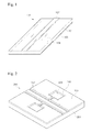
Fig. 3 is an opened-up view of the resonator having a three dimensional DGS in the transmission line according to the first example of the present invention showing the DGS pattern and transmission line with the upper cover removed. -
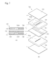
Fig. 4 is a cross-sectional view, cut in the longitudinal direction of the transmission line, of the resonator having a three dimensional DGS in the transmission line according to the first example of the present invention. -
Fig. 5 is an exploded perspective view corresponding to the cross sectional view ofFig. 4 . -
Fig. 6 shows the DGS pattern formed on the lower ground plane member and the configuration of the transmission line on the substrate in the resonator having a three-dimensional DGS in the transmission line according to the first example of the present invention. -
Fig. 7 is a cross-sectional view and an exploded perspective view of the resonator having a three dimensional DGS in the transmission line according to the second example of the present invention. -
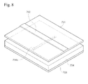
Fig. 8 shows the structure of the slot formed on the center portion of the DGS pattern of the lower ground plane member and the arrangement to the transmission line in the resonator having a three dimensional DGS in the transmission line according to the second example of the present invention. -
Fig. 9 shows frequency characteristics of the resonator with a conventional microstripline DGS. -
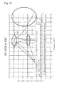
Fig. 10 shows frequency characteristics of the resonator having a three-dimensional DGS in the transmission line according to the present invention. -
- 101,201,301,701...substrate
- 102,202,302,702...transmission line
- 103,203,303,304,703,704...ground plane member
- 104,204,303h,304h,703h,704h...DGS pattern
- 205,310,311...current flow
- 305,705...upper cover
- 306,706...lower cover
- 703s,704s...through slot
- Now the present invention will be described in detail with reference to the drawings attached.
-
Figs. 3-6 show the resonator having a three dimensional DGS in the transmission line according to the first example of the present invention.Fig. 3 is an opened-up view of the resonator having a three dimensional DGS in the transmission line according to the first example of the present invention showing the DGS pattern and transmission line with the upper cover removed.Fig. 4 shows the cross section cut in the longitudinal direction of center line.Fig. 5 is an exploded perspective view corresponding to the cross sectional view ofFig. 4 .Fig. 6 shows detailed structure of the DGS pattern formed on the lower ground plane member and the configuration of the transmission line on the substrate. - Referring to
Figs. 3-6 , theresonator 300 having a three-dimensional DGS in the transmission line according to the first example of the present invention includes asubstrate 301, atransmission line 302, anupper grounding member 303, alower grounding member 304, anupper cover 305 and alower cover 306. - The
substrate 301 is located in the center of the device (the resonator), and installed suspending in the space through supporting member (not illustrated) at both ends of the device. - The
transmission line 302 is installed on the upper surface of thesubstrate 301 for transmitting a signal (communication electromagnetic wave signal, for example). SSS (Suspended Substrate Stripline) can be used for the transmission line. - The upper
ground plane member 303 is installed on the upper surface of thesubstrate 301 with predetermined interval from the surface of the substrate, and aDGS pattern 303h with a predetermined shape is formed on both sides, that is, on each portion of the body of the ground plane member symmetrically with respect to thetransmission line 302 to form a resonator. In forming theDGS pattern 303h, high capacitance can be obtained by forming theDGS pattern 303h controlling the height H and the width W of the gap of the pattern. The upperground plane member 303 is made from conductive material such as Au, Pt or Cu. - The lower
ground plane member 304 is installed on the lower surface of thesubstrate 301 with predetermined interval from the surface of the substrate, and aDGS pattern 304h with a predetermined shape is formed on both sides, that is, on each portion of the body of the ground plane member symmetrically with respect to thetransmission line 302 to form a resonator. The lowerground plane member 303 is made from conductive material such as Au, Pt or Cu. - The
DGS patterns ground plane member 303 and the lowerground plane member 304 respectively are formed to be symmetrical in the shape of a dumbbell with respect to thesubstrate 301 in the vertical plane centering around thesubstrate 301 as shown inFig. 4 as well as symmetrical in the shape of a dumbbell with respect to the transmission line302 in the horizontal plane as shown inFig. 3 . Therefore, the flow of current 310 flows around through both sides of thetransmission line 302 along theDGS pattern Fig. 3 (the flow has the same trace in theDGS pattern 304h of thelower grounding member 304 as that of theDGS pattern 303h of the upper grounding member 303), and the flow of current 311 also flows around through upper and lower parts of thesubstrate 301 along theDGS pattern - The
upper cover 305 is installed closely contacting the upper surface of the upperground plane member 303 to seal the upper opening of theDGS pattern 303h formed on the upperground plane member 303 and to protect the upperground plane member 303 at the same time. Since the upper opening of theDGS pattern 303h formed on the upperground plane member 303 is sealed by theupper cover 305, the radiation of current in the rear direction of the ground plane as in the conventional resonators ofFigs.1 and 2 is prevented thereby preventing transmission loss of signals. Theupper cover 305 is made from the same material as that of the upperground plane member 303 or from different material from that of the upperground plane member 303. - The
lower cover 306 is installed closely contacting the lower surface of the lowerground plane member 304 to seal the lower opening of theDGS pattern 304h formed on the lowerground plane member 304 and to protect the lowerground plane member 304 at the same time. Since the lower opening of theDGS pattern 304h formed on the lowerground plane member 304 is sealed by thelower cover 306, the radiation of current in the rear direction of the ground plane as in the conventional resonators is prevented thereby preventing transmission loss of signals as in the case of theupper cover 305. Thelower cover 306 is made from the same material as that of the lowerground plane member 304 or from different material from that of the lowerground plane member 304. -
Figs. 7 and8 illustrate the resonator having a three dimensional DGS in the transmission line according to the second example of the present invention.Fig. 7 is a cross-sectional view and an exploded perspective view of the resonator andFig. 8 shows the structure of the slot formed on the center portion of the DGS pattern of the lower ground plane member and the arrangement to the transmission line in the substrate. - Referring to
Figs. 7 and8 , theresonator 700 having a three-dimensional DGS in the transmission line according to the second example of the present invention includes asubstrate 701, atransmission line 702, anupper grounding member 703, alower grounding member 704, anupper cover 705 and alower cover 706. - The
substrate 701 is located at the center of the device (the resonator), and installed suspending in the space through supporting member (not illustrated) at both ends of the device. - The
transmission line 702 is installed on the upper surface of thesubstrate 701 for transmitting a signal (communication electromagnetic wave signal, for example). SSS (Suspended Substrate Stripline) can be used for the transmission line. - The upper
ground plane member 703 is installed on the upper surface of thesubstrate 701 with predetermined interval from the surface of the substrate, and aDGS pattern 703h with a rectangular shape is formed perpendicularly crossing thetransmission line 302 to form a resonator. The upperground plane member 703 is made from conductive material such as Au, Pt or Cu. - The lower
ground plane member 704 is installed on the lower surface of thesubstrate 701 with predetermined interval from the surface of the substrate, and aDGS pattern 704h with a rectangular shape is formed perpendicularly crossing thetransmission line 302 to form a resonator. The lowerground plane member 704 is made from conductive material such as Au, Pt or Cu. - The
DGS patterns ground plane member 703 and the lowerground plane member 704 respectively are formed in a way that a rectangular-shaped groove with a predetermined depth from the surface of the surface member is formed on the surface of the upper and lowerground plane members slot slot - The
upper cover 705 is installed closely contacting the upper surface of the upperground plane member 703 to seal the upper opening of theDGS pattern 703h formed on the upperground plane member 703 and to protect the upperground plane member 703 at the same time. Theupper cover 705 is made from the same material as that of the upperground plane member 703 or from different material from that of the upperground plane member 703. - The
lower cover 706 is installed closely contacting the lower surface of the lowerground plane member 704 to seal the lower opening of theDGS pattern 704h formed on the lowerground plane member 704 and to protect the lowerground plane member 704 at the same time. Thelower cover 706 is made from the same material as that of the lowerground plane member 704 or from different material from that of the lowerground plane member 704. - Meanwhile,
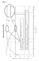
Fig. 9 shows frequency characteristics of the resonator with a conventional microstrip DGS, andFig. 10 shows frequency characteristics of the resonator having a three-dimensional DGS in the transmission line according to the present invention. - As illustrated in
Fig. 9 , in the resonator with a conventional microstrip DGS, signal transmission loss increases by current radiation as frequency increases and shows bad characteristics of reflection wave S11 and transmission wave S21 at resonance frequency. Therefore, it is difficult to obtain high quality factor. Furthermore, electromagnetic wave is emitted in the rear direction of DGS as the frequency increases above resonance frequency thereby eliminating the resonance characteristics. - In the resonator having a three-dimensional DGS in the transmission line according to the present invention, however, there is no loss of signal transmission when the frequency increases as shown in
Fig. 10 . Therefore, good characteristics of reflection wave S11 and transmission wave S21 at resonance frequency can be obtained ensuring high quality factor. Also, it can be seen that the resonance characteristics are maintained even though the frequency increases above resonance frequency. - As described above, the resonator having a three-dimensional DGS in the transmission line according to the present invention form a parallel resonator structure in the right and left sides and in the upper and lower portion of the transmission line based on the SSS transmission line structure, and has the structure wherein the openings of each DGS is sealed by upper and lower cover, ensuring high quality factor by reducing signal transmission loss. Therefore, performance with high credibility can be obtained when the resonator of the present invention is applied to the circuits and modules to which small resonators with super-high frequency range are applied.
- Also, the resonator having a three-dimensional DGS in the transmission line according to the present invention can be applied to the microstrip line structure or rectangular waveguide.
- Although preferable examples of the present invention have been described in detail, they should not be interpreted to limit the present invention, and any obvious modification of the examples by those skilled in the art should be deemed to be included in the scope of the invention as long as the modification is within the technical idea of the present invention. Therefore, the scope of the invention should be interpreted based on the claims of all the technical ideas which are equivalent to that of the present invention should be deemed to be included in the scope of the present invention.
Claims (4)
- A resonator having a three-dimensional DGS in the transmission line, comprising:a substrate installed at the center of the resonator floating in the air through supporting members installed on both ends of the substrate;a transmission line for transmitting signals installed on the upper surface of the substrate;an upper ground plane member installed on the upper surface of the substrate with predetermined interval from the surface of the substrate, wherein a DGS pattern with a predetermined shape is formed on each portion of the body of the ground plane member symmetrically with respect to the transmission line to form a resonator;a lower ground plane member installed on the lower surface of the substrate with predetermined interval from the surface of the substrate, wherein a DGS pattern with a predetermined shape is formed on each portion of the body of the ground plane member symmetrically with respect to the transmission line to form a resonator;an upper cover installed closely contacting the upper surface of the upper ground plane member to seal the upper opening of the DGS pattern formed on the upper ground plane member and to protect the upper ground plane member at the same time; anda lower cover installed closely contacting the lower surface of the lower ground plane member to seal the lower opening of the DGS pattern formed on the lower ground plane member and to protect the lower ground plane member at the same time.
- The resonator according to claim 1, wherein the DGS patterns formed on the upper ground plane member and the lower ground plane member respectively are formed to be symmetrical in the shape of a dumbbell with respect to the substrate in the vertical plane centering around the substrate as well as symmetrical in the shape of a dumbbell with respect to the transmission line in the horizontal plane.
- A resonator having a three-dimensional DGS in the transmission line, comprising:a substrate installed at the center of the resonator floating in the air through supporting members installed on both ends of the substrate;a transmission line for transmitting signals installed on the upper surface of the substrate;an upper ground plane member installed on the upper surface of the substrate with predetermined interval from the surface of the substrate, wherein a DGS pattern with rectangular shape for constructing a resonator is formed perpendicularly to the transmission line;a lower ground plane member installed on the bottom surface of the substrate with predetermined interval from the surface of the substrate, wherein a DGS pattern with rectangular shape for constructing a resonator is formed perpendicularly to the transmission line;an upper cover installed closely contacting the upper surface of the upper ground plane member to seal the upper opening of the DGS pattern formed on the upper ground plane member and to protect the upper ground plane member at the same time; anda lower cover installed closely contacting the lower surface of the lower ground plane member to seal the lower opening of the DGS pattern formed on the lower ground plane member and to protect the lower ground plane member at the same time.
- The resonator according to claim 3, wherein the DGS patterns formed in rectangular shape on the upper ground plane member and the lower ground plane member respectively are formed in a way that a rectangular-shaped groove with a predetermined depth from the surface of the surface member is formed on the surface of the upper and lower ground plane members and a through slot with a predetermined width is formed along the center of the floor of the groove in the longitudinal direction of the groove.
Applications Claiming Priority (1)
| Application Number | Priority Date | Filing Date | Title |
|---|---|---|---|
| KR1020080103045A KR100960044B1 (en) | 2008-10-21 | 2008-10-21 | Resonator with 3D DS on Transmission Line |
Publications (2)
| Publication Number | Publication Date |
|---|---|
| EP2180542A1 true EP2180542A1 (en) | 2010-04-28 |
| EP2180542B1 EP2180542B1 (en) | 2011-04-13 |
Family
ID=40999914
Family Applications (1)
| Application Number | Title | Priority Date | Filing Date |
|---|---|---|---|
| EP09162367A Active EP2180542B1 (en) | 2008-10-21 | 2009-06-10 | Resonator having a three dimensional defected ground structure in transmission line |
Country Status (5)
| Country | Link |
|---|---|
| US (1) | US8018306B2 (en) |
| EP (1) | EP2180542B1 (en) |
| KR (1) | KR100960044B1 (en) |
| AT (1) | ATE505825T1 (en) |
| DE (1) | DE602009001083D1 (en) |
Families Citing this family (7)
| Publication number | Priority date | Publication date | Assignee | Title |
|---|---|---|---|---|
| KR101215885B1 (en) * | 2009-11-13 | 2012-12-27 | 한국전자통신연구원 | Apparatus and method transmission line implementation having left-handed law |
| KR101144565B1 (en) * | 2010-11-10 | 2012-05-11 | 순천향대학교 산학협력단 | Double microstrip transmission line having common defected ground structure and wireless circuit apparatus using the same |
| JP5900174B2 (en) * | 2012-06-08 | 2016-04-06 | 住友電気工業株式会社 | Coherent mixer, method of making coherent mixer |
| KR101984811B1 (en) | 2012-10-23 | 2019-06-03 | 삼성전자주식회사 | Field controllable 3d flexible resonator for wireless power transfer system |
| CN103050754B (en) * | 2012-12-30 | 2014-12-17 | 南京理工大学 | Microstrip line-coplanar stripline broadband transitional structure |
| KR101375581B1 (en) * | 2013-04-26 | 2014-03-18 | 한밭대학교 산학협력단 | Circuit element and method for tunable defected ground structure |
| CN112563704A (en) * | 2019-09-25 | 2021-03-26 | 天津大学 | Self-packaged wide-stop-band-pass filter based on medium integrated suspension line |
Citations (5)
| Publication number | Priority date | Publication date | Assignee | Title |
|---|---|---|---|---|
| US4426649A (en) * | 1980-07-23 | 1984-01-17 | L'etat Francais, Represente Par Le Secretaire D'etat Aux Postes Et Des A La Telediffusion (Centre National D'etudes Des Telecommunications) | Folded back doublet antenna for very high frequencies and networks of such doublets |
| EP0245890A2 (en) * | 1986-05-14 | 1987-11-19 | Siemens Telecomunicazioni S.P.A. | Microstrip transmission line for coupling to a dielectric resonator |
| GB2212665A (en) * | 1987-11-23 | 1989-07-26 | Gen Electric Co Plc | Slot antenna |
| US6023210A (en) * | 1998-03-03 | 2000-02-08 | California Institute Of Technology | Interlayer stripline transition |
| EP1170817A1 (en) * | 2000-07-04 | 2002-01-09 | Dal Ahn | Transmission line resonator with dielectric substrate having an etched structure on the ground plane |
Family Cites Families (8)
| Publication number | Priority date | Publication date | Assignee | Title |
|---|---|---|---|---|
| US3863181A (en) * | 1973-12-03 | 1975-01-28 | Bell Telephone Labor Inc | Mode suppressor for strip transmission lines |
| JP3929197B2 (en) * | 1999-03-17 | 2007-06-13 | 松下電器産業株式会社 | High frequency circuit element |
| JP3062886B1 (en) | 1999-03-23 | 2000-07-12 | 株式会社移動体通信先端技術研究所 | Three-dimensional superconducting resonator and three-dimensional superconducting filter |
| JP3650957B2 (en) * | 1999-07-13 | 2005-05-25 | 株式会社村田製作所 | Transmission line, filter, duplexer and communication device |
| KR100521895B1 (en) * | 2003-02-07 | 2005-10-14 | 박익모 | Lowpass Filter Using CPW Structure with Inductive Etched Hole |
| KR100538889B1 (en) * | 2003-02-10 | 2005-12-26 | 임종식 | A New Type of Low Pass Filters Using Defected Ground Structure and Capacitively Compensated Transmission Line |
| TWI254483B (en) * | 2005-01-19 | 2006-05-01 | Yung-Ling Lai | Defected ground structure for coplanar waveguides |
| EP2160791A1 (en) * | 2007-06-28 | 2010-03-10 | BAE Systems PLC | Microwave circuit assembly |
-
2008
- 2008-10-21 KR KR1020080103045A patent/KR100960044B1/en not_active Expired - Fee Related
-
2009
- 2009-06-08 US US12/480,081 patent/US8018306B2/en active Active
- 2009-06-10 AT AT09162367T patent/ATE505825T1/en not_active IP Right Cessation
- 2009-06-10 DE DE602009001083T patent/DE602009001083D1/en active Active
- 2009-06-10 EP EP09162367A patent/EP2180542B1/en active Active
Patent Citations (5)
| Publication number | Priority date | Publication date | Assignee | Title |
|---|---|---|---|---|
| US4426649A (en) * | 1980-07-23 | 1984-01-17 | L'etat Francais, Represente Par Le Secretaire D'etat Aux Postes Et Des A La Telediffusion (Centre National D'etudes Des Telecommunications) | Folded back doublet antenna for very high frequencies and networks of such doublets |
| EP0245890A2 (en) * | 1986-05-14 | 1987-11-19 | Siemens Telecomunicazioni S.P.A. | Microstrip transmission line for coupling to a dielectric resonator |
| GB2212665A (en) * | 1987-11-23 | 1989-07-26 | Gen Electric Co Plc | Slot antenna |
| US6023210A (en) * | 1998-03-03 | 2000-02-08 | California Institute Of Technology | Interlayer stripline transition |
| EP1170817A1 (en) * | 2000-07-04 | 2002-01-09 | Dal Ahn | Transmission line resonator with dielectric substrate having an etched structure on the ground plane |
Also Published As
| Publication number | Publication date |
|---|---|
| DE602009001083D1 (en) | 2011-05-26 |
| ATE505825T1 (en) | 2011-04-15 |
| US20100097163A1 (en) | 2010-04-22 |
| KR20100043832A (en) | 2010-04-29 |
| KR100960044B1 (en) | 2010-05-31 |
| US8018306B2 (en) | 2011-09-13 |
| EP2180542B1 (en) | 2011-04-13 |
Similar Documents
| Publication | Publication Date | Title |
|---|---|---|
| US8018306B2 (en) | Resonator having a three dimensional defected ground structure in transmission line | |
| US8040200B2 (en) | Parallel differential transmission lines having an opposing grounding conductor separated into two parts by a slot therein | |
| KR101158559B1 (en) | Contact-free element of transition between a waveguide and a microstrip line | |
| JP5566169B2 (en) | Antenna device | |
| CN110350282B (en) | Directional coupler based on double-ridge integrated substrate gap waveguide | |
| KR20110075795A (en) | Transition Structure and Application Module between Microstrip Line and Suspended Strip Line | |
| TWI923981B (en) | Antenna assembly and communication terminal | |
| US20150222003A1 (en) | Microwave circuit | |
| CN110676550B (en) | Microstrip Vertical Transition Structure and Microwave Devices | |
| US20080136550A1 (en) | Line transition device, high-frequency module, and communication apparatus | |
| JP3958351B2 (en) | Transmission line equipment | |
| CN209592277U (en) | A Novel ISGW Bandpass Filter with Dual Transmission Zeros and Wide Stopband | |
| JP5126625B2 (en) | Compact filtering structure | |
| FI126467B (en) | RF filter | |
| US12206149B2 (en) | Dielectric waveguide resonator and filter including at least one internal conductor physically isolated from first and second surface conductors and overlapping therewith | |
| US20150008991A1 (en) | Planar circuit to waveguide transition | |
| US20190190107A1 (en) | Planar orthomode transducer | |
| US7595707B2 (en) | Microstripline type directional coupler and communication device using the same | |
| CN117060053A (en) | A low-profile filtered dielectric resonator antenna based on metal bridge loading | |
| CN210272629U (en) | A Novel Directional Coupler Based on Double Ridge Integrated Substrate Gap Waveguide | |
| CN116632473B (en) | Filters and circuit components | |
| CN117691965B (en) | Filter containing half-mode substrate coaxial resonator | |
| US12218396B2 (en) | Multi-layered band-pass filter device | |
| US10270147B2 (en) | Dielectric waveguide, mounting structure for a dielectric waveguide, dielectric waveguide filter and massive MIMO system | |
| JP2005244932A (en) | Variable frequency type high frequency filter |
Legal Events
| Date | Code | Title | Description |
|---|---|---|---|
| PUAI | Public reference made under article 153(3) epc to a published international application that has entered the european phase |
Free format text: ORIGINAL CODE: 0009012 |
|
| 17P | Request for examination filed |
Effective date: 20090701 |
|
| AK | Designated contracting states |
Kind code of ref document: A1 Designated state(s): AT BE BG CH CY CZ DE DK EE ES FI FR GB GR HR HU IE IS IT LI LT LU LV MC MK MT NL NO PL PT RO SE SI SK TR |
|
| AX | Request for extension of the european patent |
Extension state: AL BA RS |
|
| GRAP | Despatch of communication of intention to grant a patent |
Free format text: ORIGINAL CODE: EPIDOSNIGR1 |
|
| GRAS | Grant fee paid |
Free format text: ORIGINAL CODE: EPIDOSNIGR3 |
|
| GRAA | (expected) grant |
Free format text: ORIGINAL CODE: 0009210 |
|
| AK | Designated contracting states |
Kind code of ref document: B1 Designated state(s): AT BE BG CH CY CZ DE DK EE ES FI FR GB GR HR HU IE IS IT LI LT LU LV MC MK MT NL NO PL PT RO SE SI SK TR |
|
| REG | Reference to a national code |
Ref country code: GB Ref legal event code: FG4D |
|
| REG | Reference to a national code |
Ref country code: CH Ref legal event code: EP |
|
| REG | Reference to a national code |
Ref country code: IE Ref legal event code: FG4D |
|
| REF | Corresponds to: |
Ref document number: 602009001083 Country of ref document: DE Date of ref document: 20110526 Kind code of ref document: P |
|
| REG | Reference to a national code |
Ref country code: DE Ref legal event code: R096 Ref document number: 602009001083 Country of ref document: DE Effective date: 20110526 |
|
| REG | Reference to a national code |
Ref country code: NL Ref legal event code: VDEP Effective date: 20110413 |
|
| LTIE | Lt: invalidation of european patent or patent extension |
Effective date: 20110413 |
|
| PG25 | Lapsed in a contracting state [announced via postgrant information from national office to epo] |
Ref country code: SE Free format text: LAPSE BECAUSE OF FAILURE TO SUBMIT A TRANSLATION OF THE DESCRIPTION OR TO PAY THE FEE WITHIN THE PRESCRIBED TIME-LIMIT Effective date: 20110413 Ref country code: NO Free format text: LAPSE BECAUSE OF FAILURE TO SUBMIT A TRANSLATION OF THE DESCRIPTION OR TO PAY THE FEE WITHIN THE PRESCRIBED TIME-LIMIT Effective date: 20110713 Ref country code: HR Free format text: LAPSE BECAUSE OF FAILURE TO SUBMIT A TRANSLATION OF THE DESCRIPTION OR TO PAY THE FEE WITHIN THE PRESCRIBED TIME-LIMIT Effective date: 20110413 Ref country code: PT Free format text: LAPSE BECAUSE OF FAILURE TO SUBMIT A TRANSLATION OF THE DESCRIPTION OR TO PAY THE FEE WITHIN THE PRESCRIBED TIME-LIMIT Effective date: 20110816 Ref country code: LT Free format text: LAPSE BECAUSE OF FAILURE TO SUBMIT A TRANSLATION OF THE DESCRIPTION OR TO PAY THE FEE WITHIN THE PRESCRIBED TIME-LIMIT Effective date: 20110413 |
|
| PG25 | Lapsed in a contracting state [announced via postgrant information from national office to epo] |
Ref country code: AT Free format text: LAPSE BECAUSE OF FAILURE TO SUBMIT A TRANSLATION OF THE DESCRIPTION OR TO PAY THE FEE WITHIN THE PRESCRIBED TIME-LIMIT Effective date: 20110413 Ref country code: CY Free format text: LAPSE BECAUSE OF FAILURE TO SUBMIT A TRANSLATION OF THE DESCRIPTION OR TO PAY THE FEE WITHIN THE PRESCRIBED TIME-LIMIT Effective date: 20110413 Ref country code: BE Free format text: LAPSE BECAUSE OF FAILURE TO SUBMIT A TRANSLATION OF THE DESCRIPTION OR TO PAY THE FEE WITHIN THE PRESCRIBED TIME-LIMIT Effective date: 20110413 Ref country code: ES Free format text: LAPSE BECAUSE OF FAILURE TO SUBMIT A TRANSLATION OF THE DESCRIPTION OR TO PAY THE FEE WITHIN THE PRESCRIBED TIME-LIMIT Effective date: 20110724 Ref country code: LV Free format text: LAPSE BECAUSE OF FAILURE TO SUBMIT A TRANSLATION OF THE DESCRIPTION OR TO PAY THE FEE WITHIN THE PRESCRIBED TIME-LIMIT Effective date: 20110413 Ref country code: GR Free format text: LAPSE BECAUSE OF FAILURE TO SUBMIT A TRANSLATION OF THE DESCRIPTION OR TO PAY THE FEE WITHIN THE PRESCRIBED TIME-LIMIT Effective date: 20110714 Ref country code: SI Free format text: LAPSE BECAUSE OF FAILURE TO SUBMIT A TRANSLATION OF THE DESCRIPTION OR TO PAY THE FEE WITHIN THE PRESCRIBED TIME-LIMIT Effective date: 20110413 Ref country code: IS Free format text: LAPSE BECAUSE OF FAILURE TO SUBMIT A TRANSLATION OF THE DESCRIPTION OR TO PAY THE FEE WITHIN THE PRESCRIBED TIME-LIMIT Effective date: 20110813 Ref country code: FI Free format text: LAPSE BECAUSE OF FAILURE TO SUBMIT A TRANSLATION OF THE DESCRIPTION OR TO PAY THE FEE WITHIN THE PRESCRIBED TIME-LIMIT Effective date: 20110413 |
|
| PG25 | Lapsed in a contracting state [announced via postgrant information from national office to epo] |
Ref country code: NL Free format text: LAPSE BECAUSE OF FAILURE TO SUBMIT A TRANSLATION OF THE DESCRIPTION OR TO PAY THE FEE WITHIN THE PRESCRIBED TIME-LIMIT Effective date: 20110413 Ref country code: MT Free format text: LAPSE BECAUSE OF FAILURE TO SUBMIT A TRANSLATION OF THE DESCRIPTION OR TO PAY THE FEE WITHIN THE PRESCRIBED TIME-LIMIT Effective date: 20110413 |
|
| PG25 | Lapsed in a contracting state [announced via postgrant information from national office to epo] |
Ref country code: EE Free format text: LAPSE BECAUSE OF FAILURE TO SUBMIT A TRANSLATION OF THE DESCRIPTION OR TO PAY THE FEE WITHIN THE PRESCRIBED TIME-LIMIT Effective date: 20110413 Ref country code: CZ Free format text: LAPSE BECAUSE OF FAILURE TO SUBMIT A TRANSLATION OF THE DESCRIPTION OR TO PAY THE FEE WITHIN THE PRESCRIBED TIME-LIMIT Effective date: 20110413 |
|
| PLBE | No opposition filed within time limit |
Free format text: ORIGINAL CODE: 0009261 |
|
| STAA | Information on the status of an ep patent application or granted ep patent |
Free format text: STATUS: NO OPPOSITION FILED WITHIN TIME LIMIT |
|
| PG25 | Lapsed in a contracting state [announced via postgrant information from national office to epo] |
Ref country code: SK Free format text: LAPSE BECAUSE OF FAILURE TO SUBMIT A TRANSLATION OF THE DESCRIPTION OR TO PAY THE FEE WITHIN THE PRESCRIBED TIME-LIMIT Effective date: 20110413 Ref country code: PL Free format text: LAPSE BECAUSE OF FAILURE TO SUBMIT A TRANSLATION OF THE DESCRIPTION OR TO PAY THE FEE WITHIN THE PRESCRIBED TIME-LIMIT Effective date: 20110413 |
|
| 26N | No opposition filed |
Effective date: 20120116 |
|
| REG | Reference to a national code |
Ref country code: FR Ref legal event code: ST Effective date: 20120229 |
|
| REG | Reference to a national code |
Ref country code: IE Ref legal event code: MM4A |
|
| REG | Reference to a national code |
Ref country code: DE Ref legal event code: R119 Ref document number: 602009001083 Country of ref document: DE Effective date: 20120103 |
|
| PG25 | Lapsed in a contracting state [announced via postgrant information from national office to epo] |
Ref country code: DE Free format text: LAPSE BECAUSE OF NON-PAYMENT OF DUE FEES Effective date: 20120103 Ref country code: IE Free format text: LAPSE BECAUSE OF NON-PAYMENT OF DUE FEES Effective date: 20110610 Ref country code: FR Free format text: LAPSE BECAUSE OF NON-PAYMENT OF DUE FEES Effective date: 20110630 |
|
| PG25 | Lapsed in a contracting state [announced via postgrant information from national office to epo] |
Ref country code: IT Free format text: LAPSE BECAUSE OF FAILURE TO SUBMIT A TRANSLATION OF THE DESCRIPTION OR TO PAY THE FEE WITHIN THE PRESCRIBED TIME-LIMIT Effective date: 20110413 |
|
| PG25 | Lapsed in a contracting state [announced via postgrant information from national office to epo] |
Ref country code: MK Free format text: LAPSE BECAUSE OF FAILURE TO SUBMIT A TRANSLATION OF THE DESCRIPTION OR TO PAY THE FEE WITHIN THE PRESCRIBED TIME-LIMIT Effective date: 20110413 |
|
| PG25 | Lapsed in a contracting state [announced via postgrant information from national office to epo] |
Ref country code: MC Free format text: LAPSE BECAUSE OF NON-PAYMENT OF DUE FEES Effective date: 20110630 |
|
| PG25 | Lapsed in a contracting state [announced via postgrant information from national office to epo] |
Ref country code: LU Free format text: LAPSE BECAUSE OF NON-PAYMENT OF DUE FEES Effective date: 20110610 |
|
| PG25 | Lapsed in a contracting state [announced via postgrant information from national office to epo] |
Ref country code: BG Free format text: LAPSE BECAUSE OF FAILURE TO SUBMIT A TRANSLATION OF THE DESCRIPTION OR TO PAY THE FEE WITHIN THE PRESCRIBED TIME-LIMIT Effective date: 20110713 |
|
| PG25 | Lapsed in a contracting state [announced via postgrant information from national office to epo] |
Ref country code: TR Free format text: LAPSE BECAUSE OF FAILURE TO SUBMIT A TRANSLATION OF THE DESCRIPTION OR TO PAY THE FEE WITHIN THE PRESCRIBED TIME-LIMIT Effective date: 20110413 |
|
| PG25 | Lapsed in a contracting state [announced via postgrant information from national office to epo] |
Ref country code: HU Free format text: LAPSE BECAUSE OF FAILURE TO SUBMIT A TRANSLATION OF THE DESCRIPTION OR TO PAY THE FEE WITHIN THE PRESCRIBED TIME-LIMIT Effective date: 20110413 |
|
| REG | Reference to a national code |
Ref country code: CH Ref legal event code: PL |
|
| PG25 | Lapsed in a contracting state [announced via postgrant information from national office to epo] |
Ref country code: LI Free format text: LAPSE BECAUSE OF NON-PAYMENT OF DUE FEES Effective date: 20130630 Ref country code: CH Free format text: LAPSE BECAUSE OF NON-PAYMENT OF DUE FEES Effective date: 20130630 |
|
| PGFP | Annual fee paid to national office [announced via postgrant information from national office to epo] |
Ref country code: GB Payment date: 20240620 Year of fee payment: 16 |
|
| GBPC | Gb: european patent ceased through non-payment of renewal fee |
Effective date: 20250610 |
|
| PG25 | Lapsed in a contracting state [announced via postgrant information from national office to epo] |
Ref country code: GB Free format text: LAPSE BECAUSE OF NON-PAYMENT OF DUE FEES Effective date: 20250610 |