EP2180312A2 - Plasma etch process sensor - Google Patents
Plasma etch process sensor Download PDFInfo
- Publication number
- EP2180312A2 EP2180312A2 EP09252229A EP09252229A EP2180312A2 EP 2180312 A2 EP2180312 A2 EP 2180312A2 EP 09252229 A EP09252229 A EP 09252229A EP 09252229 A EP09252229 A EP 09252229A EP 2180312 A2 EP2180312 A2 EP 2180312A2
- Authority
- EP
- European Patent Office
- Prior art keywords
- silane
- silane deposition
- sensor
- deposition
- plasma
- Prior art date
- Legal status (The legal status is an assumption and is not a legal conclusion. Google has not performed a legal analysis and makes no representation as to the accuracy of the status listed.)
- Granted
Links
Images

Classifications
-
- G—PHYSICS
- G01—MEASURING; TESTING
- G01N—INVESTIGATING OR ANALYSING MATERIALS BY DETERMINING THEIR CHEMICAL OR PHYSICAL PROPERTIES
- G01N21/00—Investigating or analysing materials by the use of optical means, i.e. using sub-millimetre waves, infrared, visible or ultraviolet light
- G01N21/62—Systems in which the material investigated is excited whereby it emits light or causes a change in wavelength of the incident light
- G01N21/71—Systems in which the material investigated is excited whereby it emits light or causes a change in wavelength of the incident light thermally excited
- G01N21/73—Systems in which the material investigated is excited whereby it emits light or causes a change in wavelength of the incident light thermally excited using plasma burners or torches
Definitions
- the present invention relates to a method and device for monitoring silane deposition. More particularly, the present invention relates to a method and device for determining whether a component in a plasma processing apparatus has been silanized.
- Silanes are a class of chemical compounds containing silicon and hydrogen. Silane has the generic chemical formula of SiH 4 and is the silicon analog of methane. A silane is often applied to bonding surfaces of aircraft components, such as fan inlet shroud fairings, prior to bonding the component to a frame or other component. Different types of silanes are used to improve the bonding properties of components, whether they are for aircraft or other commercial uses. Silanes generally improve the strength and integrity of the bond between components.
- One embodiment of the present invention relates to a method of monitoring silane deposition in a plasma processing apparatus.
- the method includes placing a silane deposition sensor within a processing vessel in proximity with a plasma field receptor.
- the method further includes introducing a silane into the processing vessel, applying electromagnetic radiation within the processing vessel, and optically assessing the silane deposition sensor for silane.
- the system includes a processing vessel having an inlet for introducing silane and a power unit for applying electromagnetic radiation, a silane deposition sensor and a plasma field receptor located in proximity with the silane deposition sensor.
- An additional embodiment of the system includes a silane deposition housing, a plasma field receptor, a light source and a photosensor.
- the silane deposition housing includes an interior region, a window and an outer surface. The window allows passage of light from the light source located within the interior region. The photosensor senses light transmitted through the window and transmits a signal.
- Recent advances in plasma technology have allowed engineers to apply a thin layer of silane to components using plasmas.
- silane layers were typically brushed onto components prior to bonding.
- Plasma silanization of a component is performed inside a plasma processing apparatus upon introduction of a silane into a processing vessel of the plasma processing apparatus and the application of electromagnetic radiation.
- the thin layer of silane offers the same functionality as the brushed on silane while providing additional advantages during application.
- silanization is that because only a thin layer of silane is applied to a component, a silanized component is visually indistinguishable from a non-silanized one. Expensive chromatographic or spectrophotometric techniques are required to verify whether a component contains a silane layer. At times, plasma processing operators may forget or not know whether a component within the processing vessel has been silanized or not. Thus, a way to determine whether silanization has taken place without using expensive techniques is desired.
- a thin layer of silane can be applied to a component using plasma technology.
- One method of applying a thin layer of silane to a component includes a multi-step process using plasmas. First, the component is placed in a plasma processing apparatus. Second, the component is "cleaned” with a plasma inside the apparatus. “Cleaning” refers to removing contaminants and weak boundary layers from the surface of the component. Suitable gases for cleaning include argon, oxygen, tetrafluoromethane, hydrogen and combinations thereof. Third, the component surfaces are "hydroxylated” with a plasma. “Hydroxylation” refers to the addition of hydroxyl (-OH) groups onto the surface of the component.
- Suitable hydroxylating agents include argon, water vapor, hydrogen peroxide, methanol and combinations thereof.
- the component surfaces are "silanized” with a plasma. "Silanization” refers to the addition of a silane layer through self-assembly to the surface of the component.
- the type of silane chosen for bonding preparation depends on the adhesive used for bonding.
- Suitable vinyl silanes include vinyltrimethylsilane, vinyltrimethylethoxysilane, vinyldimethylethoxysilane, vinyltrimethoxypropylsilane and 3-aminopropylethoxysilane. Because the layer of silane applied to a component is thin (on the order of about 100 nm) it is difficult to determine whether a component has been silanized or not.
- the present invention was developed while observing silane deposition behavior using plasma.
- Silane deposition using plasma is carried out in a processing vessel.
- processing vessels contain one or more metal shelves.
- Components that are treated within the processing vessel are generally placed on a metal shelf during operation. Applicants observed that when a component was located on one of the metal shelves within the processing vessel, excess silane was deposited on the component in the vicinity of the metal shelf. The excess silane was evidenced by a white, opaque band.
- silane deposition sensor 32 is merely placed on metal shelf 18. In alternate embodiments, silane deposition sensor 32 is fastened or attached to metal shelf 18. Screws or clamps and other fastening or attachment means are suitable for fastening or attaching silane deposition sensor 32 to metal shelf 18. Metal shelf 18 acts as a plasma field receptor, as discussed below.
- Components C to be silanized are placed in processing vessel 12.
- Plasma silanization occurs inside processing vessel 12.
- One or more silanes, such as those described above, are introduced into processing vessel 12 by inlet 16. Once introduction of silane has commenced, a predetermined amount of electromagnetic radiation R is applied inside processing vessel 12. The combination of the silane and electromagnetic radiation R results in a silane plasma P and silane is deposited on components C placed within processing vessel 12. Silane is also deposited on silane deposition sensor 32 during plasma silanization.
- silane deposition sensor 32 Due to the proximity between silane deposition sensor 32 and metal shelf 18, an increased level of silanization occurs on silane deposition sensor 32.
- Metal shelf 18 acts as a plasma field receptor and increases the rate of silane deposition on silane deposition sensor 32.
- the presence of a plasma field receptor in proximity to silane deposition sensor 32 affects the electromagnetic field in the area of silane deposition sensor 32 and causes increased chemical reactions between a silane and silane deposition sensor 32. The increased chemical reactions result in an increased rate of silane deposition during plasma silanization.
- FIG. 3 illustrates the silane deposition monitoring system 30 of FIG. 2 after plasma silanization has taken place.
- Silane deposition band 34 is present on silane deposition sensor 32 following plasma silanization.
- Silane deposition band 34 indicates an excess of silane.
- the presence of a plasma field receptor (metal shelf 18) in proximity to silane deposition sensor 32 causes an increase in the rate of silane deposition.
- a thicker layer of silane is deposited on silane deposition sensor 32 in the area of silane deposition band 34: This thicker layer of silane is visually perceptible on silane deposition sensor 32 as a white, opaque band.
- exemplary embodiments of silane deposition sensor 32 are of a color that offers sufficient contrast from white as described above.
- a plasma processing operator can determine if the plasma silanization step has been performed for a component or set of components by inspecting silane deposition sensor 32.
- the presence of a white, opaque band on silane deposition sensor 32 confirms that plasma silanization has taken place within the processing vessel 12.
- An absence of a white, opaque band on silane deposition sensor 32 tells the operator that plasma silanization has yet to take place.
- areas of silane deposition sensor 32 that do not display a white, opaque band of silane contain only a thin layer of silane. This thin layer of silane is the same as what is desired for preparing a component for bonding.
- silane deposition sensor 32 is removed from silane deposition monitoring system 30 and placed along with the silanized component(s) C to verify that silanization has been performed farther downstream in the manufacturing or bonding process. In other instances, silane deposition sensor 32 remains with silane deposition monitoring system 30 or is discarded.
- silane deposition sensor 32 is reusable. After the plasma silanization is complete and silanization is verified, silane deposition sensor 32 is prepared for reuse. Silane deposition band 34 is removed from silane deposition sensor 32. Suitable methods of silane deposition band 34 removal include wiping silane deposition sensor 32 with a cloth, rinsing silane deposition sensor 32 with a solvent capable of dissolving silane, or a combination of the two. In an exemplary embodiment of silane deposition monitoring system 30 where silane deposition sensor 32 is reused, silane deposition sensor 32 has a smooth surface. A smooth surface ensures that silane deposition band 34 can be removed from silane deposition sensor 32.
- silane deposition monitoring system 30 includes a disposable silane deposition sensor 32, which is discarded after use.
- FIG. 4 illustrates one embodiment of silane deposition monitoring system 40.
- Silane deposition monitoring system 40 includes silane deposition sensor 32, metal shelf 18, plasma field isolator 46 and plasma field receptor 48.
- the composition of silane deposition sensor 32 is the same as described above.
- Plasma field isolator 46 is located between silane deposition sensor 32 and metal shelf 18.
- Plasma field isolator 46 is a non-metal material and spaces silane deposition sensor 32 from metal shelf 18.
- plasma field isolator 46 is polyethylene. Plasma field isolator 46 prevents metal shelf 18 from acting as a plasma field receptor to silane deposition sensor 32 as described above.
- Plasma field receptor 48 is typically a metal object.
- Plasma field receptor 48 is typically stainless steel, but other metals that act as plasma field receptors are also suitable.
- plasma field receptor 48 is a stainless steel washer.
- Plasma field receptor 48 increases the rate of silane deposition on silane deposition sensor 32.
- the presence of a plasma field receptor in proximity to silane deposition sensor 32 affects the electromagnetic filed in the area of silane deposition sensor 32 and causes increased chemical reactions between silanes and silane deposition sensor 32. The increased chemical reactions result in an increased rate of silane deposition during plasma silanization.
- FIG. 4 illustrates silane deposition monitoring system 40 following plasma silanization.
- Silane deposition band 34 is present on silane deposition sensor 32.
- Silane deposition monitoring systems 30, 40 provide for a method of monitoring silane deposition in processing vessel 12.
- FIG. 5 illustrates a flow diagram showing the steps involved in one embodiment of a method of monitoring silane deposition 50. The method allows a determination of whether plasma silanization has taken place.
- a silane deposition sensor 32 is placed within processing vessel 12.
- Silane deposition sensor 32 is arranged within processing vessel 12 to be located in proximity with a plasma field receptor.
- silane deposition sensor 32 is in proximity to metal shelf 18.
- silane deposition monitoring system 40 shows silane deposition sensor 32 is in proximity to plasma field receptor 48.
- a silane or mixture of silanes is introduced into processing vessel 12.
- step 56 electromagnetic radiation is applied within processing vessel 12 to initiate plasma silanization. Additional silane may be introduced into processing vessel 12 during step 56. In some embodiments, step 56 occurs following introduction of oxygen, argon or a mixture of oxygen and argon and application of electromagnetic radiation. Steps 54 and 56 are typically performed for a predetermined length of time depending on the silane and the amount of electromagnetic radiation applied.
- step 58 a plasma processing operator visually inspects silane deposition sensor 32 to assess whether plasma silanization has taken place. The presence of silane deposition band 34 on silane deposition sensor 32 confirms that plasma silanization has occurred. The absence of silane deposition band 34 on silane deposition sensor 32 indicates that plasma silanization has not yet been performed.
- silane deposition monitoring system 60 includes silane deposition housing 62, metal shelf 18, plasma field isolator 46, plasma field receptor 48, light source 64 and photosensor 66.
- the composition and function of metal shelf 18, plasma field isolator 46, and plasma field receptor 48 are the same as described above.
- Silane deposition housing 62 includes interior region 68, outer surface 70 and window 72.
- Interior region 68 allows for the placement of light source 64 within silane deposition housing 62.
- Outer surface 70 functions similarly to silane deposition sensor 32.
- Window 72 is generally positioned on silane deposition housing 62 in a location where silane deposition band 34 is deposited during plasma silanization. Window 72 is transparent.
- silane deposition housing 62 is an optically clear plastic, such as polycarbonate, allyl diglycol carbonate, polymethyl methacrylate, and styrene copolymers. Areas of outer surface 70 of silane deposition housing 62 that do not receive excess deposition of silane during plasma silanization are covered. Suitable materials for covering outer surface 70 include paint, other opaque coatings or opaque fabrics or adhesive materials. Window 72 is formed in an area in which outer surface 70 is not covered. In other embodiments, silane deposition housing 62 is formed from glass, such as soda-lime, borosilicate or quartz, or ceramics, such as mica or aluminum oxynitride. The area of silane deposition housing 62 where excess silane is deposited during plasma silanization contains a transparent material, such as an optically clear plastic, to form window 72.
- a transparent material such as an optically clear plastic
- Light source 64 is positioned in interior region 68 of silane deposition housing 62.
- light source 64 is an electric bulb.
- light source 64 is a light emitting diode.
- light source 64 is an optical fiber.
- Light source 64 is positioned and configured to emit light through window 72 of silane deposition housing 62.
- Photosensor 66 is generally located near outer surface 70 of silane deposition housing 62. Photosensor 66 is configured to sense light emitted through window 72 by light source 64. Photosensor 66 is also configured to transmit a signal based on the amount of light sensed. Suitable types of photosensors 66 include photoresistors, photovoltaic cells and photomultipliers. In the embodiment illustrated in FIG. 6 , photosensor 66 is shown connected to plasma field receptor 48 and located near window 72. In other embodiments, photosensor 66 is not connected to plasma field receptor 48, but a generally uninterrupted path between window 72 and photosensor 66 exists.
- silane deposition monitoring system 60 includes a cover (not shown) to prevent ambient light within plasma processing apparatus 10 from being sensed by photosensor 66. When present, the cover prevents ambient light from entering silane deposition monitoring system 60, but allows chamber gases and plasmas to enter silane deposition monitoring system 60.
- Silane deposition monitoring system 60 provides for a quantitative method of monitoring silane deposition. Steps 52, 54 and 56 of method of monitoring silane deposition 50 ( FIG. 5 ) are followed to initiate plasma silanization.
- Light source 64 is activated so that it emits light prior to or at the beginning of step 56. Prior to plasma silanization, window 72 is transparent. Light from light source 64 travels through window 72 and is sensed by photosensor 66. Photosensor 66 transmits a baseline sense signal indicating that it senses a baseline amount of light.
- silane is deposited on outer surface 70 of silane deposition housing 62. As silane is deposited, window 72 becomes increasingly obscured by silane deposition. The opacity of window 72 increases as plasma silanization continues.
- photosensor 66 transmits a sense signal indicating the amount of light sensed. As the opacity of window 72 increases, light scatters and photosensor 66 senses less light from light source 64. The sense signal transmitted by photosensor 66 then changes from the baseline signal. The change in signal can be used to quantitatively determine an endpoint for plasma silanization. Once a predetermined signal threshold is reached, plasma silanization can be discontinued. Depending on the desired amount of silanization, plasma silanization can be discontinued once window 72 has a desired level of opacity.
- Silane deposition monitoring system 60 allows for real-time monitoring of plasma silanization.
- plasma silanization is automated based on the signals transmitted by photosensor 66.
- Silane deposition monitoring system 60 generates an electronic record to document that plasma silanization has been performed and to what degree.
- a plasma processing operator determines an endpoint for plasma silanization based upon the signals transmitted by photosensor 66.
- the present invention relates to a method of monitoring silane deposition and a monitoring system.
- the method and system allow a plasma processing operator to assess whether components have been silanized. The assessment is made visually by an operator or is automated using a photosensor. Such a method and system allow an operator to verify silanization without the need for expensive chromatographic or spectrophotometric equipment.
- the present invention allows operators to know the condition of components after shift changes and provides an electronic record of silanization or a visual reminder to operators that have stepped away from plasma processing apparatus 10 to perform other tasks.
Landscapes
- Health & Medical Sciences (AREA)
- Physics & Mathematics (AREA)
- Chemical & Material Sciences (AREA)
- Plasma & Fusion (AREA)
- Nuclear Medicine, Radiotherapy & Molecular Imaging (AREA)
- Life Sciences & Earth Sciences (AREA)
- Engineering & Computer Science (AREA)
- Analytical Chemistry (AREA)
- Biochemistry (AREA)
- General Health & Medical Sciences (AREA)
- General Physics & Mathematics (AREA)
- Immunology (AREA)
- Pathology (AREA)
- Chemical Vapour Deposition (AREA)
Abstract
Description
- The present invention relates to a method and device for monitoring silane deposition. More particularly, the present invention relates to a method and device for determining whether a component in a plasma processing apparatus has been silanized.
- Silanes are a class of chemical compounds containing silicon and hydrogen. Silane has the generic chemical formula of SiH4 and is the silicon analog of methane. A silane is often applied to bonding surfaces of aircraft components, such as fan inlet shroud fairings, prior to bonding the component to a frame or other component. Different types of silanes are used to improve the bonding properties of components, whether they are for aircraft or other commercial uses. Silanes generally improve the strength and integrity of the bond between components.
- One embodiment of the present invention relates to a method of monitoring silane deposition in a plasma processing apparatus. The method includes placing a silane deposition sensor within a processing vessel in proximity with a plasma field receptor. The method further includes introducing a silane into the processing vessel, applying electromagnetic radiation within the processing vessel, and optically assessing the silane deposition sensor for silane.
- Additional embodiments of the present invention relate to a silane deposition monitoring system. In one embodiment, the system includes a processing vessel having an inlet for introducing silane and a power unit for applying electromagnetic radiation, a silane deposition sensor and a plasma field receptor located in proximity with the silane deposition sensor. An additional embodiment of the system includes a silane deposition housing, a plasma field receptor, a light source and a photosensor. The silane deposition housing includes an interior region, a window and an outer surface. The window allows passage of light from the light source located within the interior region. The photosensor senses light transmitted through the window and transmits a signal.
-
-
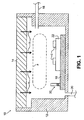
FIG. 1 is a view showing the arrangement of a plasma processing apparatus. -
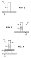
FIG. 2 is a side view of a silane deposition monitoring system. -
FIG. 3 is a side view of a silane deposition monitoring system having a silane deposition band. -
FIG. 4 is a side view of an alternate embodiment of a silane deposition monitoring system having a silane deposition band. -
FIG. 5 is a flow diagram showing one embodiment of a method for monitoring silane deposition. -
FIG. 6 is a side view of a silane deposition monitoring system with a photosensor. - Recent advances in plasma technology have allowed engineers to apply a thin layer of silane to components using plasmas. Until now, silane layers were typically brushed onto components prior to bonding. Plasma silanization of a component is performed inside a plasma processing apparatus upon introduction of a silane into a processing vessel of the plasma processing apparatus and the application of electromagnetic radiation. The thin layer of silane offers the same functionality as the brushed on silane while providing additional advantages during application.
- One limitation of plasma silanization is that because only a thin layer of silane is applied to a component, a silanized component is visually indistinguishable from a non-silanized one. Expensive chromatographic or spectrophotometric techniques are required to verify whether a component contains a silane layer. At times, plasma processing operators may forget or not know whether a component within the processing vessel has been silanized or not. Thus, a way to determine whether silanization has taken place without using expensive techniques is desired.
- A thin layer of silane can be applied to a component using plasma technology. One method of applying a thin layer of silane to a component includes a multi-step process using plasmas. First, the component is placed in a plasma processing apparatus. Second, the component is "cleaned" with a plasma inside the apparatus. "Cleaning" refers to removing contaminants and weak boundary layers from the surface of the component. Suitable gases for cleaning include argon, oxygen, tetrafluoromethane, hydrogen and combinations thereof. Third, the component surfaces are "hydroxylated" with a plasma. "Hydroxylation" refers to the addition of hydroxyl (-OH) groups onto the surface of the component. Suitable hydroxylating agents include argon, water vapor, hydrogen peroxide, methanol and combinations thereof. Lastly, the component surfaces are "silanized" with a plasma. "Silanization" refers to the addition of a silane layer through self-assembly to the surface of the component. The type of silane chosen for bonding preparation depends on the adhesive used for bonding. Suitable vinyl silanes include vinyltrimethylsilane, vinyltrimethylethoxysilane, vinyldimethylethoxysilane, vinyltrimethoxypropylsilane and 3-aminopropylethoxysilane. Because the layer of silane applied to a component is thin (on the order of about 100 nm) it is difficult to determine whether a component has been silanized or not.
- The present invention was developed while observing silane deposition behavior using plasma. Silane deposition using plasma is carried out in a processing vessel. Typically, processing vessels contain one or more metal shelves. Components that are treated within the processing vessel are generally placed on a metal shelf during operation. Applicants observed that when a component was located on one of the metal shelves within the processing vessel, excess silane was deposited on the component in the vicinity of the metal shelf. The excess silane was evidenced by a white, opaque band.
-
FIG. 1 illustrates one embodiment ofplasma processing apparatus 10 capable of depositing a silane onto a component.Plasma processing apparatus 10 includesprocessing vessel 12,power unit 14,inlet 16,metal shelf 18,exhaust line 20,component support 22 and silanedeposition monitoring system 30.Processing vessel 12 accommodates a component (target object) C, such as a fan inlet shroud fairing, and processes the component C with aplasma. Power unit 14 supplies electromagnetic radiation R intoprocessing vessel 12 and generates plasma P inprocessing vessel 12 by the application of electromagneticradiation R. Inlet 16 allows gases and silanes to enterprocessing vessel 12.Exhaust line 20 allows for vacuum evacuation ofprocessing vessel 12.Metal shelf 18 andcomponent support 22 support component C. -
FIG. 2 illustrates one embodiment of a silanedeposition monitoring system 30. Silanedeposition monitoring system 30 includessilane deposition sensor 32 andmetal shelf 18. Silanedeposition monitoring system 30 is located withinprocessing vessel 12 in which plasma silanization occurs.Silane deposition sensor 32 is constructed of a non-metallic material. Suitable materials forsilane deposition sensor 32 include fiberglass, polymers, and composite materials. For example, in an exemplary embodiment,silane deposition sensor 32 is a fiberglass polymer matrix composite. In exemplary embodiments,silane deposition sensor 32 is of a color other than white. Exemplary colors include black, gray, brown, red, blue, green, and combinations of the above and other colors that offer suitable contrast to white.Metal shelf 18 is typically stainless steel, but other metals that provide support and act as plasma field receptors as described below are also suitable. - In one embodiment,
silane deposition sensor 32 is merely placed onmetal shelf 18. In alternate embodiments,silane deposition sensor 32 is fastened or attached tometal shelf 18. Screws or clamps and other fastening or attachment means are suitable for fastening or attachingsilane deposition sensor 32 tometal shelf 18.Metal shelf 18 acts as a plasma field receptor, as discussed below. - Components C to be silanized are placed in
processing vessel 12. Plasma silanization occurs inside processingvessel 12. One or more silanes, such as those described above, are introduced intoprocessing vessel 12 byinlet 16. Once introduction of silane has commenced, a predetermined amount of electromagnetic radiation R is applied inside processingvessel 12. The combination of the silane and electromagnetic radiation R results in a silane plasma P and silane is deposited on components C placed withinprocessing vessel 12. Silane is also deposited onsilane deposition sensor 32 during plasma silanization. - Due to the proximity between
silane deposition sensor 32 andmetal shelf 18, an increased level of silanization occurs onsilane deposition sensor 32.Metal shelf 18 acts as a plasma field receptor and increases the rate of silane deposition onsilane deposition sensor 32. The presence of a plasma field receptor in proximity tosilane deposition sensor 32 affects the electromagnetic field in the area ofsilane deposition sensor 32 and causes increased chemical reactions between a silane andsilane deposition sensor 32. The increased chemical reactions result in an increased rate of silane deposition during plasma silanization. -
FIG. 3 illustrates the silanedeposition monitoring system 30 ofFIG. 2 after plasma silanization has taken place.Silane deposition band 34 is present onsilane deposition sensor 32 following plasma silanization.Silane deposition band 34 indicates an excess of silane. The presence of a plasma field receptor (metal shelf 18) in proximity tosilane deposition sensor 32 causes an increase in the rate of silane deposition. A thicker layer of silane is deposited onsilane deposition sensor 32 in the area of silane deposition band 34: This thicker layer of silane is visually perceptible onsilane deposition sensor 32 as a white, opaque band. Thus, exemplary embodiments ofsilane deposition sensor 32 are of a color that offers sufficient contrast from white as described above. - A plasma processing operator can determine if the plasma silanization step has been performed for a component or set of components by inspecting
silane deposition sensor 32. The presence of a white, opaque band onsilane deposition sensor 32 confirms that plasma silanization has taken place within theprocessing vessel 12. An absence of a white, opaque band onsilane deposition sensor 32 tells the operator that plasma silanization has yet to take place. Following plasma silanization, areas ofsilane deposition sensor 32 that do not display a white, opaque band of silane contain only a thin layer of silane. This thin layer of silane is the same as what is desired for preparing a component for bonding. - In some instances, once plasma silanization is complete and verified by the operator,
silane deposition sensor 32 is removed from silanedeposition monitoring system 30 and placed along with the silanized component(s) C to verify that silanization has been performed farther downstream in the manufacturing or bonding process. In other instances,silane deposition sensor 32 remains with silanedeposition monitoring system 30 or is discarded. - In an exemplary embodiment of silane
deposition monitoring system 30,silane deposition sensor 32 is reusable. After the plasma silanization is complete and silanization is verified,silane deposition sensor 32 is prepared for reuse.Silane deposition band 34 is removed fromsilane deposition sensor 32. Suitable methods ofsilane deposition band 34 removal include wipingsilane deposition sensor 32 with a cloth, rinsingsilane deposition sensor 32 with a solvent capable of dissolving silane, or a combination of the two. In an exemplary embodiment of silanedeposition monitoring system 30 wheresilane deposition sensor 32 is reused,silane deposition sensor 32 has a smooth surface. A smooth surface ensures thatsilane deposition band 34 can be removed fromsilane deposition sensor 32. If the surface ofsilane deposition sensor 32 is rough or pitted, the deposited silane may be difficult to remove andsilane deposition sensor 32 may retain some or all of the white, opaque band after wiping or rinsing with solvent. Alternative embodiments of silanedeposition monitoring system 30 include a disposablesilane deposition sensor 32, which is discarded after use. -
FIG. 4 illustrates one embodiment of silanedeposition monitoring system 40. Silanedeposition monitoring system 40 includessilane deposition sensor 32,metal shelf 18,plasma field isolator 46 andplasma field receptor 48. The composition ofsilane deposition sensor 32 is the same as described above.Plasma field isolator 46 is located betweensilane deposition sensor 32 andmetal shelf 18.Plasma field isolator 46 is a non-metal material and spacessilane deposition sensor 32 frommetal shelf 18. In an exemplary embodimentplasma field isolator 46 is polyethylene.Plasma field isolator 46 preventsmetal shelf 18 from acting as a plasma field receptor tosilane deposition sensor 32 as described above. -
Plasma field receptor 48 is typically a metal object.Plasma field receptor 48 is typically stainless steel, but other metals that act as plasma field receptors are also suitable. In one embodiment,plasma field receptor 48 is a stainless steel washer.Plasma field receptor 48 increases the rate of silane deposition onsilane deposition sensor 32. The presence of a plasma field receptor in proximity tosilane deposition sensor 32 affects the electromagnetic filed in the area ofsilane deposition sensor 32 and causes increased chemical reactions between silanes andsilane deposition sensor 32. The increased chemical reactions result in an increased rate of silane deposition during plasma silanization.FIG. 4 illustrates silanedeposition monitoring system 40 following plasma silanization.Silane deposition band 34 is present onsilane deposition sensor 32. - Silane
deposition monitoring systems processing vessel 12.FIG. 5 illustrates a flow diagram showing the steps involved in one embodiment of a method of monitoringsilane deposition 50. The method allows a determination of whether plasma silanization has taken place. In step 52 asilane deposition sensor 32 is placed withinprocessing vessel 12.Silane deposition sensor 32 is arranged withinprocessing vessel 12 to be located in proximity with a plasma field receptor. In silanedeposition monitoring system 30,silane deposition sensor 32 is in proximity tometal shelf 18. In another embodiment, silanedeposition monitoring system 40 showssilane deposition sensor 32 is in proximity toplasma field receptor 48. In step 54 a silane or mixture of silanes is introduced intoprocessing vessel 12. In step 56 electromagnetic radiation is applied withinprocessing vessel 12 to initiate plasma silanization. Additional silane may be introduced intoprocessing vessel 12 during step 56. In some embodiments, step 56 occurs following introduction of oxygen, argon or a mixture of oxygen and argon and application of electromagnetic radiation.Steps 54 and 56 are typically performed for a predetermined length of time depending on the silane and the amount of electromagnetic radiation applied. In step 58 a plasma processing operator visually inspectssilane deposition sensor 32 to assess whether plasma silanization has taken place. The presence ofsilane deposition band 34 onsilane deposition sensor 32 confirms that plasma silanization has occurred. The absence ofsilane deposition band 34 onsilane deposition sensor 32 indicates that plasma silanization has not yet been performed. - While silane deposition may be qualitatively monitored by a plasma processing operator visually, silane deposition may also be quantitatively monitored by using a light source and a photosensor.
FIG. 6 illustrates one embodiment of silanedeposition monitoring system 60. Silanedeposition monitoring system 60 includessilane deposition housing 62,metal shelf 18,plasma field isolator 46,plasma field receptor 48,light source 64 andphotosensor 66. The composition and function ofmetal shelf 18,plasma field isolator 46, andplasma field receptor 48 are the same as described above. -
Silane deposition housing 62 includesinterior region 68,outer surface 70 andwindow 72.Interior region 68 allows for the placement oflight source 64 withinsilane deposition housing 62. Outer surface 70 functions similarly tosilane deposition sensor 32. During plasma silanization, excess silane is deposited onouter surface 70 due to the proximity ofplasma field receptor 48.Window 72 is generally positioned onsilane deposition housing 62 in a location wheresilane deposition band 34 is deposited during plasma silanization.Window 72 is transparent. - In one embodiment,
silane deposition housing 62 is an optically clear plastic, such as polycarbonate, allyl diglycol carbonate, polymethyl methacrylate, and styrene copolymers. Areas ofouter surface 70 ofsilane deposition housing 62 that do not receive excess deposition of silane during plasma silanization are covered. Suitable materials for coveringouter surface 70 include paint, other opaque coatings or opaque fabrics or adhesive materials.Window 72 is formed in an area in whichouter surface 70 is not covered. In other embodiments,silane deposition housing 62 is formed from glass, such as soda-lime, borosilicate or quartz, or ceramics, such as mica or aluminum oxynitride. The area ofsilane deposition housing 62 where excess silane is deposited during plasma silanization contains a transparent material, such as an optically clear plastic, to formwindow 72. -
Light source 64 is positioned ininterior region 68 ofsilane deposition housing 62. In one embodiment,light source 64 is an electric bulb. In another embodiment,light source 64 is a light emitting diode. In yet another embodiment,light source 64 is an optical fiber.Light source 64 is positioned and configured to emit light throughwindow 72 ofsilane deposition housing 62. -
Photosensor 66 is generally located nearouter surface 70 ofsilane deposition housing 62.Photosensor 66 is configured to sense light emitted throughwindow 72 bylight source 64.Photosensor 66 is also configured to transmit a signal based on the amount of light sensed. Suitable types ofphotosensors 66 include photoresistors, photovoltaic cells and photomultipliers. In the embodiment illustrated inFIG. 6 ,photosensor 66 is shown connected toplasma field receptor 48 and located nearwindow 72. In other embodiments,photosensor 66 is not connected toplasma field receptor 48, but a generally uninterrupted path betweenwindow 72 andphotosensor 66 exists. In one embodiment, silanedeposition monitoring system 60 includes a cover (not shown) to prevent ambient light withinplasma processing apparatus 10 from being sensed byphotosensor 66. When present, the cover prevents ambient light from entering silanedeposition monitoring system 60, but allows chamber gases and plasmas to enter silanedeposition monitoring system 60. - Silane
deposition monitoring system 60 provides for a quantitative method of monitoring silane deposition.Steps FIG. 5 ) are followed to initiate plasma silanization.Light source 64 is activated so that it emits light prior to or at the beginning of step 56. Prior to plasma silanization,window 72 is transparent. Light fromlight source 64 travels throughwindow 72 and is sensed byphotosensor 66.Photosensor 66 transmits a baseline sense signal indicating that it senses a baseline amount of light. As plasma silanization proceeds, silane is deposited onouter surface 70 ofsilane deposition housing 62. As silane is deposited,window 72 becomes increasingly obscured by silane deposition. The opacity ofwindow 72 increases as plasma silanization continues. Throughout plasma silanization, photosensor 66 transmits a sense signal indicating the amount of light sensed. As the opacity ofwindow 72 increases, light scatters andphotosensor 66 senses less light fromlight source 64. The sense signal transmitted byphotosensor 66 then changes from the baseline signal. The change in signal can be used to quantitatively determine an endpoint for plasma silanization. Once a predetermined signal threshold is reached, plasma silanization can be discontinued. Depending on the desired amount of silanization, plasma silanization can be discontinued oncewindow 72 has a desired level of opacity. - Silane
deposition monitoring system 60 allows for real-time monitoring of plasma silanization. In one embodiment, plasma silanization is automated based on the signals transmitted byphotosensor 66. Silanedeposition monitoring system 60 generates an electronic record to document that plasma silanization has been performed and to what degree. In another embodiment, a plasma processing operator determines an endpoint for plasma silanization based upon the signals transmitted byphotosensor 66. - In summary, the present invention relates to a method of monitoring silane deposition and a monitoring system. The method and system allow a plasma processing operator to assess whether components have been silanized. The assessment is made visually by an operator or is automated using a photosensor. Such a method and system allow an operator to verify silanization without the need for expensive chromatographic or spectrophotometric equipment. The present invention allows operators to know the condition of components after shift changes and provides an electronic record of silanization or a visual reminder to operators that have stepped away from
plasma processing apparatus 10 to perform other tasks. - Although the present invention has been described with reference to exemplary embodiments, workers skilled in the art will recognize that changes may be made in form and detail without departing from the scope of the invention.
Claims (15)
- A method of monitoring silane deposition in a plasma processing apparatus (10), the method comprising:placing a silane deposition sensor (32;70) within a processing vessel (12), wherein the silane deposition sensor (32;70) is configured to receive silane upon introduction of silane into the processing vessel (12) and application of electromagnetic radiation and is located in proximity with a plasma field receptor (18;48);introducing a silane into the processing vessel (12);applying electromagnetic radiation inside the processing vessel (12); andoptically assessing the silane deposition sensor (32;70) for silane.
- The method of claim 1, wherein optically assessing the silane deposition sensor (32) comprises visually assessing the silane deposition sensor for an excess of silane.
- The method of claim 1, wherein the silane deposition sensor comprises a light source (64) and a photosensor (66), and wherein optically assessing the silane deposition sensor (70) comprises sensing light emitted from the light source (64) with the photosensor (66).
- A silane deposition monitoring system (30,40) comprising:a processing vessel (12) comprising:an inlet (16) for introducing a silane into the processing vessel (12); anda power unit (14) for applying electromagnetic radiation inside the processing vessel (12);a silane deposition sensor (32;70) located within the processing vessel (12) and configured to receive silane upon introduction of silane into the processing vessel and application of electromagnetic radiation; anda plasma field receptor (18;48), wherein the plasma field receptor (18;48) is located in proximity with the silane deposition sensor (32;70).
- The method or system of any preceding claim, wherein the silane deposition sensor (32) is a fiberglass polymer matrix composite.
- The method or system of any preceding claim, wherein the silane deposition sensor (32) is disposable.
- The method or system of any preceding claim, wherein the silane deposition sensor (32) has a smooth surface.
- The method or system of any preceding claim, wherein the silane deposition sensor (32) is a color selected from the group consisting of red, blue, green and combinations thereof.
- The method or system of any preceding claim, wherein the processing vessel (12) further comprises a metal shelf (18) and the plasma field receptor is the metal shelf (18).
- The method or system of claim 9, wherein the silane deposition sensor (32) is fastened to the metal shelf (18).
- The method or system of any of claims 1 to 8, wherein the processing vessel (12) further comprises a metal shelf (18) and a plasma field isolator (46) is located between the silane deposition sensor (32) and a metal shelf (18) of the processing vessel (12).
- A silane deposition monitoring system (60) comprising:a silane deposition housing (62) comprising:an interior region (68);a window (72) configured to allow passage of light from the interior region (68); andan outer surface (70) configured to receive silane upon introduction of silane and application of electromagnetic radiation;a plasma field receptor (18;48), wherein the plasma field receptor (18;48) is located in proximity with the silane deposition housing (62);a light source (64) positioned in the interior region (68) of the silane deposition housing (62) and configured to emit light through the window (72) of the silane deposition housing; anda photosensor (66) configured to sense light emitted from the window of the silane deposition housing (62) and configured to transmit a sense signal.
- The silane deposition monitoring system of claim 12, wherein the light source (64) is selected from the group consisting of an electric light bulb, a light emitting diode, or an optical fiber.
- The silane deposition monitoring system of claim 12 or 13, wherein the silane deposition housing (62) is an optically clear plastic.
- The silane deposition monitoring system of claim 14, wherein the silane deposition housing (62) is a polycarbonate.
Applications Claiming Priority (1)
| Application Number | Priority Date | Filing Date | Title |
|---|---|---|---|
| US12/255,177 US20100098836A1 (en) | 2008-10-21 | 2008-10-21 | Method and system for monitoring silane deposition |
Publications (3)
| Publication Number | Publication Date |
|---|---|
| EP2180312A2 true EP2180312A2 (en) | 2010-04-28 |
| EP2180312A3 EP2180312A3 (en) | 2010-05-19 |
| EP2180312B1 EP2180312B1 (en) | 2014-07-30 |
Family
ID=41531504
Family Applications (1)
| Application Number | Title | Priority Date | Filing Date |
|---|---|---|---|
| EP09252229.1A Not-in-force EP2180312B1 (en) | 2008-10-21 | 2009-09-18 | Method and system for monitoring silane deposition |
Country Status (2)
| Country | Link |
|---|---|
| US (1) | US20100098836A1 (en) |
| EP (1) | EP2180312B1 (en) |
Family Cites Families (6)
| Publication number | Priority date | Publication date | Assignee | Title |
|---|---|---|---|---|
| US4096315A (en) * | 1976-12-15 | 1978-06-20 | The United States Of America As Represented By The Administrator Of The National Aeronautics And Space Administration | Process for producing a well-adhered durable optical coating on an optical plastic substrate |
| US5298587A (en) * | 1992-12-21 | 1994-03-29 | The Dow Chemical Company | Protective film for articles and method |
| US6045877A (en) * | 1997-07-28 | 2000-04-04 | Massachusetts Institute Of Technology | Pyrolytic chemical vapor deposition of silicone films |
| US20030183245A1 (en) * | 2002-04-01 | 2003-10-02 | Min-Shyan Sheu | Surface silanization |
| US6806949B2 (en) * | 2002-12-31 | 2004-10-19 | Tokyo Electron Limited | Monitoring material buildup on system components by optical emission |
| GB0329460D0 (en) * | 2003-12-19 | 2004-01-28 | Oxford Instr Plasma Technology | Apparatus and method for plasma processing |
-
2008
- 2008-10-21 US US12/255,177 patent/US20100098836A1/en not_active Abandoned
-
2009
- 2009-09-18 EP EP09252229.1A patent/EP2180312B1/en not_active Not-in-force
Also Published As
| Publication number | Publication date |
|---|---|
| US20100098836A1 (en) | 2010-04-22 |
| EP2180312A3 (en) | 2010-05-19 |
| EP2180312B1 (en) | 2014-07-30 |
Similar Documents
| Publication | Publication Date | Title |
|---|---|---|
| JP5004169B2 (en) | Microchip manufacturing method | |
| US7927440B2 (en) | Bonding method and method of manufacturing a display device | |
| WO2005034181A3 (en) | Method for monitoring status of system components | |
| CN1097731C (en) | Method for judging liquid absorption and dispensing device driven and controlled by the method | |
| US20130039810A1 (en) | Bioreactor vessel having an optical foam sensor | |
| US20170122871A1 (en) | Method for detecting surface residues on components using uv radiation | |
| ATE515788T1 (en) | OPTICAL EMISSION INTERFEROMETRY FOR PECVD USING A GAS INJECTION HOLE | |
| EP2180312B1 (en) | Method and system for monitoring silane deposition | |
| EP3098585B1 (en) | Inspection methods and systems for detecting leaks in vacuum bag assemblies | |
| EP2650670A1 (en) | Spr sensor cell and spr sensor | |
| JP5028350B2 (en) | Automatic analyzer | |
| WO2006075582A1 (en) | Pretreatment apparatus for window glass adhesive application and method of the pretreatment | |
| US20180292428A1 (en) | Liquid delivery method, liquid delivery apparatus and analyzer | |
| CN103866260B (en) | Coating method, coating device and coating generation system | |
| US9640370B2 (en) | Etching apparatus and methods | |
| JP2003510845A (en) | Interferometry for detecting the end point of a plasma etching process | |
| EP2592646B1 (en) | Etching Apparatus and Methods | |
| US20160299074A1 (en) | Method and device for testing the surface quality of a component in particular of a cfrp component | |
| JP2011155970A (en) | Method for inspecting airborne microbe and apparatus therefor | |
| US20220333960A1 (en) | Sensor holder for a flow sensor and method for maintenance | |
| Díaz-Benito et al. | Mechanical properties of polyester films painted after silanization of 6063 aluminium alloy with different pretreatment conditions | |
| Peralta et al. | Tailoring polycarbonate surfaces for improved Ge film adhesion: The role of plasma treatments in 50: 50 O2/Ar atmospheres | |
| JP3601996B2 (en) | Liner for protecting pellicle adhesive layer and pellicle having the same | |
| JP4791543B2 (en) | Apparatus for PECVD deposition of an inner barrier layer on a container, including an optical plasma analyzer | |
| JP2003163203A (en) | Semiconductor manufacturing equipment |
Legal Events
| Date | Code | Title | Description |
|---|---|---|---|
| PUAI | Public reference made under article 153(3) epc to a published international application that has entered the european phase |
Free format text: ORIGINAL CODE: 0009012 |
|
| PUAL | Search report despatched |
Free format text: ORIGINAL CODE: 0009013 |
|
| AK | Designated contracting states |
Kind code of ref document: A2 Designated state(s): AT BE BG CH CY CZ DE DK EE ES FI FR GB GR HR HU IE IS IT LI LT LU LV MC MK MT NL NO PL PT RO SE SI SK SM TR |
|
| AX | Request for extension of the european patent |
Extension state: AL BA RS |
|
| AK | Designated contracting states |
Kind code of ref document: A3 Designated state(s): AT BE BG CH CY CZ DE DK EE ES FI FR GB GR HR HU IE IS IT LI LT LU LV MC MK MT NL NO PL PT RO SE SI SK SM TR |
|
| AX | Request for extension of the european patent |
Extension state: AL BA RS |
|
| 17P | Request for examination filed |
Effective date: 20101118 |
|
| GRAP | Despatch of communication of intention to grant a patent |
Free format text: ORIGINAL CODE: EPIDOSNIGR1 |
|
| INTG | Intention to grant announced |
Effective date: 20140212 |
|
| GRAS | Grant fee paid |
Free format text: ORIGINAL CODE: EPIDOSNIGR3 |
|
| GRAA | (expected) grant |
Free format text: ORIGINAL CODE: 0009210 |
|
| AK | Designated contracting states |
Kind code of ref document: B1 Designated state(s): AT BE BG CH CY CZ DE DK EE ES FI FR GB GR HR HU IE IS IT LI LT LU LV MC MK MT NL NO PL PT RO SE SI SK SM TR |
|
| REG | Reference to a national code |
Ref country code: GB Ref legal event code: FG4D |
|
| REG | Reference to a national code |
Ref country code: CH Ref legal event code: EP |
|
| REG | Reference to a national code |
Ref country code: AT Ref legal event code: REF Ref document number: 680197 Country of ref document: AT Kind code of ref document: T Effective date: 20140815 |
|
| REG | Reference to a national code |
Ref country code: IE Ref legal event code: FG4D |
|
| REG | Reference to a national code |
Ref country code: DE Ref legal event code: R096 Ref document number: 602009025630 Country of ref document: DE Effective date: 20140911 |
|
| REG | Reference to a national code |
Ref country code: AT Ref legal event code: MK05 Ref document number: 680197 Country of ref document: AT Kind code of ref document: T Effective date: 20140730 |
|
| REG | Reference to a national code |
Ref country code: NL Ref legal event code: VDEP Effective date: 20140730 |
|
| REG | Reference to a national code |
Ref country code: LT Ref legal event code: MG4D |
|
| PG25 | Lapsed in a contracting state [announced via postgrant information from national office to epo] |
Ref country code: LT Free format text: LAPSE BECAUSE OF FAILURE TO SUBMIT A TRANSLATION OF THE DESCRIPTION OR TO PAY THE FEE WITHIN THE PRESCRIBED TIME-LIMIT Effective date: 20140730 Ref country code: ES Free format text: LAPSE BECAUSE OF FAILURE TO SUBMIT A TRANSLATION OF THE DESCRIPTION OR TO PAY THE FEE WITHIN THE PRESCRIBED TIME-LIMIT Effective date: 20140730 Ref country code: SE Free format text: LAPSE BECAUSE OF FAILURE TO SUBMIT A TRANSLATION OF THE DESCRIPTION OR TO PAY THE FEE WITHIN THE PRESCRIBED TIME-LIMIT Effective date: 20140730 Ref country code: NO Free format text: LAPSE BECAUSE OF FAILURE TO SUBMIT A TRANSLATION OF THE DESCRIPTION OR TO PAY THE FEE WITHIN THE PRESCRIBED TIME-LIMIT Effective date: 20141030 Ref country code: PT Free format text: LAPSE BECAUSE OF FAILURE TO SUBMIT A TRANSLATION OF THE DESCRIPTION OR TO PAY THE FEE WITHIN THE PRESCRIBED TIME-LIMIT Effective date: 20141202 Ref country code: FI Free format text: LAPSE BECAUSE OF FAILURE TO SUBMIT A TRANSLATION OF THE DESCRIPTION OR TO PAY THE FEE WITHIN THE PRESCRIBED TIME-LIMIT Effective date: 20140730 Ref country code: BG Free format text: LAPSE BECAUSE OF FAILURE TO SUBMIT A TRANSLATION OF THE DESCRIPTION OR TO PAY THE FEE WITHIN THE PRESCRIBED TIME-LIMIT Effective date: 20141030 Ref country code: GR Free format text: LAPSE BECAUSE OF FAILURE TO SUBMIT A TRANSLATION OF THE DESCRIPTION OR TO PAY THE FEE WITHIN THE PRESCRIBED TIME-LIMIT Effective date: 20141031 |
|
| PG25 | Lapsed in a contracting state [announced via postgrant information from national office to epo] |
Ref country code: CY Free format text: LAPSE BECAUSE OF FAILURE TO SUBMIT A TRANSLATION OF THE DESCRIPTION OR TO PAY THE FEE WITHIN THE PRESCRIBED TIME-LIMIT Effective date: 20140730 Ref country code: PL Free format text: LAPSE BECAUSE OF FAILURE TO SUBMIT A TRANSLATION OF THE DESCRIPTION OR TO PAY THE FEE WITHIN THE PRESCRIBED TIME-LIMIT Effective date: 20140730 Ref country code: AT Free format text: LAPSE BECAUSE OF FAILURE TO SUBMIT A TRANSLATION OF THE DESCRIPTION OR TO PAY THE FEE WITHIN THE PRESCRIBED TIME-LIMIT Effective date: 20140730 Ref country code: HR Free format text: LAPSE BECAUSE OF FAILURE TO SUBMIT A TRANSLATION OF THE DESCRIPTION OR TO PAY THE FEE WITHIN THE PRESCRIBED TIME-LIMIT Effective date: 20140730 Ref country code: NL Free format text: LAPSE BECAUSE OF FAILURE TO SUBMIT A TRANSLATION OF THE DESCRIPTION OR TO PAY THE FEE WITHIN THE PRESCRIBED TIME-LIMIT Effective date: 20140730 Ref country code: IS Free format text: LAPSE BECAUSE OF FAILURE TO SUBMIT A TRANSLATION OF THE DESCRIPTION OR TO PAY THE FEE WITHIN THE PRESCRIBED TIME-LIMIT Effective date: 20141130 Ref country code: LV Free format text: LAPSE BECAUSE OF FAILURE TO SUBMIT A TRANSLATION OF THE DESCRIPTION OR TO PAY THE FEE WITHIN THE PRESCRIBED TIME-LIMIT Effective date: 20140730 |
|
| PG25 | Lapsed in a contracting state [announced via postgrant information from national office to epo] |
Ref country code: EE Free format text: LAPSE BECAUSE OF FAILURE TO SUBMIT A TRANSLATION OF THE DESCRIPTION OR TO PAY THE FEE WITHIN THE PRESCRIBED TIME-LIMIT Effective date: 20140730 Ref country code: CZ Free format text: LAPSE BECAUSE OF FAILURE TO SUBMIT A TRANSLATION OF THE DESCRIPTION OR TO PAY THE FEE WITHIN THE PRESCRIBED TIME-LIMIT Effective date: 20140730 Ref country code: LU Free format text: LAPSE BECAUSE OF FAILURE TO SUBMIT A TRANSLATION OF THE DESCRIPTION OR TO PAY THE FEE WITHIN THE PRESCRIBED TIME-LIMIT Effective date: 20140918 Ref country code: SK Free format text: LAPSE BECAUSE OF FAILURE TO SUBMIT A TRANSLATION OF THE DESCRIPTION OR TO PAY THE FEE WITHIN THE PRESCRIBED TIME-LIMIT Effective date: 20140730 Ref country code: MC Free format text: LAPSE BECAUSE OF FAILURE TO SUBMIT A TRANSLATION OF THE DESCRIPTION OR TO PAY THE FEE WITHIN THE PRESCRIBED TIME-LIMIT Effective date: 20140730 Ref country code: IT Free format text: LAPSE BECAUSE OF FAILURE TO SUBMIT A TRANSLATION OF THE DESCRIPTION OR TO PAY THE FEE WITHIN THE PRESCRIBED TIME-LIMIT Effective date: 20140730 Ref country code: DK Free format text: LAPSE BECAUSE OF FAILURE TO SUBMIT A TRANSLATION OF THE DESCRIPTION OR TO PAY THE FEE WITHIN THE PRESCRIBED TIME-LIMIT Effective date: 20140730 Ref country code: RO Free format text: LAPSE BECAUSE OF FAILURE TO SUBMIT A TRANSLATION OF THE DESCRIPTION OR TO PAY THE FEE WITHIN THE PRESCRIBED TIME-LIMIT Effective date: 20140730 |
|
| REG | Reference to a national code |
Ref country code: CH Ref legal event code: PL |
|
| REG | Reference to a national code |
Ref country code: DE Ref legal event code: R097 Ref document number: 602009025630 Country of ref document: DE |
|
| PLBE | No opposition filed within time limit |
Free format text: ORIGINAL CODE: 0009261 |
|
| STAA | Information on the status of an ep patent application or granted ep patent |
Free format text: STATUS: NO OPPOSITION FILED WITHIN TIME LIMIT |
|
| REG | Reference to a national code |
Ref country code: IE Ref legal event code: MM4A |
|
| REG | Reference to a national code |
Ref country code: FR Ref legal event code: ST Effective date: 20150529 |
|
| PG25 | Lapsed in a contracting state [announced via postgrant information from national office to epo] |
Ref country code: BE Free format text: LAPSE BECAUSE OF NON-PAYMENT OF DUE FEES Effective date: 20140930 |
|
| 26N | No opposition filed |
Effective date: 20150504 |
|
| PG25 | Lapsed in a contracting state [announced via postgrant information from national office to epo] |
Ref country code: CH Free format text: LAPSE BECAUSE OF NON-PAYMENT OF DUE FEES Effective date: 20140930 Ref country code: LI Free format text: LAPSE BECAUSE OF NON-PAYMENT OF DUE FEES Effective date: 20140930 |
|
| PG25 | Lapsed in a contracting state [announced via postgrant information from national office to epo] |
Ref country code: FR Free format text: LAPSE BECAUSE OF NON-PAYMENT OF DUE FEES Effective date: 20140930 Ref country code: IE Free format text: LAPSE BECAUSE OF NON-PAYMENT OF DUE FEES Effective date: 20140918 |
|
| PG25 | Lapsed in a contracting state [announced via postgrant information from national office to epo] |
Ref country code: SI Free format text: LAPSE BECAUSE OF FAILURE TO SUBMIT A TRANSLATION OF THE DESCRIPTION OR TO PAY THE FEE WITHIN THE PRESCRIBED TIME-LIMIT Effective date: 20140730 |
|
| PG25 | Lapsed in a contracting state [announced via postgrant information from national office to epo] |
Ref country code: SM Free format text: LAPSE BECAUSE OF FAILURE TO SUBMIT A TRANSLATION OF THE DESCRIPTION OR TO PAY THE FEE WITHIN THE PRESCRIBED TIME-LIMIT Effective date: 20140730 |
|
| PG25 | Lapsed in a contracting state [announced via postgrant information from national office to epo] |
Ref country code: MT Free format text: LAPSE BECAUSE OF FAILURE TO SUBMIT A TRANSLATION OF THE DESCRIPTION OR TO PAY THE FEE WITHIN THE PRESCRIBED TIME-LIMIT Effective date: 20140730 |
|
| PG25 | Lapsed in a contracting state [announced via postgrant information from national office to epo] |
Ref country code: TR Free format text: LAPSE BECAUSE OF FAILURE TO SUBMIT A TRANSLATION OF THE DESCRIPTION OR TO PAY THE FEE WITHIN THE PRESCRIBED TIME-LIMIT Effective date: 20140730 Ref country code: BE Free format text: LAPSE BECAUSE OF FAILURE TO SUBMIT A TRANSLATION OF THE DESCRIPTION OR TO PAY THE FEE WITHIN THE PRESCRIBED TIME-LIMIT Effective date: 20140730 Ref country code: HU Free format text: LAPSE BECAUSE OF FAILURE TO SUBMIT A TRANSLATION OF THE DESCRIPTION OR TO PAY THE FEE WITHIN THE PRESCRIBED TIME-LIMIT; INVALID AB INITIO Effective date: 20090918 |
|
| REG | Reference to a national code |
Ref country code: DE Ref legal event code: R082 Ref document number: 602009025630 Country of ref document: DE Representative=s name: SCHMITT-NILSON SCHRAUD WAIBEL WOHLFROM PATENTA, DE |
|
| REG | Reference to a national code |
Ref country code: DE Ref legal event code: R082 Ref document number: 602009025630 Country of ref document: DE Representative=s name: SCHMITT-NILSON SCHRAUD WAIBEL WOHLFROM PATENTA, DE Ref country code: DE Ref legal event code: R081 Ref document number: 602009025630 Country of ref document: DE Owner name: UNITED TECHNOLOGIES CORP. (N.D.GES.D. STAATES , US Free format text: FORMER OWNER: UNITED TECHNOLOGIES CORP., HARTFORD, CONN., US |
|
| PG25 | Lapsed in a contracting state [announced via postgrant information from national office to epo] |
Ref country code: MK Free format text: LAPSE BECAUSE OF FAILURE TO SUBMIT A TRANSLATION OF THE DESCRIPTION OR TO PAY THE FEE WITHIN THE PRESCRIBED TIME-LIMIT Effective date: 20140730 |
|
| REG | Reference to a national code |
Ref country code: DE Ref legal event code: R081 Ref document number: 602009025630 Country of ref document: DE Owner name: RAYTHEON TECHNOLOGIES CORPORATION (N.D.GES.D.S, US Free format text: FORMER OWNER: UNITED TECHNOLOGIES CORP. (N.D.GES.D. STAATES DELAWARE), FARMINGTON, CONN., US |
|
| P01 | Opt-out of the competence of the unified patent court (upc) registered |
Effective date: 20230519 |
|
| PGFP | Annual fee paid to national office [announced via postgrant information from national office to epo] |
Ref country code: GB Payment date: 20230823 Year of fee payment: 15 |
|
| PGFP | Annual fee paid to national office [announced via postgrant information from national office to epo] |
Ref country code: DE Payment date: 20230822 Year of fee payment: 15 |
|
| REG | Reference to a national code |
Ref country code: DE Ref legal event code: R119 Ref document number: 602009025630 Country of ref document: DE |
|
| GBPC | Gb: european patent ceased through non-payment of renewal fee |
Effective date: 20240918 |
|
| PG25 | Lapsed in a contracting state [announced via postgrant information from national office to epo] |
Ref country code: DE Free format text: LAPSE BECAUSE OF NON-PAYMENT OF DUE FEES Effective date: 20250401 |
|
| PG25 | Lapsed in a contracting state [announced via postgrant information from national office to epo] |
Ref country code: GB Free format text: LAPSE BECAUSE OF NON-PAYMENT OF DUE FEES Effective date: 20240918 |