EP2178115A1 - Semiconductor integrated circuit - Google Patents
Semiconductor integrated circuit Download PDFInfo
- Publication number
- EP2178115A1 EP2178115A1 EP07792290A EP07792290A EP2178115A1 EP 2178115 A1 EP2178115 A1 EP 2178115A1 EP 07792290 A EP07792290 A EP 07792290A EP 07792290 A EP07792290 A EP 07792290A EP 2178115 A1 EP2178115 A1 EP 2178115A1
- Authority
- EP
- European Patent Office
- Prior art keywords
- voltage
- turned
- switch means
- mos transistor
- power supply
- Prior art date
- Legal status (The legal status is an assumption and is not a legal conclusion. Google has not performed a legal analysis and makes no representation as to the accuracy of the status listed.)
- Granted
Links
Images







Classifications
-
- G—PHYSICS
- G06—COMPUTING OR CALCULATING; COUNTING
- G06F—ELECTRIC DIGITAL DATA PROCESSING
- G06F1/00—Details not covered by groups G06F3/00 - G06F13/00 and G06F21/00
- G06F1/26—Power supply means, e.g. regulation thereof
- G06F1/32—Means for saving power
- G06F1/3203—Power management, i.e. event-based initiation of a power-saving mode
- G06F1/3234—Power saving characterised by the action undertaken
- G06F1/3296—Power saving characterised by the action undertaken by lowering the supply or operating voltage
-
- G—PHYSICS
- G06—COMPUTING OR CALCULATING; COUNTING
- G06F—ELECTRIC DIGITAL DATA PROCESSING
- G06F1/00—Details not covered by groups G06F3/00 - G06F13/00 and G06F21/00
- G06F1/26—Power supply means, e.g. regulation thereof
- G06F1/32—Means for saving power
- G06F1/3203—Power management, i.e. event-based initiation of a power-saving mode
-
- H—ELECTRICITY
- H03—ELECTRONIC CIRCUITRY
- H03K—PULSE TECHNIQUE
- H03K19/00—Logic circuits, i.e. having at least two inputs acting on one output; Inverting circuits
- H03K19/0008—Arrangements for reducing power consumption
- H03K19/0013—Arrangements for reducing power consumption in field effect transistor circuits
-
- H—ELECTRICITY
- H03—ELECTRONIC CIRCUITRY
- H03K—PULSE TECHNIQUE
- H03K19/00—Logic circuits, i.e. having at least two inputs acting on one output; Inverting circuits
- H03K19/0008—Arrangements for reducing power consumption
- H03K19/0016—Arrangements for reducing power consumption by using a control or a clock signal, e.g. in order to apply power supply
-
- H—ELECTRICITY
- H10—SEMICONDUCTOR DEVICES; ELECTRIC SOLID-STATE DEVICES NOT OTHERWISE PROVIDED FOR
- H10B—ELECTRONIC MEMORY DEVICES
- H10B99/00—Subject matter not provided for in other groups of this subclass
- H10B99/22—Subject matter not provided for in other groups of this subclass including field-effect components
-
- H—ELECTRICITY
- H10—SEMICONDUCTOR DEVICES; ELECTRIC SOLID-STATE DEVICES NOT OTHERWISE PROVIDED FOR
- H10D—INORGANIC ELECTRIC SEMICONDUCTOR DEVICES
- H10D89/00—Aspects of integrated devices not covered by groups H10D84/00 - H10D88/00
- H10D89/10—Integrated device layouts
-
- Y—GENERAL TAGGING OF NEW TECHNOLOGICAL DEVELOPMENTS; GENERAL TAGGING OF CROSS-SECTIONAL TECHNOLOGIES SPANNING OVER SEVERAL SECTIONS OF THE IPC; TECHNICAL SUBJECTS COVERED BY FORMER USPC CROSS-REFERENCE ART COLLECTIONS [XRACs] AND DIGESTS
- Y02—TECHNOLOGIES OR APPLICATIONS FOR MITIGATION OR ADAPTATION AGAINST CLIMATE CHANGE
- Y02D—CLIMATE CHANGE MITIGATION TECHNOLOGIES IN INFORMATION AND COMMUNICATION TECHNOLOGIES [ICT], I.E. INFORMATION AND COMMUNICATION TECHNOLOGIES AIMING AT THE REDUCTION OF THEIR OWN ENERGY USE
- Y02D10/00—Energy efficient computing, e.g. low power processors, power management or thermal management
Definitions
- the present invention relates to a semiconductor integrated circuit, and to a semiconductor integrated circuit that has a processor block and an logical operation block other than a processor, and carries out an intermittent operation.
- LSI Large Scale Integrated circuit
- a global clock gating technique for a portable information terminal such as a cellular phone
- a power gating technique are provided as a technology for achieving long time driving by using a battery.
- the global clock gating technique is such that, in a non-operating time of an intermittent operation (stand-by operation), distribution clock signals to unnecessary blocks are stopped so that an operating current is reduced to a leak level.
- the power gating technique is such that, further a power supply line to each block is previously separated, and a switch for each power supply line provided outside of a semiconductor chip or inside of the semiconductor chip is turned off, so that a leak current of the block is also reduced.
- Patent Document 1 describes providing processors in a plurality of functional circuit blocks so that they can operate independently, providing a system state transition resistor and a power-off register, controlling the registers by an external computer, and controlling power-off separately for the functional circuit blocks that are in an operation stop state.
- a time for which a power supply is turned off is reduced.
- a method may be considered in which, before turning off, the contents of a memory or flip-flops of a processor is saved in a RAM or such outside of an LSI, and, in recovery, the contents are read from the RAM or such outside of the LSI in the memory or the flip-flops reversely.
- a firmware should be developed for achieving complicate operations.
- FIG. 1 depicts one example of a configuration diagram of a prior-art semiconductor integrated circuit for solving this.
- a processor block 11 and a logical operation block 12 other than the processor block 11 are provided.
- the processor block 11 includes a logic circuit part l1a and a memory 11b, power VDD (1.2 V) and VSS are constantly supplied to the logic circuit part 11a from global power supply wires 13 and 14, and power VDD (1.2 V/0.9 V) and VSS are constantly supplied to the memory 11b from global power supply wires 14 and 15.
- the logical operation block 12 includes a logic circuit part 12a and a memory 12b, and power VDD (1.2 V) and VSS are constantly supplied to the logic circuit part 12a and the memory 12b only when a MOS transistor SW is turned on.
- such a method has been a main current that, the power VDD is separated for the processor block 11 and the logical operation block 12 other than the processor block 11, the power VDD for the logical operation block 12 is not turned off during an intermittent operation, a retention is carried out only for the memory 11b such that the power VDD is reduced from 1.2 V to 0.9 V that is a lowest voltage for being able to hold data, and thus, an electric current is reduced.
- the processor block 11 is required to have the highest processing speed in a chip, also the logic circuit uses high-speed transistors that have larger leak currents, and, when a time of turning off is long, a leak current reducing effect decreases in the LSI chip 10 in total. It is noted that high-speed transistors have short gate lengths, and thus, have large leak currents.
- a scheme may be considered such that a power source is separated for storage circuits such as flip-flops, and other gate logic circuits, and a power supply only the logic gate circuits is selectively turned off.
- flip-flops are, functionally, disposed in a scattered manner, and thus, it is difficult to physically carry out power supply separation. If power supply separation is carried out nevertheless, problematically an area increases.
- Another scheme may be considered such that data in flip-flops is saved in other built-in flip-flops provided for the purpose holding the data.
- a complication occurs in a recovery operation and an area increases.
- the present invention has been devised in consideration of the above-mentioned points, and a general object of the present invention is to reduce a leak current, and provide a semiconductor integrated circuit that achieves a plurality of recovering modes, without a remarkable increase in an area.
- a semiconductor integrated circuit has, in a semiconductor integrated circuit having a processor block and an logical operation block other than a processor, and carrying out an intermittent operation, first switch means for supplying a normal operation voltage to the logical operation block other than a processor; second switch means for supplying the normal operation voltage to the processor block; third switch means for supplying a data holding voltage lower than the normal operation voltage to the processor block; and fourth switch means for being turned on, when the second switch means is turned off and the third switch means is turned on, and supplying the data holding voltage to the processor block.
- the semiconductor integrated circuit it is possible to reduce a leak current, and to achieve a plurality of recovering modes without remarkably increasing an area.
- FIG. 2 depicts a configuration diagram of a first embodiment of a semiconductor integrated circuit according to the present invention.
- a LSI chip 20 that is a system LSI for a portable information terminal for example, a processor block 21 and a logical operation block 22 other than a processor are provided. Further, in the LSI chip 20, a power control part 26 is provided.
- the processor block 21 has a logic circuit part 21a and a memory 21b
- the logical operation block 22 has a logic circuit part 22b and a memory 22b.
- a global power supply wire 23 supplies a power VDD1 of a voltage by which voltage the logic circuit parts and the memories in the LSI chip 20 can carry out a normal operation, for example, 1.2 V
- a global power supply wire 24 supplies a power VSS of, for example, 0 V
- a global power supply wire 25 supplies a power VDD2 of a voltage that is slightly higher than the lower limit voltage (for example, 0.9 V) by which voltage the logical circuit parts and the memories in the LSI chip 20 can carry out a holding operation, for example, 1.0 V.
- N-channel MOS transistors SW1 through SW3 are transistors that are turned on when a voltage higher than the power VDD1, for example, 3.3 V, is applied to gates, respectively. Therefore, it is possible to reduce leak currents occurring when a voltage of 0 V is applied to SW1 through SW3 that are then turned off, in comparison to ordinary transistors that are turned on by a gate voltage of 1.2 V. Switching of turning on/off of SW1 through SW3 is controlled by the power control part 26.
- the power VDD2 is applied to a gate and a drain of the n-channel MOS transistor SW0, which is turned on when a voltage V GS between the gate and a source exceeds a threshold voltage V TH (for example, 0.1 V).
- the MOS transistor SW1 supplies from the global power supply wire 23 the power VDD1 to the logic circuit part 22a and the memory 22b of the logical operation block 22.
- the MOS transistor SW2 supplies from the global power supply wire 23 the power VDD1 to the logic circuit part 21a and the memory 21b of the processor block 21.
- the global power supply wire 24 constantly supplies the power VSS to the logic circuit part 21a and the memory 21b of the processor block 21 and the logic circuit part 22a and the memory 22b of the logical operation block 22.
- the source of the MOS transistor SW0 is connected with the drain of the MOS transistor SW3, thus the MOS transistors SW0 and SW3 are vertically connected.
- the MOS transistor SW2 is turned off and the MOS transistor SW3 is turned on, the power VDD2 from the global power supply wire 25 is dropped by a voltage of approximately 0.1 V through an on resistance of the MOS transistor SW0, to be applied to the logic circuit part 21a and the memory 21b of the processor block 21.
- the global power supply wire 25 of the power VDD2 and the MOS transistor SW3 are used only for a holding purpose in the processor block 21. Therefore, it is possible to reduce a size of the global power supply wire 25 in comparison to the global power supply wire 23, and an area for the MOS transistor SW3 can be made smaller than that of the MOS transistor SW2. Therefore, the global power supply wire 25 of the power VDD2 and the MOS transistor SW3 do not require a remarkably large increased in an area.
- a non-operating time T in which a power supply is broken
- a time of stating up a reset operation for example, several milliseconds through several tens of milliseconds
- an operating time for example, several milliseconds through several tens of milliseconds
- the processor block 21 occupies 1/10 times in a circuit size, consumes 1.5 times in an operating current and consumes 10 times in a leak current with respect to the other plural logical operation blocks 22.
- consumed current values of respective ones of the logic circuit parts 22a and the memories 22b, and the logic circuit part 21a and the memory 21b of the processor block 21 have ratios as depicted in FIG. 3 at a time of operation (Active), a time of a stand-by operation (Stand by), a time of retention, a time of non-operating (Off), and a time of reset (Reset).
- a current at the time of a stand-by operation denotes a leak current.
- a ratio of total consumed currents in a case where a ratio of times of non-operating/operating is small and a reset operation is not carried out in the prior art is 4.78 as depicted in FIG. 5 .
- a ratio of total consumed currents in a case where a ratio of times of non-operating/operating is large and a reset operation is not carried out is 0.27. An average thereof is 2.52.
- a ratio of total consumed currents in a case where a ratio of times of non-operating/operating is small and a reset operation is carried out in the prior art is 11.50 as depicted in FIG. 5 .
- a ratio of total consumed currents in a case where a ratio of times of non-operating/operating is large and a reset operation is carried out is 0.12.
- An average thereof is 5.81.
- a ratio of total consumed currents in a case where a ratio of times of non-operating/operating is small and a reset operation is not carried out is 3.29.
- a ratio of total consumed currents in a case where a ratio of times of non-operating/operating is large and a reset operation is carried out is 0.12.
- An average thereof is 1.17.
- a consumed current reduction effect of the present invention is approximately 1.5 times the prior art.
- the consumed current reduction effect of the present invention is approximately 3.4 times with respect to the prior-art circuit where a reset operation is necessarily carried out.
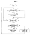
- FIG. 6 depicts a flowchart of one embodiment of a power control process carried out by the power control part 26.
- the power control part 26 determines in step S1 whether it is a normal operation timing. At a time of a normal operation time, the power control part 26 turns on SW1, SW2 and SW3 in step S2.
- step S3 determines in step S3 whether it is a non-operating timing of a stand-by operation. When it is not a non-operating timing, the power control part 26 proceeds with step S1. When it is a non-operating timing, the power control part 26 proceeds with step S4.
- step S4 the power control part 26 determines whether a non-operating time T of an intermittent operation notified by a host apparatus exceeds a threshold ⁇ .
- the threshold corresponds to a non-operating time in which the total consumed current in the case where the a ratio of times of non-operating/operating is small according to the present invention becomes equal to the total consumed current in the case where the a ratio of times of non-operating/operating is large according to the present invention.
- the power control part 26 turns off SW1 and SW2 in step S5, and carries out retention of the processor block 21.
- the power control part 26 turns off SW1, SW2 and SW3 in step S6, and completely stops the processor block 21.
- FIG. 7 depicts a configuration diagram of a second embodiment of a processor block in a semiconductor integrated circuit according to the present invention. It is noted that a logical operation block 22 other than a processor has the same configuration as that in the first embodiment.
- the processor block 31 has a logic circuit part 31a and a memory 31b.
- the memory 31b has a sleep terminal 31c, and, when a sleep signal of the high level for example is supplied to the sleep terminal 31c, the memory 31b carries out retention and enters a sleep mode of power saving.
- a global power supply wire 23 supplies a power VDD1 of a voltage by which voltage the logic circuit parts and the memories in the LSI chip 20 can carry out a normal operation, for example, 1.2 V.
- a global power supply wire 24 supplies a power VSS of, for example, 0 V.
- a global power supply wire 25 supplies a power VDD2 of a voltage slightly higher than the lower limit voltage (for example, 0.9 V), for example, 1.0 V. By the lower limit voltage, the logic circuit parts and the memories can carry out a holding operation.
- Respective ones of n-channel MOS transistors SW2 through SW4 are turned on when a voltage higher than the power VDD1, for example, 3.3 V, to the gates.
- the power VDD2 is applied to the gate and drain of an n-channel MOS transistor SW0, and is turned on when a voltage between the gate and source V GS exceeds a threshold voltage V TH (for example, 0.1 V).
- a power control part 26 controls switching of turning on/off of SW2 through SW4.
- the MOS transistor SW2 supplies the power VDD1 to the logic circuit part 31a of the processor block 31 from the global power supply wire 23 when being turned on.
- the MOS transistor SW4 supplies the power VDD1 to the memory 31b of the processor block 31 from the global power supply wire 23 when being turned on.
- the global power supply wire 24 constantly supplies the power VSS to the logic circuit part 21a and the memory 21b of the processor block 21 and the logic circuit part 22a and the memory 22b of the logical operation block 22.
- the source of the MOS transistor SW0 is connected with the drain of the MOS transistor SW3, and thus the MOS transistors SW0 and SW3 are connected vertically.
- the MOS transistor SW2 is turned off and the MOS transistor SW3 is turned on, the power VDD2 is supplied from the global power supply wire 25 to the logic circuit part 31a of the processor block 31 with being dropped by a voltage of approximately 0.1 V by an on resistance of the MOS transistor SW0.
- the high level (3.3 V) is supplied to the gates of SW2 through SW4, and SW2 and SW4 are thus turned on.
- the voltage VDD1 (1.2 V) is supplied by which voltage a normal operation can be carried out.
- SW3 is also turned on.
- SW0 is turned off and the processor block 31 is cut off from the power VDD2.
- the low level (0 V) is supplied to the gate of SW2, the high level is supplied to SW3 and SW4, and the high level is supplied to the sleep terminal 31c.
- the lower limit voltage (0.9 V) by which voltage a holding operation can be carried out dropped by a voltage of approximately 0.1 V by an on resistance of the MOS transistor SW0, is supplied to the logic circuit part 31a of the processor block 31, and is maintained in a state in which a leak current is reduced. Further, the memory 31b carries out retention in the sleep mode.
- the low level (0 V) is supplied to the gates of SW2 through SW4 that are thus turned off, and thereby, the processor block 31 is completely cut off from the power VDD1 and the power VDD2, and completely stops (consumes 0 power).
- FIG. 8 depicts a configuration diagram of a third embodiment of a processor block in a semiconductor integrated circuit according to the present invention.
- a logical operation block 22 other than a processor has a configuration the same as that in the first embodiment.
- no global power supply wire 25 is provided in the third embodiment.
- a processor block 21 has a logic circuit part 21a and a memory 21b.
- a global power supply wire 23 supplies a power VDD1 of a voltage by which voltage the logic circuit parts and the memories in a LSI chip 20 can carry out a normal operation, for example, 1.2 V, a global power supply wire 24 supplies a power VSS of, for example, a voltage of 0 V, and no global power supply wire 25 is provided.
- Each of n-channel MOS transistors SW2 and SW3 is turned on when a voltage higher than the power VDD1, for example, 3.3 V, is applied to its gate.
- a power VDD2 is applied to a gate and a drain of an n-channel MOS transistor SW10 that is turned on when a voltage between the gate and the source, V GS exceeds a threshold V TH (for example, 0.3 V). Switching of turning on and off of each of SW2 and SW3 is controlled by a power control part 26.
- the MOS transistor SW2 supplies the power VDD1 to the logic circuit part 21a and the memory 21b of the processor block 21 from the global power supply wire 23 when being turned on.
- the MOS transistor SW3 supplies the power VDD1 to the logic circuit part 21a and the memory 21b of the processor block 21 from the global power supply wire 23 when being turned on.
- the global power supply wire 24 constantly supplies the power VSS to the logic circuit part 21a and the memory 21b of the processor block 21 and the logic circuit part 22a and the memory 22b of the logical operation block 22.
- the source of the MOS transistor SW10 is connected with the drain of the MOS transistor SW3, and thus the MOS transistors SW10 and SW3 are vertically connected.
- the global power supply line 23 supplies the power VDD1 to the logic circuit part 21a and the memory 22b of the processor block 21 with being dropped by a voltage of approximately 0.3 V by an on resistance of the MOS transistor SW10.
- a high level (3.3 V) is supplied to the gates of SW2 and SW3, SW2 is turned on, and thereby, the voltage VDD1 (1.2 V) by which voltage a normal operation can be carried out is supplied to the processor block 21.
- SW3 is also turned on.
- SW10 is turned off because a source voltage of the MOS transistor SW10 is 1.2 V, and the voltage between the gate and the source V GS is less than the threshold V TH .
- a low level (0 V) is supplied to the gate of SW2, and the high level is supplied to the gate of SW3.
- a lower limit voltage (0.9 V) by which voltage a holding operation can be carried out is supplied to the logic circuit part 21a and the memory 21b of the processor 21 with being dropped by a voltage of approximately 0.3 V by an on resistance of the MOS transistor SW10, and a state is held in which a leak current is reduced.
- the low level (0 V) is supplied to the gates of SW2 and SW3 that are thus turned off, and thereby, the processor block 21 is completely cut off from the power VDD1, and completely stops (consumes 0 power).
- FIG. 9 depicts a configuration diagram of a fourth embodiment of a processor block in a semiconductor integrated circuit according to the present invention. It is noted that a logical operation block 22 other than a processor has a configuration the same as that in the first embodiment.
- the fourth embodiment is different from the third embodiment in that SW2, SW3 and SW10 are provided to a power VSS that is a common voltage on a negative side.
- a processor block 21 has a logic circuit part 21a and a memory 21b.
- a global power supply wire 23 supplies a power VDD1 of a voltage by which voltage the logic circuit parts and the memories in a LSI chip 20 can carry out a normal operation, for example, 1.2 V, a global power supply wire 24 supplies a power VSS of a voltage, for example, 0 V, and no global power supply wire 25 is provided.
- Each of the n-channel MOS transistors SW2 and SW3 is turned on when a voltage higher than the power VDD1, for example, 3.3 V, is applied to its gate.
- a gate and a drain of the n-channel MOS transistor SW10 are connected to negative side power supply wires of the logic circuit part 21a and the memory 21b, the power VSS is applied to its drain, and is turned on when a voltage between its gate and source V GS exceeds a threshold V TH (for example, 0.3 V). Switching of turning on/off of SW2 and SW3 is controlled by a power control part 26.
- the MOS transistor SW2 supplies the power VSS to the logic circuit part 21a and the memory 21b of the processor block 21 when being turned on and being connected to the global power supply wire 24.
- the MOS transistor SW3 supplies the power VSS to the logic circuit part 21a and the memory 21b of the processor block 21 when being turned on and being connected to the global power supply wire 24.
- the global power supply wire 23 constantly supplies the power VDD1 to the logic circuit part 21a and the memory 21b of the processor block 21 and the logic circuit part 22a and the memory 22b of the logical operation block 22.
- a source of the MOS transistor SW10 is connected to a drain of the MOS transistor SW3, and thus the MOS transistors SW10 and SW3 are vertically connected.
- the MOS transistor SW2 is turned off and the MOS transistor SW3 is turned on, the power VDD1 from the global power wire 23 flows to the power VSS through the logic circuit part 21a and the memory 22b of the processor block 21 with being dropped by a voltage of approximately 0.3 V by an on resistance of the MOS transistor SW10.
- a high level (3.3 V) is supplied to the gates of SW2 and SW3, SW2 is turned on, and thus, a voltage VDD1 (1.2 V) by which voltage a normal operation can be carried out is supplied to the processor block 21.
- VDD1 1.2 V
- SW3 is also turned on.
- SW10 is turned off.
- a low level (0 V) is supplied to the gate of SW2, and the high level is supplied to the gate of SW3.
- a lower limit voltage (0.9 V) by which voltage a holding operation can be carried out is supplied to the logic circuit part 21a and the memory 21b of the processor block 21 with being dropped by a voltage of approximately 0.3 V by an on resistance of the MOS transistor SW10, and a state in which a leak current is reduced is held.
- the low level (0 V) is supplied to the gates of SW2 and SW3 that are turned off, and thus, the processor block 21 is completely cut off from the power VSS, and completely stops (consumes 0 power).
- FIG. 10 depicts a configuration diagram of a fifth embodiment of a processor block in a semiconductor integrated circuit according to the present invention. It is noted that a logical operation block 22 other than a processor has a configuration the same as that in the first embodiment.
- the fifth embodiment is different from the fourth embodiment in that SW2 is provided to a side of a power VDD1.
- a processor block 21 has a logic circuit part 21a and a memory 21b.
- a global power supply wire 23 supplies a power VDD1 of a voltage by which voltage the logic circuit parts and the memories in a LSI chip 20 can carry out a normal operation, for example, 1.2 V, a global power supply wire 24 supplies a power VSS of a voltage, for example, 0 V, and no global power supply wire 25 is provided.
- Each of the n-channel MOS transistors SW2 and SW3 is turned on when a voltage higher than the power VDD1, for example, 3.3 V, is applied to its gate.
- a gate and a drain of the n-channel MOS transistor SW10 are connected to negative side power supply wires of the logic circuit part 21a and the memory 21b, the power VSS is applied to its drain, and is turned on when a voltage between its gate and source V GS exceeds a threshold V TH (for example, 0.3 V). Switching of turning on/off of SW2 and SW3 is controlled by a power control part 26.
- the MOS transistor SW2 supplies the power VDD1 to the logic circuit part 21a and the memory 21b of the processor block 21 when being turned on and being connected to the global power supply wire 23.
- the MOS transistor SW3 supplies the power VSS to the logic circuit part 21a and the memory 21b of the processor block 21 when being turned on and being connected to the global power supply wire 24.
- a source of the MOS transistor SW10 is connected to the global power supply wire 23.
- the MOS transistor SW2 is turned off and the MOS transistor SW3 is turned on, the power VDD1 from the global power wire 23 flows to the power VSS through the logic circuit part 21a and the memory 22b of the processor block 21.
- a high level (3.3 V) is supplied to the gates of SW2 and SW3 that are turned on, and thus, a voltage VDD1 (1.2 V) by which voltage a normal operation can be carried out is supplied to the processor block 21.
- VDD1 1.2 V
- the high level is supplied to the gate of SW2, and a low level (0 V) is supplied to the gate of SW3.
- a lower limit voltage (0.9 V) is supplied to the logic circuit part 21a and the memory 21b of the processor block 21 with being dropped by a voltage of approximately 0.3 V by an on resistance of the MOS transistor SW10.
- a holding operation can be carried out. By doing so, a state in which a leak current is reduced is held.
- the low level (0 V) is supplied to the gates of SW2 and SW3 that are turned off, and thus, the processor block 21 is completely cut off from the power VSS, and completely stops (consumes 0 power).
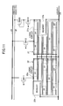
- FIG. 11 depicts a configuration diagram of a sixth embodiment of a semiconductor integrated circuit according to the present invention.
- the sixth embodiment is different from the first embodiment ( FIG. 2 ) in that p-channel MOS transistors SW11, SW12, SW13 and SW20 are used.
- a processor block 21 and a logical operation block 22 other than a processor are provided in an LSI chip 20, a processor block 21 and a logical operation block 22 other than a processor are provided.
- the processor block 21 has a logic circuit part 21a and a memory 21b.
- the logical operation block 22 has a logic circuit part 22a and a memory 22b.
- a global power supply wire 23 supplies a power VDD1 of a voltage by which voltage the logic circuit parts and the memories in the LSI chip 20 can carry out a normal operation, for example, 1.2 V
- a global power supply wire 24 supplies a power VSS of, for example, 0 V
- a global power supply wire 25 supplies a power VDD2 of a voltage slightly higher than a lower limit voltage (for example, 0.9 V) by which voltage the logic circuit parts and the memories can carry out a holding operation, for example, 1.0 V.
- Respective ones of the p-channel MOS transistors SW11 through SW13 are turned on when the power VSS (0 V) is applied to their gates, and are turned off when a voltage higher than the power VDD1, for example, 3.3 V, are applied to the gates.
- a gate and a drain of SW20 are connected with a source of SW13, and is turned on when a voltage between the gate and source V GS exceeds a threshold voltage V TH (for example, 0.1 V).
- a power control part 26 controls switching of turning on/off of SW11 through SW13.
- the MOS transistor SW11 supplies the power VDD1 to the logic circuit part 22a and the memory 22b of the logical operation block 22 from the global power supply wire 23 when being turned on.
- the MOS transistor SW12 supplies the power VDD1 to the logic circuit part 21a and the memory 21b of the processor block 21 from the global power supply wire 23 when being turned on.
- the global power supply wire 24 constantly supplies the power VSS to the logic circuit part 21a and the memory 21b of the processor block 21 and the logic circuit part 22a and the memory 22b of the logical operation block 22.
- the drain of the MOS transistor SW20 is connected with the source of the MOS transistor SW13, and thus the MOS transistors SW20 and SW13 are connected vertically.
- the MOS transistor SW12 is turned off and the MOS transistor SW13 is turned on, the power VDD2 is supplied from the global power supply wire 25 to the logic circuit part 21a and the memory 21b of the processor block 21 with being dropped by a voltage of approximately 0.1 V by an on resistance of the MOS transistor SW20.
- the global power supply wire 25 of the power VDD2 and the MOS transistor SW13 are provided only for holding in the processor block 21, it is possible to make the global power supply wire 25 thinner in comparison to the global power supply wire 23, it is possible to make a required area for the MOS transistor SW13 smaller in comparison to the MOS transistor SW12, and a remarkable increase in an area is required.
- a low level (0 V) is supplied to the gates of SW11, SW12 and SW13, and SW11 and SW12 are thus turned on.
- the voltage VDD1 1.2 V
- SW13 is also turned on.
- the drain voltage of the MOS transistor SW20 is 1.2 V, and the voltage between the gate and the source V GS is less than the threshold V TH , SW20 is turned off and the processor block 21 is cut off from the power VDD2.
- a high level (3.3 V) is supplied to the gates of SW11 and SW12 that are then turned off.
- the logical operation block 22 is completely cut off from the power VDD1, and the processor block 21 completely stops and consumes 0 power.
- the high level is supplied to the gates of SW11, SW12 and SW13 that are thus turned off, and thereby, the processor block 21 and the logical operation block 22 are completely cut off from the power VDD1 and the power VDD2, and completely stop (consume 0 power).
- SW1, SW2 and SW3 are turned on, and, the same as in an initial operation, a time of starting up of a reset operation in which, first, reading firmware is carried out, is required for the processor block 21.
- an operation time is sufficiently shorter than a non-operating time, the time of starting up can be ignored.
- FIG. 12 depicts a configuration diagram of a seventh embodiment of a processor block in a semiconductor integrated circuit according to the present invention.
- the seventh embodiment is different from the third embodiment ( FIG. 8 ) in that p-channel MOS transistors SW12, SW13 and SW30 are used. It is noted that, also for a logical operation block 22, a p-channel MOS transistor SW11 is used instead of SW1.
- a processor block 21 has a logic circuit part 21a and a memory 21b.
- a global power supply wire 23 supplies a power VDD1 of a voltage by which voltage the logic circuit parts and the memories in the LSI chip 20 can carry out a normal operation, for example, 1.2 V, a global power supply wire 24 supplies a power VSS of, for example, 0 V, and no global power supply wire 25 is provided.
- Respective ones of the n-channel MOS transistors SW12 and SW13 are turned on when the power VSS (0 V) is applied to their gates, and are turned off when a voltage higher than the power VDD1, for example, 3.3 V, are applied to the gates.
- a gate and a drain of SW30 are connected with a source of SW13, and is turned on when a voltage between the gate and source V GS exceeds a threshold voltage V TH (for example, 0.3 V).
- a power control part 26 controls switching of turning on/off of SW12 and SW13.
- the MOS transistor SW12 supplies the power VDD1 to the logic circuit part 21a and the memory 21b of the processor block 21 from the global power supply wire 23 when being turned on.
- the MOS transistor SW13 supplies the power VDD1 to the logic circuit part 21a and the memory 21b of the processor block 21 from the global power supply wire 23 when being turned on.
- the global power supply wire 24 constantly supplies the power VSS to the logic circuit part 21a and the memory 21b of the processor block 21 and the logic circuit part 22a and the memory 22b of the logical operation block 22.
- the drain of the MOS transistor SW30 is connected with the source of the MOS transistor SW3, and thus the MOS transistors SW30 and SW13 are connected vertically.
- the MOS transistor SW12 is turned off and the MOS transistor SW13 is turned on, the power VDD1 is supplied from the global power supply wire 23 to the logic circuit part 21a and the memory 22b of the processor block 21 with being dropped by a voltage of approximately 0.3 V by an on resistance of the MOS transistor SW30.
- a low level (0 V) is supplied to the gates of SW12 and SW13, and SW12 is turned on.
- the voltage VDD1 (1.2 V) is supplied to the processor block 21, by which voltage a normal operation can be carried out.
- SW13 is also turned on.
- the drain voltage of the MOS transistor SW30 is 1.2 V, and the voltage between the gate and the source V GS is less than the threshold V TH , SW30 is turned off.
- a high level (3.3 V) is supplied to the gates of SW12, and the low level is supplied to the gate of SW13.
- a lower limit voltage (0.9 V) is supplied to the logic circuit part 21a and the memory 21b of the processor block 21, dropped by a voltage of approximately 0.3 V by an on resistance of the MOS transistor SW30.
- a holding operation can be carried out.
- the logic circuit part 21a and the memory 21b of the processor block 21 are thus maintained in a state in which a leak current is reduced.
- the high level (3.3 V) is supplied to the gates of SW12 and SW13 that are thus turned off, and thereby, the processor block 21 is completely cut off from the power VDD1 and the power VDD2, and completely stop (consume 0 power).
- FIG. 13 depicts a configuration diagram of an eighth embodiment of a processor block in a semiconductor integrated circuit according to the present invention.
- the eighth embodiment is different from the fourth embodiment ( FIG. 9 ) in that p-channel MOS transistor SW30 is used.
- a processor block 21 has a logic circuit part 21a and a memory 21b.
- a global power supply wire 23 supplies a power VDD1 of a voltage by which voltage the logic circuit parts and the memories in the LSI chip 20 can carry out a normal operation, for example, 1.2 V, a global power supply wire 24 supplies a power VSS of, for example, 0 V, and no global power supply wire 25 is provided.
- Respective ones of n-channel MOS transistors SW2 and SW3 are turned on when a voltage higher than the power VDD1, for example, 3.3 V, is applied to their gates.
- a gate and a drain of the n-channel MOS transistor SW30 are connected to a negative side power supply wire of the logic circuit part 21a and the memory 21b, the power VSS is applied to its drain, and is turned on when a voltage between its gate and source V GS exceeds a threshold voltage V TH (for example, 0.3 V).
- a power control part 26 controls switching of turning on/off of SW2 and SW3.
- the MOS transistor SW2 supplies the power VSS to the logic circuit part 21a and the memory 21b of the processor block 21 when being turned on and being connected to the global power supply wire 24.
- the MOS transistor SW3 supplies the power VSS to the logic circuit part 21a and the memory 21b of the processor block 21 when being turned on and being connected to the power supply wire 24.
- the global power supply wire 23 constantly supplies the power VDD1 to the logic circuit part 21a and the memory 21b of the processor block 21 and the logic circuit part 22a and the memory 22b of the logical operation block 22.
- the source of the MOS transistor SW30 is connected with the drain of the MOS transistor SW3, and thus the MOS transistors SW30 and SW3 are connected vertically.
- the MOS transistor SW2 is turned off and the MOS transistor SW3 is turned on, the power VDD1 from the global power supply wire 23 flows to the power VSS through the logic circuit part 21a and the memory 22b of the processor block 21 with being dropped by a voltage of approximately 0.3 V by an on resistance of the MOS transistor SW30.
- a high voltage (3.3 V) is supplied to the gates of SW2 and SW3, and SW2 is turned on.
- the voltage VDD1 (1.2 V) is supplied to the processor block 21, by which voltage a normal operation can be carried out.
- SW3 is also turned on.
- SW30 is turned off.
- a low level (0 V) is supplied to the gate of SW2, and the high level is supplied to the gate of SW3.
- a lower limit voltage (0.9 V) is supplied to the logic circuit part 21a and the memory 21b of the processor block 21, dropped by a voltage of approximately 0.3 V by an on resistance of the MOS transistor SW30.
- a holding operation can be carried out.
- the logic circuit part 21a and the memory 21b of the processor block 21 are thus maintained in a state in which a leak current is reduced.
- the low level (0 V) is supplied to the gates of SW2 and SW3 that are thus turned off, and thereby, the processor block 21 is completely cut off from the power VSS, and completely stops (consumes 0 power).
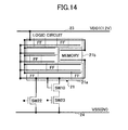
- FIG. 14 depicts a configuration diagram of a ninth embodiment of a processor block in a semiconductor integrated circuit according to the present invention.
- the ninth embodiment is different from the fourth embodiment ( FIG. 9 ) in that n-channel MOS transistors SW22 and SW23 having gates longer than that of an ordinary transistor that is turned on by a gate voltage of 1.2 V and thus having leak currents reduced to be the same as that of SW2 and SW3 are used instead of SW2 and SW3 that are turned on by a gate voltage of 3.3 V and have small leak currents.
- an n-channel MOS transistor SW21 the same as SW22 is used instead of SW1.
- a processor block 21 has a logic circuit part 21a and a memory 21b.
- a global power supply wire 23 supplies a power VDD1 of a voltage by which voltage the logic circuit parts and the memories in the LSI chip 20 can carry out a normal operation, for example, 1.2 V, a global power supply wire 24 supplies a power VSS of, for example, 0 V, and no global power supply wire 25 is provided.
- Respective ones of the n-channel MOS transistors SW22 and SW23 are turned on when 1.2 V is applied to their gates.
- a gate and a drain of an n-channel MOS transistor SW10 are connected to a negative side power supply wire of the logic circuit part 21a and the memory 21b, the power VSS is applied to its drain, and is turned on when a voltage between its gate and source V GS exceeds a threshold voltage V TH (for example, 0.3 V).
- a power control part 26 controls switching of turning on/off of SW22 and SW23.
- the MOS transistor SW22 supplies the power VSS to the logic circuit part 21a and the memory 21b of the processor block 21 when being turned on and being connected to the global power supply wire 24.
- the MOS transistor SW23 supplies the power VSS to the logic circuit part 21a and the memory 21b of the processor block 21 when being turned on and being connected to the power supply wire 24.
- the global power supply wire 23 constantly supplies the power VDD1 to the logic circuit part 21a and the memory 21b of the processor block 21 and the logic circuit part 22a and the memory 22b of the logical operation block 22.
- the source of the MOS transistor SW10 is connected with the drain of the MOS transistor SW23, and thus the MOS transistors SW10 and SW23 are connected vertically.
- the MOS transistor SW22 is turned off and the MOS transistor SW23 is turned on, the power VDD1 from the global power supply wire 23 flows to the power VSS through the logic circuit part 21a and the memory 22b of the processor block 21 and is dropped by a voltage of approximately 0.3 V by an on resistance of the MOS transistor SW10.
- a high voltage 1.2 V
- SW22 is turned on.
- the voltage VDD1 (1.2 V) by which voltage a normal operation can be carried out is supplied.
- SW23 is also turned on.
- SW10 is turned off.
- a low level (0 V) is supplied to the gate of SW22, and the high level is supplied to the gate of SW23.
- a lower limit voltage (0.9 V) dropped by a voltage of approximately 0.3 V by an on resistance of the MOS transistor SW10, by which voltage a holding operation can be carried out, is supplied, and the logic circuit part 21a and the memory 21b of the processor block 21 are maintained in a state in which a leak current is reduced.
- the low level (0 V) is supplied to the gates of SW22 and SW23 that are thus turned off, and thereby, the processor block 21 is completely cut off from the power VSS, and completely stops (consumes 0 power).
- FIG. 15 depicts a configuration diagram of a tenth embodiment of a processor block in a semiconductor integrated circuit according to the present invention. It is noted that, a logical operation block 22 other than a processor is the same as that in the first embodiment. The tenth embodiment is different from the fifth embodiment ( FIG.
- a processor block 21 has a logic circuit part 21a and a memory 21b.
- a global power supply wire 23 supplies a power VDD1 of a voltage by which voltage the logic circuit parts and the memories in the LSI chip 20 can carry out a normal operation, for example, 1.2 V, a global power supply wire 24 supplies a power VSS of, for example, 0 V, and no global power supply wire 25 is provided.
- the p-channel MOS transistors SW32 is turned off when 1.2 V is applied to its gate, and the n-channel MOS transistor S33 is turned on when 1.2 V is applied to its gate.
- a gate and a drain of an n-channel MOS transistor SW10 are connected to a negative side power supply wire of the logic circuit part 21a and the memory 21b, the power VSS is applied to its drain, and is turned on when a voltage between its gate and source V GS exceeds a threshold voltage V TH (for example, 0.3 V).
- a power control part 26 controls switching of turning on/off of SW32 and SW33.
- the MOS transistor SW32 supplies the power VDD1 to the logic circuit part 21a and the memory 21b of the processor block 21 when being turned on and being connected to the global power supply wire 23.
- the MOS transistor SW33 supplies the power VSS to the logic circuit part 21a and the memory 21b of the processor block 21 when being turned on and being connected to the power supply wire 24.
- the source of the MOS transistor SW10 is connected to the global power supply wire 23, and when the MOS transistor SW32 is turned off and the MOS transistor SW33 is turned on, the power VDD1 from the global power supply wire 23 flows to the power VSS through the logic circuit part 21a and the memory 22b of the processor block 21.
- a low voltage (0 V) is supplied SW32 and a high level (1.2 V) is supplied to the gate of SW3, and SW32 and SW33 are turned on.
- the voltage VDD1 (1.2 V) is supplied by which voltage a normal operation can be carried out.
- SW10 is turned off.
- the low level is supplied to the gate of SW32, and the low level (0 V) is supplied to the gate of SW33.
- a lower limit voltage (0.9 V) dropped by a voltage of approximately 0.3 V by an on resistance of the MOS transistor SW10, by which voltage a holding operation can be carried out, is supplied, and the logic circuit part 21a and the memory 21b of the processor block 21 are maintained in a state in which a leak current is reduced.
- the processor block 21 is completely cut off from the power VSS, and completely stops (consumes 0 power).
- FIG. 16 depicts a configuration diagram of an eleventh embodiment of a processor block in a semiconductor integrated circuit according to the present invention. It is noted that, a logical operation block 22 other than a processor is the same as that in the first embodiment. The eleventh embodiment is different from the fifth embodiment ( FIG. 10 ) in that p-channel MOS transistors SW12 and SW30 are used. It is noted that, also for a logical operation block 22, a p-channel MOS transistor SW11 is used instead of SW1.
- a processor block 21 has a logic circuit part 21a and a memory 21b.
- a global power supply wire 23 supplies a power VDD1 of a voltage by which voltage the logic circuit parts and the memories in the LSI chip 20 can carry out a normal operation, for example, 1.2 V, a global power supply wire 24 supplies a power VSS of, for example, 0 V, and no global power supply wire 25 is provided.
- the p-channel MOS transistors SW12 is turned off when 3.3 V is applied to its gate, and the n-channel MOS transistor S3 is turned on when 3.3 V is applied to its gate.
- a gate and a drain of an n-channel MOS transistor SW30 are connected to a source of SW13, and is turned on when a voltage between its gate and source V GS exceeds a threshold voltage V TH (for example, 0.3 V).
- a power control part 26 controls switching of turning on/off of SW3 and SW12.
- the MOS transistor SW12 supplies the power VDD1 to the logic circuit part 21a and the memory 21b of the processor block 21 when being turned on and being connected to the global power supply wire 23.
- the MOS transistor SW3 supplies the power VSS to the logic circuit part 21a and the memory 21b of the processor block 21 when being turned on and being connected to the power supply wire 24.
- the source of the MOS transistor SW30 is connected to the global power supply wire 23, and when the MOS transistor SW12 is turned off and the MOS transistor SW3 is turned on, the power VDD1 from the global power supply wire 23 flows to the power VSS through the logic circuit part 21a and the memory 22b of the processor block 21.
- a low voltage (0 V) is supplied SW12 and a high level (3.3 V) is supplied to the gate of SW3, and SW12 and SW3 are turned on.
- the voltage VDD1 1.2 V
- SW30 is turned off.
- the low level is supplied to the gate of SW12, and the low level is supplied to the gate of SW3.
- a lower limit voltage (0.9 V)
- a voltage of approximately 0.3 V by an on resistance of the MOS transistor SW30, by which voltage a holding operation can be carried out is supplied, and the logic circuit part 21a and the memory 21b of the processor block 21 are maintained in a state in which a leak current is reduced.
- the processor block 21 is completely cut off from the power VSS, and completely stops (consumes 0 power).
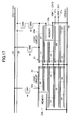
- FIG. 17 depicts a configuration diagram of a twelfth embodiment of a semiconductor integrated circuit according to the present invention.
- a processor block 21 and a logical operation block 22 other than a processor are provided in a LSI chip 20.
- the processor block 21 has a logic circuit part 21a and a memory 21b
- the logical operation block 22 includes a logic circuit part 22a and a memory 22b.
- VBP is a back bias voltage to be applied to p-channel wells
- VBN is a back bias voltage to be applied to n-channel wells.
- a global power supply wire 23 supplies a power VDD1 of a voltage by which voltage the logic circuit parts and the memories in the LSI chip 20 can carry out a normal operation, for example, 1.2 V
- a global power supply wire 24 supplies a power VSS of, for example, 0 V
- a global power supply wire 25 supplies a voltage VDD2 that is slightly higher than a lower limit voltage (for example, 0.9 V), by which voltage the logical circuit parts and the memories can carry out a holding operation, for example, 1.0 V.
- Respective ones of n-channel transistors SW1 through SW3 are transistors that are turned on when a voltage that is higher than the power VDD1, for example, 3.3 V, is applied to their gates. Therefore, it is possible to reduce leak currents of SW1 through SW3 when a voltage 0 V is applied to the gates to be lower in comparison to a normal transistor that is turned on by a gate voltage of 1.2V.
- a power control part 26 controls switching of turning on/off of SW1 through SW3.
- the power VDD2 is applied to a gate and a drain of the n-channel MOS transistor SW0, and is turned on when a voltage V GS between the gate and a source exceeds a threshold voltage V TH (for example, 0.1 V).
- the MOS transistor SW1 supplies the power VDD1 to the logic circuit part 22a and the memory 22b of the logical operation block 22 from the power supply wire 23 when being turned on.
- the MOS transistor SW2 supplies the power VDD1 to the logic circuit part 21a and the memory 21b of the processor block 21 from the power supply wire 23 when being turned on.
- the global power supply wire 24 constantly supplies the power VSS to the logic circuit part 21a and the memory 21b of the processor block 21 and the logical circuit part 22a and the memory 22b of the logical operation block 22.
- the source of the MOS transistor SW0 is connected to the drain of the MOS transistor SW3, and SW0 and SW3 are vertically connected.
- the MOS transistor SW2 is turned off and the MOS transistor SW3 is turned on, the power VDD2 is supplied to the logic circuit part 21a and the memory 21b of the processor block 21 from the global power supply wire 25 with being dropped by a voltage of approximately 0.1 V by an on resistance of the MOS transistor SW0
- a high voltage is supplied to the gates of SW1 through SW4, SW2 and SW4 are turned on, and, to the processor block 21, the voltage VDD1 (1.2 V) by which voltage a normal operation can be carried out is supplied.
- SW3 is turned on.
- the source voltage of the MOS transistor SW0 is 1.2 V, and the voltage between the gate and the source V GS is less than the threshold V TH , SW0 is turned off. Therefore, the processor block 21 is cut off from the power VDD2.
- a low level (0 V) is supplied to the gate of SW2, the high level is supplied to the gates of SW3 and SW4, and VPN > 1.2 V and VBN ⁇ 0 V are supplied to the terminals 21c and 21d.
- a lower limit voltage (0.9 V) to the processor block 21 dropped by a voltage of approximately 0.1 V by an on resistance of the MOS transistor SW0.
- a holding operation can be carried out, is supplied.
- the processor block 21 is thus maintained in a state in which a leak current is reduced.
- VBP > 1.2V and VBN ⁇ 0 V being supplied to the terminals 21c and 21d, it is possible to further reduce the leak current in the logic circuit part 21a of the processor block 21.
- the low level (0 V) is supplied to the gates of SW1 through SW4 that are then turned off, and thereby, the logical operation block 22 and the processor block 21 are completely cut off from the power VDD1 and the power VDD2, and completely stop (consume 0 power).
- the MOS transistor SW2 is used as an example of second switching means
- the MOS transistor SW3 is used as an example of third switching means
- the MOS transistor SW0 is used as an example of fourth switching means.
Landscapes
- Engineering & Computer Science (AREA)
- Physics & Mathematics (AREA)
- General Engineering & Computer Science (AREA)
- Theoretical Computer Science (AREA)
- General Physics & Mathematics (AREA)
- Computer Hardware Design (AREA)
- Computing Systems (AREA)
- Mathematical Physics (AREA)
- Semiconductor Integrated Circuits (AREA)
- Power Sources (AREA)
- Microcomputers (AREA)
- Logic Circuits (AREA)
Abstract
Description
- The present invention relates to a semiconductor integrated circuit, and to a semiconductor integrated circuit that has a processor block and an logical operation block other than a processor, and carries out an intermittent operation.
- For a system LSI (Large Scale Integrated circuit) for a portable information terminal such as a cellular phone, a global clock gating technique, and a power gating technique are provided as a technology for achieving long time driving by using a battery.
- The global clock gating technique is such that, in a non-operating time of an intermittent operation (stand-by operation), distribution clock signals to unnecessary blocks are stopped so that an operating current is reduced to a leak level.
- The power gating technique is such that, further a power supply line to each block is previously separated, and a switch for each power supply line provided outside of a semiconductor chip or inside of the semiconductor chip is turned off, so that a leak current of the block is also reduced.
- For the future, to save power consumption by using on-chip power gating technique becomes a main current in view of a miniaturization of transistors along with technology improvement, an increase in a leak current which becomes unignorable because of an increase in circuit size that is mounted, and a power-off switching speed.
- It is noted that Patent Document 1 describes providing processors in a plurality of functional circuit blocks so that they can operate independently, providing a system state transition resistor and a power-off register, controlling the registers by an external computer, and controlling power-off separately for the functional circuit blocks that are in an operation stop state.
- Patent Document 1: Japanese Laid-Open Patent Publication No.
2003-114742 - When a power supply is turned off during an intermittent operation (stand-by operation), a situation in a recovering operation is very different between a processor that operates by firmware and another processing circuit. In a case where a power supply to a processor is turned off, a problem occurs in recovering to a normal operating (transmitting/receiving operation). When a consideration is not carried out upon turning off a power supply, a time is required in recovery because, the same as an initialization operation, a firmware is read from an external memory, and a reset operation for starting up the firmware in sequence is required.
- As a result, a time for which a power supply is turned off is reduced. Further, a method may be considered in which, before turning off, the contents of a memory or flip-flops of a processor is saved in a RAM or such outside of an LSI, and, in recovery, the contents are read from the RAM or such outside of the LSI in the memory or the flip-flops reversely. However, a firmware should be developed for achieving complicate operations.
-
FIG. 1 depicts one example of a configuration diagram of a prior-art semiconductor integrated circuit for solving this. In the same figure, in aLSI chip 10, aprocessor block 11 and alogical operation block 12 other than theprocessor block 11 are provided. - The
processor block 11 includes a logic circuit part l1a and a memory 11b, power VDD (1.2 V) and VSS are constantly supplied to thelogic circuit part 11a from globalpower supply wires power supply wires - The
logical operation block 12 includes alogic circuit part 12a and amemory 12b, and power VDD (1.2 V) and VSS are constantly supplied to thelogic circuit part 12a and thememory 12b only when a MOS transistor SW is turned on. - That is, such a method has been a main current that, the power VDD is separated for the
processor block 11 and thelogical operation block 12 other than theprocessor block 11, the power VDD for thelogical operation block 12 is not turned off during an intermittent operation, a retention is carried out only for the memory 11b such that the power VDD is reduced from 1.2 V to 0.9 V that is a lowest voltage for being able to hold data, and thus, an electric current is reduced. - Ordinarily, there is a tendency that the
processor block 11 is required to have the highest processing speed in a chip, also the logic circuit uses high-speed transistors that have larger leak currents, and, when a time of turning off is long, a leak current reducing effect decreases in theLSI chip 10 in total. It is noted that high-speed transistors have short gate lengths, and thus, have large leak currents. - As a countermeasure, in order to control a leak current of the
logic circuit part 11a in theprocessor block 11 as much as possible, a scheme may be considered such that a power source is separated for storage circuits such as flip-flops, and other gate logic circuits, and a power supply only the logic gate circuits is selectively turned off. However, in an actual layout, flip-flops are, functionally, disposed in a scattered manner, and thus, it is difficult to physically carry out power supply separation. If power supply separation is carried out nevertheless, problematically an area increases. - Further, another scheme may be considered such that data in flip-flops is saved in other built-in flip-flops provided for the purpose holding the data. However, problematically, a complication occurs in a recovery operation and an area increases.
- The present invention has been devised in consideration of the above-mentioned points, and a general object of the present invention is to reduce a leak current, and provide a semiconductor integrated circuit that achieves a plurality of recovering modes, without a remarkable increase in an area.
- In order to achieve the object, a semiconductor integrated circuit according to the present invention has, in a semiconductor integrated circuit having a processor block and an logical operation block other than a processor, and carrying out an intermittent operation, first switch means for supplying a normal operation voltage to the logical operation block other than a processor; second switch means for supplying the normal operation voltage to the processor block; third switch means for supplying a data holding voltage lower than the normal operation voltage to the processor block; and fourth switch means for being turned on, when the second switch means is turned off and the third switch means is turned on, and supplying the data holding voltage to the processor block.
- By the semiconductor integrated circuit, it is possible to reduce a leak current, and to achieve a plurality of recovering modes without remarkably increasing an area.
-
-
FIG. 1 is a configuration diagram of one example of a prior-art semiconductor integrated circuit. -
FIG. 2 is a configuration diagram of a first embodiment of a semiconductor integrated circuit according to the present invention. -
FIG. 3 is a diagram depicting a ratio of a consumed current of each circuit. -
FIG. 4 is a diagram depicting a ratio of a time of non-operating/operating. -
FIG. 5 is a diagram depicting a ratio of a total consumed current. -
FIG. 6 is a flowchart of one embodiment of a power control process. -
FIG. 7 is a configuration diagram of a second embodiment of a processor block. -
FIG. 8 is a configuration diagram of a third embodiment of a processor block. -
FIG. 9 is a configuration diagram of a fourth embodiment of a processor block. -
FIG. 10 is a configuration diagram of a fifth embodiment of a processor block. -
FIG. 11 is a configuration diagram of a sixth embodiment of a semiconductor integrated circuit according to the present invention. -
FIG. 12 is a configuration diagram of a seventh embodiment of a processor block. -
FIG. 13 is a configuration diagram of an eighth embodiment of a processor block. -
FIG. 14 is a configuration diagram of a ninth embodiment of a processor block. -
FIG. 15 is a configuration diagram of a tenth embodiment of a processor block. -
FIG. 16 is a configuration diagram of an eleventh embodiment of a processor block. -
FIG. 17 is a configuration diagram of a twelfth embodiment of a semiconductor integrated circuit according to the present invention. -
- 20
- LSI chip
- 21
- processor block
- 22
- logical operation block
- 21a, 22a
- logic circuit part
- 21b, 22b
- memory
- 23
- through 25 global power supply wire
- 26
- power control part
- SW1 through SW30
- MOS transistor
- Below, based on figures, embodiments of the present invention will be described.
-
FIG. 2 depicts a configuration diagram of a first embodiment of a semiconductor integrated circuit according to the present invention. In the figure, in aLSI chip 20 that is a system LSI for a portable information terminal for example, aprocessor block 21 and alogical operation block 22 other than a processor are provided. Further, in theLSI chip 20, apower control part 26 is provided. - The
processor block 21 has alogic circuit part 21a and amemory 21b, and thelogical operation block 22 has alogic circuit part 22b and amemory 22b. - A global
power supply wire 23 supplies a power VDD1 of a voltage by which voltage the logic circuit parts and the memories in theLSI chip 20 can carry out a normal operation, for example, 1.2 V, a globalpower supply wire 24 supplies a power VSS of, for example, 0 V, and a globalpower supply wire 25 supplies a power VDD2 of a voltage that is slightly higher than the lower limit voltage (for example, 0.9 V) by which voltage the logical circuit parts and the memories in theLSI chip 20 can carry out a holding operation, for example, 1.0 V. - N-channel MOS transistors SW1 through SW3 are transistors that are turned on when a voltage higher than the power VDD1, for example, 3.3 V, is applied to gates, respectively. Therefore, it is possible to reduce leak currents occurring when a voltage of 0 V is applied to SW1 through SW3 that are then turned off, in comparison to ordinary transistors that are turned on by a gate voltage of 1.2 V. Switching of turning on/off of SW1 through SW3 is controlled by the
power control part 26. - The power VDD2 is applied to a gate and a drain of the n-channel MOS transistor SW0, which is turned on when a voltage VGS between the gate and a source exceeds a threshold voltage VTH (for example, 0.1 V).
- When being turned on, the MOS transistor SW1 supplies from the global
power supply wire 23 the power VDD1 to thelogic circuit part 22a and thememory 22b of thelogical operation block 22. When being turned on, the MOS transistor SW2 supplies from the globalpower supply wire 23 the power VDD1 to thelogic circuit part 21a and thememory 21b of theprocessor block 21. - It is noted that the global
power supply wire 24 constantly supplies the power VSS to thelogic circuit part 21a and thememory 21b of theprocessor block 21 and thelogic circuit part 22a and thememory 22b of thelogical operation block 22. - The source of the MOS transistor SW0 is connected with the drain of the MOS transistor SW3, thus the MOS transistors SW0 and SW3 are vertically connected. When the MOS transistor SW2 is turned off and the MOS transistor SW3 is turned on, the power VDD2 from the global
power supply wire 25 is dropped by a voltage of approximately 0.1 V through an on resistance of the MOS transistor SW0, to be applied to thelogic circuit part 21a and thememory 21b of theprocessor block 21. - The global
power supply wire 25 of the power VDD2 and the MOS transistor SW3 are used only for a holding purpose in theprocessor block 21. Therefore, it is possible to reduce a size of the globalpower supply wire 25 in comparison to the globalpower supply wire 23, and an area for the MOS transistor SW3 can be made smaller than that of the MOS transistor SW2. Therefore, the globalpower supply wire 25 of the power VDD2 and the MOS transistor SW3 do not require a remarkably large increased in an area. - (1) At a time of a normal operation (at a time of transmitting and receiving mode):
- To the gates of SW1, SW2 and SW3, the high level (3.3 V) is supplied, SW1 and SW2 are turned on, thereby VDD1 (1.2 V) by which voltage a normal operation can be carried out is supplied to the
processor block 21 and thelogical operation block 22. At this time, SW3 is also turned on. However, theprocessor block 21 is cut off from the power VDD2 because a source voltage of the MOS transistor SW0 is 1.2 V, a voltage between the gate and source VGS is lower than the threshold voltage VTH, and SW0 is turned off.
Another configuration may be considered in which the power VDD is 0.9 V and SW0 is not provided. However, in this case, it is necessary to carry out switching of turning on/off of SW2 and switching of turning on/off of SW2 completely simultaneously. It is difficult and thus is not practical to so completely simultaneously carry out switching operations of SW2 and SW3. - To the gates of SW1, SW2 and SW3, the high level (3.3 V) is supplied, SW1 and SW2 are turned on, thereby VDD1 (1.2 V) by which voltage a normal operation can be carried out is supplied to the
- (2) At a time of intermittent operation (at a time of a stand-by operation):
- (2-1) At a time of high-speed recovery (without a reset operation) being required:
- At a time of non-operating (at a time of a stand-by operation), the low level (0 V) is supplied to the gates of SW1 and SW2 that are thus turned off, and thereby, the
logical operation block 22 is completely cut off from the power VDD1, and thelogical operation block 22 completely stops and consumes no power. - However, the high level (3.3 V) is supplied to the gate of SW3 that is thus still turned on. Therefore, the lower limit voltage (0.9 V) by which voltage a holding operation can be carried out is supplied to the
processor block 21, and retention is carried out in which a holding operation is carried out while a leak current is reduced. - At a time of recovery, only it is necessary to turn on SW1 and SW2, reading of firmware is not necessary, and the
processor block 21 can be recovered at a high speed.
- At a time of non-operating (at a time of a stand-by operation), the low level (0 V) is supplied to the gates of SW1 and SW2 that are thus turned off, and thereby, the
- (2-2) At a time of a non-operating time being long and a high-speed recovery being not required (with a reset operation):
- At a time of non-operating (at a time of a stand-by operation), the low level (0 V) is supplied to the gates of SW1, SW2 and SW3 that are thus turned off, and thereby, the
processor block 21 and thelogical operation block 22 are completely cut off from the power VDD1 and the power VDD2, and completely stop (consume no power).
At a time of recovery, SW1, SW2 and SW3 are turned on, and, a time of starting up a reset operation (approximately a fixed time) in which an operation of reading firmware and a following operation are carried out is required, same as an initial operation, in theprocessor block 21. However, because an operating time is sufficiently shorter than a non-operating time, the starting up time may be ignored. - At a time of non-operating (at a time of a stand-by operation), the low level (0 V) is supplied to the gates of SW1, SW2 and SW3 that are thus turned off, and thereby, the
- (2-1) At a time of high-speed recovery (without a reset operation) being required:
- In an intermittent operation (a stand-by operation) in a cellular phone, a non-operating time T (in which a power supply is broken) varies in a range of several tens of milliseconds through several seconds. However, a time of stating up a reset operation (for example, several milliseconds through several tens of milliseconds) and an operating time (for example, several milliseconds through several tens of milliseconds) are fixed and do not vary.
- It is assumed that the
processor block 21 occupies 1/10 times in a circuit size, consumes 1.5 times in an operating current and consumes 10 times in a leak current with respect to the other plural logical operation blocks 22. In this case, it is assumed that consumed current values of respective ones of thelogic circuit parts 22a and thememories 22b, and thelogic circuit part 21a and thememory 21b of theprocessor block 21, have ratios as depicted inFIG. 3 at a time of operation (Active), a time of a stand-by operation (Stand by), a time of retention, a time of non-operating (Off), and a time of reset (Reset). It is noted that a current at the time of a stand-by operation denotes a leak current. - Further, ratios of respective time lengths of a time of operating (Active), a time of stand-by or retention or non-operating (Off) and a time of reset (Reset) in a case where a ratio of times of non-operating/operating is small and a reset operation is not carried out; a case where a ratio of times of non-operating/operating is small and a reset operation is carried out; a case where a ratio of times of non-operating/operating is large and a reset operation is not carried out; and a case where a ratio of times of non-operating/operating is large and a reset operation is not carried out, are depicted in
FIG. 4 . - From the respective conditions depicted in
FIGS. 3 and 4 , a ratio of total consumed currents in a case where a ratio of times of non-operating/operating is small and a reset operation is not carried out in the prior art is 4.78 as depicted inFIG. 5 . A ratio of total consumed currents in a case where a ratio of times of non-operating/operating is large and a reset operation is not carried out is 0.27. An average thereof is 2.52. - A ratio of total consumed currents in a case where a ratio of times of non-operating/operating is small and a reset operation is carried out in the prior art is 11.50 as depicted in
FIG. 5 . A ratio of total consumed currents in a case where a ratio of times of non-operating/operating is large and a reset operation is carried out is 0.12. An average thereof is 5.81. - In comparison thereto, according to the present invention, a ratio of total consumed currents in a case where a ratio of times of non-operating/operating is small and a reset operation is not carried out is 3.29. A ratio of total consumed currents in a case where a ratio of times of non-operating/operating is large and a reset operation is carried out is 0.12. An average thereof is 1.17.
- That is, where a reset operation is not carried out at all, a consumed current reduction effect of the present invention is approximately 1.5 times the prior art. The consumed current reduction effect of the present invention is approximately 3.4 times with respect to the prior-art circuit where a reset operation is necessarily carried out.
-
FIG. 6 depicts a flowchart of one embodiment of a power control process carried out by thepower control part 26. In the figure, thepower control part 26 determines in step S1 whether it is a normal operation timing. At a time of a normal operation time, thepower control part 26 turns on SW1, SW2 and SW3 in step S2. - Next, the
power control part 26 determines in step S3 whether it is a non-operating timing of a stand-by operation. When it is not a non-operating timing, thepower control part 26 proceeds with step S1. When it is a non-operating timing, thepower control part 26 proceeds with step S4. - In step S4, the
power control part 26 determines whether a non-operating time T of an intermittent operation notified by a host apparatus exceeds a threshold τ. The threshold corresponds to a non-operating time in which the total consumed current in the case where the a ratio of times of non-operating/operating is small according to the present invention becomes equal to the total consumed current in the case where the a ratio of times of non-operating/operating is large according to the present invention. - When the non-operating time T is equal to or less than the threshold τ, the non-operating time is small and a high-speed recovery is required (without a reset operation). Therefore, the
power control part 26 turns off SW1 and SW2 in step S5, and carries out retention of theprocessor block 21. - When the non-operating time T exceeds the threshold τ, the non-operating time is large and a high-speed recovery is not required (with a reset operation). Therefore, the
power control part 26 turns off SW1, SW2 and SW3 in step S6, and completely stops theprocessor block 21. -
FIG. 7 depicts a configuration diagram of a second embodiment of a processor block in a semiconductor integrated circuit according to the present invention. It is noted that alogical operation block 22 other than a processor has the same configuration as that in the first embodiment. - In the figure, the
processor block 31 has alogic circuit part 31a and amemory 31b. Thememory 31b has asleep terminal 31c, and, when a sleep signal of the high level for example is supplied to thesleep terminal 31c, thememory 31b carries out retention and enters a sleep mode of power saving. - A global
power supply wire 23 supplies a power VDD1 of a voltage by which voltage the logic circuit parts and the memories in theLSI chip 20 can carry out a normal operation, for example, 1.2 V. A globalpower supply wire 24 supplies a power VSS of, for example, 0 V. A globalpower supply wire 25 supplies a power VDD2 of a voltage slightly higher than the lower limit voltage (for example, 0.9 V), for example, 1.0 V. By the lower limit voltage, the logic circuit parts and the memories can carry out a holding operation. - Respective ones of n-channel MOS transistors SW2 through SW4 are turned on when a voltage higher than the power VDD1, for example, 3.3 V, to the gates. The power VDD2 is applied to the gate and drain of an n-channel MOS transistor SW0, and is turned on when a voltage between the gate and source VGS exceeds a threshold voltage VTH (for example, 0.1 V). A
power control part 26 controls switching of turning on/off of SW2 through SW4. - The MOS transistor SW2 supplies the power VDD1 to the
logic circuit part 31a of theprocessor block 31 from the globalpower supply wire 23 when being turned on. The MOS transistor SW4 supplies the power VDD1 to thememory 31b of theprocessor block 31 from the globalpower supply wire 23 when being turned on. - It is noted that the global
power supply wire 24 constantly supplies the power VSS to thelogic circuit part 21a and thememory 21b of theprocessor block 21 and thelogic circuit part 22a and thememory 22b of thelogical operation block 22. - The source of the MOS transistor SW0 is connected with the drain of the MOS transistor SW3, and thus the MOS transistors SW0 and SW3 are connected vertically. When the MOS transistor SW2 is turned off and the MOS transistor SW3 is turned on, the power VDD2 is supplied from the global
power supply wire 25 to thelogic circuit part 31a of theprocessor block 31 with being dropped by a voltage of approximately 0.1 V by an on resistance of the MOS transistor SW0. - At a time of a normal operation, the high level (3.3 V) is supplied to the gates of SW2 through SW4, and SW2 and SW4 are thus turned on. Thereby, to the
processor block 31, the voltage VDD1 (1.2 V) is supplied by which voltage a normal operation can be carried out. At this time, SW3 is also turned on. However, because the source voltage of the MOS transistor SW0 is 1.2 V and the voltage between the gate and the source VGS is less than the threshold VTH, SW0 is turned off and theprocessor block 31 is cut off from the power VDD2. - At a time of non-operating (without a reset operation), the low level (0 V) is supplied to the gate of SW2, the high level is supplied to SW3 and SW4, and the high level is supplied to the
sleep terminal 31c. Thereby, the lower limit voltage (0.9 V) by which voltage a holding operation can be carried out, dropped by a voltage of approximately 0.1 V by an on resistance of the MOS transistor SW0, is supplied to thelogic circuit part 31a of theprocessor block 31, and is maintained in a state in which a leak current is reduced. Further, thememory 31b carries out retention in the sleep mode. - Further, at a time of non-operating (with a reset operation), the low level (0 V) is supplied to the gates of SW2 through SW4 that are thus turned off, and thereby, the
processor block 31 is completely cut off from the power VDD1 and the power VDD2, and completely stops (consumes 0 power). -
FIG. 8 depicts a configuration diagram of a third embodiment of a processor block in a semiconductor integrated circuit according to the present invention. Alogical operation block 22 other than a processor has a configuration the same as that in the first embodiment. In the third embodiment, no globalpower supply wire 25 is provided. - In the figure, a
processor block 21 has alogic circuit part 21a and amemory 21b. A globalpower supply wire 23 supplies a power VDD1 of a voltage by which voltage the logic circuit parts and the memories in aLSI chip 20 can carry out a normal operation, for example, 1.2 V, a globalpower supply wire 24 supplies a power VSS of, for example, a voltage of 0 V, and no globalpower supply wire 25 is provided. - Each of n-channel MOS transistors SW2 and SW3 is turned on when a voltage higher than the power VDD1, for example, 3.3 V, is applied to its gate. A power VDD2 is applied to a gate and a drain of an n-channel MOS transistor SW10 that is turned on when a voltage between the gate and the source, VGS exceeds a threshold VTH (for example, 0.3 V). Switching of turning on and off of each of SW2 and SW3 is controlled by a
power control part 26. - The MOS transistor SW2 supplies the power VDD1 to the
logic circuit part 21a and thememory 21b of theprocessor block 21 from the globalpower supply wire 23 when being turned on. The MOS transistor SW3 supplies the power VDD1 to thelogic circuit part 21a and thememory 21b of theprocessor block 21 from the globalpower supply wire 23 when being turned on. - It is noted that the global
power supply wire 24 constantly supplies the power VSS to thelogic circuit part 21a and thememory 21b of theprocessor block 21 and thelogic circuit part 22a and thememory 22b of thelogical operation block 22. - The source of the MOS transistor SW10 is connected with the drain of the MOS transistor SW3, and thus the MOS transistors SW10 and SW3 are vertically connected. When the MOS transistor SW2 is turned off and the MOS transistor SW3 is turned on, the global
power supply line 23 supplies the power VDD1 to thelogic circuit part 21a and thememory 22b of theprocessor block 21 with being dropped by a voltage of approximately 0.3 V by an on resistance of the MOS transistor SW10. - At a time of a normal operation, a high level (3.3 V) is supplied to the gates of SW2 and SW3, SW2 is turned on, and thereby, the voltage VDD1 (1.2 V) by which voltage a normal operation can be carried out is supplied to the
processor block 21. At this time, SW3 is also turned on. However, SW10 is turned off because a source voltage of the MOS transistor SW10 is 1.2 V, and the voltage between the gate and the source VGS is less than the threshold VTH. - At a time of non-operating (without a reset operation), a low level (0 V) is supplied to the gate of SW2, and the high level is supplied to the gate of SW3. Thereby, a lower limit voltage (0.9 V) by which voltage a holding operation can be carried out is supplied to the
logic circuit part 21a and thememory 21b of theprocessor 21 with being dropped by a voltage of approximately 0.3 V by an on resistance of the MOS transistor SW10, and a state is held in which a leak current is reduced. - Further, at a time of non-operating (with a reset operation), the low level (0 V) is supplied to the gates of SW2 and SW3 that are thus turned off, and thereby, the
processor block 21 is completely cut off from the power VDD1, and completely stops (consumes 0 power). -
FIG. 9 depicts a configuration diagram of a fourth embodiment of a processor block in a semiconductor integrated circuit according to the present invention. It is noted that alogical operation block 22 other than a processor has a configuration the same as that in the first embodiment. The fourth embodiment is different from the third embodiment in that SW2, SW3 and SW10 are provided to a power VSS that is a common voltage on a negative side. - In the figure, a
processor block 21 has alogic circuit part 21a and amemory 21b. A globalpower supply wire 23 supplies a power VDD1 of a voltage by which voltage the logic circuit parts and the memories in aLSI chip 20 can carry out a normal operation, for example, 1.2 V, a globalpower supply wire 24 supplies a power VSS of a voltage, for example, 0 V, and no globalpower supply wire 25 is provided. - Each of the n-channel MOS transistors SW2 and SW3 is turned on when a voltage higher than the power VDD1, for example, 3.3 V, is applied to its gate. A gate and a drain of the n-channel MOS transistor SW10 are connected to negative side power supply wires of the
logic circuit part 21a and thememory 21b, the power VSS is applied to its drain, and is turned on when a voltage between its gate and source VGS exceeds a threshold VTH (for example, 0.3 V). Switching of turning on/off of SW2 and SW3 is controlled by apower control part 26. - The MOS transistor SW2 supplies the power VSS to the
logic circuit part 21a and thememory 21b of theprocessor block 21 when being turned on and being connected to the globalpower supply wire 24. The MOS transistor SW3 supplies the power VSS to thelogic circuit part 21a and thememory 21b of theprocessor block 21 when being turned on and being connected to the globalpower supply wire 24. - It is noted that the global
power supply wire 23 constantly supplies the power VDD1 to thelogic circuit part 21a and thememory 21b of theprocessor block 21 and thelogic circuit part 22a and thememory 22b of thelogical operation block 22. - A source of the MOS transistor SW10 is connected to a drain of the MOS transistor SW3, and thus the MOS transistors SW10 and SW3 are vertically connected. When the MOS transistor SW2 is turned off and the MOS transistor SW3 is turned on, the power VDD1 from the
global power wire 23 flows to the power VSS through thelogic circuit part 21a and thememory 22b of theprocessor block 21 with being dropped by a voltage of approximately 0.3 V by an on resistance of the MOS transistor SW10. - At a time of a normal operation, a high level (3.3 V) is supplied to the gates of SW2 and SW3, SW2 is turned on, and thus, a voltage VDD1 (1.2 V) by which voltage a normal operation can be carried out is supplied to the
processor block 21. At this time, SW3 is also turned on. However, because a source voltage of the MOS transistor SW10 is 1.2 V, and a voltage between its gate and source VGS is less than the threshold VTH, SW10 is turned off. - At a time of non-operating (without a reset operation), a low level (0 V) is supplied to the gate of SW2, and the high level is supplied to the gate of SW3. Thereby, a lower limit voltage (0.9 V) by which voltage a holding operation can be carried out is supplied to the
logic circuit part 21a and thememory 21b of theprocessor block 21 with being dropped by a voltage of approximately 0.3 V by an on resistance of the MOS transistor SW10, and a state in which a leak current is reduced is held. - Further, at a time of non-operating (with a reset operation), the low level (0 V) is supplied to the gates of SW2 and SW3 that are turned off, and thus, the
processor block 21 is completely cut off from the power VSS, and completely stops (consumes 0 power). -
FIG. 10 depicts a configuration diagram of a fifth embodiment of a processor block in a semiconductor integrated circuit according to the present invention. It is noted that alogical operation block 22 other than a processor has a configuration the same as that in the first embodiment. The fifth embodiment is different from the fourth embodiment in that SW2 is provided to a side of a power VDD1. - In the figure, a
processor block 21 has alogic circuit part 21a and amemory 21b. A globalpower supply wire 23 supplies a power VDD1 of a voltage by which voltage the logic circuit parts and the memories in aLSI chip 20 can carry out a normal operation, for example, 1.2 V, a globalpower supply wire 24 supplies a power VSS of a voltage, for example, 0 V, and no globalpower supply wire 25 is provided. - Each of the n-channel MOS transistors SW2 and SW3 is turned on when a voltage higher than the power VDD1, for example, 3.3 V, is applied to its gate. A gate and a drain of the n-channel MOS transistor SW10 are connected to negative side power supply wires of the
logic circuit part 21a and thememory 21b, the power VSS is applied to its drain, and is turned on when a voltage between its gate and source VGS exceeds a threshold VTH (for example, 0.3 V). Switching of turning on/off of SW2 and SW3 is controlled by apower control part 26. - The MOS transistor SW2 supplies the power VDD1 to the
logic circuit part 21a and thememory 21b of theprocessor block 21 when being turned on and being connected to the globalpower supply wire 23. The MOS transistor SW3 supplies the power VSS to thelogic circuit part 21a and thememory 21b of theprocessor block 21 when being turned on and being connected to the globalpower supply wire 24. - A source of the MOS transistor SW10 is connected to the global
power supply wire 23. When the MOS transistor SW2 is turned off and the MOS transistor SW3 is turned on, the power VDD1 from theglobal power wire 23 flows to the power VSS through thelogic circuit part 21a and thememory 22b of theprocessor block 21. - At a time of a normal operation, a high level (3.3 V) is supplied to the gates of SW2 and SW3 that are turned on, and thus, a voltage VDD1 (1.2 V) by which voltage a normal operation can be carried out is supplied to the
processor block 21. At this time, because a source voltage of the MOS transistor SW10 is 1.2 V, and a voltage between its gate and source VGS is less than the threshold VTH, SW10 is turned off. - At a time of non-operating (without a reset operation), the high level is supplied to the gate of SW2, and a low level (0 V) is supplied to the gate of SW3. Thereby, a lower limit voltage (0.9 V) is supplied to the
logic circuit part 21a and thememory 21b of theprocessor block 21 with being dropped by a voltage of approximately 0.3 V by an on resistance of the MOS transistor SW10. By the lower limit voltage, a holding operation can be carried out. By doing so, a state in which a leak current is reduced is held. - Further, at a time of non-operating (with a reset operation), the low level (0 V) is supplied to the gates of SW2 and SW3 that are turned off, and thus, the
processor block 21 is completely cut off from the power VSS, and completely stops (consumes 0 power). -
FIG. 11 depicts a configuration diagram of a sixth embodiment of a semiconductor integrated circuit according to the present invention. The sixth embodiment is different from the first embodiment (FIG. 2 ) in that p-channel MOS transistors SW11, SW12, SW13 and SW20 are used. - In the figure, in an
LSI chip 20, aprocessor block 21 and alogical operation block 22 other than a processor are provided. Theprocessor block 21 has alogic circuit part 21a and amemory 21b. Thelogical operation block 22 has alogic circuit part 22a and amemory 22b. - A global
power supply wire 23 supplies a power VDD1 of a voltage by which voltage the logic circuit parts and the memories in theLSI chip 20 can carry out a normal operation, for example, 1.2 V, a globalpower supply wire 24 supplies a power VSS of, for example, 0 V, and a globalpower supply wire 25 supplies a power VDD2 of a voltage slightly higher than a lower limit voltage (for example, 0.9 V) by which voltage the logic circuit parts and the memories can carry out a holding operation, for example, 1.0 V. - Respective ones of the p-channel MOS transistors SW11 through SW13 are turned on when the power VSS (0 V) is applied to their gates, and are turned off when a voltage higher than the power VDD1, for example, 3.3 V, are applied to the gates. A gate and a drain of SW20 are connected with a source of SW13, and is turned on when a voltage between the gate and source VGS exceeds a threshold voltage VTH (for example, 0.1 V). A
power control part 26 controls switching of turning on/off of SW11 through SW13. - The MOS transistor SW11 supplies the power VDD1 to the
logic circuit part 22a and thememory 22b of thelogical operation block 22 from the globalpower supply wire 23 when being turned on. The MOS transistor SW12 supplies the power VDD1 to thelogic circuit part 21a and thememory 21b of theprocessor block 21 from the globalpower supply wire 23 when being turned on. - It is noted that the global
power supply wire 24 constantly supplies the power VSS to thelogic circuit part 21a and thememory 21b of theprocessor block 21 and thelogic circuit part 22a and thememory 22b of thelogical operation block 22. - The drain of the MOS transistor SW20 is connected with the source of the MOS transistor SW13, and thus the MOS transistors SW20 and SW13 are connected vertically. When the MOS transistor SW12 is turned off and the MOS transistor SW13 is turned on, the power VDD2 is supplied from the global
power supply wire 25 to thelogic circuit part 21a and thememory 21b of theprocessor block 21 with being dropped by a voltage of approximately 0.1 V by an on resistance of the MOS transistor SW20. - It is noted that, because the global
power supply wire 25 of the power VDD2 and the MOS transistor SW13 are provided only for holding in theprocessor block 21, it is possible to make the globalpower supply wire 25 thinner in comparison to the globalpower supply wire 23, it is possible to make a required area for the MOS transistor SW13 smaller in comparison to the MOS transistor SW12, and a remarkable increase in an area is required. - At a time of a normal operation, a low level (0 V) is supplied to the gates of SW11, SW12 and SW13, and SW11 and SW12 are thus turned on. Thereby, to the
processor block 21 and thelogical operation block 22, the voltage VDD1 (1.2 V) by which voltage a normal operation can be carried out is supplied. At this time, SW13 is also turned on. However, because the drain voltage of the MOS transistor SW20 is 1.2 V, and the voltage between the gate and the source VGS is less than the threshold VTH, SW20 is turned off and theprocessor block 21 is cut off from the power VDD2. - At a time of non-operating (without a reset operation), a high level (3.3 V) is supplied to the gates of SW11 and SW12 that are then turned off. Thereby, the
logical operation block 22 is completely cut off from the power VDD1, and theprocessor block 21 completely stops and consumes 0 power. - However, since the low level (0 V) is supplied to the gate of SW13 and SW12 is kept turned on, the
logical operation block 22 is not completely cut off, a supply of a lower limit voltage (0.9 V) by which voltage a holding operation can be carried out to thelogical operation block 22 is continued, and thelogical operation block 22 is maintained in a state in which a leak current is reduced. - Further, at a time of non-operating (with a reset operation), the high level is supplied to the gates of SW11, SW12 and SW13 that are thus turned off, and thereby, the
processor block 21 and thelogical operation block 22 are completely cut off from the power VDD1 and the power VDD2, and completely stop (consume 0 power). - At a time of a recovery, SW1, SW2 and SW3 are turned on, and, the same as in an initial operation, a time of starting up of a reset operation in which, first, reading firmware is carried out, is required for the
processor block 21. However, an operation time is sufficiently shorter than a non-operating time, the time of starting up can be ignored. -
FIG. 12 depicts a configuration diagram of a seventh embodiment of a processor block in a semiconductor integrated circuit according to the present invention. The seventh embodiment is different from the third embodiment (FIG. 8 ) in that p-channel MOS transistors SW12, SW13 and SW30 are used. It is noted that, also for alogical operation block 22, a p-channel MOS transistor SW11 is used instead of SW1. - In the figure, a
processor block 21 has alogic circuit part 21a and amemory 21b. A globalpower supply wire 23 supplies a power VDD1 of a voltage by which voltage the logic circuit parts and the memories in theLSI chip 20 can carry out a normal operation, for example, 1.2 V, a globalpower supply wire 24 supplies a power VSS of, for example, 0 V, and no globalpower supply wire 25 is provided. - Respective ones of the n-channel MOS transistors SW12 and SW13 are turned on when the power VSS (0 V) is applied to their gates, and are turned off when a voltage higher than the power VDD1, for example, 3.3 V, are applied to the gates. A gate and a drain of SW30 are connected with a source of SW13, and is turned on when a voltage between the gate and source VGS exceeds a threshold voltage VTH (for example, 0.3 V). A
power control part 26 controls switching of turning on/off of SW12 and SW13. - The MOS transistor SW12 supplies the power VDD1 to the
logic circuit part 21a and thememory 21b of theprocessor block 21 from the globalpower supply wire 23 when being turned on. The MOS transistor SW13 supplies the power VDD1 to thelogic circuit part 21a and thememory 21b of theprocessor block 21 from the globalpower supply wire 23 when being turned on. - It is noted that the global
power supply wire 24 constantly supplies the power VSS to thelogic circuit part 21a and thememory 21b of theprocessor block 21 and thelogic circuit part 22a and thememory 22b of thelogical operation block 22. - The drain of the MOS transistor SW30 is connected with the source of the MOS transistor SW3, and thus the MOS transistors SW30 and SW13 are connected vertically. When the MOS transistor SW12 is turned off and the MOS transistor SW13 is turned on, the power VDD1 is supplied from the global
power supply wire 23 to thelogic circuit part 21a and thememory 22b of theprocessor block 21 with being dropped by a voltage of approximately 0.3 V by an on resistance of the MOS transistor SW30. - At a time of a normal operation, a low level (0 V) is supplied to the gates of SW12 and SW13, and SW12 is turned on. Thereby, the voltage VDD1 (1.2 V) is supplied to the
processor block 21, by which voltage a normal operation can be carried out. At this time, SW13 is also turned on. However, because the drain voltage of the MOS transistor SW30 is 1.2 V, and the voltage between the gate and the source VGS is less than the threshold VTH, SW30 is turned off. - At a time of non-operating (without a reset operation), a high level (3.3 V) is supplied to the gates of SW12, and the low level is supplied to the gate of SW13. Thereby, a lower limit voltage (0.9 V) is supplied to the
logic circuit part 21a and thememory 21b of theprocessor block 21, dropped by a voltage of approximately 0.3 V by an on resistance of the MOS transistor SW30. By the lower limit voltage, a holding operation can be carried out. Thelogic circuit part 21a and thememory 21b of theprocessor block 21 are thus maintained in a state in which a leak current is reduced. - Further, at a time of non-operating (with a reset operation), the high level (3.3 V) is supplied to the gates of SW12 and SW13 that are thus turned off, and thereby, the
processor block 21 is completely cut off from the power VDD1 and the power VDD2, and completely stop (consume 0 power). -
FIG. 13 depicts a configuration diagram of an eighth embodiment of a processor block in a semiconductor integrated circuit according to the present invention. The eighth embodiment is different from the fourth embodiment (FIG. 9 ) in that p-channel MOS transistor SW30 is used. - In the figure, a
processor block 21 has alogic circuit part 21a and amemory 21b. A globalpower supply wire 23 supplies a power VDD1 of a voltage by which voltage the logic circuit parts and the memories in theLSI chip 20 can carry out a normal operation, for example, 1.2 V, a globalpower supply wire 24 supplies a power VSS of, for example, 0 V, and no globalpower supply wire 25 is provided. - Respective ones of n-channel MOS transistors SW2 and SW3 are turned on when a voltage higher than the power VDD1, for example, 3.3 V, is applied to their gates. A gate and a drain of the n-channel MOS transistor SW30 are connected to a negative side power supply wire of the
logic circuit part 21a and thememory 21b, the power VSS is applied to its drain, and is turned on when a voltage between its gate and source VGS exceeds a threshold voltage VTH (for example, 0.3 V). Apower control part 26 controls switching of turning on/off of SW2 and SW3. - The MOS transistor SW2 supplies the power VSS to the
logic circuit part 21a and thememory 21b of theprocessor block 21 when being turned on and being connected to the globalpower supply wire 24. The MOS transistor SW3 supplies the power VSS to thelogic circuit part 21a and thememory 21b of theprocessor block 21 when being turned on and being connected to thepower supply wire 24. - It is noted that the global
power supply wire 23 constantly supplies the power VDD1 to thelogic circuit part 21a and thememory 21b of theprocessor block 21 and thelogic circuit part 22a and thememory 22b of thelogical operation block 22. - The source of the MOS transistor SW30 is connected with the drain of the MOS transistor SW3, and thus the MOS transistors SW30 and SW3 are connected vertically. When the MOS transistor SW2 is turned off and the MOS transistor SW3 is turned on, the power VDD1 from the global
power supply wire 23 flows to the power VSS through thelogic circuit part 21a and thememory 22b of theprocessor block 21 with being dropped by a voltage of approximately 0.3 V by an on resistance of the MOS transistor SW30. - At a time of a normal operation, a high voltage (3.3 V) is supplied to the gates of SW2 and SW3, and SW2 is turned on. Thereby, the voltage VDD1 (1.2 V) is supplied to the
processor block 21, by which voltage a normal operation can be carried out. At this time, SW3 is also turned on. However, because the drain voltage of the MOS transistor SW30 is 1.2 V, and the voltage between the gate and the source VGS is less than the threshold VTH, SW30 is turned off. - At a time of non-operating (without a reset operation), a low level (0 V) is supplied to the gate of SW2, and the high level is supplied to the gate of SW3. Thereby, a lower limit voltage (0.9 V) is supplied to the
logic circuit part 21a and thememory 21b of theprocessor block 21, dropped by a voltage of approximately 0.3 V by an on resistance of the MOS transistor SW30. By the lower limit voltage, a holding operation can be carried out. Thelogic circuit part 21a and thememory 21b of theprocessor block 21 are thus maintained in a state in which a leak current is reduced. - Further, at a time of non-operating (with a reset operation), the low level (0 V) is supplied to the gates of SW2 and SW3 that are thus turned off, and thereby, the
processor block 21 is completely cut off from the power VSS, and completely stops (consumes 0 power). -
FIG. 14 depicts a configuration diagram of a ninth embodiment of a processor block in a semiconductor integrated circuit according to the present invention. The ninth embodiment is different from the fourth embodiment (FIG. 9 ) in that n-channel MOS transistors SW22 and SW23 having gates longer than that of an ordinary transistor that is turned on by a gate voltage of 1.2 V and thus having leak currents reduced to be the same as that of SW2 and SW3 are used instead of SW2 and SW3 that are turned on by a gate voltage of 3.3 V and have small leak currents. It is noted that, also for alogical operation block 22, an n-channel MOS transistor SW21 the same as SW22 is used instead of SW1. - In the figure, a
processor block 21 has alogic circuit part 21a and amemory 21b. A globalpower supply wire 23 supplies a power VDD1 of a voltage by which voltage the logic circuit parts and the memories in theLSI chip 20 can carry out a normal operation, for example, 1.2 V, a globalpower supply wire 24 supplies a power VSS of, for example, 0 V, and no globalpower supply wire 25 is provided. - Respective ones of the n-channel MOS transistors SW22 and SW23 are turned on when 1.2 V is applied to their gates. A gate and a drain of an n-channel MOS transistor SW10 are connected to a negative side power supply wire of the
logic circuit part 21a and thememory 21b, the power VSS is applied to its drain, and is turned on when a voltage between its gate and source VGS exceeds a threshold voltage VTH (for example, 0.3 V). Apower control part 26 controls switching of turning on/off of SW22 and SW23. - The MOS transistor SW22 supplies the power VSS to the
logic circuit part 21a and thememory 21b of theprocessor block 21 when being turned on and being connected to the globalpower supply wire 24. The MOS transistor SW23 supplies the power VSS to thelogic circuit part 21a and thememory 21b of theprocessor block 21 when being turned on and being connected to thepower supply wire 24. - It is noted that the global
power supply wire 23 constantly supplies the power VDD1 to thelogic circuit part 21a and thememory 21b of theprocessor block 21 and thelogic circuit part 22a and thememory 22b of thelogical operation block 22. - The source of the MOS transistor SW10 is connected with the drain of the MOS transistor SW23, and thus the MOS transistors SW10 and SW23 are connected vertically. When the MOS transistor SW22 is turned off and the MOS transistor SW23 is turned on, the power VDD1 from the global
power supply wire 23 flows to the power VSS through thelogic circuit part 21a and thememory 22b of theprocessor block 21 and is dropped by a voltage of approximately 0.3 V by an on resistance of the MOS transistor SW10. At a time of a normal operation, a high voltage (1.2 V) is supplied to the gates of SW22 and SW23, and SW22 is turned on. Thereby, to theprocessor block 21, the voltage VDD1 (1.2 V) by which voltage a normal operation can be carried out is supplied. At this time, SW23 is also turned on. However, because the drain voltage of the MOS transistor SW10 is 1.2 V, and the voltage between the gate and the source VGS is less than the threshold VTH, SW10 is turned off. - At a time of non-operating (without a reset operation), a low level (0 V) is supplied to the gate of SW22, and the high level is supplied to the gate of SW23. Thereby, to the
logic circuit part 21a and thememory 21b of theprocessor block 21, a lower limit voltage (0.9 V), dropped by a voltage of approximately 0.3 V by an on resistance of the MOS transistor SW10, by which voltage a holding operation can be carried out, is supplied, and thelogic circuit part 21a and thememory 21b of theprocessor block 21 are maintained in a state in which a leak current is reduced. - Further, at a time of non-operating (with a reset operation), the low level (0 V) is supplied to the gates of SW22 and SW23 that are thus turned off, and thereby, the
processor block 21 is completely cut off from the power VSS, and completely stops (consumes 0 power). -
FIG. 15 depicts a configuration diagram of a tenth embodiment of a processor block in a semiconductor integrated circuit according to the present invention. It is noted that, alogical operation block 22 other than a processor is the same as that in the first embodiment. The tenth embodiment is different from the fifth embodiment (FIG. 10 ) in that a p-channel MOS transistors SW32 that is turned off by a gate voltage of 1.2 V and an n-channel MOS transistor SW33 that is turned off by a gate voltage of 1.2 V, having gates longer than that of an ordinary transistor that is turned on by a gate voltage of 1.2 V and thus having leak currents reduced to be the same as that of SW2 are used instead of SW2 and SW3 that are turned on by a gate voltage of 3.3 V and have small leak currents. It is noted that, also for alogical operation block 22, an n-channel MOS transistor SW21 the same as SW33 is used instead of SW1. - In the figure, a
processor block 21 has alogic circuit part 21a and amemory 21b. A globalpower supply wire 23 supplies a power VDD1 of a voltage by which voltage the logic circuit parts and the memories in theLSI chip 20 can carry out a normal operation, for example, 1.2 V, a globalpower supply wire 24 supplies a power VSS of, for example, 0 V, and no globalpower supply wire 25 is provided. - The p-channel MOS transistors SW32 is turned off when 1.2 V is applied to its gate, and the n-channel MOS transistor S33 is turned on when 1.2 V is applied to its gate. A gate and a drain of an n-channel MOS transistor SW10 are connected to a negative side power supply wire of the
logic circuit part 21a and thememory 21b, the power VSS is applied to its drain, and is turned on when a voltage between its gate and source VGS exceeds a threshold voltage VTH (for example, 0.3 V). Apower control part 26 controls switching of turning on/off of SW32 and SW33. - The MOS transistor SW32 supplies the power VDD1 to the
logic circuit part 21a and thememory 21b of theprocessor block 21 when being turned on and being connected to the globalpower supply wire 23. The MOS transistor SW33 supplies the power VSS to thelogic circuit part 21a and thememory 21b of theprocessor block 21 when being turned on and being connected to thepower supply wire 24. - The source of the MOS transistor SW10 is connected to the global
power supply wire 23, and when the MOS transistor SW32 is turned off and the MOS transistor SW33 is turned on, the power VDD1 from the globalpower supply wire 23 flows to the power VSS through thelogic circuit part 21a and thememory 22b of theprocessor block 21. - At a time of a normal operation, a low voltage (0 V) is supplied SW32 and a high level (1.2 V) is supplied to the gate of SW3, and SW32 and SW33 are turned on. Thereby, to the
processor block 21, the voltage VDD1 (1.2 V) is supplied by which voltage a normal operation can be carried out. At this time, because the source voltage of the MOS transistor SW10 is 1.2 V, and the voltage between the gate and the source VGS is less than the threshold VTH, SW10 is turned off. - At a time of non-operating (without a reset operation), the low level is supplied to the gate of SW32, and the low level (0 V) is supplied to the gate of SW33. Thereby, to the
logic circuit part 21a and thememory 21b of theprocessor block 21, a lower limit voltage (0.9 V), dropped by a voltage of approximately 0.3 V by an on resistance of the MOS transistor SW10, by which voltage a holding operation can be carried out, is supplied, and thelogic circuit part 21a and thememory 21b of theprocessor block 21 are maintained in a state in which a leak current is reduced. - Further, at a time of non-operating (with a reset operation), the high level is supplied to the gate of SW32, the low level is supplied to the gate of SW33, and SW2 and SW3 are turned off. Thereby, the
processor block 21 is completely cut off from the power VSS, and completely stops (consumes 0 power). -
FIG. 16 depicts a configuration diagram of an eleventh embodiment of a processor block in a semiconductor integrated circuit according to the present invention. It is noted that, alogical operation block 22 other than a processor is the same as that in the first embodiment. The eleventh embodiment is different from the fifth embodiment (FIG. 10 ) in that p-channel MOS transistors SW12 and SW30 are used. It is noted that, also for alogical operation block 22, a p-channel MOS transistor SW11 is used instead of SW1. - In the figure, a
processor block 21 has alogic circuit part 21a and amemory 21b. A globalpower supply wire 23 supplies a power VDD1 of a voltage by which voltage the logic circuit parts and the memories in theLSI chip 20 can carry out a normal operation, for example, 1.2 V, a globalpower supply wire 24 supplies a power VSS of, for example, 0 V, and no globalpower supply wire 25 is provided. - The p-channel MOS transistors SW12 is turned off when 3.3 V is applied to its gate, and the n-channel MOS transistor S3 is turned on when 3.3 V is applied to its gate. A gate and a drain of an n-channel MOS transistor SW30 are connected to a source of SW13, and is turned on when a voltage between its gate and source VGS exceeds a threshold voltage VTH (for example, 0.3 V). A
power control part 26 controls switching of turning on/off of SW3 and SW12. - The MOS transistor SW12 supplies the power VDD1 to the
logic circuit part 21a and thememory 21b of theprocessor block 21 when being turned on and being connected to the globalpower supply wire 23. The MOS transistor SW3 supplies the power VSS to thelogic circuit part 21a and thememory 21b of theprocessor block 21 when being turned on and being connected to thepower supply wire 24. - The source of the MOS transistor SW30 is connected to the global
power supply wire 23, and when the MOS transistor SW12 is turned off and the MOS transistor SW3 is turned on, the power VDD1 from the globalpower supply wire 23 flows to the power VSS through thelogic circuit part 21a and thememory 22b of theprocessor block 21. - At a time of a normal operation, a low voltage (0 V) is supplied SW12 and a high level (3.3 V) is supplied to the gate of SW3, and SW12 and SW3 are turned on. Thereby, to the
processor block 21, the voltage VDD1 (1.2 V) by which voltage a normal operation can be carried out is supplied. At this time, because the drain voltage of the MOS transistor SW30 is 1.2 V, and the voltage between the gate and the source VGS is less than the threshold VTH, SW30 is turned off. - At a time of non-operating (without a reset operation), the low level is supplied to the gate of SW12, and the low level is supplied to the gate of SW3. Thereby, to the
logic circuit part 21a and thememory 21b of theprocessor block 21, a lower limit voltage (0.9 V), dropped by a voltage of approximately 0.3 V by an on resistance of the MOS transistor SW30, by which voltage a holding operation can be carried out, is supplied, and thelogic circuit part 21a and thememory 21b of theprocessor block 21 are maintained in a state in which a leak current is reduced. - Further, at a time of non-operating (with a reset operation), the high level is supplied to the gate of SW12, the low level is supplied to the gate of SW3, and SW2 and SW3 are turned off. Thereby, the
processor block 21 is completely cut off from the power VSS, and completely stops (consumes 0 power). -
FIG. 17 depicts a configuration diagram of a twelfth embodiment of a semiconductor integrated circuit according to the present invention. In the figure, in aLSI chip 20, aprocessor block 21 and alogical operation block 22 other than a processor are provided. Theprocessor block 21 has alogic circuit part 21a and amemory 21b, and thelogical operation block 22 includes alogic circuit part 22a and amemory 22b. - To the
logic circuit part 21a of theprocessor block 21, back bias voltages VBP and VBN are supplied toterminals 21c and 21d from a back bias control circuit, not shown. VBP is a back bias voltage to be applied to p-channel wells and VBN is a back bias voltage to be applied to n-channel wells. - A global
power supply wire 23 supplies a power VDD1 of a voltage by which voltage the logic circuit parts and the memories in theLSI chip 20 can carry out a normal operation, for example, 1.2 V, a globalpower supply wire 24 supplies a power VSS of, for example, 0 V, and a globalpower supply wire 25 supplies a voltage VDD2 that is slightly higher than a lower limit voltage (for example, 0.9 V), by which voltage the logical circuit parts and the memories can carry out a holding operation, for example, 1.0 V. - Respective ones of n-channel transistors SW1 through SW3 are transistors that are turned on when a voltage that is higher than the power VDD1, for example, 3.3 V, is applied to their gates. Therefore, it is possible to reduce leak currents of SW1 through SW3 when a voltage 0 V is applied to the gates to be lower in comparison to a normal transistor that is turned on by a gate voltage of 1.2V. A
power control part 26 controls switching of turning on/off of SW1 through SW3. - The power VDD2 is applied to a gate and a drain of the n-channel MOS transistor SW0, and is turned on when a voltage VGS between the gate and a source exceeds a threshold voltage VTH (for example, 0.1 V).
- The MOS transistor SW1 supplies the power VDD1 to the
logic circuit part 22a and thememory 22b of thelogical operation block 22 from thepower supply wire 23 when being turned on. The MOS transistor SW2 supplies the power VDD1 to thelogic circuit part 21a and thememory 21b of theprocessor block 21 from thepower supply wire 23 when being turned on. - It is noted that the global
power supply wire 24 constantly supplies the power VSS to thelogic circuit part 21a and thememory 21b of theprocessor block 21 and thelogical circuit part 22a and thememory 22b of thelogical operation block 22. - The source of the MOS transistor SW0 is connected to the drain of the MOS transistor SW3, and SW0 and SW3 are vertically connected. When the MOS transistor SW2 is turned off and the MOS transistor SW3 is turned on, the power VDD2 is supplied to the
logic circuit part 21a and thememory 21b of theprocessor block 21 from the globalpower supply wire 25 with being dropped by a voltage of approximately 0.1 V by an on resistance of the MOS transistor SW0 - At a time of a normal operation, a high voltage is supplied to the gates of SW1 through SW4, SW2 and SW4 are turned on, and, to the
processor block 21, the voltage VDD1 (1.2 V) by which voltage a normal operation can be carried out is supplied. At this time, SW3 is turned on. However, the source voltage of the MOS transistor SW0 is 1.2 V, and the voltage between the gate and the source VGS is less than the threshold VTH, SW0 is turned off. Therefore, theprocessor block 21 is cut off from the power VDD2. Further, VBP = 1.2 V and VBN = 0 V are supplied to theterminals 21c and 21d. - At a time of non-operating (without a reset operation), a low level (0 V) is supplied to the gate of SW2, the high level is supplied to the gates of SW3 and SW4, and VPN > 1.2 V and VBN < 0 V are supplied to the
terminals 21c and 21d. Thereby, a lower limit voltage (0.9 V) to theprocessor block 21, dropped by a voltage of approximately 0.1 V by an on resistance of the MOS transistor SW0. By the lower limit voltage, a holding operation can be carried out, is supplied. Theprocessor block 21 is thus maintained in a state in which a leak current is reduced. Further, as a result of VBP > 1.2V and VBN < 0 V being supplied to theterminals 21c and 21d, it is possible to further reduce the leak current in thelogic circuit part 21a of theprocessor block 21. - Further, at a time of non-operating (with a reset operation), the low level (0 V) is supplied to the gates of SW1 through SW4 that are then turned off, and thereby, the
logical operation block 22 and theprocessor block 21 are completely cut off from the power VDD1 and the power VDD2, and completely stop (consume 0 power). - It is possible to carry out back bias control on the
logical circuit parts 21a of theprocessor block 21 in the third through eleventh embodiments, and it is possible to change the processor block into the processor blocks 31 and carry out a sleep control of thememories 31b. Further, it is possible to carry out back bias control on thelogic circuit parts 21a of the processor blocks 21 in the first through eleventh embodiments. Thus, embodiments are not limited to the above-mentioned embodiments. - Thus, in a case where an intermittent operation is carried out, it is possible to reduce a leak current and achieve a plurality of recovery modes, without requiring a remarkable increase in an area, by achieving a configuration such that, it is possible to supply the lower limit voltage by which voltage holding data is possible only to the processor block for a case where a non-operating time is short and high speed recovery is required, and it is possible to cut off power of the processor block for a case where a non-operating time is long and high speed recovery is not required.
- It is noted that in the above-mentioned embodiments, the MOS transistor SW2 is used as an example of second switching means, the MOS transistor SW3 is used as an example of third switching means, and the MOS transistor SW0 is used as an example of fourth switching means.
Claims (13)
- A semiconductor integrated circuit having a processor block and a logical operation block other than a processor, and carrying out an intermittent operation, the semiconductor integrated circuit comprising:first switch means for supplying a normal operation voltage to the logical operation block other than a processor;second switch means for supplying the normal operation voltage to the processor block;third switch means for supplying a data holding voltage lower than the normal operation voltage to the processor block; andfourth switch means for being turned on, when the second switch means is turned off and the third switch means is turned on, and supplying the data holding voltage to the processor block.
- The semiconductor integrated circuit as claimed in claim 1, wherein:the fourth switch means generates the data holding voltage by using a voltage drop.
- The semiconductor integrated circuit as claimed in claim 2, wherein:the second switch means is connected to a first power supply wire that supplies the normal operation voltage, andthe third and fourth switch means are vertically connected, and are connected to a second power supply wire that supplies a voltage lower than the normal operation voltage and higher than the data holding voltage.
- The semiconductor integrated circuit as claimed in claim 2, wherein:the second switch means is connected to a first power supply wire that supplies the normal operation voltage, andthe third and fourth switch means are vertically connected, and are connected to the first power supply wire.
- The semiconductor integrated circuit as claimed in claim 2, wherein:the second switch means is connected to a third power supply wire that supplies a common voltage, andthe third and fourth switch means are vertically connected, and are connected to the third power supply wire.
- The semiconductor integrated circuit as claimed in claim 2, wherein:the second switch means is connected to a third power supply wire that supplies a common voltage,the third switch means is connected to a second power supply wire that supplies a voltage lower than the normal operation voltage and higher than the data holding voltage, andthe fourth switch means is connected to the third power supply wire.
- The semiconductor integrated circuit as claimed in any one of claims 2-6, wherein:any one of the first through fourth switch means comprises an n-channel MOS transistor.
- The semiconductor integrated circuit as claimed in any one of claims 2-6, wherein:any one of the first through fourth switch means comprises a p-channel MOS transistor.
- The semiconductor integrated circuit as claimed in claim 7 or 8, wherein:any one of the first through third switch means comprises a MOS transistor that is turned on or off by a gate voltage higher than the normal operation voltage, and is turned off or on by a gate voltage of the common voltage.
- The semiconductor integrated circuit as claimed in claim 7 or 8, wherein:any one of the first through third switch means comprises a MOS transistor that has a leak current the same as that of another MOS transistor that is turned on or off by a gate voltage higher than the normal operation voltage, having a gate length longer than that of the other MOS transistor, is turned on or off by a gate voltage of the normal operation voltage, and is turned off or on by a gate voltage of the common voltage.
- The semiconductor integrated circuit as claimed in claim 2, wherein:the processor block has a logic circuit part and a memory, andthe memory enters a power-saving sleep mode in response to having a sleep signal supplied thereto.
- The semiconductor integrated circuit as claimed in claim 2, wherein:the processor block has a logic circuit part and a memory, andthe logic circuit part reduces a leak current in response to having a predetermined back bias voltage applied thereto.
- The semiconductor integrated circuit as claimed in claim 2, further comprising:power control means for turning off the first and second switch means in non-operating timing when a non-operating time is within a predetermined threshold during the intermittent operation, and turning off the first, second and third switch means in non-operating timing when a non-operating time exceeds the predetermined threshold.
Applications Claiming Priority (1)
| Application Number | Priority Date | Filing Date | Title |
|---|---|---|---|
| PCT/JP2007/065640 WO2009019788A1 (en) | 2007-08-09 | 2007-08-09 | Semiconductor integrated circuit |
Publications (3)
| Publication Number | Publication Date |
|---|---|
| EP2178115A1 true EP2178115A1 (en) | 2010-04-21 |
| EP2178115A4 EP2178115A4 (en) | 2011-01-26 |
| EP2178115B1 EP2178115B1 (en) | 2017-12-13 |
Family
ID=40341036
Family Applications (1)
| Application Number | Title | Priority Date | Filing Date |
|---|---|---|---|
| EP07792290.4A Not-in-force EP2178115B1 (en) | 2007-08-09 | 2007-08-09 | Semiconductor integrated circuit |
Country Status (4)
| Country | Link |
|---|---|
| US (1) | US8022753B2 (en) |
| EP (1) | EP2178115B1 (en) |
| JP (1) | JP5333219B2 (en) |
| WO (1) | WO2009019788A1 (en) |
Cited By (1)
| Publication number | Priority date | Publication date | Assignee | Title |
|---|---|---|---|---|
| FR2967797A1 (en) * | 2010-11-18 | 2012-05-25 | St Microelectronics Sa | Method for controlling power supply of e.g. processor, involves applying auxiliary voltage higher/equal to minimum voltage and lower than power supply level, to terminals when residual voltage is lower than threshold |
Families Citing this family (5)
| Publication number | Priority date | Publication date | Assignee | Title |
|---|---|---|---|---|
| US8406075B2 (en) * | 2009-04-03 | 2013-03-26 | Taiwan Semiconductor Manufacturing Company, Ltd. | Ultra-low leakage memory architecture |
| JP2010251445A (en) * | 2009-04-14 | 2010-11-04 | Hitachi Ltd | Semiconductor device and information processing apparatus using the same |
| US8411525B2 (en) | 2010-04-29 | 2013-04-02 | Taiwan Semiconductor Manufacturing Company, Ltd. | Memory circuits having a diode-connected transistor with back-biased control |
| US9166567B2 (en) * | 2013-03-15 | 2015-10-20 | University Of California, San Diego | Data-retained power-gating circuit and devices including the same |
| US9350332B1 (en) * | 2015-02-11 | 2016-05-24 | SK Hynix Inc. | Semiconductor device including retention circuit |
Family Cites Families (9)
| Publication number | Priority date | Publication date | Assignee | Title |
|---|---|---|---|---|
| JPS63175909A (en) * | 1987-01-16 | 1988-07-20 | Nec Corp | One-chip microcomputer |
| JPH05108850A (en) * | 1991-10-15 | 1993-04-30 | Nec Kyushu Ltd | One-chip microcomputer |
| JP3549602B2 (en) * | 1995-01-12 | 2004-08-04 | 株式会社ルネサステクノロジ | Semiconductor storage device |
| KR100269643B1 (en) * | 1997-11-27 | 2000-10-16 | 김영환 | Power reduction circuit |
| DE10120790A1 (en) * | 2001-04-27 | 2002-11-21 | Infineon Technologies Ag | Circuit arrangement for reducing the supply voltage of a circuit part and method for activating a circuit part |
| JP3666744B2 (en) | 2001-10-04 | 2005-06-29 | 松下電器産業株式会社 | Power-off control device |
| JP4178248B2 (en) * | 2004-10-28 | 2008-11-12 | 富士通マイクロエレクトロニクス株式会社 | Semiconductor device |
| JP4082706B2 (en) * | 2005-04-12 | 2008-04-30 | 学校法人早稲田大学 | Multiprocessor system and multigrain parallelizing compiler |
| JP2006318380A (en) * | 2005-05-16 | 2006-11-24 | Handotai Rikougaku Kenkyu Center:Kk | Circuit system |
-
2007
- 2007-08-09 WO PCT/JP2007/065640 patent/WO2009019788A1/en not_active Ceased
- 2007-08-09 EP EP07792290.4A patent/EP2178115B1/en not_active Not-in-force
- 2007-08-09 JP JP2009526315A patent/JP5333219B2/en not_active Expired - Fee Related
-
2010
- 2010-01-15 US US12/688,499 patent/US8022753B2/en not_active Expired - Fee Related
Cited By (1)
| Publication number | Priority date | Publication date | Assignee | Title |
|---|---|---|---|---|
| FR2967797A1 (en) * | 2010-11-18 | 2012-05-25 | St Microelectronics Sa | Method for controlling power supply of e.g. processor, involves applying auxiliary voltage higher/equal to minimum voltage and lower than power supply level, to terminals when residual voltage is lower than threshold |
Also Published As
| Publication number | Publication date |
|---|---|
| EP2178115A4 (en) | 2011-01-26 |
| EP2178115B1 (en) | 2017-12-13 |
| JPWO2009019788A1 (en) | 2010-10-28 |
| WO2009019788A1 (en) | 2009-02-12 |
| US8022753B2 (en) | 2011-09-20 |
| JP5333219B2 (en) | 2013-11-06 |
| US20100117714A1 (en) | 2010-05-13 |
Similar Documents
| Publication | Publication Date | Title |
|---|---|---|
| US7904838B2 (en) | Circuits with transient isolation operable in a low power state | |
| US10802736B2 (en) | Power down mode for universal flash storage (UFS) | |
| US6586982B2 (en) | Semiconductor circuit having a combination circuit being switched between an active and inactive state | |
| US7619440B2 (en) | Circuit having logic state retention during power-down and method therefor | |
| EP2178115B1 (en) | Semiconductor integrated circuit | |
| US20070187684A1 (en) | Semiconductor Device, CPU, Image Processing Circuit and Electronic Device, and Driving Method of Semiconductor Device | |
| US8816741B2 (en) | State retention power gated cell | |
| KR20010052926A (en) | Semiconductor integrated circuit | |
| US9837992B2 (en) | Semiconductor device | |
| CN101667047B (en) | Voltage regulation module, printed circuit board, and substrate biasing method | |
| US20030218915A1 (en) | Semiconductor device adapted for power shutdown and power resumption | |
| EP2557479A2 (en) | Adjustable body bias circuit | |
| US20230124949A1 (en) | True power shedding apparatus and method to reduce power consumption | |
| JP4549711B2 (en) | Semiconductor circuit device | |
| US7877619B2 (en) | Power mode control method and circuitry | |
| JP2005517338A (en) | Low power digital electronics | |
| US12211578B2 (en) | DDR PHY power collapse circuit for multimode double data rate synchronous dynamic random access memory | |
| CN114520654B (en) | Charge transfer between gate terminals of sub-threshold current reducing circuit transistors and related apparatus | |
| EP3046258B1 (en) | Semiconductor device | |
| CN103684421A (en) | Circuit device | |
| US20240088887A1 (en) | Transistor over-voltage protection | |
| US12621986B2 (en) | Memory device with peripheral circuitry which extends under a back end memory array | |
| US20230397410A1 (en) | Memory device with peripheral circuitry which extends under a back end memory array | |
| US6700830B2 (en) | Semiconductor integrated circuit | |
| US20210090635A1 (en) | Register file with write pre-charge |
Legal Events
| Date | Code | Title | Description |
|---|---|---|---|
| PUAI | Public reference made under article 153(3) epc to a published international application that has entered the european phase |
Free format text: ORIGINAL CODE: 0009012 |
|
| 17P | Request for examination filed |
Effective date: 20100303 |
|
| AK | Designated contracting states |
Kind code of ref document: A1 Designated state(s): AT BE BG CH CY CZ DE DK EE ES FI FR GB GR HU IE IS IT LI LT LU LV MC MT NL PL PT RO SE SI SK TR |
|
| AX | Request for extension of the european patent |
Extension state: AL BA HR MK RS |
|
| DAX | Request for extension of the european patent (deleted) | ||
| A4 | Supplementary search report drawn up and despatched |
Effective date: 20101223 |
|
| RIC1 | Information provided on ipc code assigned before grant |
Ipc: G06F 1/32 20060101ALI20101217BHEP Ipc: H03K 19/00 20060101ALI20101217BHEP Ipc: H01L 27/04 20060101ALI20101217BHEP Ipc: H01L 21/822 20060101AFI20090302BHEP |
|
| 17Q | First examination report despatched |
Effective date: 20140113 |
|
| GRAP | Despatch of communication of intention to grant a patent |
Free format text: ORIGINAL CODE: EPIDOSNIGR1 |
|
| STAA | Information on the status of an ep patent application or granted ep patent |
Free format text: STATUS: GRANT OF PATENT IS INTENDED |
|
| INTG | Intention to grant announced |
Effective date: 20170706 |
|
| GRAS | Grant fee paid |
Free format text: ORIGINAL CODE: EPIDOSNIGR3 |
|
| GRAA | (expected) grant |
Free format text: ORIGINAL CODE: 0009210 |
|
| STAA | Information on the status of an ep patent application or granted ep patent |
Free format text: STATUS: THE PATENT HAS BEEN GRANTED |
|
| AK | Designated contracting states |
Kind code of ref document: B1 Designated state(s): AT BE BG CH CY CZ DE DK EE ES FI FR GB GR HU IE IS IT LI LT LU LV MC MT NL PL PT RO SE SI SK TR |
|
| REG | Reference to a national code |
Ref country code: GB Ref legal event code: FG4D |
|
| REG | Reference to a national code |
Ref country code: AT Ref legal event code: REF Ref document number: 955148 Country of ref document: AT Kind code of ref document: T Effective date: 20171215 Ref country code: CH Ref legal event code: EP |
|
| REG | Reference to a national code |
Ref country code: IE Ref legal event code: FG4D |
|
| REG | Reference to a national code |
Ref country code: DE Ref legal event code: R096 Ref document number: 602007053392 Country of ref document: DE |
|
| REG | Reference to a national code |
Ref country code: DE Ref legal event code: R082 Ref document number: 602007053392 Country of ref document: DE Representative=s name: HASELTINE LAKE KEMPNER LLP, DE Ref country code: DE Ref legal event code: R082 Ref document number: 602007053392 Country of ref document: DE Representative=s name: HL KEMPNER PATENTANWALT, RECHTSANWALT, SOLICIT, DE Ref country code: DE Ref legal event code: R082 Ref document number: 602007053392 Country of ref document: DE Representative=s name: HASELTINE LAKE LLP, DE |
|
| REG | Reference to a national code |
Ref country code: NL Ref legal event code: MP Effective date: 20171213 |
|
| REG | Reference to a national code |
Ref country code: LT Ref legal event code: MG4D |
|
| PG25 | Lapsed in a contracting state [announced via postgrant information from national office to epo] |
Ref country code: LT Free format text: LAPSE BECAUSE OF FAILURE TO SUBMIT A TRANSLATION OF THE DESCRIPTION OR TO PAY THE FEE WITHIN THE PRESCRIBED TIME-LIMIT Effective date: 20171213 Ref country code: SE Free format text: LAPSE BECAUSE OF FAILURE TO SUBMIT A TRANSLATION OF THE DESCRIPTION OR TO PAY THE FEE WITHIN THE PRESCRIBED TIME-LIMIT Effective date: 20171213 Ref country code: FI Free format text: LAPSE BECAUSE OF FAILURE TO SUBMIT A TRANSLATION OF THE DESCRIPTION OR TO PAY THE FEE WITHIN THE PRESCRIBED TIME-LIMIT Effective date: 20171213 |
|
| REG | Reference to a national code |
Ref country code: AT Ref legal event code: MK05 Ref document number: 955148 Country of ref document: AT Kind code of ref document: T Effective date: 20171213 |
|
| PG25 | Lapsed in a contracting state [announced via postgrant information from national office to epo] |
Ref country code: BG Free format text: LAPSE BECAUSE OF FAILURE TO SUBMIT A TRANSLATION OF THE DESCRIPTION OR TO PAY THE FEE WITHIN THE PRESCRIBED TIME-LIMIT Effective date: 20180313 Ref country code: LV Free format text: LAPSE BECAUSE OF FAILURE TO SUBMIT A TRANSLATION OF THE DESCRIPTION OR TO PAY THE FEE WITHIN THE PRESCRIBED TIME-LIMIT Effective date: 20171213 Ref country code: GR Free format text: LAPSE BECAUSE OF FAILURE TO SUBMIT A TRANSLATION OF THE DESCRIPTION OR TO PAY THE FEE WITHIN THE PRESCRIBED TIME-LIMIT Effective date: 20180314 |
|
| REG | Reference to a national code |
Ref country code: FR Ref legal event code: PLFP Year of fee payment: 12 |
|
| PG25 | Lapsed in a contracting state [announced via postgrant information from national office to epo] |
Ref country code: NL Free format text: LAPSE BECAUSE OF FAILURE TO SUBMIT A TRANSLATION OF THE DESCRIPTION OR TO PAY THE FEE WITHIN THE PRESCRIBED TIME-LIMIT Effective date: 20171213 |
|
| PG25 | Lapsed in a contracting state [announced via postgrant information from national office to epo] |
Ref country code: EE Free format text: LAPSE BECAUSE OF FAILURE TO SUBMIT A TRANSLATION OF THE DESCRIPTION OR TO PAY THE FEE WITHIN THE PRESCRIBED TIME-LIMIT Effective date: 20171213 Ref country code: SK Free format text: LAPSE BECAUSE OF FAILURE TO SUBMIT A TRANSLATION OF THE DESCRIPTION OR TO PAY THE FEE WITHIN THE PRESCRIBED TIME-LIMIT Effective date: 20171213 Ref country code: CZ Free format text: LAPSE BECAUSE OF FAILURE TO SUBMIT A TRANSLATION OF THE DESCRIPTION OR TO PAY THE FEE WITHIN THE PRESCRIBED TIME-LIMIT Effective date: 20171213 Ref country code: ES Free format text: LAPSE BECAUSE OF FAILURE TO SUBMIT A TRANSLATION OF THE DESCRIPTION OR TO PAY THE FEE WITHIN THE PRESCRIBED TIME-LIMIT Effective date: 20171213 Ref country code: CY Free format text: LAPSE BECAUSE OF FAILURE TO SUBMIT A TRANSLATION OF THE DESCRIPTION OR TO PAY THE FEE WITHIN THE PRESCRIBED TIME-LIMIT Effective date: 20171213 |
|
| PG25 | Lapsed in a contracting state [announced via postgrant information from national office to epo] |
Ref country code: AT Free format text: LAPSE BECAUSE OF FAILURE TO SUBMIT A TRANSLATION OF THE DESCRIPTION OR TO PAY THE FEE WITHIN THE PRESCRIBED TIME-LIMIT Effective date: 20171213 Ref country code: PL Free format text: LAPSE BECAUSE OF FAILURE TO SUBMIT A TRANSLATION OF THE DESCRIPTION OR TO PAY THE FEE WITHIN THE PRESCRIBED TIME-LIMIT Effective date: 20171213 Ref country code: IT Free format text: LAPSE BECAUSE OF FAILURE TO SUBMIT A TRANSLATION OF THE DESCRIPTION OR TO PAY THE FEE WITHIN THE PRESCRIBED TIME-LIMIT Effective date: 20171213 Ref country code: RO Free format text: LAPSE BECAUSE OF FAILURE TO SUBMIT A TRANSLATION OF THE DESCRIPTION OR TO PAY THE FEE WITHIN THE PRESCRIBED TIME-LIMIT Effective date: 20171213 Ref country code: IS Free format text: LAPSE BECAUSE OF FAILURE TO SUBMIT A TRANSLATION OF THE DESCRIPTION OR TO PAY THE FEE WITHIN THE PRESCRIBED TIME-LIMIT Effective date: 20180413 |
|
| REG | Reference to a national code |
Ref country code: DE Ref legal event code: R097 Ref document number: 602007053392 Country of ref document: DE |
|
| PLBE | No opposition filed within time limit |
Free format text: ORIGINAL CODE: 0009261 |
|
| STAA | Information on the status of an ep patent application or granted ep patent |
Free format text: STATUS: NO OPPOSITION FILED WITHIN TIME LIMIT |
|
| 26N | No opposition filed |
Effective date: 20180914 |
|
| PG25 | Lapsed in a contracting state [announced via postgrant information from national office to epo] |
Ref country code: DK Free format text: LAPSE BECAUSE OF FAILURE TO SUBMIT A TRANSLATION OF THE DESCRIPTION OR TO PAY THE FEE WITHIN THE PRESCRIBED TIME-LIMIT Effective date: 20171213 |
|
| PG25 | Lapsed in a contracting state [announced via postgrant information from national office to epo] |
Ref country code: SI Free format text: LAPSE BECAUSE OF FAILURE TO SUBMIT A TRANSLATION OF THE DESCRIPTION OR TO PAY THE FEE WITHIN THE PRESCRIBED TIME-LIMIT Effective date: 20171213 |
|
| PG25 | Lapsed in a contracting state [announced via postgrant information from national office to epo] |
Ref country code: MC Free format text: LAPSE BECAUSE OF FAILURE TO SUBMIT A TRANSLATION OF THE DESCRIPTION OR TO PAY THE FEE WITHIN THE PRESCRIBED TIME-LIMIT Effective date: 20171213 |
|
| REG | Reference to a national code |
Ref country code: CH Ref legal event code: PL |
|
| PG25 | Lapsed in a contracting state [announced via postgrant information from national office to epo] |
Ref country code: LU Free format text: LAPSE BECAUSE OF NON-PAYMENT OF DUE FEES Effective date: 20180809 Ref country code: CH Free format text: LAPSE BECAUSE OF NON-PAYMENT OF DUE FEES Effective date: 20180831 Ref country code: LI Free format text: LAPSE BECAUSE OF NON-PAYMENT OF DUE FEES Effective date: 20180831 |
|
| REG | Reference to a national code |
Ref country code: BE Ref legal event code: MM Effective date: 20180831 |
|
| REG | Reference to a national code |
Ref country code: IE Ref legal event code: MM4A |
|
| PG25 | Lapsed in a contracting state [announced via postgrant information from national office to epo] |
Ref country code: IE Free format text: LAPSE BECAUSE OF NON-PAYMENT OF DUE FEES Effective date: 20180809 |
|
| PG25 | Lapsed in a contracting state [announced via postgrant information from national office to epo] |
Ref country code: BE Free format text: LAPSE BECAUSE OF NON-PAYMENT OF DUE FEES Effective date: 20180831 |
|
| PG25 | Lapsed in a contracting state [announced via postgrant information from national office to epo] |
Ref country code: MT Free format text: LAPSE BECAUSE OF NON-PAYMENT OF DUE FEES Effective date: 20180809 |
|
| PG25 | Lapsed in a contracting state [announced via postgrant information from national office to epo] |
Ref country code: TR Free format text: LAPSE BECAUSE OF FAILURE TO SUBMIT A TRANSLATION OF THE DESCRIPTION OR TO PAY THE FEE WITHIN THE PRESCRIBED TIME-LIMIT Effective date: 20171213 |
|
| PG25 | Lapsed in a contracting state [announced via postgrant information from national office to epo] |
Ref country code: HU Free format text: LAPSE BECAUSE OF FAILURE TO SUBMIT A TRANSLATION OF THE DESCRIPTION OR TO PAY THE FEE WITHIN THE PRESCRIBED TIME-LIMIT; INVALID AB INITIO Effective date: 20070809 Ref country code: PT Free format text: LAPSE BECAUSE OF FAILURE TO SUBMIT A TRANSLATION OF THE DESCRIPTION OR TO PAY THE FEE WITHIN THE PRESCRIBED TIME-LIMIT Effective date: 20171213 |
|
| REG | Reference to a national code |
Ref country code: DE Ref legal event code: R082 Ref document number: 602007053392 Country of ref document: DE Representative=s name: HL KEMPNER PATENTANWALT, RECHTSANWALT, SOLICIT, DE |
|
| PGFP | Annual fee paid to national office [announced via postgrant information from national office to epo] |
Ref country code: FR Payment date: 20210715 Year of fee payment: 15 |
|
| PGFP | Annual fee paid to national office [announced via postgrant information from national office to epo] |
Ref country code: DE Payment date: 20210630 Year of fee payment: 15 Ref country code: GB Payment date: 20210701 Year of fee payment: 15 |
|
| REG | Reference to a national code |
Ref country code: DE Ref legal event code: R119 Ref document number: 602007053392 Country of ref document: DE |
|
| GBPC | Gb: european patent ceased through non-payment of renewal fee |
Effective date: 20220809 |
|
| PG25 | Lapsed in a contracting state [announced via postgrant information from national office to epo] |
Ref country code: FR Free format text: LAPSE BECAUSE OF NON-PAYMENT OF DUE FEES Effective date: 20220831 Ref country code: DE Free format text: LAPSE BECAUSE OF NON-PAYMENT OF DUE FEES Effective date: 20230301 |
|
| PG25 | Lapsed in a contracting state [announced via postgrant information from national office to epo] |
Ref country code: GB Free format text: LAPSE BECAUSE OF NON-PAYMENT OF DUE FEES Effective date: 20220809 |