EP2178090A1 - Method and device for reduced read latency of non-volatile memory - Google Patents
Method and device for reduced read latency of non-volatile memory Download PDFInfo
- Publication number
- EP2178090A1 EP2178090A1 EP10152238A EP10152238A EP2178090A1 EP 2178090 A1 EP2178090 A1 EP 2178090A1 EP 10152238 A EP10152238 A EP 10152238A EP 10152238 A EP10152238 A EP 10152238A EP 2178090 A1 EP2178090 A1 EP 2178090A1
- Authority
- EP
- European Patent Office
- Prior art keywords
- memory
- read
- write
- memory device
- suspend
- Prior art date
- Legal status (The legal status is an assumption and is not a legal conclusion. Google has not performed a legal analysis and makes no representation as to the accuracy of the status listed.)
- Withdrawn
Links
- 230000015654 memory Effects 0.000 title claims abstract description 106
- 238000000034 method Methods 0.000 title claims abstract description 33
- 239000000725 suspension Substances 0.000 claims description 14
- 230000000977 initiatory effect Effects 0.000 claims description 5
- 230000004044 response Effects 0.000 claims description 2
- 238000004590 computer program Methods 0.000 claims 1
- 230000007246 mechanism Effects 0.000 abstract 2
- 238000005192 partition Methods 0.000 description 6
- 238000013500 data storage Methods 0.000 description 2
- 238000010295 mobile communication Methods 0.000 description 1
- 230000001960 triggered effect Effects 0.000 description 1
Images


Classifications
-
- G—PHYSICS
- G11—INFORMATION STORAGE
- G11C—STATIC STORES
- G11C7/00—Arrangements for writing information into, or reading information out from, a digital store
- G11C7/22—Read-write [R-W] timing or clocking circuits; Read-write [R-W] control signal generators or management
-
- G—PHYSICS
- G11—INFORMATION STORAGE
- G11C—STATIC STORES
- G11C16/00—Erasable programmable read-only memories
- G11C16/02—Erasable programmable read-only memories electrically programmable
- G11C16/04—Erasable programmable read-only memories electrically programmable using variable threshold transistors, e.g. FAMOS
- G11C16/0483—Erasable programmable read-only memories electrically programmable using variable threshold transistors, e.g. FAMOS comprising cells having several storage transistors connected in series
-
- G—PHYSICS
- G11—INFORMATION STORAGE
- G11C—STATIC STORES
- G11C16/00—Erasable programmable read-only memories
- G11C16/02—Erasable programmable read-only memories electrically programmable
- G11C16/06—Auxiliary circuits, e.g. for writing into memory
- G11C16/10—Programming or data input circuits
-
- G—PHYSICS
- G11—INFORMATION STORAGE
- G11C—STATIC STORES
- G11C16/00—Erasable programmable read-only memories
- G11C16/02—Erasable programmable read-only memories electrically programmable
- G11C16/06—Auxiliary circuits, e.g. for writing into memory
- G11C16/10—Programming or data input circuits
- G11C16/14—Circuits for erasing electrically, e.g. erase voltage switching circuits
-
- G—PHYSICS
- G11—INFORMATION STORAGE
- G11C—STATIC STORES
- G11C16/00—Erasable programmable read-only memories
- G11C16/02—Erasable programmable read-only memories electrically programmable
- G11C16/06—Auxiliary circuits, e.g. for writing into memory
- G11C16/26—Sensing or reading circuits; Data output circuits
-
- G—PHYSICS
- G11—INFORMATION STORAGE
- G11C—STATIC STORES
- G11C7/00—Arrangements for writing information into, or reading information out from, a digital store
- G11C7/10—Input/output [I/O] data interface arrangements, e.g. I/O data control circuits, I/O data buffers
- G11C7/1075—Input/output [I/O] data interface arrangements, e.g. I/O data control circuits, I/O data buffers for multiport memories each having random access ports and serial ports, e.g. video RAM
-
- G—PHYSICS
- G11—INFORMATION STORAGE
- G11C—STATIC STORES
- G11C2216/00—Indexing scheme relating to G11C16/00 and subgroups, for features not directly covered by these groups
- G11C2216/12—Reading and writing aspects of erasable programmable read-only memories
- G11C2216/20—Suspension of programming or erasing cells in an array in order to read other cells in it
-
- G—PHYSICS
- G11—INFORMATION STORAGE
- G11C—STATIC STORES
- G11C2216/00—Indexing scheme relating to G11C16/00 and subgroups, for features not directly covered by these groups
- G11C2216/12—Reading and writing aspects of erasable programmable read-only memories
- G11C2216/22—Nonvolatile memory in which reading can be carried out from one memory bank or array whilst a word or sector in another bank or array is being erased or programmed simultaneously
Definitions
- This invention relates to non-volatile memory devices, particularly flash memory devices with NAND architecture and more particularly to a method for reducing latencies of NAND flash memory access operations by an additional set of commands and/or registers.
- a flash memory device such as those used in mobile terminals, usually has multiple partitions. These partitions may be binary partitions (read only) and read-write partitions. During write operations, data cannot be read from the memory until the write operation is completed. This causes read latency which might not be desirable or acceptable for real time applications. In any application, overall system performance will be faster if data can be read from read-only partitions while write operations are in process.
- paging-on-demand-technique where pages of data are not copied from a data storage to RAM until they are needed.
- Memory is organized in so-called blocks and pages, with one page typically consisting of 512 bytes.
- a block combines several pages and usually has a size of 16kB.
- demand paging requires continuous read and write processes.
- paging-on-demand is commonly applied, but a major drawback of systems for this technique is that read and write operations cannot be performed simultaneously. Each page retrieval operation will block the whole system until the page is fully loaded, which slows application execution down considerably.
- NOR flash does support read-while-write techniques
- NOR type memory is in general not used in memory cards for several reasons. Due to the parallel architecture of NOR memory, it shows lower write and erase performance compared to NAND and is therefore mainly used as read-only memory for e.g. program code. Additionally, NOR devices take up more space on a die per stored amount of data than NAND devices, so that NAND flash is preferred for storing large amounts of data within restricted space, such as in mobile devices.
- an additional set of commands and/or registers may be defined to be supported by the flash memory device.
- a "virtual" port is created in addition to the existing data ports of the memory controller. This is accomplished by controlling any read/write commands in a memory device such that a read request can be handled while a write/erase operation is in process.
- the control may be applied with two or more NAND chips, wherein the memory controller handles the read-while write in a way that it is capable of reading from one chip while writing/erasing on another chip; or, alternatively, with NAND chips having additional functionality, such as real read-while-write access or suspend capabilities, where only one such NAND chip is needed and the memory controller may read and write on separate blocks of that one chip or suspend a write operation before performing a read operation.
- the non-volatile memory device 1 comprises at least one NAND type flash memory chip 12, 14, 16 and a memory controller 2 which has a interface to an external host 4.
- the external host device 4 may be represented by a terminal comprising a processor for executing program code stored in a storage medium.
- the host may need information stored on the memory device 1 to execute program code or to display the information on the host, such as an internal flash memory or a flash memory card in a mobile communication terminal.
- the host may be capable of controlling this memory access and to communicate data with the memory device.
- the host is connected to the memory controller or, alternatively, directly to the memory device if the host is responsible for all access controls and if the structure of the memory device does not require a separate controller.
- the host may for example be a desktop computer, a handheld computer, a mobile telephone, a digital camera or any other kind of computer/microcontroller based terminal which can use non-volatile memory as a storage medium.
- the non-volatile memory device may be provided e.g. as a removable memory element (memory card) or as embedded mass storage arranged within the device.
- a read/write port 8 of the memory controller 2 is used for accessing the NAND memory chips to perform read and/or write operations on the memory chip 1 according to predefined specifications.
- the memory chips include read-write data (i.e. for data storage) as well as read-only data (e.g. program code) on several partitions.
- the read-write data may be located in several chips or in several blocks of at least one memory chip.
- the memory controller By providing a set of commands (single state machine) and/or registers (multiple state machines), the memory controller is able to allow read access to one first memory unit of the memory device while writing/erasing a second memory unit of the device.
- the memory units may correspond e.g. to separate NAND chips or to separate blocks of at least one memory chip. In case of NAND chips which are not capable of internal read-while-write operations or suspend operations, at least two NAND chips should be provided to apply the method of the invention.
- the memory controller has a read-write port 8 for read and write/erase access to NAND memory chips or to at least a first memory unit 12, 14 of a NAND memory chip.
- a second read-write port 10 is implemented as a "virtual" port by means of the above mentioned command set and/or registers. This port is assigned for fast read access operations to read-only data on a second memory unit 16 in the example of Fig. 1 .
- the host may communicate with the memory controller 2 via a host interface 6, such that control of the read and write operations may optionally be performed by the host 4. Data to be written onto the memory or to be read from the memory is also transferred via the host interface.
- Another exemplary embodiment employs NAND type flash memory chips with additional functionality, which are expected to be developed within near future.
- the additional capabilities may include actual read-while-write access on NAND chips or suspend capabilities as known from other types of flash memory.
- Those added features provide that only one NAND chip is necessary to implement the idea of the invention, although multiple chips may be used just as in the case of a NAND architecture as described above.
- the memory card controller may issue commands to different memory blocks of the same NAND chip. In this way, a write/erase operation may be performed on a first memory block of a chip, while at the same time one or more read operations are performed on further memory blocks. Those may be located on the same NAND chip as the first memory block or on a different NAND chip.
- the memory card controller prevents overlapping of memory access (i.e. prevents more than one request being directed to a single memory bank).
- the controller should be aware of ongoing operations anywhere on the memory device. This may for example be ensured by a busy signal or by some kind of flag that indicates that access to the memory device is requested or in process. When an ongoing operation is detected or several requests are received by the controller, it will issue the commands in such a way that it is ensured that only one command at a time is directed to one memory unit, as described above.
- NAND chips with suspend capability are used to decrease read latencies. There, a write/erase operation is suspended to be able to execute a read operation with higher priority. The read process should be completed before resuming the interrupted write or erase operation. NAND memory devices with suspend times of 500 ⁇ s are available and may be sufficient for real time read/write applications.
- the host may include a priority argument in the read command frame that is detectable by the memory controller, such that not all read operations would necessarily trigger suspension.
- An example embodiment for this is shown in Fig. 3 .
- the memory controller waits to receive new commands from the host in step 301.
- the priority argument which is enclosed in this command is checked by the memory controller (303).
- the priority argument may e.g. be implemented in such a way that certain conditions need to be fulfilled to trigger a suspension, or several priority classes might be defined that allow the memory controller to determine whether a read command has higher priority than an active write/erase operation. The prior initiation of this write/erase operation is not shown in Fig. 3 .
- the priority of the read command is given as a bit value or numerical value, and a preset priority threshold is defined for the memory controller. If the priority argument of the received read command exceeds the preset priority threshold, any ongoing write/erase operation or alternatively any operation, including a read operation, is suspended (step 305). If however the priority argument shows lower priority of the received read command, the ongoing operation is continued without interruption and the read command is not executed (step 304). This may be signalled to the host in a response.
- the read command may be stored in a suitable manner by the memory controller and executed once the write/erase operation is completed.
- the memory controller After suspension of the write/erase operation, the memory controller performs the read operation and transfers the data requested by the read command to the host as shown in step 306. Following this, the write/erase operation may be resumed automatically by the memory controller (step 307). As can be seen from step 306, after the data transfer back to the host, the memory controller may already wait for new commands from the host. In this way a single write/erase operation or e.g. a sequential write may be suspended several times by read operations with corresponding priority arguments. Although the priority arguments are issued or included into the commands by the host, the memory controller is controlling the actual process.
- a suspend argument may be added to a read command and thus trigger suspension of any other operation, as in the example of Fig. 4 .
- the memory controller would determine whether the read command includes a suspend argument or not, e.g. by checking a flag, in step 403. If a suspend argument is detected within the command, suspension of ongoing write operations and a subsequent read operation are performed as described for the case of a priority argument from step 305 onward.
- a read command without a suspend argument thus corresponds to a read command with lower priority of Fig. 3 and is only executed if no write/erase operation is in process on the memory unit.
- a separate suspend command may be issued that triggers suspension of ongoing operations, and subsequently any desired access command such as a read command may be processed on the memory chip in a conventional manner.
- Yet another possibility is to suspend any ongoing data transfer from and to the flash memory device, and to immediately issue a fast read command.
- This suspension of data transfer may be triggered in a way similar to the suspension of ongoing access operations, i.e. by a read command with or without priority argument or by a separate suspend command.
- command schemes or register extensions may be implemented on a state machine level so that suspension of write/erase operations or simultaneous read-while-write triggering enables a parallel state machine in addition to the existing access.
- This additional access may be regarded as a virtual port.
- control of the memory access may alternatively be exercised by the host device instead of the memory controller.
- Memory chip access may be address controlled or non-address controlled, e.g. implemented via Chip Select signals.
- the method of the invention might at first sight lead to increased cost of a system's flash memory due to additional logic needed and more expensive memory chips in general to support the idea of the invention.
- total memory cost in a system applying the method of the invention will be significantly reduced while at the same time further benefits as described for read latency are obtained.
Landscapes
- Engineering & Computer Science (AREA)
- Multimedia (AREA)
- Microelectronics & Electronic Packaging (AREA)
- Read Only Memory (AREA)
Abstract
Description
- This invention relates to non-volatile memory devices, particularly flash memory devices with NAND architecture and more particularly to a method for reducing latencies of NAND flash memory access operations by an additional set of commands and/or registers.
- A flash memory device, such as those used in mobile terminals, usually has multiple partitions. These partitions may be binary partitions (read only) and read-write partitions. During write operations, data cannot be read from the memory until the write operation is completed. This causes read latency which might not be desirable or acceptable for real time applications. In any application, overall system performance will be faster if data can be read from read-only partitions while write operations are in process.
- One example of an application where read latency is critical is the paging-on-demand-technique, where pages of data are not copied from a data storage to RAM until they are needed. Memory is organized in so-called blocks and pages, with one page typically consisting of 512 bytes. A block combines several pages and usually has a size of 16kB. To reduce the required memory size, only pages which are currently needed for an application are loaded. Therefore, demand paging requires continuous read and write processes. In NAND flash memory systems, paging-on-demand is commonly applied, but a major drawback of systems for this technique is that read and write operations cannot be performed simultaneously. Each page retrieval operation will block the whole system until the page is fully loaded, which slows application execution down considerably.
- While NOR flash does support read-while-write techniques, NOR type memory is in general not used in memory cards for several reasons. Due to the parallel architecture of NOR memory, it shows lower write and erase performance compared to NAND and is therefore mainly used as read-only memory for e.g. program code. Additionally, NOR devices take up more space on a die per stored amount of data than NAND devices, so that NAND flash is preferred for storing large amounts of data within restricted space, such as in mobile devices.
- Any of the described features and problems are present in both memory cards and embedded mass storage devices based on flash memory. Therefore, a need exists to provide a method of controlling read processes on NAND flash memory cards and embedded mass storage devices in order to decrease read latency times. This may be achieved by an additional set of commands and/or registers to handle read and write operations. The new set of commands and/or registers may be regarded as a second "virtual" port of the memory controller of a flash device that allows fast read access to the memory device even if another write operation is in process.
- To allow for lower read latency when accessing NAND flash memories, an additional set of commands and/or registers may be defined to be supported by the flash memory device. By means of this command and/or register set, a "virtual" port is created in addition to the existing data ports of the memory controller. This is accomplished by controlling any read/write commands in a memory device such that a read request can be handled while a write/erase operation is in process. The control may be applied with two or more NAND chips, wherein the memory controller handles the read-while write in a way that it is capable of reading from one chip while writing/erasing on another chip; or, alternatively, with NAND chips having additional functionality, such as real read-while-write access or suspend capabilities, where only one such NAND chip is needed and the memory controller may read and write on separate blocks of that one chip or suspend a write operation before performing a read operation.
- In the following, the invention is described by means of exemplary embodiments and figures for illustration, wherein
-
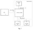
Fig. 1 schematically shows a flash memory system according to an exemplary embodiment of the invention; -
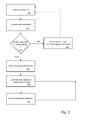
Fig. 2 is a flow chart of an automatic suspend on read procedure according to an embodiment of the invention; -
Fig. 3 is another flow chart showing a priority argument according to the method of invention; and -
Fig. 4 is another flow chart showing a suspend argument according to the method of the invention. - In
Fig. 1 , the arrangement according to the invention is shown schematically. Thenon-volatile memory device 1 comprises at least one NAND typeflash memory chip memory controller 2 which has a interface to anexternal host 4. Theexternal host device 4 may be represented by a terminal comprising a processor for executing program code stored in a storage medium. The host may need information stored on thememory device 1 to execute program code or to display the information on the host, such as an internal flash memory or a flash memory card in a mobile communication terminal. The host may be capable of controlling this memory access and to communicate data with the memory device. For this purpose, the host is connected to the memory controller or, alternatively, directly to the memory device if the host is responsible for all access controls and if the structure of the memory device does not require a separate controller. The host may for example be a desktop computer, a handheld computer, a mobile telephone, a digital camera or any other kind of computer/microcontroller based terminal which can use non-volatile memory as a storage medium. The non-volatile memory device may be provided e.g. as a removable memory element (memory card) or as embedded mass storage arranged within the device. - A read/write
port 8 of thememory controller 2 is used for accessing the NAND memory chips to perform read and/or write operations on thememory chip 1 according to predefined specifications. The memory chips include read-write data (i.e. for data storage) as well as read-only data (e.g. program code) on several partitions. The read-write data may be located in several chips or in several blocks of at least one memory chip. - By providing a set of commands (single state machine) and/or registers (multiple state machines), the memory controller is able to allow read access to one first memory unit of the memory device while writing/erasing a second memory unit of the device. The memory units may correspond e.g. to separate NAND chips or to separate blocks of at least one memory chip. In case of NAND chips which are not capable of internal read-while-write operations or suspend operations, at least two NAND chips should be provided to apply the method of the invention.
- As shown in
Fig. 1 , the memory controller has a read-writeport 8 for read and write/erase access to NAND memory chips or to at least afirst memory unit write port 10 is implemented as a "virtual" port by means of the above mentioned command set and/or registers. This port is assigned for fast read access operations to read-only data on asecond memory unit 16 in the example ofFig. 1 . The host may communicate with thememory controller 2 via ahost interface 6, such that control of the read and write operations may optionally be performed by thehost 4. Data to be written onto the memory or to be read from the memory is also transferred via the host interface. - Another exemplary embodiment employs NAND type flash memory chips with additional functionality, which are expected to be developed within near future. The additional capabilities may include actual read-while-write access on NAND chips or suspend capabilities as known from other types of flash memory. Those added features provide that only one NAND chip is necessary to implement the idea of the invention, although multiple chips may be used just as in the case of a NAND architecture as described above.
- When simultaneous read/write operations are supported by a NAND chip, the memory card controller may issue commands to different memory blocks of the same NAND chip. In this way, a write/erase operation may be performed on a first memory block of a chip, while at the same time one or more read operations are performed on further memory blocks. Those may be located on the same NAND chip as the first memory block or on a different NAND chip. The memory card controller prevents overlapping of memory access (i.e. prevents more than one request being directed to a single memory bank).
- To prevent such overlapping, the controller should be aware of ongoing operations anywhere on the memory device. This may for example be ensured by a busy signal or by some kind of flag that indicates that access to the memory device is requested or in process. When an ongoing operation is detected or several requests are received by the controller, it will issue the commands in such a way that it is ensured that only one command at a time is directed to one memory unit, as described above.
- In a further exemplary embodiment of the invention, NAND chips with suspend capability are used to decrease read latencies. There, a write/erase operation is suspended to be able to execute a read operation with higher priority. The read process should be completed before resuming the interrupted write or erase operation. NAND memory devices with suspend times of 500 □ s are available and may be sufficient for real time read/write applications.
- For this purpose, several ways of implementing a new read command are feasible. One alternative is to define the set of commands in a way that any read command automatically has higher priority than erase/write commands. Then, use of a read command will trigger suspension of any ongoing operations on the memory chip. A possible implementation of such a automatic suspend on read procedure is shown in
Fig. 2 . - To reserve the possibility to decide on suspensions as the case arises, the host may include a priority argument in the read command frame that is detectable by the memory controller, such that not all read operations would necessarily trigger suspension. An example embodiment for this is shown in
Fig. 3 . The memory controller waits to receive new commands from the host instep 301. When a read command is received (step 302), the priority argument which is enclosed in this command is checked by the memory controller (303). The priority argument may e.g. be implemented in such a way that certain conditions need to be fulfilled to trigger a suspension, or several priority classes might be defined that allow the memory controller to determine whether a read command has higher priority than an active write/erase operation. The prior initiation of this write/erase operation is not shown inFig. 3 . In the following it is assumed by way of example that the priority of the read command is given as a bit value or numerical value, and a preset priority threshold is defined for the memory controller. If the priority argument of the received read command exceeds the preset priority threshold, any ongoing write/erase operation or alternatively any operation, including a read operation, is suspended (step 305). If however the priority argument shows lower priority of the received read command, the ongoing operation is continued without interruption and the read command is not executed (step 304). This may be signalled to the host in a response. Optionally, the read command may be stored in a suitable manner by the memory controller and executed once the write/erase operation is completed. - After suspension of the write/erase operation, the memory controller performs the read operation and transfers the data requested by the read command to the host as shown in
step 306. Following this, the write/erase operation may be resumed automatically by the memory controller (step 307). As can be seen fromstep 306, after the data transfer back to the host, the memory controller may already wait for new commands from the host. In this way a single write/erase operation or e.g. a sequential write may be suspended several times by read operations with corresponding priority arguments. Although the priority arguments are issued or included into the commands by the host, the memory controller is controlling the actual process. - In a similar way, a suspend argument may be added to a read command and thus trigger suspension of any other operation, as in the example of
Fig. 4 . When a read command is received by the memory controller instep 402, the memory controller would determine whether the read command includes a suspend argument or not, e.g. by checking a flag, instep 403. If a suspend argument is detected within the command, suspension of ongoing write operations and a subsequent read operation are performed as described for the case of a priority argument fromstep 305 onward. A read command without a suspend argument thus corresponds to a read command with lower priority ofFig. 3 and is only executed if no write/erase operation is in process on the memory unit. - Also, a separate suspend command may be issued that triggers suspension of ongoing operations, and subsequently any desired access command such as a read command may be processed on the memory chip in a conventional manner.
- Yet another possibility is to suspend any ongoing data transfer from and to the flash memory device, and to immediately issue a fast read command. This suspension of data transfer may be triggered in a way similar to the suspension of ongoing access operations, i.e. by a read command with or without priority argument or by a separate suspend command.
- The above command schemes or register extensions may be implemented on a state machine level so that suspension of write/erase operations or simultaneous read-while-write triggering enables a parallel state machine in addition to the existing access. This additional access may be regarded as a virtual port.
In all given examples, control of the memory access may alternatively be exercised by the host device instead of the memory controller. Memory chip access may be address controlled or non-address controlled, e.g. implemented via Chip Select signals. - The method of the invention might at first sight lead to increased cost of a system's flash memory due to additional logic needed and more expensive memory chips in general to support the idea of the invention. However, since in return typically less RAM will be required in a system, total memory cost in a system applying the method of the invention will be significantly reduced while at the same time further benefits as described for read latency are obtained.
- Thus, a method is given to implement NAND flash memory devices with low read latencies, such that memory cards and/or embedded memory with large storage capacities and fast access times are facilitated. While the invention has been explained with regard to particular embodiments, memory types and specific command schemes, a person skilled in the art will recognise that those are to be understood by way of example only and are in no way intended to limit the scope of the invention given by the description and the appended claims and any combination thereof. The specification and drawings are, accordingly, also to be regarded in an illustrative rather than a restrictive sense.
Claims (17)
- A method for controlling access operations in a non-volatile memory device, the non-volatile memory device comprising a memory controller and at least one NAND type memory chip, wherein said NAND type memory chip has suspend capability, the method comprising
suspending at least one write and/or erase operation on a first memory unit via a set of commands by said memory controller; and subsequently
initiating a read operation on a second memory unit via a set of commands by said memory controller. - The method of claim 1, wherein said set of commands includes a read command for initiating said read operation.
- The method of claim 2, wherein said read command automatically triggers suspension of any ongoing write/erase operation or any data transfer to and from said non-volatile memory device.
- The method of claim 2, wherein said read command includes a priority argument, the method further comprising
deciding if an ongoing write/erase operation is to be suspended, on the basis of said priority argument; or
deciding if an ongoing data transfer to and/or from is to be suspended, on the basis of said priority argument. - The method of claim 2, wherein said read command includes a suspend argument, and
wherein said suspending of said at least one write/erase operation is performed responsive to said suspend argument. - The method of claim 2, further comprising
issuing, prior to said read command, a suspend command for triggering suspension of any ongoing read/write operation or of any data transfer to and from said non-volatile memory device. - A computer program product comprising program code means stored on a computer readable medium for carrying out the operations of one of the previous method claims 1 to 6, when executed on a computer or processor.
- A non-volatile memory device, comprising a memory controller and at least one non-volatile memory chip, wherein first and second memory units are provided, wherein said memory controller is configured to initiate a write and/or erase operation on said first memory unit and is further configured to initiate a read operation on said second memory unit via a set of commands;
wherein said memory controller is adapted to carry out said read and said write and/or erase operations simultaneously;
wherein said memory controller is further configured to suspend access operations to a memory unit. - The memory device of claim 8, wherein said memory controller is further configured to detect an additional priority argument or suspend argument in said set of commands.
- The memory device of claim 8, wherein said memory controller is further configured to receive a separate suspend command for triggering suspension of any ongoing read/write operation or any data transfer to and from said non-volatile memory device.
- The memory device of claim 9 or 10, wherein said memory controller is configured to suspend said write and/or erase operation on said first memory unit in response to said suspend argument or said suspend command; and
to subsequently initiate said read operation on said second memory unit. - The memory device of any of claims 8 to 11, wherein said first and second memory units correspond to separate blocks of at least one NAND type flash memory chip.
- The memory device of any of claims 8 to 11, comprising at least two NAND type flash memory chips, wherein said first and second memory units correspond to a first and a second NAND type flash memory chip.
- A host device comprising
a data transfer unit configured to communicate data between said host device and a non-volatile memory device, a command unit configured to issue control commands to said non-volatile memory device,
wherein said host device is capable of controlling said non-volatile memory device such that a second access operation is initiated on said non-volatile memory device before a first ongoing access operation is completed. - A memory module comprising a memory controller and at least one non-volatile memory chip, wherein first and second memory units are provided,
wherein said memory controller is configured to initiate a write and/or erase operation on said first memory unit, and is further configured to initiate a read operation on said second memory unit via a set of commands;
wherein said memory controller is adapted to perform said read and said write and/or erase operations simultaneously. - A system comprising a memory module according to claim 15 and a host device according to claim 14.
- A device, comprising
at least one non-volatile memory device, wherein first and second memory units are provided;
means for initiating a write and/or erase operation on a first memory unit of said non-volatile memory device;
means for initiating a read operation on a second memory unit of said non-volatile memory device;
means for controlling said read and write/erase operations to be performed simultaneously; and
means for suspending access operations to a memory unit.
Applications Claiming Priority (2)
| Application Number | Priority Date | Filing Date | Title |
|---|---|---|---|
| US11/390,969 US7562180B2 (en) | 2006-03-28 | 2006-03-28 | Method and device for reduced read latency of non-volatile memory |
| EP07705487A EP1999754A1 (en) | 2006-03-28 | 2007-01-30 | Method and device for reduced read latency of non-volatile memory |
Related Parent Applications (1)
| Application Number | Title | Priority Date | Filing Date |
|---|---|---|---|
| EP07705487.2 Division | 2007-01-30 |
Publications (1)
| Publication Number | Publication Date |
|---|---|
| EP2178090A1 true EP2178090A1 (en) | 2010-04-21 |
Family
ID=38540827
Family Applications (2)
| Application Number | Title | Priority Date | Filing Date |
|---|---|---|---|
| EP07705487A Withdrawn EP1999754A1 (en) | 2006-03-28 | 2007-01-30 | Method and device for reduced read latency of non-volatile memory |
| EP10152238A Withdrawn EP2178090A1 (en) | 2006-03-28 | 2007-01-30 | Method and device for reduced read latency of non-volatile memory |
Family Applications Before (1)
| Application Number | Title | Priority Date | Filing Date |
|---|---|---|---|
| EP07705487A Withdrawn EP1999754A1 (en) | 2006-03-28 | 2007-01-30 | Method and device for reduced read latency of non-volatile memory |
Country Status (8)
| Country | Link |
|---|---|
| US (1) | US7562180B2 (en) |
| EP (2) | EP1999754A1 (en) |
| JP (1) | JP2009528609A (en) |
| KR (1) | KR101078792B1 (en) |
| CN (1) | CN101410905A (en) |
| MY (2) | MY149576A (en) |
| TW (3) | TWI641952B (en) |
| WO (1) | WO2007110716A1 (en) |
Families Citing this family (96)
| Publication number | Priority date | Publication date | Assignee | Title |
|---|---|---|---|---|
| US7949806B2 (en) * | 2004-11-18 | 2011-05-24 | International Business Machines Corporation | Apparatus and method to provide an operation to an information storage device including protocol conversion and assigning priority levels to the operation |
| JP4250162B2 (en) * | 2005-09-16 | 2009-04-08 | シャープ株式会社 | Data processing device |
| US9734086B2 (en) | 2006-12-06 | 2017-08-15 | Sandisk Technologies Llc | Apparatus, system, and method for a device shared between multiple independent hosts |
| US8341300B1 (en) * | 2007-08-30 | 2012-12-25 | Virident Systems, Inc. | Systems for sustained read and write performance with non-volatile memory |
| US8200932B2 (en) | 2007-10-19 | 2012-06-12 | Virident Systems Inc. | Managing memory systems containing components with asymmetric characteristics |
| US7836226B2 (en) | 2007-12-06 | 2010-11-16 | Fusion-Io, Inc. | Apparatus, system, and method for coordinating storage requests in a multi-processor/multi-thread environment |
| US8209439B2 (en) * | 2008-08-25 | 2012-06-26 | Sandisk Il Ltd. | Managing multiple concurrent operations with various priority levels in a local storage device |
| US8250328B2 (en) * | 2009-03-24 | 2012-08-21 | Micron Technology, Inc. | Apparatus and method for buffered write commands in a memory |
| US20120179860A1 (en) * | 2009-06-10 | 2012-07-12 | Francesco Falanga | Suspension of memory operations for reduced read latency in memory arrays |
| US20110010512A1 (en) * | 2009-07-09 | 2011-01-13 | Mediatek Inc. | Method for controlling storage system having multiple non-volatile memory units and storage system using the same |
| US8850103B2 (en) * | 2009-08-28 | 2014-09-30 | Microsoft Corporation | Interruptible NAND flash memory |
| US9223514B2 (en) * | 2009-09-09 | 2015-12-29 | SanDisk Technologies, Inc. | Erase suspend/resume for memory |
| US9021158B2 (en) | 2009-09-09 | 2015-04-28 | SanDisk Technologies, Inc. | Program suspend/resume for memory |
| US8429436B2 (en) | 2009-09-09 | 2013-04-23 | Fusion-Io, Inc. | Apparatus, system, and method for power reduction in a storage device |
| US8972627B2 (en) * | 2009-09-09 | 2015-03-03 | Fusion-Io, Inc. | Apparatus, system, and method for managing operations for data storage media |
| KR101626084B1 (en) * | 2009-11-25 | 2016-06-01 | 삼성전자주식회사 | Multi-chip memory system and data transfer method thereof |
| JP2011150661A (en) * | 2010-01-25 | 2011-08-04 | Toshiba Corp | Portable electronic device and portable electronic device control method |
| US8429374B2 (en) * | 2010-01-28 | 2013-04-23 | Sony Corporation | System and method for read-while-write with NAND memory device |
| TWI486966B (en) * | 2010-02-04 | 2015-06-01 | Phison Electronics Corp | Flash memory storage device, controller thereof, and programming management method thereof |
| JP5495837B2 (en) * | 2010-02-17 | 2014-05-21 | アルパイン株式会社 | Navigation device using memory card |
| US20110252185A1 (en) * | 2010-04-08 | 2011-10-13 | Silicon Storage Technology, Inc. | Method Of Operating A NAND Memory Controller To Minimize Read Latency Time |
| CN102237136B (en) * | 2010-04-26 | 2014-05-14 | 旺宏电子股份有限公司 | Method for erasing storage subunits in a storage device |
| JP5378326B2 (en) * | 2010-08-17 | 2013-12-25 | 株式会社東芝 | Nonvolatile semiconductor memory device and control method thereof |
| US8984216B2 (en) | 2010-09-09 | 2015-03-17 | Fusion-Io, Llc | Apparatus, system, and method for managing lifetime of a storage device |
| US10817502B2 (en) | 2010-12-13 | 2020-10-27 | Sandisk Technologies Llc | Persistent memory management |
| US10817421B2 (en) | 2010-12-13 | 2020-10-27 | Sandisk Technologies Llc | Persistent data structures |
| US9218278B2 (en) | 2010-12-13 | 2015-12-22 | SanDisk Technologies, Inc. | Auto-commit memory |
| US9208071B2 (en) | 2010-12-13 | 2015-12-08 | SanDisk Technologies, Inc. | Apparatus, system, and method for accessing memory |
| US8819328B2 (en) * | 2010-12-30 | 2014-08-26 | Sandisk Technologies Inc. | Controller and method for performing background operations |
| US8364888B2 (en) * | 2011-02-03 | 2013-01-29 | Stec, Inc. | Erase-suspend system and method |
| CN102509556A (en) * | 2011-11-23 | 2012-06-20 | 常州金土木自动化研究所有限公司 | Passive remote single-wire-transmission read/write memory and working method thereof |
| US20130318285A1 (en) * | 2012-05-23 | 2013-11-28 | Violin Memory Inc | Flash memory controller |
| CN103809717B (en) * | 2012-11-09 | 2017-04-12 | 华为技术有限公司 | Resetting method and network device |
| KR20140093855A (en) | 2013-01-18 | 2014-07-29 | 삼성전자주식회사 | Memory system comprising nonvolatile memory device and control method thereof |
| US9779038B2 (en) * | 2013-01-31 | 2017-10-03 | Apple Inc. | Efficient suspend-resume operation in memory devices |
| US9792989B2 (en) * | 2013-02-07 | 2017-10-17 | Toshiba Memory Corporation | Memory system including nonvolatile memory |
| US9813080B1 (en) | 2013-03-05 | 2017-11-07 | Microsemi Solutions (U.S.), Inc. | Layer specific LDPC decoder |
| US10230396B1 (en) | 2013-03-05 | 2019-03-12 | Microsemi Solutions (Us), Inc. | Method and apparatus for layer-specific LDPC decoding |
| US9666244B2 (en) | 2014-03-01 | 2017-05-30 | Fusion-Io, Inc. | Dividing a storage procedure |
| KR20150116352A (en) | 2014-04-07 | 2015-10-15 | 삼성전자주식회사 | Memory control method and system |
| KR102254099B1 (en) | 2014-05-19 | 2021-05-20 | 삼성전자주식회사 | Method for processing memory swapping operation, and host device, storage device and data processing system adopting the same |
| US9812200B2 (en) * | 2014-07-08 | 2017-11-07 | Adesto Technologies Corporation | Concurrent read and write operations in a serial flash device |
| KR102203298B1 (en) | 2014-08-01 | 2021-01-15 | 삼성전자주식회사 | Nonvolatile memory device and driving method of the same |
| US9933950B2 (en) | 2015-01-16 | 2018-04-03 | Sandisk Technologies Llc | Storage operation interrupt |
| CN111857814B (en) * | 2015-05-18 | 2025-04-01 | 北京忆芯科技有限公司 | Memory controller that executes microinstructions |
| US10332613B1 (en) | 2015-05-18 | 2019-06-25 | Microsemi Solutions (Us), Inc. | Nonvolatile memory system with retention monitor |
| US9679658B2 (en) * | 2015-06-26 | 2017-06-13 | Intel Corporation | Method and apparatus for reducing read latency for a block erasable non-volatile memory |
| US9799405B1 (en) | 2015-07-29 | 2017-10-24 | Ip Gem Group, Llc | Nonvolatile memory system with read circuit for performing reads using threshold voltage shift read instruction |
| US10310770B2 (en) | 2015-11-05 | 2019-06-04 | Hitachi, Ltd. | Nonvolatile memory device, and storage apparatus having nonvolatile memory device |
| WO2017086925A1 (en) | 2015-11-17 | 2017-05-26 | Hewlett Packard Enterprise Development Lp | Iterative write sequence interrupt |
| US9886214B2 (en) | 2015-12-11 | 2018-02-06 | Ip Gem Group, Llc | Nonvolatile memory system with erase suspend circuit and method for erase suspend management |
| US9892794B2 (en) | 2016-01-04 | 2018-02-13 | Ip Gem Group, Llc | Method and apparatus with program suspend using test mode |
| US9899092B2 (en) | 2016-01-27 | 2018-02-20 | Ip Gem Group, Llc | Nonvolatile memory system with program step manager and method for program step management |
| US9812183B2 (en) | 2016-03-04 | 2017-11-07 | Adesto Technologies Corporation | Read latency reduction in a memory device |
| US10042587B1 (en) | 2016-03-15 | 2018-08-07 | Adesto Technologies Corporation | Automatic resumption of suspended write operation upon completion of higher priority write operation in a memory device |
| US10613763B2 (en) | 2016-04-21 | 2020-04-07 | Adesto Technologies Corporation | Memory device having multiple read buffers for read latency reduction |
| US10289596B2 (en) * | 2016-06-07 | 2019-05-14 | Macronix International Co., Ltd. | Memory and method for operating a memory with interruptible command sequence |
| US10055137B2 (en) | 2016-06-29 | 2018-08-21 | Intel Corporation | Method, system, and apparatus for nested suspend and resume in a solid state drive |
| US10157677B2 (en) | 2016-07-28 | 2018-12-18 | Ip Gem Group, Llc | Background reference positioning and local reference positioning using threshold voltage shift read |
| US10291263B2 (en) | 2016-07-28 | 2019-05-14 | Ip Gem Group, Llc | Auto-learning log likelihood ratio |
| US10236915B2 (en) | 2016-07-29 | 2019-03-19 | Microsemi Solutions (U.S.), Inc. | Variable T BCH encoding |
| US10558398B2 (en) * | 2016-07-29 | 2020-02-11 | Seagate Technology Llc | Reducing read latency |
| JP6753746B2 (en) * | 2016-09-15 | 2020-09-09 | キオクシア株式会社 | Semiconductor memory device |
| US11586565B2 (en) * | 2016-10-03 | 2023-02-21 | Samsung Electronics Co., Ltd. | Non-volatile storage system and data storage access protocol for non-volatile storage devices |
| KR102719399B1 (en) * | 2016-11-07 | 2024-10-21 | 에스케이하이닉스 주식회사 | Memory system and operating method thereof |
| CN108228075A (en) * | 2016-12-09 | 2018-06-29 | 北京忆恒创源科技有限公司 | The method and apparatus for accessing memory |
| CN106708441B (en) * | 2016-12-29 | 2019-06-21 | 至誉科技(武汉)有限公司 | A kind of operating method for reducing solid-state storage read latency |
| CN106775503A (en) * | 2017-02-23 | 2017-05-31 | 郑州云海信息技术有限公司 | A kind of method and device for performing operational order |
| KR102386811B1 (en) * | 2017-07-18 | 2022-04-15 | 에스케이하이닉스 주식회사 | Memory system and operating method thereof |
| CN107436737A (en) * | 2017-08-14 | 2017-12-05 | 郑州云海信息技术有限公司 | The method and system of suspend operation optimizations is handled in a kind of solid state hard disc |
| KR102447465B1 (en) * | 2017-09-08 | 2022-09-27 | 삼성전자주식회사 | A storage device that temporarily suspends internal operations to provide a short read response time for read requests from the host. |
| JP2019057147A (en) * | 2017-09-21 | 2019-04-11 | 東芝メモリ株式会社 | Memory system |
| CN108595118A (en) * | 2018-03-29 | 2018-09-28 | 深圳忆联信息系统有限公司 | A method of promoting solid state disk steady-state behaviour |
| US12393340B2 (en) | 2019-01-16 | 2025-08-19 | Pure Storage, Inc. | Latency reduction of flash-based devices using programming interrupts |
| US10509747B2 (en) * | 2018-05-17 | 2019-12-17 | Seagate Technology Llc | Memory access operation suspend/resume |
| US10475492B1 (en) | 2018-07-27 | 2019-11-12 | Macronix International Co., Ltd. | Circuit and method for read latency control |
| TWI684860B (en) * | 2018-10-15 | 2020-02-11 | 慧榮科技股份有限公司 | Method for performing read acceleration, and associated data storage device and controller thereof |
| WO2020095361A1 (en) | 2018-11-06 | 2020-05-14 | キオクシア株式会社 | Semiconductor storage device |
| JP2020098655A (en) | 2018-12-17 | 2020-06-25 | キオクシア株式会社 | Semiconductor memory device |
| KR102833711B1 (en) * | 2019-05-09 | 2025-07-14 | 에스케이하이닉스 주식회사 | Controller and memory system having the same |
| JP2021022414A (en) * | 2019-07-29 | 2021-02-18 | キオクシア株式会社 | Semiconductor storage device |
| KR20210031266A (en) * | 2019-09-11 | 2021-03-19 | 삼성전자주식회사 | Interface circuit, memory device, storage device and operation method of the memory device |
| US11237731B2 (en) * | 2019-10-24 | 2022-02-01 | Micron Technology, Inc. | Quality of service for memory devices using suspend and resume of program and erase operations |
| US11681352B2 (en) | 2019-11-26 | 2023-06-20 | Adesto Technologies Corporation | Standby current reduction in memory devices |
| CN111261206B (en) * | 2020-01-17 | 2022-03-08 | 苏州浪潮智能科技有限公司 | Read-write method and device, electronic equipment and readable storage medium |
| JP7337006B2 (en) * | 2020-03-03 | 2023-09-01 | キオクシア株式会社 | Memory system and control method |
| CN111739569B (en) * | 2020-06-19 | 2022-04-26 | 西安微电子技术研究所 | SDRAM (synchronous dynamic random access memory) control system and control method for reading and writing simultaneously |
| KR102851372B1 (en) * | 2020-07-28 | 2025-08-26 | 삼성전자주식회사 | Systems and methods for processing copy commands |
| US11366774B2 (en) | 2020-09-24 | 2022-06-21 | Adesto Technologies Corporation | Memory latency reduction in XIP mode |
| KR20220082509A (en) * | 2020-12-10 | 2022-06-17 | 에스케이하이닉스 주식회사 | Storage device and operating method thereof |
| CN113129952B (en) * | 2021-05-14 | 2023-04-18 | 长江存储科技有限责任公司 | Nonvolatile memory and control method thereof |
| US11704258B2 (en) | 2021-08-11 | 2023-07-18 | Dialog Semiconductor US Inc. | Latency reduction in SPI flash memory devices |
| US12014084B2 (en) | 2022-02-10 | 2024-06-18 | Stmicroelectronics S.R.L. | Data memory access collision manager, device and method |
| KR20240111522A (en) * | 2023-01-10 | 2024-07-17 | 에스케이하이닉스 주식회사 | Storage Device with Improved Read-Ahead Performance and Operation Method Thereof |
| WO2024182999A1 (en) * | 2023-03-07 | 2024-09-12 | Yangtze Memory Technologies Co., Ltd. | Managing operations in memory systems |
| CN117406935B (en) * | 2023-12-13 | 2024-02-20 | 苏州萨沙迈半导体有限公司 | Data reading method and device and read-write controller |
Citations (9)
| Publication number | Priority date | Publication date | Assignee | Title |
|---|---|---|---|---|
| US5333300A (en) * | 1991-02-11 | 1994-07-26 | Intel Corporation | Timing circuitry and method for controlling automated programming and erasing of a non-volatile semiconductor memory |
| US5355464A (en) * | 1991-02-11 | 1994-10-11 | Intel Corporation | Circuitry and method for suspending the automated erasure of a non-volatile semiconductor memory |
| US5559988A (en) * | 1993-12-30 | 1996-09-24 | Intel Corporation | Method and circuitry for queuing snooping, prioritizing and suspending commands |
| US5822244A (en) * | 1997-09-24 | 1998-10-13 | Motorola, Inc. | Method and apparatus for suspending a program/erase operation in a flash memory |
| US6260103B1 (en) * | 1998-01-05 | 2001-07-10 | Intel Corporation | Read-while-write memory including fewer verify sense amplifiers than read sense amplifiers |
| WO2002010921A1 (en) * | 2000-07-31 | 2002-02-07 | M-Systems Flash Disk Pioneers Ltd. | System and method for enabling non-volatile memory to execute code while operating as a data storage/processing device |
| US20020188812A1 (en) * | 2001-06-12 | 2002-12-12 | Akila Sadhasivan | Implementing a dual partition flash with suspend/resume capabilities |
| EP1345236A1 (en) * | 2002-03-14 | 2003-09-17 | STMicroelectronics S.r.l. | A non-volatile memory device |
| US20050160218A1 (en) * | 2004-01-20 | 2005-07-21 | Sun-Teck See | Highly integrated mass storage device with an intelligent flash controller |
Family Cites Families (22)
| Publication number | Priority date | Publication date | Assignee | Title |
|---|---|---|---|---|
| US5245572A (en) * | 1991-07-30 | 1993-09-14 | Intel Corporation | Floating gate nonvolatile memory with reading while writing capability |
| US5509134A (en) * | 1993-06-30 | 1996-04-16 | Intel Corporation | Method and apparatus for execution of operations in a flash memory array |
| JP3464271B2 (en) * | 1994-04-12 | 2003-11-05 | 三菱電機株式会社 | Nonvolatile semiconductor memory device |
| KR100359414B1 (en) * | 1996-01-25 | 2003-01-24 | 동경 엘렉트론 디바이스 주식회사 | Data reading method and memory controlling apparatus |
| GB2317721B (en) * | 1996-09-30 | 2001-09-12 | Nokia Mobile Phones Ltd | Memory device |
| US5867430A (en) * | 1996-12-20 | 1999-02-02 | Advanced Micro Devices Inc | Bank architecture for a non-volatile memory enabling simultaneous reading and writing |
| US6088264A (en) | 1998-01-05 | 2000-07-11 | Intel Corporation | Flash memory partitioning for read-while-write operation |
| DE19815914B4 (en) * | 1998-04-09 | 2005-05-04 | Alstom | distributor |
| GB9903490D0 (en) * | 1999-02-17 | 1999-04-07 | Memory Corp Plc | Memory system |
| US6772273B1 (en) | 2000-06-29 | 2004-08-03 | Intel Corporation | Block-level read while write method and apparatus |
| JP3699890B2 (en) * | 2000-08-30 | 2005-09-28 | シャープ株式会社 | Nonvolatile semiconductor memory device |
| US6556480B2 (en) * | 2000-12-29 | 2003-04-29 | Stmicroelectronics S.R.L. | EEPROM circuit, in particular a microcontroller including read while write EEPROM for code and data storing |
| US6584034B1 (en) * | 2001-04-23 | 2003-06-24 | Aplus Flash Technology Inc. | Flash memory array structure suitable for multiple simultaneous operations |
| US20040049628A1 (en) * | 2002-09-10 | 2004-03-11 | Fong-Long Lin | Multi-tasking non-volatile memory subsystem |
| US6988163B2 (en) * | 2002-10-21 | 2006-01-17 | Microsoft Corporation | Executing binary images from non-linear storage systems |
| US7155562B2 (en) * | 2003-05-08 | 2006-12-26 | Micron Technology, Inc. | Method for reading while writing to a single partition flash memory |
| JP3956305B2 (en) * | 2003-06-27 | 2007-08-08 | シャープ株式会社 | Nonvolatile semiconductor memory device and data processing device |
| JP4404625B2 (en) * | 2003-12-25 | 2010-01-27 | パナソニック株式会社 | Information processing apparatus and ROM image generation apparatus for the apparatus |
| JP4566621B2 (en) * | 2004-05-14 | 2010-10-20 | 富士通セミコンダクター株式会社 | Semiconductor memory |
| TWI260019B (en) * | 2004-05-21 | 2006-08-11 | Fujitsu Ltd | Semiconductor memory device and memory system |
| JP4182928B2 (en) * | 2004-07-07 | 2008-11-19 | セイコーエプソン株式会社 | Information processing apparatus, memory management program, and memory management method |
| US20070180186A1 (en) * | 2006-01-27 | 2007-08-02 | Cornwell Michael J | Non-volatile memory management |
-
2006
- 2006-03-28 US US11/390,969 patent/US7562180B2/en active Active
-
2007
- 2007-01-30 MY MYPI20083518A patent/MY149576A/en unknown
- 2007-01-30 WO PCT/IB2007/000203 patent/WO2007110716A1/en not_active Ceased
- 2007-01-30 KR KR1020087023470A patent/KR101078792B1/en active Active
- 2007-01-30 EP EP07705487A patent/EP1999754A1/en not_active Withdrawn
- 2007-01-30 JP JP2008556864A patent/JP2009528609A/en active Pending
- 2007-01-30 EP EP10152238A patent/EP2178090A1/en not_active Withdrawn
- 2007-01-30 CN CNA2007800109163A patent/CN101410905A/en active Pending
- 2007-02-07 TW TW105100802A patent/TWI641952B/en active
- 2007-02-07 TW TW104109014A patent/TWI590064B/en active
- 2007-02-07 TW TW096104436A patent/TWI512476B/en active
-
2008
- 2008-09-10 MY MYPI2012005643A patent/MY158276A/en unknown
Patent Citations (9)
| Publication number | Priority date | Publication date | Assignee | Title |
|---|---|---|---|---|
| US5333300A (en) * | 1991-02-11 | 1994-07-26 | Intel Corporation | Timing circuitry and method for controlling automated programming and erasing of a non-volatile semiconductor memory |
| US5355464A (en) * | 1991-02-11 | 1994-10-11 | Intel Corporation | Circuitry and method for suspending the automated erasure of a non-volatile semiconductor memory |
| US5559988A (en) * | 1993-12-30 | 1996-09-24 | Intel Corporation | Method and circuitry for queuing snooping, prioritizing and suspending commands |
| US5822244A (en) * | 1997-09-24 | 1998-10-13 | Motorola, Inc. | Method and apparatus for suspending a program/erase operation in a flash memory |
| US6260103B1 (en) * | 1998-01-05 | 2001-07-10 | Intel Corporation | Read-while-write memory including fewer verify sense amplifiers than read sense amplifiers |
| WO2002010921A1 (en) * | 2000-07-31 | 2002-02-07 | M-Systems Flash Disk Pioneers Ltd. | System and method for enabling non-volatile memory to execute code while operating as a data storage/processing device |
| US20020188812A1 (en) * | 2001-06-12 | 2002-12-12 | Akila Sadhasivan | Implementing a dual partition flash with suspend/resume capabilities |
| EP1345236A1 (en) * | 2002-03-14 | 2003-09-17 | STMicroelectronics S.r.l. | A non-volatile memory device |
| US20050160218A1 (en) * | 2004-01-20 | 2005-07-21 | Sun-Teck See | Highly integrated mass storage device with an intelligent flash controller |
Also Published As
| Publication number | Publication date |
|---|---|
| US7562180B2 (en) | 2009-07-14 |
| TWI590064B (en) | 2017-07-01 |
| TWI512476B (en) | 2015-12-11 |
| KR101078792B1 (en) | 2011-11-02 |
| KR20080099336A (en) | 2008-11-12 |
| US20070239926A1 (en) | 2007-10-11 |
| MY158276A (en) | 2016-09-30 |
| TW201614510A (en) | 2016-04-16 |
| MY149576A (en) | 2013-09-13 |
| TW200739354A (en) | 2007-10-16 |
| CN101410905A (en) | 2009-04-15 |
| WO2007110716A1 (en) | 2007-10-04 |
| TWI641952B (en) | 2018-11-21 |
| JP2009528609A (en) | 2009-08-06 |
| EP1999754A1 (en) | 2008-12-10 |
| TW201525701A (en) | 2015-07-01 |
Similar Documents
| Publication | Publication Date | Title |
|---|---|---|
| US7562180B2 (en) | Method and device for reduced read latency of non-volatile memory | |
| KR102688570B1 (en) | Memory System and Operation Method thereof | |
| US8429374B2 (en) | System and method for read-while-write with NAND memory device | |
| KR100843546B1 (en) | Multi-chip Package Flash Memory Device and Its Status Signal Reading Method | |
| US7215580B2 (en) | Non-volatile memory control | |
| KR102526608B1 (en) | Electronic device and operating method thereof | |
| KR101409095B1 (en) | Memory device and controlling method of the same | |
| JP5275623B2 (en) | Memory controller and memory system | |
| US10585822B2 (en) | Operation method of host system including storage device and operation method of storage device controller | |
| JPH1131102A (en) | Data storage system and access control method applied to the system | |
| KR20060027619A (en) | Multi-chip system and its bootcode fetch method | |
| KR102766448B1 (en) | Controller, operating method thereof and storage device including the same | |
| KR102696398B1 (en) | Memory controller, storage device including the same and operating method thereof | |
| KR20190120573A (en) | Memory system, data processing system and operating method of the memory system | |
| US10528285B2 (en) | Data storage device and method for operating non-volatile memory | |
| US10528360B2 (en) | Storage device, information processing system, method of activating storage device and program | |
| US11550740B2 (en) | Data storage device with an exclusive channel for flag checking of read data, and non-volatile memory control method | |
| KR20190090629A (en) | Memory system and operating method thereof | |
| US12596507B2 (en) | Apparatus and method for controlling nonvolatile memory | |
| US20260016960A1 (en) | I/O Prioritization During Model Load | |
| US10387076B2 (en) | Methods for scheduling data-programming tasks and apparatuses using the same |
Legal Events
| Date | Code | Title | Description |
|---|---|---|---|
| PUAI | Public reference made under article 153(3) epc to a published international application that has entered the european phase |
Free format text: ORIGINAL CODE: 0009012 |
|
| 17P | Request for examination filed |
Effective date: 20100201 |
|
| AC | Divisional application: reference to earlier application |
Ref document number: 1999754 Country of ref document: EP Kind code of ref document: P |
|
| AK | Designated contracting states |
Kind code of ref document: A1 Designated state(s): AT BE BG CH CY CZ DE DK EE ES FI FR GB GR HU IE IS IT LI LT LU LV MC NL PL PT RO SE SI SK TR |
|
| AX | Request for extension of the european patent |
Extension state: AL BA HR MK RS |
|
| 17Q | First examination report despatched |
Effective date: 20100609 |
|
| RAP1 | Party data changed (applicant data changed or rights of an application transferred) |
Owner name: MEMORY TECHNOLOGIES LLC |
|
| STAA | Information on the status of an ep patent application or granted ep patent |
Free format text: STATUS: THE APPLICATION IS DEEMED TO BE WITHDRAWN |
|
| 18D | Application deemed to be withdrawn |
Effective date: 20170801 |