EP2175497A2 - Lichtdiode - Google Patents
Lichtdiode Download PDFInfo
- Publication number
- EP2175497A2 EP2175497A2 EP09162426A EP09162426A EP2175497A2 EP 2175497 A2 EP2175497 A2 EP 2175497A2 EP 09162426 A EP09162426 A EP 09162426A EP 09162426 A EP09162426 A EP 09162426A EP 2175497 A2 EP2175497 A2 EP 2175497A2
- Authority
- EP
- European Patent Office
- Prior art keywords
- layer
- photodiode according
- diode
- photodiode
- thickness
- Prior art date
- Legal status (The legal status is an assumption and is not a legal conclusion. Google has not performed a legal analysis and makes no representation as to the accuracy of the status listed.)
- Granted
Links
Images


Classifications
-
- H—ELECTRICITY
- H10—SEMICONDUCTOR DEVICES; ELECTRIC SOLID-STATE DEVICES NOT OTHERWISE PROVIDED FOR
- H10F—INORGANIC SEMICONDUCTOR DEVICES SENSITIVE TO INFRARED RADIATION, LIGHT, ELECTROMAGNETIC RADIATION OF SHORTER WAVELENGTH OR CORPUSCULAR RADIATION
- H10F30/00—Individual radiation-sensitive semiconductor devices in which radiation controls the flow of current through the devices, e.g. photodetectors
- H10F30/20—Individual radiation-sensitive semiconductor devices in which radiation controls the flow of current through the devices, e.g. photodetectors the devices having potential barriers, e.g. phototransistors
- H10F30/21—Individual radiation-sensitive semiconductor devices in which radiation controls the flow of current through the devices, e.g. photodetectors the devices having potential barriers, e.g. phototransistors the devices being sensitive to infrared, visible or ultraviolet radiation
- H10F30/22—Individual radiation-sensitive semiconductor devices in which radiation controls the flow of current through the devices, e.g. photodetectors the devices having potential barriers, e.g. phototransistors the devices being sensitive to infrared, visible or ultraviolet radiation the devices having only one potential barrier, e.g. photodiodes
- H10F30/225—Individual radiation-sensitive semiconductor devices in which radiation controls the flow of current through the devices, e.g. photodetectors the devices having potential barriers, e.g. phototransistors the devices being sensitive to infrared, visible or ultraviolet radiation the devices having only one potential barrier, e.g. photodiodes the potential barrier working in avalanche mode, e.g. avalanche photodiodes
-
- H—ELECTRICITY
- H10—SEMICONDUCTOR DEVICES; ELECTRIC SOLID-STATE DEVICES NOT OTHERWISE PROVIDED FOR
- H10F—INORGANIC SEMICONDUCTOR DEVICES SENSITIVE TO INFRARED RADIATION, LIGHT, ELECTROMAGNETIC RADIATION OF SHORTER WAVELENGTH OR CORPUSCULAR RADIATION
- H10F30/00—Individual radiation-sensitive semiconductor devices in which radiation controls the flow of current through the devices, e.g. photodetectors
- H10F30/20—Individual radiation-sensitive semiconductor devices in which radiation controls the flow of current through the devices, e.g. photodetectors the devices having potential barriers, e.g. phototransistors
- H10F30/21—Individual radiation-sensitive semiconductor devices in which radiation controls the flow of current through the devices, e.g. photodetectors the devices having potential barriers, e.g. phototransistors the devices being sensitive to infrared, visible or ultraviolet radiation
- H10F30/22—Individual radiation-sensitive semiconductor devices in which radiation controls the flow of current through the devices, e.g. photodetectors the devices having potential barriers, e.g. phototransistors the devices being sensitive to infrared, visible or ultraviolet radiation the devices having only one potential barrier, e.g. photodiodes
- H10F30/225—Individual radiation-sensitive semiconductor devices in which radiation controls the flow of current through the devices, e.g. photodetectors the devices having potential barriers, e.g. phototransistors the devices being sensitive to infrared, visible or ultraviolet radiation the devices having only one potential barrier, e.g. photodiodes the potential barrier working in avalanche mode, e.g. avalanche photodiodes
- H10F30/2255—Individual radiation-sensitive semiconductor devices in which radiation controls the flow of current through the devices, e.g. photodetectors the devices having potential barriers, e.g. phototransistors the devices being sensitive to infrared, visible or ultraviolet radiation the devices having only one potential barrier, e.g. photodiodes the potential barrier working in avalanche mode, e.g. avalanche photodiodes in which the active layers form heterostructures, e.g. SAM structures
-
- H—ELECTRICITY
- H10—SEMICONDUCTOR DEVICES; ELECTRIC SOLID-STATE DEVICES NOT OTHERWISE PROVIDED FOR
- H10F—INORGANIC SEMICONDUCTOR DEVICES SENSITIVE TO INFRARED RADIATION, LIGHT, ELECTROMAGNETIC RADIATION OF SHORTER WAVELENGTH OR CORPUSCULAR RADIATION
- H10F30/00—Individual radiation-sensitive semiconductor devices in which radiation controls the flow of current through the devices, e.g. photodetectors
- H10F30/20—Individual radiation-sensitive semiconductor devices in which radiation controls the flow of current through the devices, e.g. photodetectors the devices having potential barriers, e.g. phototransistors
- H10F30/21—Individual radiation-sensitive semiconductor devices in which radiation controls the flow of current through the devices, e.g. photodetectors the devices having potential barriers, e.g. phototransistors the devices being sensitive to infrared, visible or ultraviolet radiation
- H10F30/22—Individual radiation-sensitive semiconductor devices in which radiation controls the flow of current through the devices, e.g. photodetectors the devices having potential barriers, e.g. phototransistors the devices being sensitive to infrared, visible or ultraviolet radiation the devices having only one potential barrier, e.g. photodiodes
- H10F30/227—Individual radiation-sensitive semiconductor devices in which radiation controls the flow of current through the devices, e.g. photodetectors the devices having potential barriers, e.g. phototransistors the devices being sensitive to infrared, visible or ultraviolet radiation the devices having only one potential barrier, e.g. photodiodes the potential barrier being a Schottky barrier
-
- H—ELECTRICITY
- H10—SEMICONDUCTOR DEVICES; ELECTRIC SOLID-STATE DEVICES NOT OTHERWISE PROVIDED FOR
- H10F—INORGANIC SEMICONDUCTOR DEVICES SENSITIVE TO INFRARED RADIATION, LIGHT, ELECTROMAGNETIC RADIATION OF SHORTER WAVELENGTH OR CORPUSCULAR RADIATION
- H10F39/00—Integrated devices, or assemblies of multiple devices, comprising at least one element covered by group H10F30/00, e.g. radiation detectors comprising photodiode arrays
- H10F39/10—Integrated devices
- H10F39/103—Integrated devices the at least one element covered by H10F30/00 having potential barriers, e.g. integrated devices comprising photodiodes or phototransistors
-
- H—ELECTRICITY
- H10—SEMICONDUCTOR DEVICES; ELECTRIC SOLID-STATE DEVICES NOT OTHERWISE PROVIDED FOR
- H10F—INORGANIC SEMICONDUCTOR DEVICES SENSITIVE TO INFRARED RADIATION, LIGHT, ELECTROMAGNETIC RADIATION OF SHORTER WAVELENGTH OR CORPUSCULAR RADIATION
- H10F77/00—Constructional details of devices covered by this subclass
- H10F77/10—Semiconductor bodies
- H10F77/12—Active materials
- H10F77/122—Active materials comprising only Group IV materials
- H10F77/1226—Active materials comprising only Group IV materials comprising multiple Group IV elements, e.g. SiC
-
- H—ELECTRICITY
- H10—SEMICONDUCTOR DEVICES; ELECTRIC SOLID-STATE DEVICES NOT OTHERWISE PROVIDED FOR
- H10F—INORGANIC SEMICONDUCTOR DEVICES SENSITIVE TO INFRARED RADIATION, LIGHT, ELECTROMAGNETIC RADIATION OF SHORTER WAVELENGTH OR CORPUSCULAR RADIATION
- H10F77/00—Constructional details of devices covered by this subclass
- H10F77/10—Semiconductor bodies
- H10F77/12—Active materials
- H10F77/124—Active materials comprising only Group III-V materials, e.g. GaAs
- H10F77/1248—Active materials comprising only Group III-V materials, e.g. GaAs having three or more elements, e.g. GaAlAs, InGaAs or InGaAsP
- H10F77/12485—Active materials comprising only Group III-V materials, e.g. GaAs having three or more elements, e.g. GaAlAs, InGaAs or InGaAsP comprising nitride compounds, e.g. InGaN
-
- H—ELECTRICITY
- H10—SEMICONDUCTOR DEVICES; ELECTRIC SOLID-STATE DEVICES NOT OTHERWISE PROVIDED FOR
- H10F—INORGANIC SEMICONDUCTOR DEVICES SENSITIVE TO INFRARED RADIATION, LIGHT, ELECTROMAGNETIC RADIATION OF SHORTER WAVELENGTH OR CORPUSCULAR RADIATION
- H10F77/00—Constructional details of devices covered by this subclass
- H10F77/10—Semiconductor bodies
- H10F77/14—Shape of semiconductor bodies; Shapes, relative sizes or dispositions of semiconductor regions within semiconductor bodies
- H10F77/147—Shapes of bodies
-
- H—ELECTRICITY
- H10—SEMICONDUCTOR DEVICES; ELECTRIC SOLID-STATE DEVICES NOT OTHERWISE PROVIDED FOR
- H10F—INORGANIC SEMICONDUCTOR DEVICES SENSITIVE TO INFRARED RADIATION, LIGHT, ELECTROMAGNETIC RADIATION OF SHORTER WAVELENGTH OR CORPUSCULAR RADIATION
- H10F77/00—Constructional details of devices covered by this subclass
- H10F77/20—Electrodes
- H10F77/206—Electrodes for devices having potential barriers
- H10F77/241—Electrodes for devices having potential barriers comprising ring electrodes
Definitions
- the present invention relates to an avalanche photodiode for detecting ultraviolet photons.
- Ultraviolet radiation covers the region of the electromagnetic spectrum below the wavelength of visible light from 400 nm down to about 1 nm. This radiation is a highly ionizing radiation, which activates many chemical processes. A major natural UV source is the sun.
- the near-UV region (200-400 nm) is commonly divided into three sub-regions, in which the most common division is:
- UVA 99% of the UV radiation from the sun reaching the earth surface is UVA.
- a small amount of UVB reaches the surface.
- This is the primary agent responsible for sun burn on skin, but also has the beneficial effect of inducing the production of vitamin D in skin.
- the UVC region is of great interest for UV detection, since radiation of this wavelength is heavily absorbed by the ozone layer, and any UVC light encountered at the earth's surface almost always comes from a man-made source.
- the extremely low background level in this region permits the detection of very low levels of earth-generated radiation.
- UV-radiation is useful for a wide range of civil and military applications, such as chemical and biological analysis for identifying small concentrations of molecules, for instance for discovering the presence of bacteria in water.
- Other applications are flame detection, optical communications, process control and astronomical studies.
- a high sensitivity of such a photodiode making it possible to detect very low level radiation is required for several of these applications.
- This avalanche multiplication of the photo current results in an amplified signal of the diode, making this type of device ideal for detecting very low radiation levels.
- Such an avalanche photodiode may operate in two different modes: a linear mode, in which the reverse bias is close to, but not above the breakdown voltage of the diode, and a so-called Geiger mode, in which the reverse bias is increased above the breakdown voltage of the diode but still being close thereto.
- the present invention relates to such an avalanche photodiode as defined in the preamble of appended claim 1.
- the invention relates to an avalanche photodiode, in which the active region for avalanche multiplication of charge carriers is created in a said second layer of SiC or Al x Ga 1-x N, in which 0 ⁇ x ⁇ 0.5, which means that this active region will in the latter case in fact be of GaN with a possible substitution of gallium atoms by aluminium atoms.
- Gallium nitride has a direct band gap with a width that places the wavelength of maximum detection of the UV wavelength band at 365 nm (3.4 eV), which means that photons reaching a said active region have to have a wavelength being ⁇ 365 nm for having sufficient energy to create charge carriers in the form of electron-hole pairs in this region and by that being detected.
- GaN is well suited for use in a sensitive detector due to its low dark current (low noise) and high absorption coefficient. It is possible to adjust the width of the GaN bandgap by alloying it with aluminium, which permits tuning of the maximum detectable wavelength to lower wavelengths. Also, the direct bandgap promotes a sharp cut-off at the maximum detection wavelength that can be up to 5 orders of magnitude.
- Avalanche photodiodes for detecting ultraviolet photons of this type are disclosed in US 6 838 741 , US 5 596 186 and US 7 291 544 .
- a disadvantage of these ultraviolet detectors already known is that it may not be ensured that the generation of charge carriers for avalanche multiplication occurs in the bulk of the detector in said active region in order to avoid generation of charge carriers taking place at the edge of the device due to the electric field crowding normally occurring there, which would result in a very low efficiency and a non-uniform signal.
- the signal of such a photodiode may especially when used for detecting low level radiation have a high content not emanating from ultraviolet photons entering said active region of the device and by that not the reliability and stability required.
- the object of the present invention is to provide an avalanche photodiode according to the preamble of appended claim 1, which addresses the problem discussed above of a degraded stability, sensitivity and uniformity of the response signal in such photodiodes already known as a consequence of noise.
- This object is according to the invention obtained by providing such an avalanche photodiode with a fourth layer of for a) Al x Ga 1-x N and for b) SiC or Al x Ga 1-x N and doped according to a second conductivity type opposite to said first conductivity type arranged above said second layer laterally outside said surface with said second electrode arranged on top thereof, the thickness of said fourth layer and the doping concentration thereof are adapted to obtain an effective surface charge density of said fourth layer in a region laterally next to said surface obtaining an electric field strength substantially equal to a critical electric field strength of the diode at a pn-junction formed below said fourth layer laterally next to said surface upon application of a said voltage across said electrodes, and an edge termination extension of the diode is obtained as of said lateral border by a reduction of said effective surface charge density in the direction laterally away from said surface.
- said edge termination extension is obtained by a reduction of said effective surface charge density in said fourth layer in a plurality of steps separated by a lateral distance of 1-10 ⁇ m, with the minimum number of steps being 1. This results in an efficient removal of edge influences upon the signal of the photodiode.
- said effective surface charge density being a product of said fourth layer electrically active doping and thickness under said second electrode is minimum 1x10 13 cm -2 and most preferred approximately 1.3x10 13 cm -2 .
- said fourth layer has a thickness being stepwisely or gradually reduced in the lateral direction away from said surface lateral border to be zero at an end of said edge termination extension where the uppermost semiconductor layer of the diode is of said first conductivity type, so that the electric field will be accurately controlled to be zero at said end.
- the doping concentration of said fourth layer is 3x10 16 -10 19 cm -3 next to said surface and the thickness of said fourth layer under said second electrode is 5 ⁇ m - 0.015 ⁇ m and preferably 1-2 ⁇ 10 18 cm -3 and 0.15-0.075 ⁇ m, respectively.
- the critical electrical field of the semiconductor material Al x Ga 1-x N used here is in the order of 2x10 6 V/cm and for a certain breakdown voltage of the photodiode said fourth layer may be made thicker with a decreasing doping concentration of the fourth layer next to said surface, so that the thickness of this layer may be selected by selecting the doping concentration thereof.
- the thickness of said second layer is 0.05-0.5 ⁇ m.
- This thin lightly doped second layer means that the entire second layer will be depleted when the photodiode is reverse biased, so that the electric field strength therein will be constant and a well defined volume for avalanche multiplication will be formed therein.
- Another advantage of having such a thin second layer is that it may be totally depleted already at a low voltage, so that the photodiode will have a low breakdown voltage and by that operation voltage, well in the order of 10-20 V making it possible to use for instance conventional batteries for the operation of the diode substantially facilitating the handling of the photodiode and associated equipment.
- the photodiode comprises a fifth doped semiconductor layer of Al y Ga 1-y N on top of said second layer with y ⁇ x, in which this x is for said second layer.
- a fifth layer is particularly advantageous if y is larger than x, which means that shorter radiation wavelengths are needed for being absorbed by said fifth layer than by said second layer, so that wavelengths thereabove to be detected by the photodiode will not be absorbed by the fifth layer but reach the second layer.
- said fourth layer extends all the way over said second layer forming said third layer and a pn-junction to said second layer in the area to be exposed to the photons to be detected.
- said fourth layer is preferably of Al y Ga 1-y N with y ⁇ x, in which this x is for said second layer.
- a thin fifth layer is of course of less importance when y>x.
- said fifth layer is doped according to said second conductivity type for forming said third layer by forming a pn-junction to said second layer.
- This fifth layer may then be of the same material as said second layer, which however, as already mentioned, means that it will absorb photons of the same wavelengths as the second layer and has therefore to be very thin. Accordingly, it is preferred that the band gap of this fifth layer is greater than of said second layer.
- said fifth layer may be identical with the said fourth layer by arranging the said fourth layer over both said edge termination area and said active area of the diode.
- the photodiode comprises a highly doped semiconductor layer of for a) Al x Ga 1-x N and for b) Al x Ga 1-x N or SiC and doped according to said second conductivity type located directly under said second electrode for making a good ohmic contact thereto. This results in an efficient conducting of the charge carriers to this second electrode.
- said contact layer covers said fifth layer in the area to be exposed to the photons to be detected.
- said effective surface charge density which is a sum of a product of said fifth layer electrically active doping and thickness and product of corresponding doping and thickness of any other layer overlaying said fifth layer in the area to be exposed to the photons to be detected, is minimum 1x10 13 cm -2 .
- a metal layer of a thickness below 0.05 ⁇ m, preferably 0.02-0.005 ⁇ m, is arranged on top of said fifth layer in said surface and extends to said second electrode for conducting charge carriers thereto.
- a metal layer makes the conduction of charge carriers to the second electrode more efficient, but it has to be made very thin for being semi-transparent and not reflecting too much of the photons hitting the active surface of the photodiode.
- said third layer is formed by a metal layer forming a Schottky junction to a semiconductor layer therebelow, and said fifth layer will then be doped according to said first conductivity type and arranged directly under said third layer.
- a Schottky barrier so formed will be lower than the barrier of a pn-junction, which will result in higher leakage currents and a higher temperature dependence of the photodiode, so that it is in such a case advantageous to have a fifth layer with y being considerably higher than 0, such as 0.2-0.5 resulting in a higher Schottky barrier and lower leakage currents and a reduced temperature dependence than if y were 0, i.e. the material was GaN.
- Said Schottky metal layer has a thickness below 0.05 ⁇ m, preferably 0.02-0.005 ⁇ m and extends to said second electrode for conducting charge carriers thereto.
- said first conductivity type is n and said second conductivity type is p.
- the thickness of said first layer is at least 2 ⁇ m, preferably 2-10 ⁇ m.
- the doping concentration of said first layer is at least one order of magnitude higher than the doping concentration of said second layer. This means that the second layer may easily be depleted and the electric field will be stopped to fall to substantially zero by said first layer.
- the doping concentration of said first layer is 5x10 17 - 5x10 19 cm -3 and the doping concentration of said second layer is 1x10 16 - 2x10 17 cm -3 .
- a low doping concentration of the second layer in combination with the reduced thickness thereof will make it possible to reach the critical electric field for avalanche within the entire second layer at a low reverse voltage, such as 10 - 20 V.
- the doping concentration of said fifth layer is 10 17 -10 18 cm -3 .
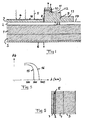
- Fig 1 very schematically illustrates the design of an avalanche photodiode for detecting ultraviolet photons according an embodiment of the invention, in which the relationship of the dimensions of the different layers are not drawn to scale, but the drawing is merely intended to explain the structure of the photodiode.
- the photodiode has a first semiconductor layer 1 highly doped according to a first conductivity type, in which said first conductivity type may be n or p, and it is here n.
- This layer has here a thickness of 1-10 ⁇ m and a doping concentration of 5x10 17 - 5x10 19 cm -3 . It is in the present case GaN, but it may just as well be Al x Ga 1-x N, with 0 ⁇ x ⁇ 0.5.
- a second semiconductor layer 2 of GaN is arranged on top of the first layer 1. This layer is also doped according to the first conductivity type, which here is n.
- This second layer has a thickness of about 0.1-0.5 ⁇ m and a doping concentration of 1x10 15 - 5x10 16 cm -3 .
- a third layer 3 is located on top of the second layer and configured to form a blocking junction to the second layer in a reverse biased state of the diode, and this third layer is here doped according to a second conductivity type, which here means p, for forming a pn-junction to the second layer.
- This third layer may be of the same material as the first and second layer, but it has preferably a higher content of Al, so that radiation of shorter wavelengths are required for creating charge carriers therein than in the second layer.
- the third layer shall be kept as thin as possible in order not to lower the optical gain of the photodiode due to absorption of the photons in this layer.
- the third layer has preferably a thickness of about 0.02-0.05 ⁇ m and a doping concentration of 2x10 18 - 1x10 19 cm -3 .
- the effective surface charge density N eff ⁇ 1.3 ⁇ 10 13 cm -2 .
- a surface 4 of the diode above said third layer is configured to be exposed to photons 5 to be detected.
- a first electrode 6 is arranged below the first layer 1, in the case of a conducting substrate S of for example SiC or GaN and is arranged in contact with said conducting substrate S or is arranged to the top of the first layer 1 in the case of an insulating substrate S of for example Al 2 O 3 (as in the embodiment shown in Fig 4 ), and a second electrode 7 is located above said third layer laterally to said surface 4 and next to an outer lateral border 8 defining said surface.
- the said fourth layer 9 may be arranged by first removing the said third layer 3 beyond the outer lateral border 8 through etching, second by growing the said fourth layer 9 on top of said second 2 and said third 3 layers and by third removing the said fourth layer 9 over the said third layer 3 and over the said surface 4 by etching.
- the thickness of said fourth layer 9 and the doping concentration thereof are adapted to obtain an effective surface charge density of said fourth layer in a region 11 laterally next to said surface 4 for, upon application of a voltage close to the breakdown voltage of the diode across said electrodes, obtaining an electric field strength substantially equal to a critical electric field strength of the diode at a pn-junction 22 formed below said fourth layer laterally next to said surface.
- this layer 9 rather low doped for not requiring etching of very small steps and thus having larger tolerances during fabrication of diodes.
- An edge termination extension of the diode is obtained as of said lateral border 8 by a reduction of said effective surface charge density in the direction laterally away from said surface 4, which in the present case is made by stepwisely reducing the thickness of the fourth layer in subsequent regions 12, 13 and 14 in which it is zero in the region 14, i.e. etched down to the upper first conductivity type layer 2.
- Such a reduction of the thickness may also be combined or replaced by a reduction of the doping concentration of the fourth layer 9 in the lateral direction.
- the preferred effective surface charge density in the case of two steps as in Fig 1 , is in the region 12 between 30% and 60% and in the region 13 between 15% and 40% of the effective surface charge density in the region 11.
- the steps in the fourth layer 9 are preferably separated by a lateral distance of 1-10 ⁇ m.
- the region 11 has preferably a substantially constant effective surface charge density over a certain lateral distance as of the border 8, such as at least 2 ⁇ m.
- the fourth layer 9 is preferably covered by an insulating passivation layer in the part not covered by second electrode 7, not shown.
- the arrangement of such a metal layer will reduce said lateral resistivity so as to improve the conduction of charge carriers to the second electrode, but it will at the same time cause a reflection of a part of the photons reaching the surface 4, so it has to be made very thin and of a metal being transparent to said photons. It is then preferred to also have the third layer highly doped for obtaining a low resistance for the free charge carriers created by avalanche multiplication to reach the second electrode 7.
- the diode has preferably a cellular layout which means that it is built by repetition of unit cells with different geometry.
- Each unit cell contains said surface 4 and the surrounding area corresponding to the region covered by the said electrode 7.
- the edge termination according to Fig 1 is added only to the unit cells at the periphery of the diode.
- the preferred unit cell geometry may be linear-parallel, square, circular or hexagonal with the said surface 4 in the form of rectangles, squares, circles or hexagons, respectively.
- Fig 2 illustrates an avalanche photodiode according to a second embodiment of the invention, which differs from the diode shown in Fig 1 by the fact that said third layer 3 is here included in a said fourth layer 9 which covers the entire area of the diode. This reduces the number of processing steps compared to the first embodiment, however, the embodiment requires etching of small steps in the case when said fourth layer 9 is made out of GaN.
- the thickness of said fourth layer 9 over said active area of the diode according to the second embodiment of the invention may be made smaller compared to the thickness of said fourth layer 9 under said contact electrode 7 through etching as shown in Fig 4 .
- Fig 3 illustrates an avalanche photodiode according to a third embodiment of the invention differing from the embodiment shown in Fig 2 by the fact that at least said first 1 and second 2 layers are made of SiC, here of n-type with doping concentrations of for example 5x10 15 cm -3 for both and a thickness of 1-3 ⁇ m for the first layer and approximately 0.1 ⁇ m for the second layer. Furthermore, a highly doped n-type layer 20 of SiC having a doping concentration of for example 1x10 18 cm -3 and a thickness of 0.1 ⁇ m is introduced between the first layer 1 and the second layer 2 while extending only under the active area of the device and preferably not further than to the first etched step 12 of the termination.
- This extra layer 20 has an effective surface charge density, i.e. a product of thickness and doping concentration, preferably being less than 1.3x10 13 cm -2 .
- the fourth layer 9 may here be of the same type as in the embodiment according to Fig 2 , but it may also be, and is preferably, of SiC having a doping concentration in the region of 10 18 cm -3 . It is pointed out that the doping type can be the opposite in all layers, so that instead of having holes collected and multiplied in the n-type layers 1, 20 and 2, respectively, electrons may be collected and multiplied when making these layers of p-type instead.
- Fig 4 illustrates an avalanche photodiode according to a fourth embodiment of the invention, which differs from the one according to Fig 1 by the fact that the thin metal layer 18 has been replaced by an extension of the highly doped semiconductor layer 10 located under the second electrode 7 for making a good ohmic contact thereto.
- the substrate S is here made of an insulating material, such as Al 2 O 3 , so that the first electrode 6 is located on top of the first layer 1.
- the embodiment shown in Fig 2 may of course also be modified in a similar way should a substrate S of insulating material be used in that embodiment.
- Fig 5 illustrates the absorption Ab versus the wavelength ⁇ of photons reaching the surface 4 of the avalanche photodiode according to Fig 1 .
- the third layer 3 is made of a material absorbing according to the line 15 and the second layer 2, in which the active region for avalanche multiplication is formed, is formed of GaN, it is ensured that, if the third layer 3 is thin enough, most of the radiation with wavelengths above 280 nm reaches said second layer, so that photons with wavelengths of 280-365 nm may be detected by this photodiode.
- Selecting a certain thickness of the third layer 3 may then result in a nearly completely prevention of photons with a wavelength shorter than 280 nm from reaching the second layer 2 and be detected through avalanche multiplication, so that it may be concluded that the creation of a signal means a presence of photons with wavelengths in the range of 280-365 nm.
- Fig 6 illustrates how it will be possible to completely deplete said second layer 2 at a low voltage applied across the electrodes of the device thanks to a low doping concentration and a low thickness of this layer.
- the electric field E will be nearly constant across this layer 2 and an active region of avalanche multiplication of charge carriers may be formed across the substantially entire thickness of this second layer 2.
- Fig 7 illustrates the reverse current I versus the voltage U applied across the electrodes of the diode according to Fig 1 , and a reverse bias with a voltage of approximately 18 V close to the breakdown voltage of the diode is selected for the operation of the diode.
- Fig 8 illustrates an avalanche photodiode according to a fifth embodiment of the invention, which differs from the diode shown in Fig 1 by the fact that said third layer is replaced by a layer 17 of a first conductivity type, here n, and the metal layer 18 is here configured to form a blocking junction to the layer 17 in the form of a Schottky junction 21 in a reverse biased state of the diode.
- the edge termination extension may have a different number of steps than that shown in Fig 1 , and this has only to be reduced in thickness to reach the layer 17 and not to the second layer 2 as in the case of pn-junction.
- Dopants suitable to be used for the semiconductor material of the photodiode of Al x Ga 1-x N according to the invention are Si as donor and Mg and Zn as acceptors.
- the metal may be arranged directly on top of the second layer, although it is preferred to have a further thin layer on top thereof, especially with a higher content of Al for not absorbing radiation above a cut-off wavelength thereof and for obtaining a higher Schottky barrier.
- the photodiode may have more layers than those shown in the Figures.
Landscapes
- Light Receiving Elements (AREA)
Applications Claiming Priority (1)
| Application Number | Priority Date | Filing Date | Title |
|---|---|---|---|
| SE0801780 | 2008-08-12 |
Publications (3)
| Publication Number | Publication Date |
|---|---|
| EP2175497A2 true EP2175497A2 (de) | 2010-04-14 |
| EP2175497A3 EP2175497A3 (de) | 2017-12-27 |
| EP2175497B1 EP2175497B1 (de) | 2019-11-20 |
Family
ID=41728233
Family Applications (1)
| Application Number | Title | Priority Date | Filing Date |
|---|---|---|---|
| EP09162426.2A Active EP2175497B1 (de) | 2008-08-12 | 2009-06-10 | Lawinen-fotodiode zur detektion von photonen im ultravioletten bereich |
Country Status (1)
| Country | Link |
|---|---|
| EP (1) | EP2175497B1 (de) |
Cited By (5)
| Publication number | Priority date | Publication date | Assignee | Title |
|---|---|---|---|---|
| US8269222B2 (en) | 2010-05-25 | 2012-09-18 | The United States Of America As Represented By The Secretary Of The Army | Semiconductor photodetector with transparent interface charge control layer and method thereof |
| US8269223B2 (en) | 2010-05-27 | 2012-09-18 | The United States Of America As Represented By The Secretary Of The Army | Polarization enhanced avalanche photodetector and method thereof |
| CN103227231A (zh) * | 2013-04-19 | 2013-07-31 | 中国科学院半导体研究所 | 一种平面型雪崩光电探测器 |
| US9379271B2 (en) | 2013-05-24 | 2016-06-28 | The United States Of America As Represented By The Secretary Of The Army | Variable range photodetector and method thereof |
| US9893227B2 (en) | 2013-05-24 | 2018-02-13 | The United States Of America As Represented By The Secretary Of The Army | Enhanced deep ultraviolet photodetector and method thereof |
Families Citing this family (1)
| Publication number | Priority date | Publication date | Assignee | Title |
|---|---|---|---|---|
| US10957807B2 (en) * | 2017-04-19 | 2021-03-23 | The Board Of Trustees Of The University Of Alabama | PLZT thin film capacitors apparatus with enhanced photocurrent and power conversion efficiency and method thereof |
Citations (3)
| Publication number | Priority date | Publication date | Assignee | Title |
|---|---|---|---|---|
| US5596186A (en) | 1993-12-08 | 1997-01-21 | Nikon Corporation | High sensitivity silicon avalanche photodiode |
| US6838741B2 (en) | 2002-12-10 | 2005-01-04 | General Electtric Company | Avalanche photodiode for use in harsh environments |
| US7291544B2 (en) | 2001-04-20 | 2007-11-06 | General Electric Company | Homoepitaxial gallium nitride based photodetector and method of producing |
Family Cites Families (5)
| Publication number | Priority date | Publication date | Assignee | Title |
|---|---|---|---|---|
| CA1280196C (en) * | 1987-07-17 | 1991-02-12 | Paul Perry Webb | Avanlanche photodiode |
| US5967795A (en) * | 1995-08-30 | 1999-10-19 | Asea Brown Boveri Ab | SiC semiconductor device comprising a pn junction with a voltage absorbing edge |
| US7033950B2 (en) * | 2001-12-19 | 2006-04-25 | Auburn University | Graded junction termination extensions for electronic devices |
| JP3873798B2 (ja) * | 2002-04-11 | 2007-01-24 | 富士電機デバイステクノロジー株式会社 | 炭化けい素半導体素子およびその製造方法 |
| CN201000897Y (zh) * | 2006-12-20 | 2008-01-02 | 厦门大学 | 4H-SiC雪崩光电探测器 |
-
2009
- 2009-06-10 EP EP09162426.2A patent/EP2175497B1/de active Active
Patent Citations (3)
| Publication number | Priority date | Publication date | Assignee | Title |
|---|---|---|---|---|
| US5596186A (en) | 1993-12-08 | 1997-01-21 | Nikon Corporation | High sensitivity silicon avalanche photodiode |
| US7291544B2 (en) | 2001-04-20 | 2007-11-06 | General Electric Company | Homoepitaxial gallium nitride based photodetector and method of producing |
| US6838741B2 (en) | 2002-12-10 | 2005-01-04 | General Electtric Company | Avalanche photodiode for use in harsh environments |
Cited By (5)
| Publication number | Priority date | Publication date | Assignee | Title |
|---|---|---|---|---|
| US8269222B2 (en) | 2010-05-25 | 2012-09-18 | The United States Of America As Represented By The Secretary Of The Army | Semiconductor photodetector with transparent interface charge control layer and method thereof |
| US8269223B2 (en) | 2010-05-27 | 2012-09-18 | The United States Of America As Represented By The Secretary Of The Army | Polarization enhanced avalanche photodetector and method thereof |
| CN103227231A (zh) * | 2013-04-19 | 2013-07-31 | 中国科学院半导体研究所 | 一种平面型雪崩光电探测器 |
| US9379271B2 (en) | 2013-05-24 | 2016-06-28 | The United States Of America As Represented By The Secretary Of The Army | Variable range photodetector and method thereof |
| US9893227B2 (en) | 2013-05-24 | 2018-02-13 | The United States Of America As Represented By The Secretary Of The Army | Enhanced deep ultraviolet photodetector and method thereof |
Also Published As
| Publication number | Publication date |
|---|---|
| EP2175497B1 (de) | 2019-11-20 |
| EP2175497A3 (de) | 2017-12-27 |
Similar Documents
| Publication | Publication Date | Title |
|---|---|---|
| Zhang et al. | Photovoltaic effects in GaN structures with p‐n junctions | |
| JP5523317B2 (ja) | アバランシェフォトダイオード及びアバランシェ照射検出器 | |
| US9431557B2 (en) | Photodetector for ultraviolet radiation, having a high sensitivity and a low dark current | |
| McIntosh et al. | GaN avalanche photodiodes grown by hydride vapor-phase epitaxy | |
| US20170033137A1 (en) | Photodiode array | |
| EP2175497A2 (de) | Lichtdiode | |
| EP0167305A2 (de) | Fotodetektor | |
| Jacopin et al. | Interplay of the photovoltaic and photoconductive operation modes in visible-blind photodetectors based on axial pin junction GaN nanowires | |
| Guo et al. | High-responsivity Si photodiodes at 1060 nm in standard CMOS technology | |
| Yan et al. | Demonstration of the first 4H-SiC avalanche photodiodes | |
| Pu et al. | ITO AlGaN/GaN ultraviolet broadband photodetector with exceeding responsivity beyond the ITO transmittance limitation | |
| US20150115132A1 (en) | Visible and near infra red optical sensor | |
| Li et al. | Geiger-mode operation 4H-SiC recessed-window avalanche photodiodes fabricated by N ion implantation | |
| Peng et al. | Effective mitigation of persistent photoconductivity in AlGaN solar-blind field-effect phototransistors via in-situ SiN x passivation | |
| Gao et al. | Self-powered ultraviolet photodetector enabled by a quasi-npn heterostructure of SnO2 colloidal quantum dots, p-GaN, and a two-dimensional electron gas at the AlGaN/GaN interface | |
| Lu et al. | High-temperature operation of Al 0.5 Ga 0.5 N/AlN solar-blind phototransistor with built-in polarization photogate | |
| Karadavut et al. | Performance-Improved Vertical Ni/SiO₂/4H-SiC Metal–Oxide–Semiconductor Capacitors for High-Resolution Radiation Detection | |
| US20060038249A1 (en) | Semiconductor light-receiving device and UV sensor apparatus | |
| Monroy et al. | Application and performance of GaN based UV detectors | |
| Yeh et al. | Visible–blind GaN p–i–n photodiodes with an Al0. 12Ga0. 88N/GaN superlattice structure | |
| Xu et al. | Peak response wavelength tunable 4H-SiC UV detector covering near-ultraviolet region with high-temperature stability and radiation hardness | |
| Razeghi et al. | AlGaN ultraviolet detectors | |
| CN105874610B (zh) | 光伏电池 | |
| Kosyachenko et al. | Efficiency spectrum of a CdTe X‐and γ‐ray detector with a Schottky diode | |
| US7605010B1 (en) | Integrated silicon optical isolator |
Legal Events
| Date | Code | Title | Description |
|---|---|---|---|
| PUAI | Public reference made under article 153(3) epc to a published international application that has entered the european phase |
Free format text: ORIGINAL CODE: 0009012 |
|
| AK | Designated contracting states |
Kind code of ref document: A2 Designated state(s): AT BE BG CH CY CZ DE DK EE ES FI FR GB GR HR HU IE IS IT LI LT LU LV MC MK MT NL NO PL PT RO SE SI SK TR |
|
| AX | Request for extension of the european patent |
Extension state: AL BA RS |
|
| 17P | Request for examination filed |
Effective date: 20100903 |
|
| RAP1 | Party data changed (applicant data changed or rights of an application transferred) |
Owner name: ACREO SWEDISH ICT AB |
|
| RAP1 | Party data changed (applicant data changed or rights of an application transferred) |
Owner name: ASCATRON AB |
|
| PUAL | Search report despatched |
Free format text: ORIGINAL CODE: 0009013 |
|
| AK | Designated contracting states |
Kind code of ref document: A3 Designated state(s): AT BE BG CH CY CZ DE DK EE ES FI FR GB GR HR HU IE IS IT LI LT LU LV MC MK MT NL NO PL PT RO SE SI SK TR |
|
| AX | Request for extension of the european patent |
Extension state: AL BA RS |
|
| RIC1 | Information provided on ipc code assigned before grant |
Ipc: H01L 31/0312 20060101ALI20171121BHEP Ipc: H01L 31/0304 20060101ALI20171121BHEP Ipc: H01L 31/108 20060101ALI20171121BHEP Ipc: H01L 31/107 20060101AFI20171121BHEP Ipc: H01L 27/144 20060101ALI20171121BHEP Ipc: H01L 31/0352 20060101ALI20171121BHEP Ipc: H01L 31/0224 20060101ALI20171121BHEP |
|
| STAA | Information on the status of an ep patent application or granted ep patent |
Free format text: STATUS: EXAMINATION IS IN PROGRESS |
|
| 17Q | First examination report despatched |
Effective date: 20190319 |
|
| GRAP | Despatch of communication of intention to grant a patent |
Free format text: ORIGINAL CODE: EPIDOSNIGR1 |
|
| STAA | Information on the status of an ep patent application or granted ep patent |
Free format text: STATUS: GRANT OF PATENT IS INTENDED |
|
| RIC1 | Information provided on ipc code assigned before grant |
Ipc: H01L 31/0352 20060101ALI20190531BHEP Ipc: H01L 27/144 20060101ALI20190531BHEP Ipc: H01L 31/0312 20060101ALI20190531BHEP Ipc: H01L 31/107 20060101AFI20190531BHEP Ipc: H01L 31/0224 20060101ALI20190531BHEP |
|
| INTG | Intention to grant announced |
Effective date: 20190628 |
|
| RIN1 | Information on inventor provided before grant (corrected) |
Inventor name: BAKOWSKI, MIETEK |
|
| GRAS | Grant fee paid |
Free format text: ORIGINAL CODE: EPIDOSNIGR3 |
|
| GRAA | (expected) grant |
Free format text: ORIGINAL CODE: 0009210 |
|
| STAA | Information on the status of an ep patent application or granted ep patent |
Free format text: STATUS: THE PATENT HAS BEEN GRANTED |
|
| AK | Designated contracting states |
Kind code of ref document: B1 Designated state(s): AT BE BG CH CY CZ DE DK EE ES FI FR GB GR HR HU IE IS IT LI LT LU LV MC MK MT NL NO PL PT RO SE SI SK TR |
|
| REG | Reference to a national code |
Ref country code: GB Ref legal event code: FG4D |
|
| REG | Reference to a national code |
Ref country code: CH Ref legal event code: EP |
|
| REG | Reference to a national code |
Ref country code: IE Ref legal event code: FG4D |
|
| REG | Reference to a national code |
Ref country code: DE Ref legal event code: R096 Ref document number: 602009060468 Country of ref document: DE |
|
| REG | Reference to a national code |
Ref country code: AT Ref legal event code: REF Ref document number: 1205176 Country of ref document: AT Kind code of ref document: T Effective date: 20191215 |
|
| REG | Reference to a national code |
Ref country code: NL Ref legal event code: MP Effective date: 20191120 |
|
| REG | Reference to a national code |
Ref country code: LT Ref legal event code: MG4D |
|
| PG25 | Lapsed in a contracting state [announced via postgrant information from national office to epo] |
Ref country code: NO Free format text: LAPSE BECAUSE OF FAILURE TO SUBMIT A TRANSLATION OF THE DESCRIPTION OR TO PAY THE FEE WITHIN THE PRESCRIBED TIME-LIMIT Effective date: 20200220 Ref country code: BG Free format text: LAPSE BECAUSE OF FAILURE TO SUBMIT A TRANSLATION OF THE DESCRIPTION OR TO PAY THE FEE WITHIN THE PRESCRIBED TIME-LIMIT Effective date: 20200220 Ref country code: GR Free format text: LAPSE BECAUSE OF FAILURE TO SUBMIT A TRANSLATION OF THE DESCRIPTION OR TO PAY THE FEE WITHIN THE PRESCRIBED TIME-LIMIT Effective date: 20200221 Ref country code: SE Free format text: LAPSE BECAUSE OF FAILURE TO SUBMIT A TRANSLATION OF THE DESCRIPTION OR TO PAY THE FEE WITHIN THE PRESCRIBED TIME-LIMIT Effective date: 20191120 Ref country code: LV Free format text: LAPSE BECAUSE OF FAILURE TO SUBMIT A TRANSLATION OF THE DESCRIPTION OR TO PAY THE FEE WITHIN THE PRESCRIBED TIME-LIMIT Effective date: 20191120 Ref country code: FI Free format text: LAPSE BECAUSE OF FAILURE TO SUBMIT A TRANSLATION OF THE DESCRIPTION OR TO PAY THE FEE WITHIN THE PRESCRIBED TIME-LIMIT Effective date: 20191120 Ref country code: ES Free format text: LAPSE BECAUSE OF FAILURE TO SUBMIT A TRANSLATION OF THE DESCRIPTION OR TO PAY THE FEE WITHIN THE PRESCRIBED TIME-LIMIT Effective date: 20191120 Ref country code: LT Free format text: LAPSE BECAUSE OF FAILURE TO SUBMIT A TRANSLATION OF THE DESCRIPTION OR TO PAY THE FEE WITHIN THE PRESCRIBED TIME-LIMIT Effective date: 20191120 Ref country code: NL Free format text: LAPSE BECAUSE OF FAILURE TO SUBMIT A TRANSLATION OF THE DESCRIPTION OR TO PAY THE FEE WITHIN THE PRESCRIBED TIME-LIMIT Effective date: 20191120 |
|
| PG25 | Lapsed in a contracting state [announced via postgrant information from national office to epo] |
Ref country code: IS Free format text: LAPSE BECAUSE OF FAILURE TO SUBMIT A TRANSLATION OF THE DESCRIPTION OR TO PAY THE FEE WITHIN THE PRESCRIBED TIME-LIMIT Effective date: 20200320 Ref country code: HR Free format text: LAPSE BECAUSE OF FAILURE TO SUBMIT A TRANSLATION OF THE DESCRIPTION OR TO PAY THE FEE WITHIN THE PRESCRIBED TIME-LIMIT Effective date: 20191120 |
|
| PG25 | Lapsed in a contracting state [announced via postgrant information from national office to epo] |
Ref country code: DK Free format text: LAPSE BECAUSE OF FAILURE TO SUBMIT A TRANSLATION OF THE DESCRIPTION OR TO PAY THE FEE WITHIN THE PRESCRIBED TIME-LIMIT Effective date: 20191120 Ref country code: EE Free format text: LAPSE BECAUSE OF FAILURE TO SUBMIT A TRANSLATION OF THE DESCRIPTION OR TO PAY THE FEE WITHIN THE PRESCRIBED TIME-LIMIT Effective date: 20191120 Ref country code: CZ Free format text: LAPSE BECAUSE OF FAILURE TO SUBMIT A TRANSLATION OF THE DESCRIPTION OR TO PAY THE FEE WITHIN THE PRESCRIBED TIME-LIMIT Effective date: 20191120 Ref country code: PT Free format text: LAPSE BECAUSE OF FAILURE TO SUBMIT A TRANSLATION OF THE DESCRIPTION OR TO PAY THE FEE WITHIN THE PRESCRIBED TIME-LIMIT Effective date: 20200412 Ref country code: RO Free format text: LAPSE BECAUSE OF FAILURE TO SUBMIT A TRANSLATION OF THE DESCRIPTION OR TO PAY THE FEE WITHIN THE PRESCRIBED TIME-LIMIT Effective date: 20191120 |
|
| REG | Reference to a national code |
Ref country code: AT Ref legal event code: MK05 Ref document number: 1205176 Country of ref document: AT Kind code of ref document: T Effective date: 20191120 |
|
| REG | Reference to a national code |
Ref country code: DE Ref legal event code: R097 Ref document number: 602009060468 Country of ref document: DE |
|
| PG25 | Lapsed in a contracting state [announced via postgrant information from national office to epo] |
Ref country code: SK Free format text: LAPSE BECAUSE OF FAILURE TO SUBMIT A TRANSLATION OF THE DESCRIPTION OR TO PAY THE FEE WITHIN THE PRESCRIBED TIME-LIMIT Effective date: 20191120 |
|
| PLBE | No opposition filed within time limit |
Free format text: ORIGINAL CODE: 0009261 |
|
| STAA | Information on the status of an ep patent application or granted ep patent |
Free format text: STATUS: NO OPPOSITION FILED WITHIN TIME LIMIT |
|
| 26N | No opposition filed |
Effective date: 20200821 |
|
| PG25 | Lapsed in a contracting state [announced via postgrant information from national office to epo] |
Ref country code: AT Free format text: LAPSE BECAUSE OF FAILURE TO SUBMIT A TRANSLATION OF THE DESCRIPTION OR TO PAY THE FEE WITHIN THE PRESCRIBED TIME-LIMIT Effective date: 20191120 Ref country code: SI Free format text: LAPSE BECAUSE OF FAILURE TO SUBMIT A TRANSLATION OF THE DESCRIPTION OR TO PAY THE FEE WITHIN THE PRESCRIBED TIME-LIMIT Effective date: 20191120 Ref country code: PL Free format text: LAPSE BECAUSE OF FAILURE TO SUBMIT A TRANSLATION OF THE DESCRIPTION OR TO PAY THE FEE WITHIN THE PRESCRIBED TIME-LIMIT Effective date: 20191120 |
|
| PG25 | Lapsed in a contracting state [announced via postgrant information from national office to epo] |
Ref country code: MC Free format text: LAPSE BECAUSE OF FAILURE TO SUBMIT A TRANSLATION OF THE DESCRIPTION OR TO PAY THE FEE WITHIN THE PRESCRIBED TIME-LIMIT Effective date: 20191120 Ref country code: IT Free format text: LAPSE BECAUSE OF FAILURE TO SUBMIT A TRANSLATION OF THE DESCRIPTION OR TO PAY THE FEE WITHIN THE PRESCRIBED TIME-LIMIT Effective date: 20191120 |
|
| REG | Reference to a national code |
Ref country code: CH Ref legal event code: PL |
|
| PG25 | Lapsed in a contracting state [announced via postgrant information from national office to epo] |
Ref country code: LU Free format text: LAPSE BECAUSE OF NON-PAYMENT OF DUE FEES Effective date: 20200610 |
|
| REG | Reference to a national code |
Ref country code: BE Ref legal event code: MM Effective date: 20200630 |
|
| PG25 | Lapsed in a contracting state [announced via postgrant information from national office to epo] |
Ref country code: CH Free format text: LAPSE BECAUSE OF NON-PAYMENT OF DUE FEES Effective date: 20200630 Ref country code: LI Free format text: LAPSE BECAUSE OF NON-PAYMENT OF DUE FEES Effective date: 20200630 Ref country code: IE Free format text: LAPSE BECAUSE OF NON-PAYMENT OF DUE FEES Effective date: 20200610 |
|
| PG25 | Lapsed in a contracting state [announced via postgrant information from national office to epo] |
Ref country code: BE Free format text: LAPSE BECAUSE OF NON-PAYMENT OF DUE FEES Effective date: 20200630 |
|
| PG25 | Lapsed in a contracting state [announced via postgrant information from national office to epo] |
Ref country code: TR Free format text: LAPSE BECAUSE OF FAILURE TO SUBMIT A TRANSLATION OF THE DESCRIPTION OR TO PAY THE FEE WITHIN THE PRESCRIBED TIME-LIMIT Effective date: 20191120 Ref country code: MT Free format text: LAPSE BECAUSE OF FAILURE TO SUBMIT A TRANSLATION OF THE DESCRIPTION OR TO PAY THE FEE WITHIN THE PRESCRIBED TIME-LIMIT Effective date: 20191120 Ref country code: CY Free format text: LAPSE BECAUSE OF FAILURE TO SUBMIT A TRANSLATION OF THE DESCRIPTION OR TO PAY THE FEE WITHIN THE PRESCRIBED TIME-LIMIT Effective date: 20191120 |
|
| PG25 | Lapsed in a contracting state [announced via postgrant information from national office to epo] |
Ref country code: MK Free format text: LAPSE BECAUSE OF FAILURE TO SUBMIT A TRANSLATION OF THE DESCRIPTION OR TO PAY THE FEE WITHIN THE PRESCRIBED TIME-LIMIT Effective date: 20191120 |
|
| REG | Reference to a national code |
Ref country code: FR Ref legal event code: PLFP Year of fee payment: 15 |
|
| P01 | Opt-out of the competence of the unified patent court (upc) registered |
Free format text: CASE NUMBER: APP_48970/2024 Effective date: 20240828 |
|
| REG | Reference to a national code |
Ref country code: DE Ref legal event code: R079 Ref document number: 602009060468 Country of ref document: DE Free format text: PREVIOUS MAIN CLASS: H01L0031107000 Ipc: H10F0030225000 |
|
| REG | Reference to a national code |
Ref country code: GB Ref legal event code: 732E Free format text: REGISTERED BETWEEN 20250130 AND 20250205 |
|
| PGFP | Annual fee paid to national office [announced via postgrant information from national office to epo] |
Ref country code: DE Payment date: 20250402 Year of fee payment: 17 |
|
| PGFP | Annual fee paid to national office [announced via postgrant information from national office to epo] |
Ref country code: GB Payment date: 20250401 Year of fee payment: 17 |
|
| PGFP | Annual fee paid to national office [announced via postgrant information from national office to epo] |
Ref country code: FR Payment date: 20250401 Year of fee payment: 17 |