EP2171719B1 - Synchronous memory devices and control methods for performing burst write operations - Google Patents
Synchronous memory devices and control methods for performing burst write operations Download PDFInfo
- Publication number
- EP2171719B1 EP2171719B1 EP08780275.7A EP08780275A EP2171719B1 EP 2171719 B1 EP2171719 B1 EP 2171719B1 EP 08780275 A EP08780275 A EP 08780275A EP 2171719 B1 EP2171719 B1 EP 2171719B1
- Authority
- EP
- European Patent Office
- Prior art keywords
- signal
- burst
- flip
- burst write
- write
- Prior art date
- Legal status (The legal status is an assumption and is not a legal conclusion. Google has not performed a legal analysis and makes no representation as to the accuracy of the status listed.)
- Not-in-force
Links
Images




Classifications
-
- G—PHYSICS
- G11—INFORMATION STORAGE
- G11C—STATIC STORES
- G11C7/00—Arrangements for writing information into, or reading information out from, a digital store
- G11C7/10—Input/output [I/O] data interface arrangements, e.g. I/O data control circuits, I/O data buffers
- G11C7/1015—Read-write modes for single port memories, i.e. having either a random port or a serial port
- G11C7/1018—Serial bit line access mode, e.g. using bit line address shift registers, bit line address counters, bit line burst counters
-
- G—PHYSICS
- G11—INFORMATION STORAGE
- G11C—STATIC STORES
- G11C7/00—Arrangements for writing information into, or reading information out from, a digital store
- G11C7/10—Input/output [I/O] data interface arrangements, e.g. I/O data control circuits, I/O data buffers
- G11C7/1078—Data input circuits, e.g. write amplifiers, data input buffers, data input registers, data input level conversion circuits
-
- G—PHYSICS
- G11—INFORMATION STORAGE
- G11C—STATIC STORES
- G11C7/00—Arrangements for writing information into, or reading information out from, a digital store
- G11C7/10—Input/output [I/O] data interface arrangements, e.g. I/O data control circuits, I/O data buffers
- G11C7/1078—Data input circuits, e.g. write amplifiers, data input buffers, data input registers, data input level conversion circuits
- G11C7/109—Control signal input circuits
Definitions
- the present invention relates to semiconductor devices and methods, particularly to synchronous memory devices and control methods for performing burst mode operations.
- a burst mode operation enables a high-speed synchronous read and/or write operation in a memory device.
- the burst mode operation involves a multi clock sequence performed in an ordered fashion.
- the start operation and continue operation with respect to the burst write operation in a synchronous memory device are performed in synchronization with a clock signal or sync signal.
- an exit operation from the burst write operation is controlled by an asynchronous signal. For instance, in a flash memory, the exit operation is initiated by an asynchronous transition of a chip enable signal from a low level to a high level.
- Published US patent application 2005/0265088 discloses a memory device that includes a memory array; a set of write registers; an input buffer designed to sequentially receive a series of write data during a burst cycle, and to write said write data into associated ones of said write registers; a write release register containing a set of write release flags associated with said write registers, respectively; a write release register controller asserting associated ones of said write release flags in response to said write data being written into said associated ones of said write registers; and a write amplifier designed to concurrently write said write data contained in said write registers associated with asserted ones of said write release flags, selectively, when said burst cycle is aborted in response to a control signal.
- One embodiment of the present invention is directed to a synchronous memory device for controlling a burst write operation which comprises a first buffer circuit for buffering a first control signal requesting an exit from the burst write operation in synchronization with a clock signal associated with the burst write operation, and a latch circuit for performing a reset in response to the first control signal forwarded by the first buffer circuit, wherein the reset triggers the exit from the burst write operation.
- Another embodiment of the present invention is directed to a synchronous memory device for controlling a burst write operation which comprises a first flip flop circuit for buffering an enter command for the burst write operation in synchronization with a clock signal associated with the burst operation, and a second flip flop circuit for buffering an exit command for the burst write operation in synchronization with the clock signal.
- the device further comprises a reset decoder for decoding the exit command forwarded by the second flip flop circuit, and a latch circuit for performing a reset in response to the exit command forwarded by the reset decoder.
- Yet another embodiment of the present invention is directed to a synchronous memory device for controlling a burst write operation which comprises a first logic circuit and a second logic circuit for generating a set trigger signal and a reset trigger signal, respectively, by performing a logical operation between a chip enable signal and a write enable signal associated with the burst write operation.
- the device further comprises a first flip flop circuit for buffering the reset trigger signal of the second logic circuit in synchronization with a clock signal associated with the burst write operation, and a second flip flop circuit for buffering the set trigger signal of the first logic circuit in synchronization with the clock signal.
- other embodiments pertain to control systems, methods, and devices for synchronous memory devices which are capable of performing an exit operation from a burst write operation in sync with a clock signal associated with the burst write operation.
- This enables the operations of the exit operation as well as other burst mode operations, such as a start operation, a continue operation, and so on, to be in sync with each other.
- the burst write operation can be completed without being cut short by the exit operation since a command for triggering the exit operation is processed in synchronization with the clock signal.
- the feature eliminates a need for inhibiting the exit operation until the last cycle of the burst write operation is completed using a complex control scheme as recited by the conventional art.
- embodiments pertain to control systems, methods, and devices for synchronous memory devices which are capable of performing an exit operation from a burst write operation in sync with a clock signal associated with the burst write operation.
- This enables the operations of the exit operation as well as other operations, such as a start operation, a continue operation, and so on, associated with the burst write operation to be in sync with each other.
- the burst write operation can be completed without being cut short by the exit operation since a command for triggering the exit operation is processed in synchronization with the clock signal.
- the feature eliminates a need for inhibiting the exit operation until the last cycle of the burst write operation is completed using a complex control scheme as recited by the conventional art.
- FIG.1 is a circuit diagram of an exemplary synchronous memory device for controlling a burst write operation, according to one embodiment.
- a burst write operation is requested by a first control signal (e.g., a chip enable single CE#) and a second control signal (e.g., a write enable signal WE#).
- the write enable signal WE# and the chip enable signal CE# are processed through an inverter gate 1 and an inverter gate 3, respectively.
- Output terminals of the inverter gates 1 and 3 are connected to input terminals (D) of a first buffer circuit (e.g., D-type flip-flop 5) and a second buffer circuit (e.g., D-type flip-flop 7).
- D input terminals
- Synchronizing terminals (CK) of D-type flip-flops 5 and 7 are supplied with a clock signal CLK.
- Output terminals (Q) of the D-type flip-flops 5 and 7 are connected to an input terminal of a logic circuit (e.g., AND gate 9).
- the output terminal of the AND gate 9 is connected to a set terminal (S) of a latch circuit 11.
- An inverted output terminal (BQ) of the D-type flip-flop 7 is connected to a reset terminal (R) of the latch circuit 11.
- the inverted output terminal (BQ) of the latch circuit 11 is connected to the reset terminal (BR) of the D-type flip-flop 5 through an inverter gate 13.
- a set signal BWS is output from the AND gate 9, and a reset signal BWR is output from the inverted output terminal (BQ) of the D-type flip-flop 7.
- a burst write mode signal BWM indicative of the burst write operation state is output from the output terminal (Q) of the latch circuit 11.
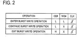
- FIG.2 is a diagram showing states of input signals requesting operation associated with the burst write operation of FIG. 1 , according to one embodiment.
- the operation to enter the burst write operation is requested if the chip enable signal CE# and the write enable signal WE# are both at a low level (L), and the clock signal CLK is on the rising edge.
- the operation to continue the burst write operation is requested if the chip enable signal CE# is at a low level (L), and the clock signal CLK is on the rising edge.
- the logic level of the write enable signal WE# may be left unspecified (X).
- the operation to exit the burst write operation is requested if the chip enable signal CE# is at a high level (H), and the clock signal CLK is on the rising edge.
- the logic level of the write enable signal WE# may be left unspecified (X). Any of the enter burst write operation, continue burst write operation and exit burst write operation is performed by buffering the logic level of the chip enable signal CE# and write enable signal WE# at the time of the rising edge of the clock signal CLK.
- the three operations are requested in synchronization with the clock signal CLK.
- FIG.3 is an operation waveform diagram associated with the burst write operation of FIG. 1 , according to one embodiment.
- clock cycles (1) through (4) represent the duration of a first burst write operation
- clock cycles (5) and (6) represent the duration of a second burst write operation.
- the first burst write operation includes the cycles in which the burst operation is in progress (e.g., clock cycles (1) through (3)), and the following cycle of exiting the burst write operation (e.g., clock cycle (4)).
- the second burst write operation includes the cycle of entering the burst write operation (e.g., clock cycle (5)), and the following cycle in which the burst write operation is in progress (e.g., clock cycle (6)).
- FIG.3 is an operation waveform diagram in case of an immediate shift from the first burst write operation to the second burst write operation.
- the D-type flip-flops 5 and 7 buffer an inverted signal of the chip enable signal CE# and an inverted signal of the write enable signal WE# in synchronization with the clock signal CLK.
- the buffered signals are subjected to the logical operation AND by the AND gate 9. If the chip enable signal CE# and the write enable signal WE# are both at a low level, a high level set signal BWS is output from the AND gate 9 which performs the logical operation AND on the inverted signals of the afore-mentioned signals.
- the latch circuit 11 is set by the high level set signal BWS, thereby setting the burst write mode signal BWM to a high level. With this provision, the operation to enter the burst write operation is accepted. In FIG.2 , this is shown by the enter command to the burst write operation. The default address Am is input at this time as well. In FIG.3 this is shown by clock cycle (5).
- a low level signal is output from the inverted output terminal (BQ) of the latch circuit 11.
- This signal is inverted by the inverter gate 13 into a high level signal, and is input to the reset terminal of the D-type flip flop 5.
- the D-type flip flop 5 is thereby reset, and the output terminal (Q) is held at a low level, regardless of the logic level of the write enable signal WE#.
- the set signal BWS is held at a low level. Accordingly, no set signals BWS are issued with respect to the latch circuit 11 after entering the burst write operation.
- the burst write mode signal BWM which was already set once is reset only by a reset signal BWR.
- the write operation continues after the next cycle (6), provided the low level chip enable signal CE# is buffered in synchronization with an edge of the clock signal CLK of transition to a high level.
- the address corresponding to the memory cell which is written to serves as the address which is incremented in each clock cycle, from the default address Am, by a controller which is not illustrated.
- the burst write operation continues in clock cycles (1) through (3) as well, in a similar manner.
- the low level chip enable signal CE# is buffered in synchronization with an edge of the clock signal CLK of transition to a high level, thereby allowing the write operation to continue.
- Clock cycles (6) and (1) through (3) include commands to continue the burst write operation, as shown in FIG.2 .
- the chip enable signal CE# is set to a high level prior to clock cycle (4).
- the high level chip enable signal CE# is inverted by the inverter gate 3 so as to be buffered in the D-type flip flop 7 in synchronization with the transition of the clock signal CLK to a high level.
- the buffered chip enable signal CE# is output by the inverted output terminal (BQ), as a high level reset signal BWR.
- the latch circuit 11 is reset by the high level reset signal BWR, thereby resetting the burst write mode signal BWM to a low level. With this provision, the operation to exit the burst write operation is accepted. In FIG.2 , this is shown by the exit command from the burst write operation.
- the set signal BWS in response to the command to enter the burst write operation and the reset signal BWR in response to the command to exit the burst write operation are generated with respect to the latch circuit 11.
- the latch circuit 11 latches the state of the burst write operation and outputs the burst write mode signal BWM based on the chip enable signal CE# and the write enable signal WE# which are both buffered in synchronization with the transition of the clock signal CLK to a high level. Any of the enter command, continue command and exit command with respect to the burst write operation is input as a clock signal-synchronized command. This eliminates the need for specific controls, such as separate adjustment of the mutual relationships between commands, and adjustments of timings (e.g., adjustment of input timing), thereby making overall control of command input easier.
- a computer executable method for controlling a burst write operation in a synchronous memory device comprises latching a state for performing the burst write operation, buffering a first control signal for requesting exit from the burst write operation in synchronization with a clock signal associated with the burst write operation, and resetting the state for the performing the burst write operation in response to the buffering of the first control signal, where the first control signal is associated with a chip disable signal.
- FIG.4 is a circuit diagram of an exemplary synchronous memory device for controlling a burst write operation, according to one embodiment.
- FIG. 4 describes a case where both the enter command and the exit command are set in response to a combination of a plurality of control signals.
- the respective control signals are sent to D-type flip flop groups 21 and 23.
- the D-type flip flop groups 21 and 23 have a structure comprising a D-type flip flop for each control signal, and they buffer each control signal in synchronization with the transition of the clock signal CLK to a high level.
- the control signal buffered in the D-type flip flop group 21 in response to the enter command is input to a set decoder 25 for decoding.
- the control signal buffered in the D-type flip flop group 23 in response to the exit command is input to a reset decoder 27 for decoding.
- a set signal BWS and a reset signal BWR are respectively output from the set decoder 25 and reset decoder 27 to set/reset the latch circuit 11.
- FIG. 5 is a circuit diagram of an exemplary synchronous memory device for controlling a burst write operation, according to one embodiment.
- control signals for setting the exit command are respectively sent to the D-type flip flops 5 and 7.
- the inverted output terminals (BQ) of the D-type flip flops 5 and 7 are input to an OR circuit 31, and the output of the OR circuit 31 is input to the reset terminal (R) of the latch circuit 11.
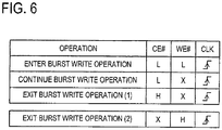
- the reset signal BWR is generated in response to a high level of either one of the chip enable signal CE# or the write enable signal WE# on the rising edge of the clock signal CLK.
- the latch circuit 11 is reset in response to the high level reset signal BWR, thereby resetting the burst write mode signal BWM to a low level. With this provision, the operation to exit the burst write operation is accepted. In FIG.6 , this is shown by the exit command 1 or 2 with respect to the burst write operation.
- the respective control signals which are latched in the D-type flip flops 5 and 7 in response to the clock signal CLK are subjected to logical operations in the logic circuits 9 and 31.
- the resulting output signals are input to the latch circuit 11, thereby making it possible to set/hold the configuration with the clock signal CLK, so as to accommodate high frequencies.
- FIG.7 is a circuit diagram of an exemplary synchronous memory device for controlling a burst write operation, according to one embodiment.
- the burst write operation is requested by the chip enable signal CE# and the write enable signal WE#, and further, exit from the burst write operation is requested by either one of the two control signals.
- the write enable signal WE# and the chip enable signal CE# forwarded to the synchronous memory device are respectively input to the logic circuits 41 and 42.
- the output terminal of the logic circuit 42 is connected to the input terminal (D) of the D-type flip flop 46.
- the output terminal of the logic circuit 41 is input to a delay circuit 43 corresponding to the amount of delay by the D-type flip flop 46, and the output BWS of the delay circuit 43 is connected to the input terminal (D) of a set terminal-equipped D-type flip flop 45.
- the synchronizing terminal (CK) of the D-type flip flop 46 is supplied with a clock signal CLK.
- the synchronizing terminal (CK) of the set terminal-equipped D-type flip flop 45 is supplied with the clock signal CLK through a delay circuit 44 corresponding to the amount of delay by the D-type flip flop 46.
- the output terminal (Q) of the D-type flip flop 46 is connected to the reset terminal (R) of the set terminal-equipped D-type flip flop 45.
- the output terminal (Q) of the set terminal-equipped-D-type flip flop 45 is connected to the set terminal (SET) of the set terminal-equipped D-type flip flop 45.
- the set terminal-equipped D-type flip flop 45 buffers the signal BWS resulting from the logical operation between the chip enable signal CE# and the write enable signal WE#, in synchronization with the clock signal CLK.
- the buffered signal BWS is simultaneously an output to the output terminal BWM of the set terminal-equipped D-type flip flop 45, and an input to the set terminal (SET). If the chip enable signal CE# and the write enable signal WE# are both at low level, the burst write mode signal BWM is set to a high level so that the burst write mode signal BWM is held at a high level, regardless of the information on the input terminal (D) from the set terminal (SET).
- the D-type flip flop 46 buffers the signal resulting from the logical operation between the chip enable signal CE# or the write enable signal WE# in synchronization with the clock signal CLK.
- the reset signal BWR to be output is input to the reset terminal of the set terminal-equipped D-type flip flop 45. If either the chip enable signal CE# or the write enable signal WE# is at a high level, the burst write mode signal BWM is reset to a low level.
- the logic circuit 41 that makes a decision on a plurality of external control signals to generate the set signal is arranged before the clock-controlled set terminal-equipped D-type flip flop 45.
- the setting information for the burst write mode signal BWM is generated at a high speed.
- the hold function for the state of the set signal can be set at high speed. This is due to the fact that the signal BMW latched in response to the clock signal CLK is fed-back to the functional circuit 45 itself.
- the logic circuit 42 that makes a decision on a plurality of external control signals for generating the reset signal is arranged before the clock-controlled D-type flip flop 46. As a result, the reset information for the burst write mode signal BWM is output at a high speed.
- the D-type flip flop As having a circuit configuration for buffering the control signal in synchronization with the clock signal, the present invention is not limited to this. Any circuit configuration which can buffer signals in synchronization with the clock signal may be employed. Also, although a description was given of the synchronizing timing as the timing at which the clock signal transits to a high level, it is needless to say the timing of transition to a low level may also be employed.
Landscapes
- Dram (AREA)
- Static Random-Access Memory (AREA)
- Read Only Memory (AREA)
Description
- This application claims priority from Japanese patent application
2007-187763 filed on July 19, 2007 - The present invention relates to semiconductor devices and methods, particularly to synchronous memory devices and control methods for performing burst mode operations.
- A burst mode operation enables a high-speed synchronous read and/or write operation in a memory device. The burst mode operation involves a multi clock sequence performed in an ordered fashion. The start operation and continue operation with respect to the burst write operation in a synchronous memory device are performed in synchronization with a clock signal or sync signal. On the other hand, an exit operation from the burst write operation is controlled by an asynchronous signal. For instance, in a flash memory, the exit operation is initiated by an asynchronous transition of a chip enable signal from a low level to a high level. However, when the exit operation from the burst write operation is performed asynchronously at the last cycle of the burst write operation, there is a risk that the last cycle of the write operation may be terminated prematurely. To prevent the overlapping of the last cycle of the burst write operation with the exit operation, a control signal requesting an exit from the burst write operation needs to be inhibited for a fixed time interval until the burst write operation is fully completed.
- However, if the cycle of the sync signal at a higher frequency is longer than the hold time, there may be cases where a wait time period or a wait cycle must be provided during the period from exiting the burst write operation until moving into the next operation cycle. Implementing a fix for the cases makes the control of the burst mode operation more complex.
PublishedUS patent application 2005/0265088 discloses a memory device that includes a memory array; a set of write registers; an input buffer designed to sequentially receive a series of write data during a burst cycle, and to write said write data into associated ones of said write registers; a write release register containing a set of write release flags associated with said write registers, respectively; a write release register controller asserting associated ones of said write release flags in response to said write data being written into said associated ones of said write registers; and a write amplifier designed to concurrently write said write data contained in said write registers associated with asserted ones of said write release flags, selectively, when said burst cycle is aborted in response to a control signal. - The invention is defined in the appended claims. This summary is provided to introduce a selection of concepts in a simplified form that are further described below in the detailed description. This summary is not intended to identify key features or essential features of the claimed subject matter, nor is it intended to be used to limit the scope of the claimed subject matter.
- One embodiment of the present invention is directed to a synchronous memory device for controlling a burst write operation which comprises a first buffer circuit for buffering a first control signal requesting an exit from the burst write operation in synchronization with a clock signal associated with the burst write operation, and a latch circuit for performing a reset in response to the first control signal forwarded by the first buffer circuit, wherein the reset triggers the exit from the burst write operation.
- Another embodiment of the present invention is directed to a synchronous memory device for controlling a burst write operation which comprises a first flip flop circuit for buffering an enter command for the burst write operation in synchronization with a clock signal associated with the burst operation, and a second flip flop circuit for buffering an exit command for the burst write operation in synchronization with the clock signal. The device further comprises a reset decoder for decoding the exit command forwarded by the second flip flop circuit, and a latch circuit for performing a reset in response to the exit command forwarded by the reset decoder.
- Yet another embodiment of the present invention is directed to a synchronous memory device for controlling a burst write operation which comprises a first logic circuit and a second logic circuit for generating a set trigger signal and a reset trigger signal, respectively, by performing a logical operation between a chip enable signal and a write enable signal associated with the burst write operation. The device further comprises a first flip flop circuit for buffering the reset trigger signal of the second logic circuit in synchronization with a clock signal associated with the burst write operation, and a second flip flop circuit for buffering the set trigger signal of the first logic circuit in synchronization with the clock signal.
- As will be illustrated in the detailed description, other embodiments pertain to control systems, methods, and devices for synchronous memory devices which are capable of performing an exit operation from a burst write operation in sync with a clock signal associated with the burst write operation. This enables the operations of the exit operation as well as other burst mode operations, such as a start operation, a continue operation, and so on, to be in sync with each other. Thus, the burst write operation can be completed without being cut short by the exit operation since a command for triggering the exit operation is processed in synchronization with the clock signal. Accordingly, the feature eliminates a need for inhibiting the exit operation until the last cycle of the burst write operation is completed using a complex control scheme as recited by the conventional art.
- Example embodiments are illustrated by way of example and not limitation in the figures of the accompanying drawings, in which like references indicate similar elements and in which:
-
FIG.1 is a circuit diagram of an exemplary synchronous memory device for controlling a burst write operation, according to one embodiment. -
FIG.2 is a diagram showing states of input signals requesting operation associated with the burst write operation ofFIG. 1 , according to one embodiment. -
FIG.3 is an operation waveform diagram associated with the burst write operation ofFIG. 1 , according to one embodiment. -
FIG.4 is a circuit diagram of an exemplary synchronous memory device for controlling a burst write operation, according to one embodiment. -
FIG. 5 is a circuit diagram of an exemplary synchronous memory device for controlling a burst write operation, according to one embodiment. -
FIG.6 is a diagram showing states of input signals requesting operation associated with the burst write operation ofFIG. 5 , according to one embodiment. -
FIG.7 is a circuit diagram of an exemplary synchronous memory device for controlling a burst write operation, according to one embodiment. - Other features of the present embodiments will be apparent from the accompanying drawings and from the detailed description that follows.
- Reference will now be made in detail to the preferred embodiments of the invention, examples of which are illustrated in the accompanying drawings. While the invention will be described in conjunction with the preferred embodiments, it will be understood that they are not intended to limit the invention to these embodiments. On the contrary, the invention is intended to cover alternatives, modifications and equivalents, which may be included within the spirit and scope of the invention as defined by the claims. Furthermore, in the detailed description of the present invention, numerous specific details are set forth in order to provide a thorough understanding of the present invention. However, it will be obvious to one of ordinary skill in the art that the present invention may be practiced without these specific details. In other instances, well known methods, procedures, components, and circuits have not been described in detail as not to unnecessarily obscure aspects of the present invention.
- Some portions of the detailed descriptions that follow are presented in terms of procedures, logic blocks, processing, and other symbolic representations for fabricating semiconductor devices. These descriptions and representations are the means used by those skilled in the art of semiconductor device fabrication to most effectively convey the substance of their work to others skilled in the art. A procedure, logic block, process, etc., is herein, and generally, conceived to be a self-consistent sequence of steps or instructions leading to a desired result. The steps are those requiring physical manipulations of physical quantities. Unless specifically stated otherwise as apparent from the following discussions, is appreciated that throughout the present application, discussions utilizing terms such as "forming," "performing," "producing," "depositing," or "etching," or the like, refer to actions and processes of semiconductor device fabrication.
- Briefly stated, embodiments pertain to control systems, methods, and devices for synchronous memory devices which are capable of performing an exit operation from a burst write operation in sync with a clock signal associated with the burst write operation. This enables the operations of the exit operation as well as other operations, such as a start operation, a continue operation, and so on, associated with the burst write operation to be in sync with each other. Thus, the burst write operation can be completed without being cut short by the exit operation since a command for triggering the exit operation is processed in synchronization with the clock signal. Accordingly, the feature eliminates a need for inhibiting the exit operation until the last cycle of the burst write operation is completed using a complex control scheme as recited by the conventional art.
-
FIG.1 is a circuit diagram of an exemplary synchronous memory device for controlling a burst write operation, according to one embodiment. In one exemplary implementation, a burst write operation is requested by a first control signal (e.g., a chip enable single CE#) and a second control signal (e.g., a write enable signal WE#). The write enable signal WE# and the chip enable signal CE# are processed through aninverter gate 1 and aninverter gate 3, respectively. Output terminals of theinverter gates flops flops AND gate 9 is connected to a set terminal (S) of alatch circuit 11. An inverted output terminal (BQ) of the D-type flip-flop 7 is connected to a reset terminal (R) of thelatch circuit 11. The inverted output terminal (BQ) of thelatch circuit 11 is connected to the reset terminal (BR) of the D-type flip-flop 5 through aninverter gate 13. A set signal BWS is output from theAND gate 9, and a reset signal BWR is output from the inverted output terminal (BQ) of the D-type flip-flop 7. A burst write mode signal BWM indicative of the burst write operation state is output from the output terminal (Q) of thelatch circuit 11. -
FIG.2 is a diagram showing states of input signals requesting operation associated with the burst write operation ofFIG. 1 , according to one embodiment. With respect toFIG. 1 , the operation to enter the burst write operation is requested if the chip enable signal CE# and the write enable signal WE# are both at a low level (L), and the clock signal CLK is on the rising edge. The operation to continue the burst write operation is requested if the chip enable signal CE# is at a low level (L), and the clock signal CLK is on the rising edge. In this case, the logic level of the write enable signal WE# may be left unspecified (X). The operation to exit the burst write operation is requested if the chip enable signal CE# is at a high level (H), and the clock signal CLK is on the rising edge. In this case, the logic level of the write enable signal WE# may be left unspecified (X). Any of the enter burst write operation, continue burst write operation and exit burst write operation is performed by buffering the logic level of the chip enable signal CE# and write enable signal WE# at the time of the rising edge of the clock signal CLK. The three operations are requested in synchronization with the clock signal CLK. -
FIG.3 is an operation waveform diagram associated with the burst write operation ofFIG. 1 , according to one embodiment. InFIG.3 , clock cycles (1) through (4) represent the duration of a first burst write operation, and clock cycles (5) and (6) represent the duration of a second burst write operation. The first burst write operation includes the cycles in which the burst operation is in progress (e.g., clock cycles (1) through (3)), and the following cycle of exiting the burst write operation (e.g., clock cycle (4)). The second burst write operation includes the cycle of entering the burst write operation (e.g., clock cycle (5)), and the following cycle in which the burst write operation is in progress (e.g., clock cycle (6)).FIG.3 is an operation waveform diagram in case of an immediate shift from the first burst write operation to the second burst write operation. - In
FIG.1 , the D-type flip-flops gate 9. If the chip enable signal CE# and the write enable signal WE# are both at a low level, a high level set signal BWS is output from the ANDgate 9 which performs the logical operation AND on the inverted signals of the afore-mentioned signals. Thelatch circuit 11 is set by the high level set signal BWS, thereby setting the burst write mode signal BWM to a high level. With this provision, the operation to enter the burst write operation is accepted. InFIG.2 , this is shown by the enter command to the burst write operation. The default address Am is input at this time as well. InFIG.3 this is shown by clock cycle (5). - Upon entering the burst write operation and setting the burst write mode signal BWM, a low level signal is output from the inverted output terminal (BQ) of the
latch circuit 11. This signal is inverted by theinverter gate 13 into a high level signal, and is input to the reset terminal of the D-type flip flop 5. The D-type flip flop 5 is thereby reset, and the output terminal (Q) is held at a low level, regardless of the logic level of the write enable signal WE#. With this, the set signal BWS is held at a low level. Accordingly, no set signals BWS are issued with respect to thelatch circuit 11 after entering the burst write operation. In other words, the burst write mode signal BWM which was already set once is reset only by a reset signal BWR. - The write operation continues after the next cycle (6), provided the low level chip enable signal CE# is buffered in synchronization with an edge of the clock signal CLK of transition to a high level. The address corresponding to the memory cell which is written to serves as the address which is incremented in each clock cycle, from the default address Am, by a controller which is not illustrated.
- The burst write operation continues in clock cycles (1) through (3) as well, in a similar manner. The low level chip enable signal CE# is buffered in synchronization with an edge of the clock signal CLK of transition to a high level, thereby allowing the write operation to continue. Clock cycles (6) and (1) through (3) include commands to continue the burst write operation, as shown in
FIG.2 . - The chip enable signal CE# is set to a high level prior to clock cycle (4). The high level chip enable signal CE# is inverted by the
inverter gate 3 so as to be buffered in the D-type flip flop 7 in synchronization with the transition of the clock signal CLK to a high level. The buffered chip enable signal CE# is output by the inverted output terminal (BQ), as a high level reset signal BWR. Thelatch circuit 11 is reset by the high level reset signal BWR, thereby resetting the burst write mode signal BWM to a low level. With this provision, the operation to exit the burst write operation is accepted. InFIG.2 , this is shown by the exit command from the burst write operation. - The set signal BWS in response to the command to enter the burst write operation and the reset signal BWR in response to the command to exit the burst write operation are generated with respect to the
latch circuit 11. Thelatch circuit 11 latches the state of the burst write operation and outputs the burst write mode signal BWM based on the chip enable signal CE# and the write enable signal WE# which are both buffered in synchronization with the transition of the clock signal CLK to a high level. Any of the enter command, continue command and exit command with respect to the burst write operation is input as a clock signal-synchronized command. This eliminates the need for specific controls, such as separate adjustment of the mutual relationships between commands, and adjustments of timings (e.g., adjustment of input timing), thereby making overall control of command input easier. - In one embodiment, a computer executable method for controlling a burst write operation in a synchronous memory device comprises latching a state for performing the burst write operation, buffering a first control signal for requesting exit from the burst write operation in synchronization with a clock signal associated with the burst write operation, and resetting the state for the performing the burst write operation in response to the buffering of the first control signal, where the first control signal is associated with a chip disable signal.
-
FIG.4 is a circuit diagram of an exemplary synchronous memory device for controlling a burst write operation, according to one embodiment.FIG. 4 describes a case where both the enter command and the exit command are set in response to a combination of a plurality of control signals. In this embodiment, the respective control signals are sent to D-typeflip flop groups flip flop groups flip flop group 21 in response to the enter command is input to aset decoder 25 for decoding. The control signal buffered in the D-typeflip flop group 23 in response to the exit command is input to areset decoder 27 for decoding. A set signal BWS and a reset signal BWR are respectively output from theset decoder 25 and resetdecoder 27 to set/reset thelatch circuit 11. - Also, even in the case that the enter command and exit command with respect to the burst write operation are input in response to a combination of a plurality of control signals, if each of the control signals is buffered in synchronization with the clock signal CLK, and the buffered control signals are decoded, it is possible to obtain clock signal CLK-synchronized operations in response to any of the enter command, continue command and exit command.
-
FIG. 5 is a circuit diagram of an exemplary synchronous memory device for controlling a burst write operation, according to one embodiment. InFIG. 5 , control signals for setting the exit command are respectively sent to the D-type flip flops type flip flops OR circuit 31, and the output of theOR circuit 31 is input to the reset terminal (R) of thelatch circuit 11. The reset signal BWR is generated in response to a high level of either one of the chip enable signal CE# or the write enable signal WE# on the rising edge of the clock signal CLK. Thelatch circuit 11 is reset in response to the high level reset signal BWR, thereby resetting the burst write mode signal BWM to a low level. With this provision, the operation to exit the burst write operation is accepted. InFIG.6 , this is shown by theexit command - In one embodiment, the respective control signals which are latched in the D-
type flip flops logic circuits latch circuit 11, thereby making it possible to set/hold the configuration with the clock signal CLK, so as to accommodate high frequencies. -
FIG.7 is a circuit diagram of an exemplary synchronous memory device for controlling a burst write operation, according to one embodiment. InFIG. 7 , the burst write operation is requested by the chip enable signal CE# and the write enable signal WE#, and further, exit from the burst write operation is requested by either one of the two control signals. The write enable signal WE# and the chip enable signal CE# forwarded to the synchronous memory device (not illustrated) are respectively input to thelogic circuits logic circuit 42 is connected to the input terminal (D) of the D-type flip flop 46. The output terminal of thelogic circuit 41 is input to adelay circuit 43 corresponding to the amount of delay by the D-type flip flop 46, and the output BWS of thedelay circuit 43 is connected to the input terminal (D) of a set terminal-equipped D-type flip flop 45. The synchronizing terminal (CK) of the D-type flip flop 46 is supplied with a clock signal CLK. The synchronizing terminal (CK) of the set terminal-equipped D-type flip flop 45 is supplied with the clock signal CLK through adelay circuit 44 corresponding to the amount of delay by the D-type flip flop 46. The output terminal (Q) of the D-type flip flop 46 is connected to the reset terminal (R) of the set terminal-equipped D-type flip flop 45. The output terminal (Q) of the set terminal-equipped-D-type flip flop 45 is connected to the set terminal (SET) of the set terminal-equipped D-type flip flop 45. - In
FIG. 7 , the set terminal-equipped D-type flip flop 45 buffers the signal BWS resulting from the logical operation between the chip enable signal CE# and the write enable signal WE#, in synchronization with the clock signal CLK. The buffered signal BWS is simultaneously an output to the output terminal BWM of the set terminal-equipped D-type flip flop 45, and an input to the set terminal (SET). If the chip enable signal CE# and the write enable signal WE# are both at low level, the burst write mode signal BWM is set to a high level so that the burst write mode signal BWM is held at a high level, regardless of the information on the input terminal (D) from the set terminal (SET). The D-type flip flop 46 buffers the signal resulting from the logical operation between the chip enable signal CE# or the write enable signal WE# in synchronization with the clock signal CLK. The reset signal BWR to be output is input to the reset terminal of the set terminal-equipped D-type flip flop 45. If either the chip enable signal CE# or the write enable signal WE# is at a high level, the burst write mode signal BWM is reset to a low level. - Here, the
logic circuit 41 that makes a decision on a plurality of external control signals to generate the set signal is arranged before the clock-controlled set terminal-equipped D-type flip flop 45. As a result, the setting information for the burst write mode signal BWM is generated at a high speed. In addition, the hold function for the state of the set signal can be set at high speed. This is due to the fact that the signal BMW latched in response to the clock signal CLK is fed-back to thefunctional circuit 45 itself. In addition, thelogic circuit 42 that makes a decision on a plurality of external control signals for generating the reset signal is arranged before the clock-controlled D-type flip flop 46. As a result, the reset information for the burst write mode signal BWM is output at a high speed. - The present invention is not limited to the above-described embodiments, and various improvements and modifications thereof are applicable without departing from the spirit and scope of the present invention. For instance, while the above-described embodiments describe an example in which the enter command and the exit command are buffered in synchronization with the clock signal, other commands can be buffered in synchronization with the clock signal.
- Although a description was given of the D-type flip flop as having a circuit configuration for buffering the control signal in synchronization with the clock signal, the present invention is not limited to this. Any circuit configuration which can buffer signals in synchronization with the clock signal may be employed. Also, although a description was given of the synchronizing timing as the timing at which the clock signal transits to a high level, it is needless to say the timing of transition to a low level may also be employed.
Claims (14)
- A synchronous memory device for controlling a burst write operation, comprising:a first flip-flop circuit (7) for buffering chip enable signal (CE#) in synchronization with a clock signal (CLK) associated with the burst write operation;a second flip-flop circuit (5) for buffering a write enable signal (WE#) in synchronization with the clock signal (CLK);logic circuit (9) coupled to receive the buffered chip enable signal and write enable signal output from the first and second flip-flop circuits and configured to generate a burst write set signal (BWS); andan SR-latch circuit (11) coupled to receive the burst write set signal (BWS) and a burst reset signal (BWR) from an inverted output of the first flip-flop circuit, and configured to output a burst mode signal (BWM),wherein the activation of the burst mode signal (BWM) triggers entry into the burst write mode, and deactivation of the burst mode signal triggers exit from the burst write operation, andwherein the burst mode signal is input to a reset input of the second flip-flop circuit so that the burst mode signal is held active regardless of the state of the write enable signal (WE#).
- The synchronous memory device according to claim 1, wherein the SR-latch circuit (11) is set for triggering the entry to the burst write operation in response to the write enable signal (WE#) when the chip enable signal is not active.
- The synchronous memory device according to claim 2, further comprising an inverter (13) coupled between an output terminal of the latch circuit (11) and a reset terminal of the second flip-flop circuit (5), wherein a control signal through the inverter (13) prevents the second flip-flop circuit (5) from buffering the write enable signal (WE#) during the burst write operation.
- The synchronous memory device according to claim 3, further comprising a first inverter (3) coupled to an input terminal of the first flip-flop circuit (7), and a second inverter (1) coupled to an input terminal of the second flip-flop circuit (5),
wherein the logic circuit comprises an AND gate (9) coupled to a set terminal of the SR-latch circuit (11) for performing an AND operation of a chip enable signal of the first flip-flop circuit (7) and a write enable signal of the second flip-flop circuit (5). - A synchronous memory device for controlling a burst write operation, comprising:a first flip-flop circuit (7) for buffering chip enable signal (CE#) in synchronization with a clock signal (CLK) associated with the burst write operation;a second flip-flop circuit (5) for buffering a write enable signal (WE#) in synchronization with the clock signal (CLK);logic circuit (9) coupled to receive the buffered chip enable signal and write enable signal output from the first and second flip-flop circuits and configured to generate a burst write set signal (BWS);second logic circuit (31) coupled to receive the buffered chip enable signal and write enable signal output from the first and second flip-flop circuits and configured to generate a burst reset signal (BWR); andan SR-latch circuit (11) coupled to receive the burst write set signal (BWS) and the burst reset signal (BWR), and configured to output a burst mode signal (BWM),wherein the activation of the burst mode signal (BWM) triggers entry into the burst write mode, and deactivation of the burst mode signal triggers exit from the burst write operation.
- The synchronous memory device of claim 5, wherein the second logic circuit (31) comprises a OR gate.
- A synchronous memory device for controlling a burst write operation, comprising:a first logic circuit (41, 43) and a second logic circuit (42) for generating a burst write set trigger signal and a reset trigger signal, respectively, by performing a logical operation between a chip enable signal (CE#) and a write enable signal (WE#) associated with the burst write operation;a first flip-flop circuit (46) for buffering the reset trigger signal of the second logic circuit (42) in synchronization with a clock signal (CLK) associated with the burst write operation and for outputting a burst write reset trigger signal (BWR); anda second flip-flop circuit (45) for buffering the burst write set trigger signal of the first logic circuit (41) in synchronization with the clock signal (CLK) and for outputting a burst mode signal (BWM) for controlling the burst write operation,wherein the second flip-flop circuit (45) includes a data input (D) for receiving said burst write set trigger signal, a set input (SET) for receiving said burst write mode signal and a reset input (R) for receiving said burst write reset trigger signal, wherein (i) an active signal at the set input operates to hold the burst mode signal in a high level regardless of the signal at the data input, and (ii) an active signal at the reset input operates to switch the burst mode signal to a low level.
- The synchronous memory device according to claim 7, wherein the first logic circuit (41) comprises an NOR gate.
- The synchronous memory device according to claim 7, wherein the second logic circuit (42) comprises an OR gate.
- The synchronous memory device according to claim 7, further comprising a delay element (42) coupled between the first logic circuit (41) and the data input of the second flip-flop circuit (45) and a delay element (44) coupled between the clock and a clock terminal of the second flip-flop circuit (45).
- A method for controlling a burst write operation in a synchronous memory device, the method comprising:buffering a chip enable signal (CE#) in synchronization with a clock signal (CLK) associated with the burst write operation;buffering a write enable signal (WE#) in synchronization with a clock signal (CLK) associated with the burst write operation;performing a logical operation on the buffered chip enable signal and write enable signal to generate a burst write set signal (BWS);generating a burst mode signal (BWM) based upon the burst write signal and a burst write reset trigger signal (BWR),wherein the activation of the burst mode signal (BWM) triggers entry into the burst write mode, and deactivation of the burst mode signal triggers exit from the burst write operation, andwherein buffering a write enable signal comprises inputting the burst mode signal to a reset input of a flip-flop circuit of the synchronous memory device operable to buffer the write enable signal, whereby the burst mode signal is held active regardless of the state of the write enable signal (WE#).
- The method according to claim 11, wherein the chip enable signal (CE#) is associated with a chip disable signal.
- A method for controlling a burst write operation in a synchronous memory device, the method comprising:generating a burst write set trigger signal and a reset trigger signal, respectively, by performing a logical operation between a chip enable signal (CE#) and a write enable signal (WE# associated with the burst write operation;buffering, at a first flip-flop circuit (46), the reset trigger signal in synchronization with a clock signal (CLK) associated with the burst write operation;outputting, at the first flip-flop circuit (46), a burst write reset trigger signal (BWR);buffering, at a second flip flop circuit (45), the burst write set trigger signal at a data input in synchronization with a clock signal, the buffered reset trigger signal at a reset input, and a set input signal, the second flip-flop circuit (45) operable to output a burst mode signal for controlling the burst write operation,wherein said burst write set trigger signal is received at a data input (D) of the second flip flop circuit (45), said burst write mode signal is received at a set input (SET) of the second flip flop circuit (45), and said burst write reset trigger signal is received at a reset input (R) of the second flip flop circuit (45), andwherein (i) an active signal at the set input of the second flip-flop (45) operates to hold the burst mode signal in a high level regardless of the signal at the data input, and (ii) an active signal at the reset input of the second flip-flop (45) operates to switch the burst mode signal to a low level.
- The method according to claim 13, wherein
generating a set trigger signal comprises performing a logical NOR operation between said chip and write enable signals (CE#, WE#), and
generating a reset trigger signal comprises performing a logical OR operation between said chip and write enable signals (CE#, WE#).
Applications Claiming Priority (2)
| Application Number | Priority Date | Filing Date | Title |
|---|---|---|---|
| JP2007187763A JP2009026370A (en) | 2007-07-19 | 2007-07-19 | Synchronous type storage device and its control method |
| PCT/US2008/008864 WO2009014678A1 (en) | 2007-07-19 | 2008-07-21 | Synchronous memory devices and control methods for performing burst write operations |
Publications (2)
| Publication Number | Publication Date |
|---|---|
| EP2171719A1 EP2171719A1 (en) | 2010-04-07 |
| EP2171719B1 true EP2171719B1 (en) | 2019-01-23 |
Family
ID=40032431
Family Applications (1)
| Application Number | Title | Priority Date | Filing Date |
|---|---|---|---|
| EP08780275.7A Not-in-force EP2171719B1 (en) | 2007-07-19 | 2008-07-21 | Synchronous memory devices and control methods for performing burst write operations |
Country Status (7)
| Country | Link |
|---|---|
| US (1) | US7821842B2 (en) |
| EP (1) | EP2171719B1 (en) |
| JP (1) | JP2009026370A (en) |
| KR (1) | KR101205589B1 (en) |
| CN (1) | CN101755304B (en) |
| TW (1) | TWI407449B (en) |
| WO (1) | WO2009014678A1 (en) |
Families Citing this family (4)
| Publication number | Priority date | Publication date | Assignee | Title |
|---|---|---|---|---|
| US8552765B2 (en) | 2011-01-07 | 2013-10-08 | Stmicroelectronics International N.V. | Adaptive multi-stage slack borrowing for high performance error resilient computing |
| JP4988048B1 (en) | 2011-02-14 | 2012-08-01 | 株式会社東芝 | Semiconductor memory device |
| US9444440B2 (en) * | 2011-06-30 | 2016-09-13 | Stmicroelectronics International N.V. | Transition detector |
| CN112202446B (en) * | 2019-07-08 | 2024-06-14 | 北京三中科技有限公司 | Phase synchronization device and method |
Family Cites Families (9)
| Publication number | Priority date | Publication date | Assignee | Title |
|---|---|---|---|---|
| KR970001699B1 (en) | 1994-03-03 | 1997-02-13 | 삼성전자 주식회사 | Syncronous semiconductor memory device having the function of automatic precharge |
| JP3843145B2 (en) * | 1995-12-25 | 2006-11-08 | 株式会社ルネサステクノロジ | Synchronous semiconductor memory device |
| JP3708729B2 (en) * | 1998-11-18 | 2005-10-19 | 富士通株式会社 | Semiconductor memory device |
| IT1318978B1 (en) * | 2000-10-06 | 2003-09-19 | St Microelectronics Srl | CONTROL STRUCTURE AND TIMING FOR A MEMORY |
| JP3959341B2 (en) * | 2002-02-18 | 2007-08-15 | 株式会社東芝 | Semiconductor integrated circuit device |
| JP2004212749A (en) | 2003-01-07 | 2004-07-29 | Hitachi Ltd | Display device and driving method thereof |
| JP4492938B2 (en) * | 2004-05-26 | 2010-06-30 | ルネサスエレクトロニクス株式会社 | Semiconductor memory device and operation method thereof |
| JP4216778B2 (en) * | 2004-07-12 | 2009-01-28 | 株式会社ルネサステクノロジ | Semiconductor device |
| JP4830495B2 (en) | 2006-01-11 | 2011-12-07 | ソニー株式会社 | Self-luminous display device, conversion table update device, and program |
-
2007
- 2007-07-19 JP JP2007187763A patent/JP2009026370A/en active Pending
-
2008
- 2008-06-12 TW TW097121850A patent/TWI407449B/en not_active IP Right Cessation
- 2008-07-21 WO PCT/US2008/008864 patent/WO2009014678A1/en not_active Ceased
- 2008-07-21 KR KR1020107001158A patent/KR101205589B1/en not_active Expired - Fee Related
- 2008-07-21 CN CN2008800252325A patent/CN101755304B/en active Active
- 2008-07-21 US US12/176,997 patent/US7821842B2/en active Active
- 2008-07-21 EP EP08780275.7A patent/EP2171719B1/en not_active Not-in-force
Non-Patent Citations (1)
| Title |
|---|
| None * |
Also Published As
| Publication number | Publication date |
|---|---|
| JP2009026370A (en) | 2009-02-05 |
| KR20100034014A (en) | 2010-03-31 |
| WO2009014678A1 (en) | 2009-01-29 |
| US7821842B2 (en) | 2010-10-26 |
| CN101755304A (en) | 2010-06-23 |
| US20090207672A1 (en) | 2009-08-20 |
| KR101205589B1 (en) | 2012-11-27 |
| TWI407449B (en) | 2013-09-01 |
| CN101755304B (en) | 2013-03-13 |
| TW200912953A (en) | 2009-03-16 |
| EP2171719A1 (en) | 2010-04-07 |
Similar Documents
| Publication | Publication Date | Title |
|---|---|---|
| US6643215B2 (en) | Synchronous memory devices with synchronized latency control circuits and methods of operating same | |
| KR100540487B1 (en) | Data output control circuit | |
| US20070297250A1 (en) | Data processing apparatus and method using FIFO device | |
| US7586337B2 (en) | Circuit for switching between two clock signals independently of the frequency of the clock signals | |
| JP4751178B2 (en) | Synchronous semiconductor device | |
| US20190026241A1 (en) | Peripheral interface circuit for serial memory | |
| KR100625296B1 (en) | Latency control device and method for controlling the synchronous semiconductor device for high frequency operation | |
| US7007186B1 (en) | Systems and methods for synchronizing a signal across multiple clock domains in an integrated circuit | |
| WO2009060096A1 (en) | Glitch free 2-way clock switch | |
| US10802721B2 (en) | Memory devices configured to latch data for output in response to an edge of a clock signal generated in response to an edge of another clock signal | |
| US7821842B2 (en) | Synchronous memory devices and control methods for performing burst write operations | |
| KR20030028697A (en) | Semiconductor device and semiconductor memory device | |
| US12154634B2 (en) | Data path circuit and method | |
| KR100389038B1 (en) | Synchronous sram device with late write function | |
| JP3087734B2 (en) | Clock signal generation circuit | |
| JP4684561B2 (en) | Semiconductor memory | |
| KR100748461B1 (en) | Data input circuit and method of semiconductor memory device | |
| US12216488B2 (en) | Systems and methods for asynchronous finite machines | |
| KR100656469B1 (en) | Power-Down Controller of Semiconductor Memory | |
| JP2005322036A (en) | Semiconductor device | |
| JPH0199155A (en) | Ready signal generation system |
Legal Events
| Date | Code | Title | Description |
|---|---|---|---|
| PUAI | Public reference made under article 153(3) epc to a published international application that has entered the european phase |
Free format text: ORIGINAL CODE: 0009012 |
|
| 17P | Request for examination filed |
Effective date: 20100113 |
|
| AK | Designated contracting states |
Kind code of ref document: A1 Designated state(s): AT BE BG CH CY CZ DE DK EE ES FI FR GB GR HR HU IE IS IT LI LT LU LV MC MT NL NO PL PT RO SE SI SK TR |
|
| AX | Request for extension of the european patent |
Extension state: AL BA MK RS |
|
| DAX | Request for extension of the european patent (deleted) | ||
| 17Q | First examination report despatched |
Effective date: 20110711 |
|
| RAP1 | Party data changed (applicant data changed or rights of an application transferred) |
Owner name: CYPRESS SEMICONDUCTOR CORPORATION |
|
| GRAP | Despatch of communication of intention to grant a patent |
Free format text: ORIGINAL CODE: EPIDOSNIGR1 |
|
| STAA | Information on the status of an ep patent application or granted ep patent |
Free format text: STATUS: GRANT OF PATENT IS INTENDED |
|
| INTG | Intention to grant announced |
Effective date: 20180622 |
|
| GRAJ | Information related to disapproval of communication of intention to grant by the applicant or resumption of examination proceedings by the epo deleted |
Free format text: ORIGINAL CODE: EPIDOSDIGR1 |
|
| STAA | Information on the status of an ep patent application or granted ep patent |
Free format text: STATUS: EXAMINATION IS IN PROGRESS |
|
| INTC | Intention to grant announced (deleted) | ||
| GRAR | Information related to intention to grant a patent recorded |
Free format text: ORIGINAL CODE: EPIDOSNIGR71 |
|
| GRAS | Grant fee paid |
Free format text: ORIGINAL CODE: EPIDOSNIGR3 |
|
| STAA | Information on the status of an ep patent application or granted ep patent |
Free format text: STATUS: GRANT OF PATENT IS INTENDED |
|
| GRAA | (expected) grant |
Free format text: ORIGINAL CODE: 0009210 |
|
| STAA | Information on the status of an ep patent application or granted ep patent |
Free format text: STATUS: THE PATENT HAS BEEN GRANTED |
|
| INTG | Intention to grant announced |
Effective date: 20181212 |
|
| AK | Designated contracting states |
Kind code of ref document: B1 Designated state(s): AT BE BG CH CY CZ DE DK EE ES FI FR GB GR HR HU IE IS IT LI LT LU LV MC MT NL NO PL PT RO SE SI SK TR |
|
| REG | Reference to a national code |
Ref country code: GB Ref legal event code: FG4D |
|
| REG | Reference to a national code |
Ref country code: CH Ref legal event code: EP |
|
| REG | Reference to a national code |
Ref country code: AT Ref legal event code: REF Ref document number: 1092094 Country of ref document: AT Kind code of ref document: T Effective date: 20190215 |
|
| REG | Reference to a national code |
Ref country code: IE Ref legal event code: FG4D |
|
| REG | Reference to a national code |
Ref country code: DE Ref legal event code: R096 Ref document number: 602008058854 Country of ref document: DE |
|
| REG | Reference to a national code |
Ref country code: NL Ref legal event code: MP Effective date: 20190123 |
|
| PG25 | Lapsed in a contracting state [announced via postgrant information from national office to epo] |
Ref country code: NL Free format text: LAPSE BECAUSE OF FAILURE TO SUBMIT A TRANSLATION OF THE DESCRIPTION OR TO PAY THE FEE WITHIN THE PRESCRIBED TIME-LIMIT Effective date: 20190123 |
|
| PG25 | Lapsed in a contracting state [announced via postgrant information from national office to epo] |
Ref country code: PT Free format text: LAPSE BECAUSE OF FAILURE TO SUBMIT A TRANSLATION OF THE DESCRIPTION OR TO PAY THE FEE WITHIN THE PRESCRIBED TIME-LIMIT Effective date: 20190523 Ref country code: SE Free format text: LAPSE BECAUSE OF FAILURE TO SUBMIT A TRANSLATION OF THE DESCRIPTION OR TO PAY THE FEE WITHIN THE PRESCRIBED TIME-LIMIT Effective date: 20190123 Ref country code: FI Free format text: LAPSE BECAUSE OF FAILURE TO SUBMIT A TRANSLATION OF THE DESCRIPTION OR TO PAY THE FEE WITHIN THE PRESCRIBED TIME-LIMIT Effective date: 20190123 Ref country code: NO Free format text: LAPSE BECAUSE OF FAILURE TO SUBMIT A TRANSLATION OF THE DESCRIPTION OR TO PAY THE FEE WITHIN THE PRESCRIBED TIME-LIMIT Effective date: 20190423 Ref country code: PL Free format text: LAPSE BECAUSE OF FAILURE TO SUBMIT A TRANSLATION OF THE DESCRIPTION OR TO PAY THE FEE WITHIN THE PRESCRIBED TIME-LIMIT Effective date: 20190123 Ref country code: LT Free format text: LAPSE BECAUSE OF FAILURE TO SUBMIT A TRANSLATION OF THE DESCRIPTION OR TO PAY THE FEE WITHIN THE PRESCRIBED TIME-LIMIT Effective date: 20190123 Ref country code: ES Free format text: LAPSE BECAUSE OF FAILURE TO SUBMIT A TRANSLATION OF THE DESCRIPTION OR TO PAY THE FEE WITHIN THE PRESCRIBED TIME-LIMIT Effective date: 20190123 |
|
| REG | Reference to a national code |
Ref country code: AT Ref legal event code: MK05 Ref document number: 1092094 Country of ref document: AT Kind code of ref document: T Effective date: 20190123 |
|
| PG25 | Lapsed in a contracting state [announced via postgrant information from national office to epo] |
Ref country code: GR Free format text: LAPSE BECAUSE OF FAILURE TO SUBMIT A TRANSLATION OF THE DESCRIPTION OR TO PAY THE FEE WITHIN THE PRESCRIBED TIME-LIMIT Effective date: 20190424 Ref country code: IS Free format text: LAPSE BECAUSE OF FAILURE TO SUBMIT A TRANSLATION OF THE DESCRIPTION OR TO PAY THE FEE WITHIN THE PRESCRIBED TIME-LIMIT Effective date: 20190523 Ref country code: HR Free format text: LAPSE BECAUSE OF FAILURE TO SUBMIT A TRANSLATION OF THE DESCRIPTION OR TO PAY THE FEE WITHIN THE PRESCRIBED TIME-LIMIT Effective date: 20190123 Ref country code: LV Free format text: LAPSE BECAUSE OF FAILURE TO SUBMIT A TRANSLATION OF THE DESCRIPTION OR TO PAY THE FEE WITHIN THE PRESCRIBED TIME-LIMIT Effective date: 20190123 Ref country code: BG Free format text: LAPSE BECAUSE OF FAILURE TO SUBMIT A TRANSLATION OF THE DESCRIPTION OR TO PAY THE FEE WITHIN THE PRESCRIBED TIME-LIMIT Effective date: 20190423 |
|
| REG | Reference to a national code |
Ref country code: DE Ref legal event code: R097 Ref document number: 602008058854 Country of ref document: DE |
|
| PG25 | Lapsed in a contracting state [announced via postgrant information from national office to epo] |
Ref country code: CZ Free format text: LAPSE BECAUSE OF FAILURE TO SUBMIT A TRANSLATION OF THE DESCRIPTION OR TO PAY THE FEE WITHIN THE PRESCRIBED TIME-LIMIT Effective date: 20190123 Ref country code: RO Free format text: LAPSE BECAUSE OF FAILURE TO SUBMIT A TRANSLATION OF THE DESCRIPTION OR TO PAY THE FEE WITHIN THE PRESCRIBED TIME-LIMIT Effective date: 20190123 Ref country code: IT Free format text: LAPSE BECAUSE OF FAILURE TO SUBMIT A TRANSLATION OF THE DESCRIPTION OR TO PAY THE FEE WITHIN THE PRESCRIBED TIME-LIMIT Effective date: 20190123 Ref country code: EE Free format text: LAPSE BECAUSE OF FAILURE TO SUBMIT A TRANSLATION OF THE DESCRIPTION OR TO PAY THE FEE WITHIN THE PRESCRIBED TIME-LIMIT Effective date: 20190123 Ref country code: DK Free format text: LAPSE BECAUSE OF FAILURE TO SUBMIT A TRANSLATION OF THE DESCRIPTION OR TO PAY THE FEE WITHIN THE PRESCRIBED TIME-LIMIT Effective date: 20190123 Ref country code: SK Free format text: LAPSE BECAUSE OF FAILURE TO SUBMIT A TRANSLATION OF THE DESCRIPTION OR TO PAY THE FEE WITHIN THE PRESCRIBED TIME-LIMIT Effective date: 20190123 |
|
| PLBE | No opposition filed within time limit |
Free format text: ORIGINAL CODE: 0009261 |
|
| STAA | Information on the status of an ep patent application or granted ep patent |
Free format text: STATUS: NO OPPOSITION FILED WITHIN TIME LIMIT |
|
| PG25 | Lapsed in a contracting state [announced via postgrant information from national office to epo] |
Ref country code: AT Free format text: LAPSE BECAUSE OF FAILURE TO SUBMIT A TRANSLATION OF THE DESCRIPTION OR TO PAY THE FEE WITHIN THE PRESCRIBED TIME-LIMIT Effective date: 20190123 |
|
| 26N | No opposition filed |
Effective date: 20191024 |
|
| PG25 | Lapsed in a contracting state [announced via postgrant information from national office to epo] |
Ref country code: SI Free format text: LAPSE BECAUSE OF FAILURE TO SUBMIT A TRANSLATION OF THE DESCRIPTION OR TO PAY THE FEE WITHIN THE PRESCRIBED TIME-LIMIT Effective date: 20190123 Ref country code: MC Free format text: LAPSE BECAUSE OF FAILURE TO SUBMIT A TRANSLATION OF THE DESCRIPTION OR TO PAY THE FEE WITHIN THE PRESCRIBED TIME-LIMIT Effective date: 20190123 |
|
| REG | Reference to a national code |
Ref country code: CH Ref legal event code: PL |
|
| PG25 | Lapsed in a contracting state [announced via postgrant information from national office to epo] |
Ref country code: TR Free format text: LAPSE BECAUSE OF FAILURE TO SUBMIT A TRANSLATION OF THE DESCRIPTION OR TO PAY THE FEE WITHIN THE PRESCRIBED TIME-LIMIT Effective date: 20190123 |
|
| REG | Reference to a national code |
Ref country code: BE Ref legal event code: MM Effective date: 20190731 |
|
| PG25 | Lapsed in a contracting state [announced via postgrant information from national office to epo] |
Ref country code: LU Free format text: LAPSE BECAUSE OF NON-PAYMENT OF DUE FEES Effective date: 20190721 Ref country code: BE Free format text: LAPSE BECAUSE OF NON-PAYMENT OF DUE FEES Effective date: 20190731 Ref country code: LI Free format text: LAPSE BECAUSE OF NON-PAYMENT OF DUE FEES Effective date: 20190731 Ref country code: CH Free format text: LAPSE BECAUSE OF NON-PAYMENT OF DUE FEES Effective date: 20190731 |
|
| PG25 | Lapsed in a contracting state [announced via postgrant information from national office to epo] |
Ref country code: FR Free format text: LAPSE BECAUSE OF NON-PAYMENT OF DUE FEES Effective date: 20190731 |
|
| PG25 | Lapsed in a contracting state [announced via postgrant information from national office to epo] |
Ref country code: IE Free format text: LAPSE BECAUSE OF NON-PAYMENT OF DUE FEES Effective date: 20190721 |
|
| PG25 | Lapsed in a contracting state [announced via postgrant information from national office to epo] |
Ref country code: CY Free format text: LAPSE BECAUSE OF FAILURE TO SUBMIT A TRANSLATION OF THE DESCRIPTION OR TO PAY THE FEE WITHIN THE PRESCRIBED TIME-LIMIT Effective date: 20190123 |
|
| PG25 | Lapsed in a contracting state [announced via postgrant information from national office to epo] |
Ref country code: HU Free format text: LAPSE BECAUSE OF FAILURE TO SUBMIT A TRANSLATION OF THE DESCRIPTION OR TO PAY THE FEE WITHIN THE PRESCRIBED TIME-LIMIT; INVALID AB INITIO Effective date: 20080721 Ref country code: MT Free format text: LAPSE BECAUSE OF FAILURE TO SUBMIT A TRANSLATION OF THE DESCRIPTION OR TO PAY THE FEE WITHIN THE PRESCRIBED TIME-LIMIT Effective date: 20190123 |
|
| REG | Reference to a national code |
Ref country code: DE Ref legal event code: R081 Ref document number: 602008058854 Country of ref document: DE Owner name: INFINEON TECHNOLOGIES LLC, SAN JOSE, US Free format text: FORMER OWNER: CYPRESS SEMICONDUCTOR CORPORATION, SAN JOSE, CALIF., US |
|
| REG | Reference to a national code |
Ref country code: GB Ref legal event code: 732E Free format text: REGISTERED BETWEEN 20220505 AND 20220512 |
|
| PGFP | Annual fee paid to national office [announced via postgrant information from national office to epo] |
Ref country code: GB Payment date: 20220721 Year of fee payment: 15 |
|
| REG | Reference to a national code |
Ref country code: DE Ref legal event code: R082 Ref document number: 602008058854 Country of ref document: DE |
|
| P01 | Opt-out of the competence of the unified patent court (upc) registered |
Effective date: 20230528 |
|
| GBPC | Gb: european patent ceased through non-payment of renewal fee |
Effective date: 20230721 |
|
| PG25 | Lapsed in a contracting state [announced via postgrant information from national office to epo] |
Ref country code: GB Free format text: LAPSE BECAUSE OF NON-PAYMENT OF DUE FEES Effective date: 20230721 |
|
| PGFP | Annual fee paid to national office [announced via postgrant information from national office to epo] |
Ref country code: DE Payment date: 20240919 Year of fee payment: 17 |
|
| REG | Reference to a national code |
Ref country code: DE Ref legal event code: R119 Ref document number: 602008058854 Country of ref document: DE |
|
| PG25 | Lapsed in a contracting state [announced via postgrant information from national office to epo] |
Ref country code: DE Free format text: LAPSE BECAUSE OF NON-PAYMENT OF DUE FEES Effective date: 20260203 |