EP2166824A1 - Multilayer circuit board and motor driving circuit board - Google Patents
Multilayer circuit board and motor driving circuit board Download PDFInfo
- Publication number
- EP2166824A1 EP2166824A1 EP09170571A EP09170571A EP2166824A1 EP 2166824 A1 EP2166824 A1 EP 2166824A1 EP 09170571 A EP09170571 A EP 09170571A EP 09170571 A EP09170571 A EP 09170571A EP 2166824 A1 EP2166824 A1 EP 2166824A1
- Authority
- EP
- European Patent Office
- Prior art keywords
- circuit board
- conductor
- multilayer circuit
- layer
- layers
- Prior art date
- Legal status (The legal status is an assumption and is not a legal conclusion. Google has not performed a legal analysis and makes no representation as to the accuracy of the status listed.)
- Withdrawn
Links
Images



Classifications
-
- H—ELECTRICITY
- H05—ELECTRIC TECHNIQUES NOT OTHERWISE PROVIDED FOR
- H05K—PRINTED CIRCUITS; CASINGS OR CONSTRUCTIONAL DETAILS OF ELECTRIC APPARATUS; MANUFACTURE OF ASSEMBLAGES OF ELECTRICAL COMPONENTS
- H05K3/00—Apparatus or processes for manufacturing printed circuits
- H05K3/22—Secondary treatment of printed circuits
- H05K3/222—Completing of printed circuits by adding non-printed jumper connections
-
- H—ELECTRICITY
- H05—ELECTRIC TECHNIQUES NOT OTHERWISE PROVIDED FOR
- H05K—PRINTED CIRCUITS; CASINGS OR CONSTRUCTIONAL DETAILS OF ELECTRIC APPARATUS; MANUFACTURE OF ASSEMBLAGES OF ELECTRICAL COMPONENTS
- H05K1/00—Printed circuits
- H05K1/18—Printed circuits structurally associated with non-printed electric components
- H05K1/181—Printed circuits structurally associated with non-printed electric components associated with surface mounted components
-
- G—PHYSICS
- G01—MEASURING; TESTING
- G01R—MEASURING ELECTRIC VARIABLES; MEASURING MAGNETIC VARIABLES
- G01R19/00—Arrangements for measuring currents or voltages or for indicating presence or sign thereof
- G01R19/0092—Measuring current only
-
- H—ELECTRICITY
- H05—ELECTRIC TECHNIQUES NOT OTHERWISE PROVIDED FOR
- H05K—PRINTED CIRCUITS; CASINGS OR CONSTRUCTIONAL DETAILS OF ELECTRIC APPARATUS; MANUFACTURE OF ASSEMBLAGES OF ELECTRICAL COMPONENTS
- H05K1/00—Printed circuits
- H05K1/02—Details
- H05K1/0213—Electrical arrangements not otherwise provided for
- H05K1/0216—Reduction of cross-talk, noise or electromagnetic interference
- H05K1/0218—Reduction of cross-talk, noise or electromagnetic interference by printed shielding conductors, ground planes or power plane
- H05K1/0224—Patterned shielding planes, ground planes or power planes
-
- H—ELECTRICITY
- H05—ELECTRIC TECHNIQUES NOT OTHERWISE PROVIDED FOR
- H05K—PRINTED CIRCUITS; CASINGS OR CONSTRUCTIONAL DETAILS OF ELECTRIC APPARATUS; MANUFACTURE OF ASSEMBLAGES OF ELECTRICAL COMPONENTS
- H05K1/00—Printed circuits
- H05K1/02—Details
- H05K1/0213—Electrical arrangements not otherwise provided for
- H05K1/0263—High current adaptations, e.g. printed high current conductors or using auxiliary non-printed means; Fine and coarse circuit patterns on one circuit board
-
- H—ELECTRICITY
- H05—ELECTRIC TECHNIQUES NOT OTHERWISE PROVIDED FOR
- H05K—PRINTED CIRCUITS; CASINGS OR CONSTRUCTIONAL DETAILS OF ELECTRIC APPARATUS; MANUFACTURE OF ASSEMBLAGES OF ELECTRICAL COMPONENTS
- H05K2201/00—Indexing scheme relating to printed circuits covered by H05K1/00
- H05K2201/07—Electric details
- H05K2201/0776—Resistance and impedance
- H05K2201/0792—Means against parasitic impedance; Means against eddy currents
-
- H—ELECTRICITY
- H05—ELECTRIC TECHNIQUES NOT OTHERWISE PROVIDED FOR
- H05K—PRINTED CIRCUITS; CASINGS OR CONSTRUCTIONAL DETAILS OF ELECTRIC APPARATUS; MANUFACTURE OF ASSEMBLAGES OF ELECTRICAL COMPONENTS
- H05K2201/00—Indexing scheme relating to printed circuits covered by H05K1/00
- H05K2201/09—Shape and layout
- H05K2201/09209—Shape and layout details of conductors
- H05K2201/09654—Shape and layout details of conductors covering at least two types of conductors provided for in H05K2201/09218 - H05K2201/095
- H05K2201/0969—Apertured conductors
-
- H—ELECTRICITY
- H05—ELECTRIC TECHNIQUES NOT OTHERWISE PROVIDED FOR
- H05K—PRINTED CIRCUITS; CASINGS OR CONSTRUCTIONAL DETAILS OF ELECTRIC APPARATUS; MANUFACTURE OF ASSEMBLAGES OF ELECTRICAL COMPONENTS
- H05K2201/00—Indexing scheme relating to printed circuits covered by H05K1/00
- H05K2201/10—Details of components or other objects attached to or integrated in a printed circuit board
- H05K2201/10007—Types of components
- H05K2201/10022—Non-printed resistor
-
- H—ELECTRICITY
- H05—ELECTRIC TECHNIQUES NOT OTHERWISE PROVIDED FOR
- H05K—PRINTED CIRCUITS; CASINGS OR CONSTRUCTIONAL DETAILS OF ELECTRIC APPARATUS; MANUFACTURE OF ASSEMBLAGES OF ELECTRICAL COMPONENTS
- H05K2201/00—Indexing scheme relating to printed circuits covered by H05K1/00
- H05K2201/10—Details of components or other objects attached to or integrated in a printed circuit board
- H05K2201/10227—Other objects, e.g. metallic pieces
- H05K2201/1028—Thin metal strips as connectors or conductors
-
- H—ELECTRICITY
- H05—ELECTRIC TECHNIQUES NOT OTHERWISE PROVIDED FOR
- H05K—PRINTED CIRCUITS; CASINGS OR CONSTRUCTIONAL DETAILS OF ELECTRIC APPARATUS; MANUFACTURE OF ASSEMBLAGES OF ELECTRICAL COMPONENTS
- H05K2201/00—Indexing scheme relating to printed circuits covered by H05K1/00
- H05K2201/10—Details of components or other objects attached to or integrated in a printed circuit board
- H05K2201/10227—Other objects, e.g. metallic pieces
- H05K2201/10363—Jumpers, i.e. non-printed cross-over connections
-
- H—ELECTRICITY
- H05—ELECTRIC TECHNIQUES NOT OTHERWISE PROVIDED FOR
- H05K—PRINTED CIRCUITS; CASINGS OR CONSTRUCTIONAL DETAILS OF ELECTRIC APPARATUS; MANUFACTURE OF ASSEMBLAGES OF ELECTRICAL COMPONENTS
- H05K3/00—Apparatus or processes for manufacturing printed circuits
- H05K3/46—Manufacturing multilayer circuits
- H05K3/4611—Manufacturing multilayer circuits by laminating two or more circuit boards
-
- Y—GENERAL TAGGING OF NEW TECHNOLOGICAL DEVELOPMENTS; GENERAL TAGGING OF CROSS-SECTIONAL TECHNOLOGIES SPANNING OVER SEVERAL SECTIONS OF THE IPC; TECHNICAL SUBJECTS COVERED BY FORMER USPC CROSS-REFERENCE ART COLLECTIONS [XRACs] AND DIGESTS
- Y02—TECHNOLOGIES OR APPLICATIONS FOR MITIGATION OR ADAPTATION AGAINST CLIMATE CHANGE
- Y02P—CLIMATE CHANGE MITIGATION TECHNOLOGIES IN THE PRODUCTION OR PROCESSING OF GOODS
- Y02P70/00—Climate change mitigation technologies in the production process for final industrial or consumer products
- Y02P70/50—Manufacturing or production processes characterised by the final manufactured product
Definitions
- the invention relates to a multilayer circuit board and to a motor driving circuit board used in an electric power steering apparatus, employing the multilayer circuit board.
- An electric power steering apparatus for a vehicle drives a steering assist motor in accordance with a steering torque applied to a steering wheel by a driver, a vehicle speed, and so on, such that a favorable steering assist force is obtained.
- the steering assist motor is driven by a motor driving circuit built into an electronic control unit.
- the motor driving circuit controls great power between approximately 500 and 2000 W.
- the electronic control unit will be referred to hereafter as an ECU.
- the motor driving circuit generates heat, and therefore, to prevent malfunctions and damage in the ECU caused by the generated heat, the motor driving circuit is packaged on a circuit board exhibiting favorable thermal conductivity.
- the motor driving circuit is packaged on a metallic circuit board constructed by forming one copper conductor layer 91 and one resin insulating layer 92 on an aluminum metallic substrate 93 (heat sink).
- the circuit board may be formed in multiple layers, as shown in FIG. 9B .
- a ceramic multilayer substrate shown in FIG. 9B is formed by laminating the copper conductor layer 91 and a ceramic insulating layer 94 in multiple layers and adhering the laminated layers to the aluminum metallic substrate 93 (heat sink) using an adhesive 95. By forming the circuit board from multiple layers in this manner, the substrate area can be reduced.
- Patent Application 2008/078739 discloses a constitution for a multilayer circuit board in which an electronic component such as a power metal oxide semiconductor field effect transistor (MOSFET) is caused to radiate heat by forming a conductor layer on an inner surface using copper plating or the like and providing a heat dissipating via filled with a resin in the interior.
- JP-A-2006-74014 discloses a constitution for a multilayer circuit board in which an uppermost layer microstrip line is formed not to overlap a conductor layer on a lower layer and thereby to overlap a GND pattern on an even lower layer.
- Electronic components carried on a multilayer motor driving circuit board as described above include a semiconductor bear chip laid by wire bonding and a soldered current detecting shunt resistor.
- a normal substrate is sealed by an insulating resin material.
- the sealing insulating material (sealing material) may flow into a gap between the shunt resistor and the substrate.
- a capacitor may be formed on either side of the sealing material, which is a dielectric, causing disturbances during current detection.
- a component such as an inflow prevention tool may be newly attached to the periphery of the shunt resistor to prevent inflow of the sealing material, but due to the cost of the inflow prevention tool itself and the need for a process to attach the tool, the manufacturing cost of the substrate increases.
- a multilayer circuit board formed by laminating conductor layers and insulating layers alternately includes: a conductor that has a surface substantially parallel to a top surface of the multilayer circuit board, and that is connected to an uppermost conductor layer such that a gap is formed between the conductor and the top surface of the multilayer circuit board; and a sealing material serving as a dielectric that is charged into a space including a periphery of the conductor and the gap, wherein, in the conductor layers, a conductor is not formed in a position facing the gap in a lamination direction of the conductor layers and the insulating layers.
- the conductor layers do not include a conductor in the position facing the gap in the lamination direction of the conductor layers and insulating layers to ensure that a capacitor is not formed on either side of the sealing material serving as the dielectric that is charged into the space including the periphery of the conductor and the gap, i.e. between the substantially parallel surface of the conductor to the top surface of the multilayer circuit board and the conductor layers positioned opposite the conductor via the gap.
- a capacitor is not formed between the circuit board and the conductor on either side of the sealing material without attaching a new component such as an inflow prevention tool for preventing the sealing material from entering the gap.
- a part facing the gap in the lamination direction of the conductor layers and the insulating layers may be removed.
- the part facing the gap in the lamination direction of the conductor layers and the insulating layers is removed from at least one of the conductor layers, and it is therefore possible to ensure that a capacitor is not formed between the conductor and the conductor layer on either side of the sealing material.
- a motor driving circuit board for an electric power steering apparatus which is formed by laminating conductor layers and insulating layers alternately, includes: a current detecting resistor that has a surface substantially parallel to a top surface of the motor driving circuit board, and that is connected to an uppermost conductor layer such that a gap is formed between the current detecting resistor and the top surface of the motor driving circuit board; and a sealing material serving as a dielectric that is charged into a space including a periphery of the resistor and the gap, wherein, in the conductor layers, a conductor is not formed in a part facing the gap in a lamination direction of the conductor layers and the insulating layers.
- the effects of the first aspect can be exhibited in a motor driving circuit board, and since the current detecting resistor, which is particularly likely to be affected when the sealing material forms a capacitor, is not affected in this manner, accurate current detection can be performed reliably.
- a multilayer circuit board is a motor driving circuit board for an electric power steering apparatus, which is used when built into an ECU of the electric power steering apparatus.
- the ECU includes a motor control circuit that calculates an amount of a drive current supplied to a steering assist motor, and a motor driving circuit that drives the steering assist motor by controlling a large current.
- a current flowing through the motor control circuit when operative and an amount of heat generated thereby are both small, whereas a current flowing through the motor driving circuit when operative and an amount of heat generated thereby are both large.
- the motor driving circuit is packaged on a motor driving circuit board, and the motor control circuit is packaged on a separate circuit board. The structure of a multilayer circuit board serving as a motor driving circuit board will be described below with reference to FIGS. 1 to 3 .
- FIG. 1 is a partial sectional view showing a multilayer circuit board according to an embodiment of the invention.
- FIG. 2 is a circuit diagram of the multilayer circuit board.
- FIG. 3 is a partial exploded perspective view showing the structure of each layer of the multilayer circuit board.
- a multilayer circuit board 100 shown in the drawings has a four-layer structure in which a first layer (top layer) 110, a second layer 120, a third layer 130 and a fourth layer 140, which serve as conductor layers, and insulating layers 150 provided between the respective conductor layers are formed by thermal compression bonding.
- the conductor layer is formed from a highly conductive metal such as copper
- the insulating layer is formed from so-called pre-preg, which is a composite formed by impregnating glass fiber with an insulating resin material.
- pre-preg is a composite formed by impregnating glass fiber with an insulating resin material.
- an aluminum metallic base not shown in the drawings, is subjected to thermal compression bonding onto a lower surface of the multilayer circuit board 100 for the purpose of heat dissipation.
- the top surface of the multilayer circuit board 100 carries a shunt resistor 12, which is a current detection resistor, and six MOSFETs 10u, 10v, 10w, 11u, 11v, 11w, not shown in FIG. 1 .
- Upper connection terminals of the MOSFETs are wire-bonded to wiring conductors formed from aluminum wires and provided in predetermined positions on the first layer 110.
- the shunt resistor 12 is soldered to the wiring conductors provided in predetermined positions on the first layer 110 by solder 105.
- drain terminals of the MOSFETs 10u, 10v, 10w are connected to a positive electrode of a power supply portion, not shown in the drawing, and source terminals thereof are connected to an input terminal of a corresponding motor phase.
- Source terminals of the MOSFETs 11u, 11v, 11w are connected to a negative electrode (ground electrode) of the power supply portion, not shown in the drawing, via the shunt resistor 12, and drain terminals thereof are connected to the input terminal of the corresponding motor phase.
- sealing is implemented over the entire substrate top surface using a sealing material 170 made of an insulating resin.
- the sealing material 170 is an insulating resin such as an epoxy resin, which is applied in a liquid state and then thermally hardened to protect the sealed electronic components and wires from physical impacts, moisture, and so on. Accordingly, the sealing material 170 is applied to adhere tightly to the electronic components without gaps and charged into a gap (space) formed by a region surrounded by a lower surface of the shunt resistor 12, the two ends of which are soldered by the solder 105, the top surface of the multilayer circuit board 100, and the solder 105.
- the sealing material 170 has a predetermined dielectric constant, and therefore, when the sealing material 170 is charged onto the lower surface of the shunt resistor 12, a large current flows into the multilayer circuit board 100.
- a capacitor may be formed between the lower surface of the shunt resistor 12, which serves as a conductor having a comparatively large surface area, and the conductor disposed therebelow, which has a comparatively large surface area.
- the shunt resistor 12 is used for current detection, and therefore, if this capacitor is formed, a large problem arises in that irregularities occur in a current detection signal.
- the conductors of the first layer 110, second layer 120, third layer 130, and fourth layer 140 which serve as the conductor layers positioned below the space to be occupied by the sealing material 170 when the sealing material 170 is charged onto the lower surface of the shunt resistor 12, or in other words the empty space prior to charging of the sealing material 170, do not exist in the parts facing the position of this empty space. This will now be described in detail with reference to FIG. 3 .
- FIG. 3 is a schematic exploded perspective view showing the shape of the conductor layers below the shunt resistor.
- a wiring conductor of the first layer 110 is disposed below the shunt resistor 12 in the vicinity of the two ends thereof via the solder 105, not shown in FIG. 3 , in a lamination direction of the respective layers.
- the wiring conductor of the first layer 110 does not exist.
- a wiring conductor of the second layer 120 functions here as a ground wire (GND wire), and even though the second layer 120 forms a solid copper foil region having a lowered normal resistance value in order to suppress noise, or in other words a wiring region having a large surface area, the second layer 120 is shaped such that the conductor is removed only from the part positioned below and facing the empty space in the lamination direction of the respective layers, whereby a hole is formed in the center of the wiring conductor of the second layer 120, as shown in FIG. 3 .
- the wiring conductor of the fourth layer 140 functions as a normal wire, and as shown in FIG. 3 , the conductor is removed only from the part positioned below and facing the empty space in the lamination direction of the respective layers such that the wiring conductor of the fourth layer 140 forms a partially cut-away notch.
- the range of the parts of the second layer 120 to the fourth layer 140 that are positioned directly below the empty space in the lamination direction of the respective layers does not have to match the region positioned directly below the empty space completely accurately, and may be formed wider than the range positioned directly below the empty space, in which the possibility of capacity formation exists. Moreover, if a capacitance value of the formed capacitor is small enough to pose no problems, the range positioned directly below the empty space can be reduced.
- the wiring conductors of the second layer 120 to the fourth layer 140 are shaped such that only the parts thereof positioned directly below the empty space in the lamination direction of the respective layers are removed, but as long as the conductor does not exist in the part positioned directly below the empty space, the capacitor described above is not formed. It is therefore possible for all or a part of the wiring conductors of the second layer 120 to the fourth layer 140 in the vicinity of the part positioned directly below the empty space to be omitted from an original wiring design. For example, the wires forming the fourth layer 140 may all pass positions removed from the range positioned directly below the empty space.
- the multilayer circuit board 100 may be formed with a plurality of the current detecting shunt resistors 12, and the shunt resistor 12 may be replaced by another electronic component that may form the aforementioned capacitor, or in other words an electronic component that includes a conductor having a surface substantially parallel to the top surface of the multilayer circuit board 100.
- the multilayer circuit board 100 serving as a motor driving circuit board is structured such that the conductors of the second layer 120, third layer 130, and fourth layer 140, which serve as the conductor layers provided below the space (empty space) to be occupied by the sealing material 170 when charged onto the lower surface of the shunt resistor 12, do not exist in the part facing this empty space.
- the capacitor described above is not formed between the conductor and the shunt resistor 12 without attaching a new component such as an inflow prevention tool for preventing the sealing material 170 from entering the empty space.
- the capacitor is not formed regardless of the manner in which the sealing material 170 is charged into the empty space, and therefore an accurate current detection signal can be obtained reliably.
- a circuit board having a normal metallic base is used as a circuit board for controlling a current exceeding several tens of amperes, for example, such as the multilayer circuit board 100 described above, which is a motor driving circuit board used in an electric power steering apparatus.
- This type of circuit board requires a process for compression-bonding the metallic base to a printed board, but in this process, a resist film formed on the top surface of the printed board to protect the circuit may partially peel away.
- the multilayer circuit board is thick and the pressure required for the compression bonding is great, and therefore the resist film is particularly likely to peel away. This peeling of the resist film will now be described in detail with reference to FIGS. 4 and 5 .
- FIG. 4 is a schematic sectional view and a schematic plan view of a multilayer circuit board formed with a resist film
- FIG. 5 is a view illustrating how a resist film is likely to peel away from the vicinity of a circuit conductor in a multilayer circuit board during a compression bonding process.
- a resist film 210 functioning as solder resist is formed on a multilayer circuit board 200.
- the resist film 210 is applied to the multilayer circuit board 200 using a well-known method such as a spraying method or a curtain method, and then hardened.
- a metallic base made of aluminum or the like is compression-bonded to the multilayer circuit board 200 using a thermal compression bonding apparatus or the like, the resist film is particularly likely to peel away from end portions of the substrate, i.e. regions surrounded by dotted lines E in FIG. 4 , for example.
- a possible reason for this is that in the vicinity of the end portions of the wiring conductors provided near the substrate end portions, the thickness of the resist film is more likely to decrease and the resist film is more likely to take a distorted sectional shape including a projecting portion.
- the resist film 210 is formed on a wiring conductor 201 provided near an end portion of the multilayer circuit board 200, but the resist film 210 formed on a substrate end portion-side end portion of the wiring conductor 201 is particularly thin and has a distorted sectional shape, as shown by the region surrounded by a dotted line B in FIG. 5 , for example.
- a possible reason for this is that the end portion of the multilayer circuit board 200 is close to the end portion of the wiring conductor 201, and therefore, during application, the resist film 210 cannot be stretched gently while maintaining sufficient thickness.
- the metallic base is thermal compression-bonded to the lower surface of the multilayer circuit board 200, and therefore, when pressure is applied to the multilayer circuit board 200 by a pressing upper plate 300 of the thermal compression bonding apparatus from the upper side of the drawing toward the lower side of the drawing, stress concentrates in the part of the resist film 210 having the sectional shape described above. As a result, the resist film 210 may peel away.
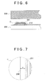
- the resist film 210 can be made less likely to peel away near the end portion. This will now be described with reference to FIGS. 6 to 8 .
- FIG. 6 is a view illustrating how a resist film is unlikely to peel away from the vicinity of a circuit conductor in a multilayer circuit board according to a modified example of this embodiment during a compression bonding process.
- FIG. 7 is a plan view showing a substrate end portion and a wiring conductor according to a modified example of this embodiment.
- FIG. 8 is a plan view showing a substrate end portion and a wiring conductor according to another modified example of this embodiment.
- an end portion position of the wiring conductor 201 that is closest to the end portion of the multilayer circuit board 200 is farther removed from the end portion of the multilayer circuit board 200 than the conventional position shown in FIG. 5 .
- the resist film 210 formed on the substrate end portion-side end portion of the wiring conductor 201 which is illustrated as a region surrounded by a dotted line C in FIG 6 , for example, is not excessively thin and does not have a distorted sectional shape.
- the reason for this is that the end portion of the multilayer circuit board 200 is comparatively removed from the end portion of the wiring conductor 201, and therefore, during application, the resist film 210 can be stretched gently while maintaining sufficient thickness.
- the resist film 210 is less likely to peel away.
- this distance or in other words a distance d between the end portion of the multilayer circuit board 200 and the end portion of the wiring conductor 201 shown in FIG. 7 , is preferably set at no less than at least 1 mm. In so doing, the resist film 210 can be stretched gently while maintaining sufficient thickness during application.
- the width of the wiring conductor 201 i.e. the length of a perpendicular direction to the direction in which the side of the substrate end portion extends along the substrate surface, is preferably as long as possible.
- the wiring conductor 201 is preferably formed from solid copper foil. The reason for this is that when the width of the wiring conductor 201 is small, the cross-section of the resist film 210 on the wiring conductor 201 takes a sharp curved shape, but when the width of the wiring conductor 201 is great, it is easy to stretch the resist film 210 gently while maintaining sufficient thickness.
- the resist film 210 is less likely to peel away.
- this width or in other words a width w of the solid copper foil forming the wiring conductor 201 shown in FIG. 8 , is preferably set at no less than at least 2 mm. In so doing, the resist film 210 can be stretched gently while maintaining sufficient thickness during application.
- a multilayer circuit board (100) serving as a motor driving circuit board is structured such that conductors of a first layer (110), a second layer (120), a third layer (130), and a fourth layer (140), which serve as conductor layers provided below an empty space to be occupied by a sealing material (170) when the sealing material (170) is charged onto a lower surface of a shunt resistor (12) serving as an electronic component having a large conductor surface, do not exist in a part facing the empty space.
- a shunt resistor (12) serving as an electronic component having a large conductor surface
Landscapes
- Engineering & Computer Science (AREA)
- Microelectronics & Electronic Packaging (AREA)
- Manufacturing & Machinery (AREA)
- Production Of Multi-Layered Print Wiring Board (AREA)
- Non-Metallic Protective Coatings For Printed Circuits (AREA)
Abstract
A multilayer circuit board (100) serving as a motor driving circuit board is structured such that conductors of a first layer (110), a second layer (120), a third layer (130), and a fourth layer (140), which serve as conductor layers provided below an empty space to be occupied by a sealing material (170) when the sealing material (170) is charged onto a lower surface of a shunt resistor (12) serving as an electronic component having a large conductor surface, do not exist in a part facing the empty space. With this structure, it is possible to ensure that a capacitor is not formed between the circuit board (100) and the shunt resistor (12) without the need for an inflow prevention tool.
As a result, an accurate current detection signal can be obtained reliably.
Description
- The invention relates to a multilayer circuit board and to a motor driving circuit board used in an electric power steering apparatus, employing the multilayer circuit board.
- An electric power steering apparatus for a vehicle drives a steering assist motor in accordance with a steering torque applied to a steering wheel by a driver, a vehicle speed, and so on, such that a favorable steering assist force is obtained. The steering assist motor is driven by a motor driving circuit built into an electronic control unit. When driving the steering assist motor, the motor driving circuit controls great power between approximately 500 and 2000 W. The electronic control unit will be referred to hereafter as an ECU.
- At this time, the motor driving circuit generates heat, and therefore, to prevent malfunctions and damage in the ECU caused by the generated heat, the motor driving circuit is packaged on a circuit board exhibiting favorable thermal conductivity. As shown in
FIG. 9A , for example, the motor driving circuit is packaged on a metallic circuit board constructed by forming onecopper conductor layer 91 and oneresin insulating layer 92 on an aluminum metallic substrate 93 (heat sink). - Electronic components can only be packaged on one side of the circuit board shown in
FIG. 9A . More specifically, electronic components can only be packaged on theconductor layer 91, and therefore a large area of the ECU is occupied by the circuit board. As one method of reducing the substrate area, the circuit board may be formed in multiple layers, as shown inFIG. 9B . A ceramic multilayer substrate shown inFIG. 9B is formed by laminating thecopper conductor layer 91 and a ceramicinsulating layer 94 in multiple layers and adhering the laminated layers to the aluminum metallic substrate 93 (heat sink) using an adhesive 95. By forming the circuit board from multiple layers in this manner, the substrate area can be reduced. - The following related art is available. International Patent Application 2008/078739 discloses a constitution for a multilayer circuit board in which an electronic component such as a power metal oxide semiconductor field effect transistor (MOSFET) is caused to radiate heat by forming a conductor layer on an inner surface using copper plating or the like and providing a heat dissipating via filled with a resin in the interior. Further, Japanese Patent Application Publication No.
2006-74014 JP-A-2006-74014 - Electronic components carried on a multilayer motor driving circuit board as described above include a semiconductor bear chip laid by wire bonding and a soldered current detecting shunt resistor. To protect these electronic components and wires, a normal substrate is sealed by an insulating resin material. At this time, the sealing insulating material (sealing material) may flow into a gap between the shunt resistor and the substrate. As a result, a capacitor may be formed on either side of the sealing material, which is a dielectric, causing disturbances during current detection.
- In a conventional method relating to this point, a component such as an inflow prevention tool may be newly attached to the periphery of the shunt resistor to prevent inflow of the sealing material, but due to the cost of the inflow prevention tool itself and the need for a process to attach the tool, the manufacturing cost of the substrate increases.
- It is therefore an object of the invention to provide a multilayer circuit board structured so that a capacitor such as that described above is not formed between the circuit board and a shunt resistor on either side of a sealing material even without attaching a new component such as a sealing material inflow prevention tool, and a motor driving circuit board for an electric power steering apparatus that employs the multilayer circuit board.
- A multilayer circuit board formed by laminating conductor layers and insulating layers alternately according to a first aspect of the invention includes: a conductor that has a surface substantially parallel to a top surface of the multilayer circuit board, and that is connected to an uppermost conductor layer such that a gap is formed between the conductor and the top surface of the multilayer circuit board; and a sealing material serving as a dielectric that is charged into a space including a periphery of the conductor and the gap, wherein, in the conductor layers, a conductor is not formed in a position facing the gap in a lamination direction of the conductor layers and the insulating layers.
- In the multilayer circuit board according to this aspect, the conductor layers do not include a conductor in the position facing the gap in the lamination direction of the conductor layers and insulating layers to ensure that a capacitor is not formed on either side of the sealing material serving as the dielectric that is charged into the space including the periphery of the conductor and the gap, i.e. between the substantially parallel surface of the conductor to the top surface of the multilayer circuit board and the conductor layers positioned opposite the conductor via the gap. In so doing, it is possible to ensure that a capacitor is not formed between the circuit board and the conductor on either side of the sealing material without attaching a new component such as an inflow prevention tool for preventing the sealing material from entering the gap.
- Further, in the multilayer circuit board according to the aspect described above, in at least one of the conductor layers, a part facing the gap in the lamination direction of the conductor layers and the insulating layers may be removed.
- According to this aspect, the part facing the gap in the lamination direction of the conductor layers and the insulating layers is removed from at least one of the conductor layers, and it is therefore possible to ensure that a capacitor is not formed between the conductor and the conductor layer on either side of the sealing material.
- A motor driving circuit board for an electric power steering apparatus, which is formed by laminating conductor layers and insulating layers alternately, according to a second aspect of the invention includes: a current detecting resistor that has a surface substantially parallel to a top surface of the motor driving circuit board, and that is connected to an uppermost conductor layer such that a gap is formed between the current detecting resistor and the top surface of the motor driving circuit board; and a sealing material serving as a dielectric that is charged into a space including a periphery of the resistor and the gap, wherein, in the conductor layers, a conductor is not formed in a part facing the gap in a lamination direction of the conductor layers and the insulating layers.
- According to the second aspect, the effects of the first aspect can be exhibited in a motor driving circuit board, and since the current detecting resistor, which is particularly likely to be affected when the sealing material forms a capacitor, is not affected in this manner, accurate current detection can be performed reliably.
- The features, advantages, and technical and industrial significance of this invention will be described in the following detailed description of example embodiments of the invention with reference to the accompanying drawings, in which like numerals denote like elements, and wherein:
-
FIG. 1 is a partial sectional view showing a multilayer circuit board according to an embodiment of the invention; -
FIG. 2 is a circuit diagram of the multilayer circuit board according to this embodiment; -
FIG. 3 is a partial exploded perspective view showing the structure of each layer of the multilayer circuit board according to this embodiment; -
FIG. 4 is a schematic sectional view and a schematic plan view of a multilayer circuit board formed with a resist film; -
FIG. 5 is a view illustrating how a resist film is likely to peel away from the vicinity of a circuit conductor in a multilayer circuit board according to the related art during a compression bonding process; -
FIG. 6 is a view illustrating how a resist film is unlikely to peel away from the vicinity of a circuit conductor in a multilayer circuit board according to a modified example of this embodiment during a compression bonding process; -
FIG. 7 is a plan view showing a substrate end portion and a wiring conductor according to a modified example of this embodiment; -
FIG. 8 is a plan view showing a substrate end portion and a wiring conductor according to another modified example of this embodiment; -
FIG. 9A is a sectional view showing a circuit board according to the related art; and -
FIG. 9B is a sectional view showing a circuit board according to the related art. - A multilayer circuit board according to this embodiment is a motor driving circuit board for an electric power steering apparatus, which is used when built into an ECU of the electric power steering apparatus.
- The ECU includes a motor control circuit that calculates an amount of a drive current supplied to a steering assist motor, and a motor driving circuit that drives the steering assist motor by controlling a large current. A current flowing through the motor control circuit when operative and an amount of heat generated thereby are both small, whereas a current flowing through the motor driving circuit when operative and an amount of heat generated thereby are both large. The motor driving circuit is packaged on a motor driving circuit board, and the motor control circuit is packaged on a separate circuit board. The structure of a multilayer circuit board serving as a motor driving circuit board will be described below with reference to
FIGS. 1 to 3 . -
FIG. 1 is a partial sectional view showing a multilayer circuit board according to an embodiment of the invention.FIG. 2 is a circuit diagram of the multilayer circuit board.FIG. 3 is a partial exploded perspective view showing the structure of each layer of the multilayer circuit board. - A
multilayer circuit board 100 shown in the drawings has a four-layer structure in which a first layer (top layer) 110, asecond layer 120, athird layer 130 and afourth layer 140, which serve as conductor layers, andinsulating layers 150 provided between the respective conductor layers are formed by thermal compression bonding. The conductor layer is formed from a highly conductive metal such as copper, and the insulating layer is formed from so-called pre-preg, which is a composite formed by impregnating glass fiber with an insulating resin material. Note that an aluminum metallic base, not shown in the drawings, is subjected to thermal compression bonding onto a lower surface of themultilayer circuit board 100 for the purpose of heat dissipation. - The top surface of the
multilayer circuit board 100 carries ashunt resistor 12, which is a current detection resistor, and sixMOSFETs FIG. 1 . Upper connection terminals of the MOSFETs are wire-bonded to wiring conductors formed from aluminum wires and provided in predetermined positions on thefirst layer 110. Theshunt resistor 12 is soldered to the wiring conductors provided in predetermined positions on thefirst layer 110 bysolder 105. - As shown in
FIG. 2 , drain terminals of the MOSFETs 10u, 10v, 10w are connected to a positive electrode of a power supply portion, not shown in the drawing, and source terminals thereof are connected to an input terminal of a corresponding motor phase. Source terminals of the MOSFETs 11u, 11v, 11w are connected to a negative electrode (ground electrode) of the power supply portion, not shown in the drawing, via theshunt resistor 12, and drain terminals thereof are connected to the input terminal of the corresponding motor phase. - To protect the electronic components, wires, and the like on the
multilayer circuit board 100, sealing is implemented over the entire substrate top surface using a sealingmaterial 170 made of an insulating resin. The sealingmaterial 170 is an insulating resin such as an epoxy resin, which is applied in a liquid state and then thermally hardened to protect the sealed electronic components and wires from physical impacts, moisture, and so on. Accordingly, the sealingmaterial 170 is applied to adhere tightly to the electronic components without gaps and charged into a gap (space) formed by a region surrounded by a lower surface of theshunt resistor 12, the two ends of which are soldered by thesolder 105, the top surface of themultilayer circuit board 100, and thesolder 105. - However, the sealing
material 170 has a predetermined dielectric constant, and therefore, when the sealingmaterial 170 is charged onto the lower surface of theshunt resistor 12, a large current flows into themultilayer circuit board 100. As a result, a capacitor may be formed between the lower surface of theshunt resistor 12, which serves as a conductor having a comparatively large surface area, and the conductor disposed therebelow, which has a comparatively large surface area. Theshunt resistor 12 is used for current detection, and therefore, if this capacitor is formed, a large problem arises in that irregularities occur in a current detection signal. - To solve this problem, in the
multilayer circuit board 100 according to this embodiment, the conductors of thefirst layer 110,second layer 120,third layer 130, andfourth layer 140, which serve as the conductor layers positioned below the space to be occupied by the sealingmaterial 170 when the sealingmaterial 170 is charged onto the lower surface of theshunt resistor 12, or in other words the empty space prior to charging of the sealingmaterial 170, do not exist in the parts facing the position of this empty space. This will now be described in detail with reference toFIG. 3 . -
FIG. 3 is a schematic exploded perspective view showing the shape of the conductor layers below the shunt resistor. As shown inFIG. 3 , a wiring conductor of thefirst layer 110 is disposed below theshunt resistor 12 in the vicinity of the two ends thereof via thesolder 105, not shown inFIG. 3 , in a lamination direction of the respective layers. Meanwhile, near the center of theshunt resistor 12, or in other words a part positioned below the empty space to be occupied by the sealingmaterial 170 prior to charging of the sealingmaterial 170 in the lamination direction of the respective layers, the wiring conductor of thefirst layer 110 does not exist. - A wiring conductor of the
second layer 120 functions here as a ground wire (GND wire), and even though thesecond layer 120 forms a solid copper foil region having a lowered normal resistance value in order to suppress noise, or in other words a wiring region having a large surface area, thesecond layer 120 is shaped such that the conductor is removed only from the part positioned below and facing the empty space in the lamination direction of the respective layers, whereby a hole is formed in the center of the wiring conductor of thesecond layer 120, as shown inFIG. 3 . This applies similarly to a wiring conductor forming a solid copper foil (solid wiring region) of thethird layer 130, which functions as a power supply wire. - Further, the wiring conductor of the
fourth layer 140 functions as a normal wire, and as shown inFIG. 3 , the conductor is removed only from the part positioned below and facing the empty space in the lamination direction of the respective layers such that the wiring conductor of thefourth layer 140 forms a partially cut-away notch. - By removing the wiring conductor from the part positioned directly below the empty space in the lamination direction of the respective layers as described above, it is possible to ensure that the capacitor that would be formed between the wiring conductor and the lower surface of the
shunt resistor 12 on either side of thedielectric sealing material 170 charged into the empty space if the wiring conductor existed in this part is not formed. - Note that the range of the parts of the
second layer 120 to thefourth layer 140 that are positioned directly below the empty space in the lamination direction of the respective layers does not have to match the region positioned directly below the empty space completely accurately, and may be formed wider than the range positioned directly below the empty space, in which the possibility of capacity formation exists. Moreover, if a capacitance value of the formed capacitor is small enough to pose no problems, the range positioned directly below the empty space can be reduced. - Further, the wiring conductors of the
second layer 120 to thefourth layer 140 are shaped such that only the parts thereof positioned directly below the empty space in the lamination direction of the respective layers are removed, but as long as the conductor does not exist in the part positioned directly below the empty space, the capacitor described above is not formed. It is therefore possible for all or a part of the wiring conductors of thesecond layer 120 to thefourth layer 140 in the vicinity of the part positioned directly below the empty space to be omitted from an original wiring design. For example, the wires forming thefourth layer 140 may all pass positions removed from the range positioned directly below the empty space. - Furthermore, the
multilayer circuit board 100 may be formed with a plurality of the current detectingshunt resistors 12, and theshunt resistor 12 may be replaced by another electronic component that may form the aforementioned capacitor, or in other words an electronic component that includes a conductor having a surface substantially parallel to the top surface of themultilayer circuit board 100. - As described above, the
multilayer circuit board 100 serving as a motor driving circuit board is structured such that the conductors of thesecond layer 120,third layer 130, andfourth layer 140, which serve as the conductor layers provided below the space (empty space) to be occupied by the sealingmaterial 170 when charged onto the lower surface of theshunt resistor 12, do not exist in the part facing this empty space. With this structure, it is possible to ensure that the capacitor described above is not formed between the conductor and theshunt resistor 12 without attaching a new component such as an inflow prevention tool for preventing the sealingmaterial 170 from entering the empty space. Moreover, the capacitor is not formed regardless of the manner in which the sealingmaterial 170 is charged into the empty space, and therefore an accurate current detection signal can be obtained reliably. - A circuit board having a normal metallic base is used as a circuit board for controlling a current exceeding several tens of amperes, for example, such as the
multilayer circuit board 100 described above, which is a motor driving circuit board used in an electric power steering apparatus. This type of circuit board requires a process for compression-bonding the metallic base to a printed board, but in this process, a resist film formed on the top surface of the printed board to protect the circuit may partially peel away. In particular, when the metallic base is compression-bonded to a multilayer circuit board, the multilayer circuit board is thick and the pressure required for the compression bonding is great, and therefore the resist film is particularly likely to peel away. This peeling of the resist film will now be described in detail with reference toFIGS. 4 and 5 . -
FIG. 4 is a schematic sectional view and a schematic plan view of a multilayer circuit board formed with a resist film, andFIG. 5 is a view illustrating how a resist film is likely to peel away from the vicinity of a circuit conductor in a multilayer circuit board during a compression bonding process. - As shown in
FIG. 4 , a resistfilm 210 functioning as solder resist is formed on amultilayer circuit board 200. The resistfilm 210 is applied to themultilayer circuit board 200 using a well-known method such as a spraying method or a curtain method, and then hardened. When a metallic base made of aluminum or the like is compression-bonded to themultilayer circuit board 200 using a thermal compression bonding apparatus or the like, the resist film is particularly likely to peel away from end portions of the substrate, i.e. regions surrounded by dotted lines E inFIG. 4 , for example. A possible reason for this is that in the vicinity of the end portions of the wiring conductors provided near the substrate end portions, the thickness of the resist film is more likely to decrease and the resist film is more likely to take a distorted sectional shape including a projecting portion. - More specifically, as shown in
FIG. 5 , the resistfilm 210 is formed on awiring conductor 201 provided near an end portion of themultilayer circuit board 200, but the resistfilm 210 formed on a substrate end portion-side end portion of thewiring conductor 201 is particularly thin and has a distorted sectional shape, as shown by the region surrounded by a dotted line B inFIG. 5 , for example. A possible reason for this is that the end portion of themultilayer circuit board 200 is close to the end portion of thewiring conductor 201, and therefore, during application, the resistfilm 210 cannot be stretched gently while maintaining sufficient thickness. Here, the metallic base, not shown in the drawings, is thermal compression-bonded to the lower surface of themultilayer circuit board 200, and therefore, when pressure is applied to themultilayer circuit board 200 by a pressingupper plate 300 of the thermal compression bonding apparatus from the upper side of the drawing toward the lower side of the drawing, stress concentrates in the part of the resistfilm 210 having the sectional shape described above. As a result, the resistfilm 210 may peel away. - By increasing the distance between the end portion of the
multilayer circuit board 200 and the end portion of thewiring conductor 201 so that the resistfilm 210 stretches gently while maintaining sufficient thickness, the resistfilm 210 can be made less likely to peel away near the end portion. This will now be described with reference toFIGS. 6 to 8 . -
FIG. 6 is a view illustrating how a resist film is unlikely to peel away from the vicinity of a circuit conductor in a multilayer circuit board according to a modified example of this embodiment during a compression bonding process.FIG. 7 is a plan view showing a substrate end portion and a wiring conductor according to a modified example of this embodiment.FIG. 8 is a plan view showing a substrate end portion and a wiring conductor according to another modified example of this embodiment. - As shown in
FIG. 6 , an end portion position of thewiring conductor 201 that is closest to the end portion of themultilayer circuit board 200 is farther removed from the end portion of themultilayer circuit board 200 than the conventional position shown inFIG. 5 . Hence, the resistfilm 210 formed on the substrate end portion-side end portion of thewiring conductor 201, which is illustrated as a region surrounded by a dotted line C inFIG 6 , for example, is not excessively thin and does not have a distorted sectional shape. The reason for this is that the end portion of themultilayer circuit board 200 is comparatively removed from the end portion of thewiring conductor 201, and therefore, during application, the resistfilm 210 can be stretched gently while maintaining sufficient thickness. - Thus, the resist
film 210 is less likely to peel away. However, when a resist material having a typical composition is used, this distance, or in other words a distance d between the end portion of themultilayer circuit board 200 and the end portion of thewiring conductor 201 shown inFIG. 7 , is preferably set at no less than at least 1 mm. In so doing, the resistfilm 210 can be stretched gently while maintaining sufficient thickness during application. - Further, the width of the
wiring conductor 201, i.e. the length of a perpendicular direction to the direction in which the side of the substrate end portion extends along the substrate surface, is preferably as long as possible. In other words, thewiring conductor 201 is preferably formed from solid copper foil. The reason for this is that when the width of thewiring conductor 201 is small, the cross-section of the resistfilm 210 on thewiring conductor 201 takes a sharp curved shape, but when the width of thewiring conductor 201 is great, it is easy to stretch the resistfilm 210 gently while maintaining sufficient thickness. - Thus, the resist
film 210 is less likely to peel away. However, when a resist material having a typical composition is used, this width, or in other words a width w of the solid copper foil forming thewiring conductor 201 shown inFIG. 8 , is preferably set at no less than at least 2 mm. In so doing, the resistfilm 210 can be stretched gently while maintaining sufficient thickness during application.
A multilayer circuit board (100) serving as a motor driving circuit board is structured such that conductors of a first layer (110), a second layer (120), a third layer (130), and a fourth layer (140), which serve as conductor layers provided below an empty space to be occupied by a sealing material (170) when the sealing material (170) is charged onto a lower surface of a shunt resistor (12) serving as an electronic component having a large conductor surface, do not exist in a part facing the empty space. With this structure, it is possible to ensure that a capacitor is not formed between the circuit board (100) and the shunt resistor (12) without the need for an inflow prevention tool. As a result, an accurate current detection signal can be obtained reliably.
Claims (8)
- A multilayer circuit board (100) formed by laminating conductor layers (110, 120, 130, 140) and insulating layers (150) alternately, characterized by comprising:a conductor (12) that has a surface substantially parallel to a top surface of the multilayer circuit board (100), and that is connected to an uppermost conductor layer (110) such that a gap is formed between the conductor (12) and the top surface of the multilayer circuit board (100); anda sealing material (170) serving as a dielectric that is charged into a space including a periphery of the conductor (12) and the gap,wherein, in the conductor layers (110, 120, 130, 140), a conductor is not formed in a position facing the gap in a lamination direction of the conductor layers (110, 120, 130, 140) and the insulating layers (150).
- The multilayer circuit board (100) according to claim 1, wherein
in at least one of the conductor layers (110, 120, 130, 140), a part facing the gap in the lamination direction of the conductor layers (110, 120, 130, 140) and the insulating layers (150) is removed. - The multilayer circuit board (100) according to claim 2, wherein
in all of the conductor layers (110, 120, 130, 140), the part facing the gap in the lamination direction of the conductor layers (110, 120, 130, 140) and the insulating layers (150) is removed. - The multilayer circuit board (100) according to claims 2 or 3, wherein
the part of the conductor layer (110, 120, 130, 140) is removed to form a hole in the conductor layer (110, 120, 130, 140). - The multilayer circuit board (100) according to claims 2 or 3, wherein
the part of the conductor layer (110, 120, 130, 140) is removed to form a notch in the conductor layer (110, 120, 130, 140). - The multilayer circuit board (100) according to any one of claims 1 to 5, wherein
the conductor (12) is connected to the uppermost conductor layer (110) via solder (105), and
the gap is formed in a region surrounded by the conductor (12), the solder (105), and the top surface of the multilayer circuit board (100). - The multilayer circuit board (100) according to any one of claims 1 to 6, wherein
the conductor (12) is a current detecting resistor. - A motor driving circuit board (100) for an electric power steering apparatus, which is formed by laminating conductor layers (110, 120, 130, 140) and insulating layers (150) alternately, characterized by comprising:a current detecting resistor (12) that has a surface substantially parallel to a top surface of the motor driving circuit board (100), and that is connected to an uppermost conductor layer (110) such that a gap is formed between the current detecting resistor (12) and the top surface of the motor driving circuit board (100); anda sealing material (170) serving as a dielectric that is charged into a space including a periphery of the resistor (12) and the gap,wherein, in the conductor layers (110, 120, 130, 140), a conductor is not formed in a part facing the gap in a lamination direction of the conductor layers (110, 120, 130, 140) and the insulating layers (150).
Applications Claiming Priority (1)
| Application Number | Priority Date | Filing Date | Title |
|---|---|---|---|
| JP2008240246A JP5359146B2 (en) | 2008-09-19 | 2008-09-19 | Multilayer circuit board |
Publications (1)
| Publication Number | Publication Date |
|---|---|
| EP2166824A1 true EP2166824A1 (en) | 2010-03-24 |
Family
ID=41217732
Family Applications (1)
| Application Number | Title | Priority Date | Filing Date |
|---|---|---|---|
| EP09170571A Withdrawn EP2166824A1 (en) | 2008-09-19 | 2009-09-17 | Multilayer circuit board and motor driving circuit board |
Country Status (3)
| Country | Link |
|---|---|
| US (1) | US20100071947A1 (en) |
| EP (1) | EP2166824A1 (en) |
| JP (1) | JP5359146B2 (en) |
Families Citing this family (2)
| Publication number | Priority date | Publication date | Assignee | Title |
|---|---|---|---|---|
| US9885743B2 (en) * | 2012-12-17 | 2018-02-06 | Itron, Inc. | Electric meter base level printed circuit board |
| US9983233B2 (en) * | 2014-02-06 | 2018-05-29 | Texas Instruments Incorporated | Current sensor |
Citations (4)
| Publication number | Priority date | Publication date | Assignee | Title |
|---|---|---|---|---|
| US6078155A (en) * | 1999-01-18 | 2000-06-20 | Mitsubishi Denki Kabushiki Kaisha | Electric power steering circuit assembly |
| US20030107056A1 (en) * | 2001-12-08 | 2003-06-12 | National Semiconductor Corporation | Substrate pads with reduced impedance mismatch and methods to fabricate substrate pads |
| JP2006074014A (en) | 2004-08-06 | 2006-03-16 | Toyota Industries Corp | Multilayer printed board, and method for controlling impedance of microstrip line |
| US20080093113A1 (en) * | 2006-10-20 | 2008-04-24 | Industrial Technology Research Institute | Complementary mirror image embedded planar resistor architecture |
Family Cites Families (7)
| Publication number | Priority date | Publication date | Assignee | Title |
|---|---|---|---|---|
| JPH07106507A (en) * | 1993-10-05 | 1995-04-21 | Mitsubishi Electric Corp | Hybrid integrated circuit device |
| JP2002141672A (en) * | 2000-11-02 | 2002-05-17 | Hitachi Ltd | Multilayer printed wiring board, manufacturing method thereof, mounting board, and electronic device |
| JP2003273525A (en) * | 2002-03-15 | 2003-09-26 | Kyocera Corp | Wiring board |
| JP4357817B2 (en) * | 2002-09-12 | 2009-11-04 | パナソニック株式会社 | Module with built-in circuit components |
| JP4350366B2 (en) * | 2002-12-24 | 2009-10-21 | パナソニック株式会社 | Electronic component built-in module |
| US7701728B2 (en) * | 2004-10-28 | 2010-04-20 | Kyocera Corporation | Electronic component module and radio comunications equipment |
| JP4730313B2 (en) * | 2007-01-24 | 2011-07-20 | ミツミ電機株式会社 | High frequency tuner module and tuner module |
-
2008
- 2008-09-19 JP JP2008240246A patent/JP5359146B2/en not_active Expired - Fee Related
-
2009
- 2009-09-08 US US12/585,204 patent/US20100071947A1/en not_active Abandoned
- 2009-09-17 EP EP09170571A patent/EP2166824A1/en not_active Withdrawn
Patent Citations (4)
| Publication number | Priority date | Publication date | Assignee | Title |
|---|---|---|---|---|
| US6078155A (en) * | 1999-01-18 | 2000-06-20 | Mitsubishi Denki Kabushiki Kaisha | Electric power steering circuit assembly |
| US20030107056A1 (en) * | 2001-12-08 | 2003-06-12 | National Semiconductor Corporation | Substrate pads with reduced impedance mismatch and methods to fabricate substrate pads |
| JP2006074014A (en) | 2004-08-06 | 2006-03-16 | Toyota Industries Corp | Multilayer printed board, and method for controlling impedance of microstrip line |
| US20080093113A1 (en) * | 2006-10-20 | 2008-04-24 | Industrial Technology Research Institute | Complementary mirror image embedded planar resistor architecture |
Also Published As
| Publication number | Publication date |
|---|---|
| JP5359146B2 (en) | 2013-12-04 |
| JP2010073911A (en) | 2010-04-02 |
| US20100071947A1 (en) | 2010-03-25 |
Similar Documents
| Publication | Publication Date | Title |
|---|---|---|
| US8288658B2 (en) | Multilayer circuit board and motor drive circuit board | |
| US7304370B2 (en) | Electronic device having wiring substrate and lead frame | |
| US8415565B2 (en) | Multilayer circuit substrate | |
| US9681558B2 (en) | Module with integrated power electronic circuitry and logic circuitry | |
| US7679914B2 (en) | Electronic controller | |
| US7903417B2 (en) | Electrical circuit assembly for high-power electronics | |
| JP7088132B2 (en) | Semiconductor devices and electronic devices | |
| US9978719B2 (en) | Electronic component, arrangement and method | |
| US20170358516A1 (en) | Power module | |
| WO2007026944A1 (en) | Circuit device and method for manufacturing same | |
| JP2007281452A (en) | Connection device for electronic components | |
| JP2008187146A (en) | Circuit equipment | |
| WO2010001505A1 (en) | Electronic component | |
| US20100071947A1 (en) | Multilayer circuit board and motor driving circuit board | |
| US6101098A (en) | Structure and method for mounting an electric part | |
| JP3544757B2 (en) | Semiconductor device and manufacturing method thereof | |
| US7907390B2 (en) | Circuit device | |
| JP4527292B2 (en) | Semiconductor power module | |
| WO2008045430A1 (en) | Electrical circuit assembly for high-power electronics | |
| CN222356697U (en) | Ultra-thin controller integrating direct-current motor drive and three-phase motor drive | |
| JP2004273788A (en) | Electronic device manufacturing method | |
| CN101436588A (en) | Circuit module | |
| JPH065697B2 (en) | Printed wiring board for mounting semiconductor chips | |
| JPH0789575B2 (en) | Printed wiring board for mounting semiconductor chips | |
| JPH0945850A (en) | Hybrid integrated circuit device |
Legal Events
| Date | Code | Title | Description |
|---|---|---|---|
| PUAI | Public reference made under article 153(3) epc to a published international application that has entered the european phase |
Free format text: ORIGINAL CODE: 0009012 |
|
| AK | Designated contracting states |
Kind code of ref document: A1 Designated state(s): AT BE BG CH CY CZ DE DK EE ES FI FR GB GR HR HU IE IS IT LI LT LU LV MC MK MT NL NO PL PT RO SE SI SK SM TR |
|
| AX | Request for extension of the european patent |
Extension state: AL BA RS |
|
| STAA | Information on the status of an ep patent application or granted ep patent |
Free format text: STATUS: THE APPLICATION IS DEEMED TO BE WITHDRAWN |
|
| 18D | Application deemed to be withdrawn |
Effective date: 20100925 |