JP2007281452A - Electronic component connection device - Google Patents
Electronic component connection device Download PDFInfo
- Publication number
- JP2007281452A JP2007281452A JP2007070666A JP2007070666A JP2007281452A JP 2007281452 A JP2007281452 A JP 2007281452A JP 2007070666 A JP2007070666 A JP 2007070666A JP 2007070666 A JP2007070666 A JP 2007070666A JP 2007281452 A JP2007281452 A JP 2007281452A
- Authority
- JP
- Japan
- Prior art keywords
- film
- connection device
- connection
- conductive
- layer
- Prior art date
- Legal status (The legal status is an assumption and is not a legal conclusion. Google has not performed a legal analysis and makes no representation as to the accuracy of the status listed.)
- Pending
Links
Images

Classifications
-
- H—ELECTRICITY
- H05—ELECTRIC TECHNIQUES NOT OTHERWISE PROVIDED FOR
- H05K—PRINTED CIRCUITS; CASINGS OR CONSTRUCTIONAL DETAILS OF ELECTRIC APPARATUS; MANUFACTURE OF ASSEMBLAGES OF ELECTRICAL COMPONENTS
- H05K1/00—Printed circuits
- H05K1/02—Details
- H05K1/14—Structural association of two or more printed circuits
- H05K1/147—Structural association of two or more printed circuits at least one of the printed circuits being bent or folded, e.g. by using a flexible printed circuit
-
- H—ELECTRICITY
- H01—ELECTRIC ELEMENTS
- H01L—SEMICONDUCTOR DEVICES NOT COVERED BY CLASS H10
- H01L27/00—Devices consisting of a plurality of semiconductor or other solid-state components formed in or on a common substrate
- H01L27/02—Devices consisting of a plurality of semiconductor or other solid-state components formed in or on a common substrate including semiconductor components specially adapted for rectifying, oscillating, amplifying or switching and having at least one potential-jump barrier or surface barrier; including integrated passive circuit elements with at least one potential-jump barrier or surface barrier
-
- H—ELECTRICITY
- H01—ELECTRIC ELEMENTS
- H01L—SEMICONDUCTOR DEVICES NOT COVERED BY CLASS H10
- H01L23/00—Details of semiconductor or other solid state devices
- H01L23/12—Mountings, e.g. non-detachable insulating substrates
-
- H—ELECTRICITY
- H01—ELECTRIC ELEMENTS
- H01L—SEMICONDUCTOR DEVICES NOT COVERED BY CLASS H10
- H01L23/00—Details of semiconductor or other solid state devices
- H01L23/48—Arrangements for conducting electric current to or from the solid state body in operation, e.g. leads, terminal arrangements ; Selection of materials therefor
- H01L23/488—Arrangements for conducting electric current to or from the solid state body in operation, e.g. leads, terminal arrangements ; Selection of materials therefor consisting of soldered or bonded constructions
- H01L23/498—Leads, i.e. metallisations or lead-frames on insulating substrates, e.g. chip carriers
- H01L23/49822—Multilayer substrates
-
- H—ELECTRICITY
- H01—ELECTRIC ELEMENTS
- H01L—SEMICONDUCTOR DEVICES NOT COVERED BY CLASS H10
- H01L23/00—Details of semiconductor or other solid state devices
- H01L23/48—Arrangements for conducting electric current to or from the solid state body in operation, e.g. leads, terminal arrangements ; Selection of materials therefor
- H01L23/488—Arrangements for conducting electric current to or from the solid state body in operation, e.g. leads, terminal arrangements ; Selection of materials therefor consisting of soldered or bonded constructions
- H01L23/498—Leads, i.e. metallisations or lead-frames on insulating substrates, e.g. chip carriers
- H01L23/4985—Flexible insulating substrates
-
- H—ELECTRICITY
- H01—ELECTRIC ELEMENTS
- H01L—SEMICONDUCTOR DEVICES NOT COVERED BY CLASS H10
- H01L24/00—Arrangements for connecting or disconnecting semiconductor or solid-state bodies; Methods or apparatus related thereto
- H01L24/01—Means for bonding being attached to, or being formed on, the surface to be connected, e.g. chip-to-package, die-attach, "first-level" interconnects; Manufacturing methods related thereto
- H01L24/18—High density interconnect [HDI] connectors; Manufacturing methods related thereto
- H01L24/23—Structure, shape, material or disposition of the high density interconnect connectors after the connecting process
- H01L24/24—Structure, shape, material or disposition of the high density interconnect connectors after the connecting process of an individual high density interconnect connector
-
- H—ELECTRICITY
- H01—ELECTRIC ELEMENTS
- H01L—SEMICONDUCTOR DEVICES NOT COVERED BY CLASS H10
- H01L24/00—Arrangements for connecting or disconnecting semiconductor or solid-state bodies; Methods or apparatus related thereto
- H01L24/80—Methods for connecting semiconductor or other solid state bodies using means for bonding being attached to, or being formed on, the surface to be connected
- H01L24/82—Methods for connecting semiconductor or other solid state bodies using means for bonding being attached to, or being formed on, the surface to be connected by forming build-up interconnects at chip-level, e.g. for high density interconnects [HDI]
-
- H—ELECTRICITY
- H05—ELECTRIC TECHNIQUES NOT OTHERWISE PROVIDED FOR
- H05K—PRINTED CIRCUITS; CASINGS OR CONSTRUCTIONAL DETAILS OF ELECTRIC APPARATUS; MANUFACTURE OF ASSEMBLAGES OF ELECTRICAL COMPONENTS
- H05K3/00—Apparatus or processes for manufacturing printed circuits
- H05K3/30—Assembling printed circuits with electric components, e.g. with resistor
- H05K3/32—Assembling printed circuits with electric components, e.g. with resistor electrically connecting electric components or wires to printed circuits
- H05K3/328—Assembling printed circuits with electric components, e.g. with resistor electrically connecting electric components or wires to printed circuits by welding
-
- H—ELECTRICITY
- H01—ELECTRIC ELEMENTS
- H01L—SEMICONDUCTOR DEVICES NOT COVERED BY CLASS H10
- H01L2224/00—Indexing scheme for arrangements for connecting or disconnecting semiconductor or solid-state bodies and methods related thereto as covered by H01L24/00
- H01L2224/01—Means for bonding being attached to, or being formed on, the surface to be connected, e.g. chip-to-package, die-attach, "first-level" interconnects; Manufacturing methods related thereto
- H01L2224/02—Bonding areas; Manufacturing methods related thereto
- H01L2224/04—Structure, shape, material or disposition of the bonding areas prior to the connecting process
- H01L2224/05—Structure, shape, material or disposition of the bonding areas prior to the connecting process of an individual bonding area
- H01L2224/0554—External layer
- H01L2224/0555—Shape
- H01L2224/05552—Shape in top view
- H01L2224/05554—Shape in top view being square
-
- H—ELECTRICITY
- H01—ELECTRIC ELEMENTS
- H01L—SEMICONDUCTOR DEVICES NOT COVERED BY CLASS H10
- H01L2224/00—Indexing scheme for arrangements for connecting or disconnecting semiconductor or solid-state bodies and methods related thereto as covered by H01L24/00
- H01L2224/01—Means for bonding being attached to, or being formed on, the surface to be connected, e.g. chip-to-package, die-attach, "first-level" interconnects; Manufacturing methods related thereto
- H01L2224/18—High density interconnect [HDI] connectors; Manufacturing methods related thereto
- H01L2224/23—Structure, shape, material or disposition of the high density interconnect connectors after the connecting process
- H01L2224/24—Structure, shape, material or disposition of the high density interconnect connectors after the connecting process of an individual high density interconnect connector
- H01L2224/2401—Structure
- H01L2224/2402—Laminated, e.g. MCM-L type
-
- H—ELECTRICITY
- H01—ELECTRIC ELEMENTS
- H01L—SEMICONDUCTOR DEVICES NOT COVERED BY CLASS H10
- H01L2224/00—Indexing scheme for arrangements for connecting or disconnecting semiconductor or solid-state bodies and methods related thereto as covered by H01L24/00
- H01L2224/01—Means for bonding being attached to, or being formed on, the surface to be connected, e.g. chip-to-package, die-attach, "first-level" interconnects; Manufacturing methods related thereto
- H01L2224/26—Layer connectors, e.g. plate connectors, solder or adhesive layers; Manufacturing methods related thereto
- H01L2224/31—Structure, shape, material or disposition of the layer connectors after the connecting process
- H01L2224/32—Structure, shape, material or disposition of the layer connectors after the connecting process of an individual layer connector
- H01L2224/321—Disposition
- H01L2224/32151—Disposition the layer connector connecting between a semiconductor or solid-state body and an item not being a semiconductor or solid-state body, e.g. chip-to-substrate, chip-to-passive
- H01L2224/32221—Disposition the layer connector connecting between a semiconductor or solid-state body and an item not being a semiconductor or solid-state body, e.g. chip-to-substrate, chip-to-passive the body and the item being stacked
- H01L2224/32225—Disposition the layer connector connecting between a semiconductor or solid-state body and an item not being a semiconductor or solid-state body, e.g. chip-to-substrate, chip-to-passive the body and the item being stacked the item being non-metallic, e.g. insulating substrate with or without metallisation
-
- H—ELECTRICITY
- H01—ELECTRIC ELEMENTS
- H01L—SEMICONDUCTOR DEVICES NOT COVERED BY CLASS H10
- H01L2224/00—Indexing scheme for arrangements for connecting or disconnecting semiconductor or solid-state bodies and methods related thereto as covered by H01L24/00
- H01L2224/01—Means for bonding being attached to, or being formed on, the surface to be connected, e.g. chip-to-package, die-attach, "first-level" interconnects; Manufacturing methods related thereto
- H01L2224/42—Wire connectors; Manufacturing methods related thereto
- H01L2224/47—Structure, shape, material or disposition of the wire connectors after the connecting process
- H01L2224/48—Structure, shape, material or disposition of the wire connectors after the connecting process of an individual wire connector
- H01L2224/4805—Shape
- H01L2224/4809—Loop shape
- H01L2224/48091—Arched
-
- H—ELECTRICITY
- H01—ELECTRIC ELEMENTS
- H01L—SEMICONDUCTOR DEVICES NOT COVERED BY CLASS H10
- H01L2224/00—Indexing scheme for arrangements for connecting or disconnecting semiconductor or solid-state bodies and methods related thereto as covered by H01L24/00
- H01L2224/01—Means for bonding being attached to, or being formed on, the surface to be connected, e.g. chip-to-package, die-attach, "first-level" interconnects; Manufacturing methods related thereto
- H01L2224/42—Wire connectors; Manufacturing methods related thereto
- H01L2224/47—Structure, shape, material or disposition of the wire connectors after the connecting process
- H01L2224/48—Structure, shape, material or disposition of the wire connectors after the connecting process of an individual wire connector
- H01L2224/481—Disposition
- H01L2224/48151—Connecting between a semiconductor or solid-state body and an item not being a semiconductor or solid-state body, e.g. chip-to-substrate, chip-to-passive
- H01L2224/48221—Connecting between a semiconductor or solid-state body and an item not being a semiconductor or solid-state body, e.g. chip-to-substrate, chip-to-passive the body and the item being stacked
- H01L2224/48225—Connecting between a semiconductor or solid-state body and an item not being a semiconductor or solid-state body, e.g. chip-to-substrate, chip-to-passive the body and the item being stacked the item being non-metallic, e.g. insulating substrate with or without metallisation
- H01L2224/48227—Connecting between a semiconductor or solid-state body and an item not being a semiconductor or solid-state body, e.g. chip-to-substrate, chip-to-passive the body and the item being stacked the item being non-metallic, e.g. insulating substrate with or without metallisation connecting the wire to a bond pad of the item
-
- H—ELECTRICITY
- H01—ELECTRIC ELEMENTS
- H01L—SEMICONDUCTOR DEVICES NOT COVERED BY CLASS H10
- H01L2224/00—Indexing scheme for arrangements for connecting or disconnecting semiconductor or solid-state bodies and methods related thereto as covered by H01L24/00
- H01L2224/01—Means for bonding being attached to, or being formed on, the surface to be connected, e.g. chip-to-package, die-attach, "first-level" interconnects; Manufacturing methods related thereto
- H01L2224/42—Wire connectors; Manufacturing methods related thereto
- H01L2224/47—Structure, shape, material or disposition of the wire connectors after the connecting process
- H01L2224/48—Structure, shape, material or disposition of the wire connectors after the connecting process of an individual wire connector
- H01L2224/484—Connecting portions
- H01L2224/4847—Connecting portions the connecting portion on the bonding area of the semiconductor or solid-state body being a wedge bond
- H01L2224/48472—Connecting portions the connecting portion on the bonding area of the semiconductor or solid-state body being a wedge bond the other connecting portion not on the bonding area also being a wedge bond, i.e. wedge-to-wedge
-
- H—ELECTRICITY
- H01—ELECTRIC ELEMENTS
- H01L—SEMICONDUCTOR DEVICES NOT COVERED BY CLASS H10
- H01L2224/00—Indexing scheme for arrangements for connecting or disconnecting semiconductor or solid-state bodies and methods related thereto as covered by H01L24/00
- H01L2224/01—Means for bonding being attached to, or being formed on, the surface to be connected, e.g. chip-to-package, die-attach, "first-level" interconnects; Manufacturing methods related thereto
- H01L2224/42—Wire connectors; Manufacturing methods related thereto
- H01L2224/47—Structure, shape, material or disposition of the wire connectors after the connecting process
- H01L2224/49—Structure, shape, material or disposition of the wire connectors after the connecting process of a plurality of wire connectors
- H01L2224/491—Disposition
- H01L2224/4912—Layout
- H01L2224/49175—Parallel arrangements
-
- H—ELECTRICITY
- H01—ELECTRIC ELEMENTS
- H01L—SEMICONDUCTOR DEVICES NOT COVERED BY CLASS H10
- H01L2224/00—Indexing scheme for arrangements for connecting or disconnecting semiconductor or solid-state bodies and methods related thereto as covered by H01L24/00
- H01L2224/73—Means for bonding being of different types provided for in two or more of groups H01L2224/10, H01L2224/18, H01L2224/26, H01L2224/34, H01L2224/42, H01L2224/50, H01L2224/63, H01L2224/71
- H01L2224/732—Location after the connecting process
- H01L2224/73251—Location after the connecting process on different surfaces
- H01L2224/73265—Layer and wire connectors
-
- H—ELECTRICITY
- H01—ELECTRIC ELEMENTS
- H01L—SEMICONDUCTOR DEVICES NOT COVERED BY CLASS H10
- H01L2224/00—Indexing scheme for arrangements for connecting or disconnecting semiconductor or solid-state bodies and methods related thereto as covered by H01L24/00
- H01L2224/80—Methods for connecting semiconductor or other solid state bodies using means for bonding being attached to, or being formed on, the surface to be connected
- H01L2224/85—Methods for connecting semiconductor or other solid state bodies using means for bonding being attached to, or being formed on, the surface to be connected using a wire connector
- H01L2224/8538—Bonding interfaces outside the semiconductor or solid-state body
- H01L2224/85399—Material
- H01L2224/854—Material with a principal constituent of the material being a metal or a metalloid, e.g. boron (B), silicon (Si), germanium (Ge), arsenic (As), antimony (Sb), tellurium (Te) and polonium (Po), and alloys thereof
- H01L2224/85438—Material with a principal constituent of the material being a metal or a metalloid, e.g. boron (B), silicon (Si), germanium (Ge), arsenic (As), antimony (Sb), tellurium (Te) and polonium (Po), and alloys thereof the principal constituent melting at a temperature of greater than or equal to 950°C and less than 1550°C
- H01L2224/85444—Gold (Au) as principal constituent
-
- H—ELECTRICITY
- H01—ELECTRIC ELEMENTS
- H01L—SEMICONDUCTOR DEVICES NOT COVERED BY CLASS H10
- H01L24/00—Arrangements for connecting or disconnecting semiconductor or solid-state bodies; Methods or apparatus related thereto
- H01L24/01—Means for bonding being attached to, or being formed on, the surface to be connected, e.g. chip-to-package, die-attach, "first-level" interconnects; Manufacturing methods related thereto
- H01L24/26—Layer connectors, e.g. plate connectors, solder or adhesive layers; Manufacturing methods related thereto
- H01L24/28—Structure, shape, material or disposition of the layer connectors prior to the connecting process
- H01L24/29—Structure, shape, material or disposition of the layer connectors prior to the connecting process of an individual layer connector
-
- H—ELECTRICITY
- H01—ELECTRIC ELEMENTS
- H01L—SEMICONDUCTOR DEVICES NOT COVERED BY CLASS H10
- H01L24/00—Arrangements for connecting or disconnecting semiconductor or solid-state bodies; Methods or apparatus related thereto
- H01L24/01—Means for bonding being attached to, or being formed on, the surface to be connected, e.g. chip-to-package, die-attach, "first-level" interconnects; Manufacturing methods related thereto
- H01L24/42—Wire connectors; Manufacturing methods related thereto
- H01L24/47—Structure, shape, material or disposition of the wire connectors after the connecting process
- H01L24/48—Structure, shape, material or disposition of the wire connectors after the connecting process of an individual wire connector
-
- H—ELECTRICITY
- H01—ELECTRIC ELEMENTS
- H01L—SEMICONDUCTOR DEVICES NOT COVERED BY CLASS H10
- H01L24/00—Arrangements for connecting or disconnecting semiconductor or solid-state bodies; Methods or apparatus related thereto
- H01L24/01—Means for bonding being attached to, or being formed on, the surface to be connected, e.g. chip-to-package, die-attach, "first-level" interconnects; Manufacturing methods related thereto
- H01L24/42—Wire connectors; Manufacturing methods related thereto
- H01L24/47—Structure, shape, material or disposition of the wire connectors after the connecting process
- H01L24/49—Structure, shape, material or disposition of the wire connectors after the connecting process of a plurality of wire connectors
-
- H—ELECTRICITY
- H01—ELECTRIC ELEMENTS
- H01L—SEMICONDUCTOR DEVICES NOT COVERED BY CLASS H10
- H01L2924/00—Indexing scheme for arrangements or methods for connecting or disconnecting semiconductor or solid-state bodies as covered by H01L24/00
- H01L2924/0001—Technical content checked by a classifier
- H01L2924/00014—Technical content checked by a classifier the subject-matter covered by the group, the symbol of which is combined with the symbol of this group, being disclosed without further technical details
-
- H—ELECTRICITY
- H01—ELECTRIC ELEMENTS
- H01L—SEMICONDUCTOR DEVICES NOT COVERED BY CLASS H10
- H01L2924/00—Indexing scheme for arrangements or methods for connecting or disconnecting semiconductor or solid-state bodies as covered by H01L24/00
- H01L2924/01—Chemical elements
- H01L2924/01005—Boron [B]
-
- H—ELECTRICITY
- H01—ELECTRIC ELEMENTS
- H01L—SEMICONDUCTOR DEVICES NOT COVERED BY CLASS H10
- H01L2924/00—Indexing scheme for arrangements or methods for connecting or disconnecting semiconductor or solid-state bodies as covered by H01L24/00
- H01L2924/01—Chemical elements
- H01L2924/01006—Carbon [C]
-
- H—ELECTRICITY
- H01—ELECTRIC ELEMENTS
- H01L—SEMICONDUCTOR DEVICES NOT COVERED BY CLASS H10
- H01L2924/00—Indexing scheme for arrangements or methods for connecting or disconnecting semiconductor or solid-state bodies as covered by H01L24/00
- H01L2924/01—Chemical elements
- H01L2924/01013—Aluminum [Al]
-
- H—ELECTRICITY
- H01—ELECTRIC ELEMENTS
- H01L—SEMICONDUCTOR DEVICES NOT COVERED BY CLASS H10
- H01L2924/00—Indexing scheme for arrangements or methods for connecting or disconnecting semiconductor or solid-state bodies as covered by H01L24/00
- H01L2924/01—Chemical elements
- H01L2924/01015—Phosphorus [P]
-
- H—ELECTRICITY
- H01—ELECTRIC ELEMENTS
- H01L—SEMICONDUCTOR DEVICES NOT COVERED BY CLASS H10
- H01L2924/00—Indexing scheme for arrangements or methods for connecting or disconnecting semiconductor or solid-state bodies as covered by H01L24/00
- H01L2924/01—Chemical elements
- H01L2924/01029—Copper [Cu]
-
- H—ELECTRICITY
- H01—ELECTRIC ELEMENTS
- H01L—SEMICONDUCTOR DEVICES NOT COVERED BY CLASS H10
- H01L2924/00—Indexing scheme for arrangements or methods for connecting or disconnecting semiconductor or solid-state bodies as covered by H01L24/00
- H01L2924/01—Chemical elements
- H01L2924/01033—Arsenic [As]
-
- H—ELECTRICITY
- H01—ELECTRIC ELEMENTS
- H01L—SEMICONDUCTOR DEVICES NOT COVERED BY CLASS H10
- H01L2924/00—Indexing scheme for arrangements or methods for connecting or disconnecting semiconductor or solid-state bodies as covered by H01L24/00
- H01L2924/01—Chemical elements
- H01L2924/01078—Platinum [Pt]
-
- H—ELECTRICITY
- H01—ELECTRIC ELEMENTS
- H01L—SEMICONDUCTOR DEVICES NOT COVERED BY CLASS H10
- H01L2924/00—Indexing scheme for arrangements or methods for connecting or disconnecting semiconductor or solid-state bodies as covered by H01L24/00
- H01L2924/01—Chemical elements
- H01L2924/01079—Gold [Au]
-
- H—ELECTRICITY
- H01—ELECTRIC ELEMENTS
- H01L—SEMICONDUCTOR DEVICES NOT COVERED BY CLASS H10
- H01L2924/00—Indexing scheme for arrangements or methods for connecting or disconnecting semiconductor or solid-state bodies as covered by H01L24/00
- H01L2924/01—Chemical elements
- H01L2924/01082—Lead [Pb]
-
- H—ELECTRICITY
- H01—ELECTRIC ELEMENTS
- H01L—SEMICONDUCTOR DEVICES NOT COVERED BY CLASS H10
- H01L2924/00—Indexing scheme for arrangements or methods for connecting or disconnecting semiconductor or solid-state bodies as covered by H01L24/00
- H01L2924/013—Alloys
- H01L2924/014—Solder alloys
-
- H—ELECTRICITY
- H01—ELECTRIC ELEMENTS
- H01L—SEMICONDUCTOR DEVICES NOT COVERED BY CLASS H10
- H01L2924/00—Indexing scheme for arrangements or methods for connecting or disconnecting semiconductor or solid-state bodies as covered by H01L24/00
- H01L2924/06—Polymers
- H01L2924/078—Adhesive characteristics other than chemical
-
- H—ELECTRICITY
- H01—ELECTRIC ELEMENTS
- H01L—SEMICONDUCTOR DEVICES NOT COVERED BY CLASS H10
- H01L2924/00—Indexing scheme for arrangements or methods for connecting or disconnecting semiconductor or solid-state bodies as covered by H01L24/00
- H01L2924/10—Details of semiconductor or other solid state devices to be connected
- H01L2924/1015—Shape
- H01L2924/1016—Shape being a cuboid
- H01L2924/10162—Shape being a cuboid with a square active surface
-
- H—ELECTRICITY
- H01—ELECTRIC ELEMENTS
- H01L—SEMICONDUCTOR DEVICES NOT COVERED BY CLASS H10
- H01L2924/00—Indexing scheme for arrangements or methods for connecting or disconnecting semiconductor or solid-state bodies as covered by H01L24/00
- H01L2924/10—Details of semiconductor or other solid state devices to be connected
- H01L2924/11—Device type
- H01L2924/14—Integrated circuits
-
- H—ELECTRICITY
- H01—ELECTRIC ELEMENTS
- H01L—SEMICONDUCTOR DEVICES NOT COVERED BY CLASS H10
- H01L2924/00—Indexing scheme for arrangements or methods for connecting or disconnecting semiconductor or solid-state bodies as covered by H01L24/00
- H01L2924/15—Details of package parts other than the semiconductor or other solid state devices to be connected
- H01L2924/151—Die mounting substrate
- H01L2924/1517—Multilayer substrate
- H01L2924/15172—Fan-out arrangement of the internal vias
- H01L2924/15173—Fan-out arrangement of the internal vias in a single layer of the multilayer substrate
-
- H—ELECTRICITY
- H01—ELECTRIC ELEMENTS
- H01L—SEMICONDUCTOR DEVICES NOT COVERED BY CLASS H10
- H01L2924/00—Indexing scheme for arrangements or methods for connecting or disconnecting semiconductor or solid-state bodies as covered by H01L24/00
- H01L2924/15—Details of package parts other than the semiconductor or other solid state devices to be connected
- H01L2924/181—Encapsulation
-
- H—ELECTRICITY
- H01—ELECTRIC ELEMENTS
- H01L—SEMICONDUCTOR DEVICES NOT COVERED BY CLASS H10
- H01L2924/00—Indexing scheme for arrangements or methods for connecting or disconnecting semiconductor or solid-state bodies as covered by H01L24/00
- H01L2924/19—Details of hybrid assemblies other than the semiconductor or other solid state devices to be connected
- H01L2924/1901—Structure
- H01L2924/1904—Component type
- H01L2924/19041—Component type being a capacitor
-
- H—ELECTRICITY
- H01—ELECTRIC ELEMENTS
- H01L—SEMICONDUCTOR DEVICES NOT COVERED BY CLASS H10
- H01L2924/00—Indexing scheme for arrangements or methods for connecting or disconnecting semiconductor or solid-state bodies as covered by H01L24/00
- H01L2924/19—Details of hybrid assemblies other than the semiconductor or other solid state devices to be connected
- H01L2924/1901—Structure
- H01L2924/1904—Component type
- H01L2924/19042—Component type being an inductor
-
- H—ELECTRICITY
- H01—ELECTRIC ELEMENTS
- H01L—SEMICONDUCTOR DEVICES NOT COVERED BY CLASS H10
- H01L2924/00—Indexing scheme for arrangements or methods for connecting or disconnecting semiconductor or solid-state bodies as covered by H01L24/00
- H01L2924/19—Details of hybrid assemblies other than the semiconductor or other solid state devices to be connected
- H01L2924/1901—Structure
- H01L2924/1904—Component type
- H01L2924/19043—Component type being a resistor
-
- H—ELECTRICITY
- H01—ELECTRIC ELEMENTS
- H01L—SEMICONDUCTOR DEVICES NOT COVERED BY CLASS H10
- H01L2924/00—Indexing scheme for arrangements or methods for connecting or disconnecting semiconductor or solid-state bodies as covered by H01L24/00
- H01L2924/19—Details of hybrid assemblies other than the semiconductor or other solid state devices to be connected
- H01L2924/191—Disposition
- H01L2924/19101—Disposition of discrete passive components
- H01L2924/19105—Disposition of discrete passive components in a side-by-side arrangement on a common die mounting substrate
-
- H—ELECTRICITY
- H01—ELECTRIC ELEMENTS
- H01L—SEMICONDUCTOR DEVICES NOT COVERED BY CLASS H10
- H01L2924/00—Indexing scheme for arrangements or methods for connecting or disconnecting semiconductor or solid-state bodies as covered by H01L24/00
- H01L2924/30—Technical effects
- H01L2924/301—Electrical effects
- H01L2924/3025—Electromagnetic shielding
-
- H—ELECTRICITY
- H05—ELECTRIC TECHNIQUES NOT OTHERWISE PROVIDED FOR
- H05K—PRINTED CIRCUITS; CASINGS OR CONSTRUCTIONAL DETAILS OF ELECTRIC APPARATUS; MANUFACTURE OF ASSEMBLAGES OF ELECTRICAL COMPONENTS
- H05K1/00—Printed circuits
- H05K1/02—Details
- H05K1/03—Use of materials for the substrate
- H05K1/0306—Inorganic insulating substrates, e.g. ceramic, glass
-
- H—ELECTRICITY
- H05—ELECTRIC TECHNIQUES NOT OTHERWISE PROVIDED FOR
- H05K—PRINTED CIRCUITS; CASINGS OR CONSTRUCTIONAL DETAILS OF ELECTRIC APPARATUS; MANUFACTURE OF ASSEMBLAGES OF ELECTRICAL COMPONENTS
- H05K1/00—Printed circuits
- H05K1/02—Details
- H05K1/09—Use of materials for the conductive, e.g. metallic pattern
-
- H—ELECTRICITY
- H05—ELECTRIC TECHNIQUES NOT OTHERWISE PROVIDED FOR
- H05K—PRINTED CIRCUITS; CASINGS OR CONSTRUCTIONAL DETAILS OF ELECTRIC APPARATUS; MANUFACTURE OF ASSEMBLAGES OF ELECTRICAL COMPONENTS
- H05K1/00—Printed circuits
- H05K1/18—Printed circuits structurally associated with non-printed electric components
- H05K1/189—Printed circuits structurally associated with non-printed electric components characterised by the use of a flexible or folded printed circuit
-
- H—ELECTRICITY
- H05—ELECTRIC TECHNIQUES NOT OTHERWISE PROVIDED FOR
- H05K—PRINTED CIRCUITS; CASINGS OR CONSTRUCTIONAL DETAILS OF ELECTRIC APPARATUS; MANUFACTURE OF ASSEMBLAGES OF ELECTRICAL COMPONENTS
- H05K2201/00—Indexing scheme relating to printed circuits covered by H05K1/00
- H05K2201/03—Conductive materials
- H05K2201/0332—Structure of the conductor
- H05K2201/0335—Layered conductors or foils
- H05K2201/0352—Differences between the conductors of different layers of a multilayer
-
- H—ELECTRICITY
- H05—ELECTRIC TECHNIQUES NOT OTHERWISE PROVIDED FOR
- H05K—PRINTED CIRCUITS; CASINGS OR CONSTRUCTIONAL DETAILS OF ELECTRIC APPARATUS; MANUFACTURE OF ASSEMBLAGES OF ELECTRICAL COMPONENTS
- H05K2201/00—Indexing scheme relating to printed circuits covered by H05K1/00
- H05K2201/03—Conductive materials
- H05K2201/0332—Structure of the conductor
- H05K2201/0364—Conductor shape
- H05K2201/0367—Metallic bump or raised conductor not used as solder bump
-
- H—ELECTRICITY
- H05—ELECTRIC TECHNIQUES NOT OTHERWISE PROVIDED FOR
- H05K—PRINTED CIRCUITS; CASINGS OR CONSTRUCTIONAL DETAILS OF ELECTRIC APPARATUS; MANUFACTURE OF ASSEMBLAGES OF ELECTRICAL COMPONENTS
- H05K2201/00—Indexing scheme relating to printed circuits covered by H05K1/00
- H05K2201/09—Shape and layout
- H05K2201/09009—Substrate related
- H05K2201/091—Locally and permanently deformed areas including dielectric material
-
- H—ELECTRICITY
- H05—ELECTRIC TECHNIQUES NOT OTHERWISE PROVIDED FOR
- H05K—PRINTED CIRCUITS; CASINGS OR CONSTRUCTIONAL DETAILS OF ELECTRIC APPARATUS; MANUFACTURE OF ASSEMBLAGES OF ELECTRICAL COMPONENTS
- H05K2201/00—Indexing scheme relating to printed circuits covered by H05K1/00
- H05K2201/09—Shape and layout
- H05K2201/09209—Shape and layout details of conductors
- H05K2201/09654—Shape and layout details of conductors covering at least two types of conductors provided for in H05K2201/09218 - H05K2201/095
- H05K2201/09736—Varying thickness of a single conductor; Conductors in the same plane having different thicknesses
-
- H—ELECTRICITY
- H05—ELECTRIC TECHNIQUES NOT OTHERWISE PROVIDED FOR
- H05K—PRINTED CIRCUITS; CASINGS OR CONSTRUCTIONAL DETAILS OF ELECTRIC APPARATUS; MANUFACTURE OF ASSEMBLAGES OF ELECTRICAL COMPONENTS
- H05K2201/00—Indexing scheme relating to printed circuits covered by H05K1/00
- H05K2201/10—Details of components or other objects attached to or integrated in a printed circuit board
- H05K2201/10613—Details of electrical connections of non-printed components, e.g. special leads
- H05K2201/10621—Components characterised by their electrical contacts
- H05K2201/10674—Flip chip
-
- H—ELECTRICITY
- H05—ELECTRIC TECHNIQUES NOT OTHERWISE PROVIDED FOR
- H05K—PRINTED CIRCUITS; CASINGS OR CONSTRUCTIONAL DETAILS OF ELECTRIC APPARATUS; MANUFACTURE OF ASSEMBLAGES OF ELECTRICAL COMPONENTS
- H05K2203/00—Indexing scheme relating to apparatus or processes for manufacturing printed circuits covered by H05K3/00
- H05K2203/04—Soldering or other types of metallurgic bonding
- H05K2203/049—Wire bonding
-
- H—ELECTRICITY
- H05—ELECTRIC TECHNIQUES NOT OTHERWISE PROVIDED FOR
- H05K—PRINTED CIRCUITS; CASINGS OR CONSTRUCTIONAL DETAILS OF ELECTRIC APPARATUS; MANUFACTURE OF ASSEMBLAGES OF ELECTRICAL COMPONENTS
- H05K3/00—Apparatus or processes for manufacturing printed circuits
- H05K3/22—Secondary treatment of printed circuits
- H05K3/24—Reinforcing the conductive pattern
- H05K3/244—Finish plating of conductors, especially of copper conductors, e.g. for pads or lands
-
- H—ELECTRICITY
- H05—ELECTRIC TECHNIQUES NOT OTHERWISE PROVIDED FOR
- H05K—PRINTED CIRCUITS; CASINGS OR CONSTRUCTIONAL DETAILS OF ELECTRIC APPARATUS; MANUFACTURE OF ASSEMBLAGES OF ELECTRICAL COMPONENTS
- H05K3/00—Apparatus or processes for manufacturing printed circuits
- H05K3/36—Assembling printed circuits with other printed circuits
- H05K3/361—Assembling flexible printed circuits with other printed circuits
- H05K3/363—Assembling flexible printed circuits with other printed circuits by soldering
-
- H—ELECTRICITY
- H05—ELECTRIC TECHNIQUES NOT OTHERWISE PROVIDED FOR
- H05K—PRINTED CIRCUITS; CASINGS OR CONSTRUCTIONAL DETAILS OF ELECTRIC APPARATUS; MANUFACTURE OF ASSEMBLAGES OF ELECTRICAL COMPONENTS
- H05K3/00—Apparatus or processes for manufacturing printed circuits
- H05K3/40—Forming printed elements for providing electric connections to or between printed circuits
- H05K3/4038—Through-connections; Vertical interconnect access [VIA] connections
- H05K3/4084—Through-connections; Vertical interconnect access [VIA] connections by deforming at least one of the conductive layers
Abstract
Description
本発明は、電子構成要素(コンポーネント)と少なくとも1つの基板とを導電接続するための接続装置であって、膜複合材として形成される接続装置に関する。 The present invention relates to a connection device for conductively connecting an electronic component (component) and at least one substrate, and relates to a connection device formed as a membrane composite material.
電子構成要素用の多数の接続装置が知られている。パッケージされた構成要素の場合、一例として、金属接続装置が、また半田付け方法によって金属接続装置と基板とを接続することが知られており、ここで、基板は、ある種のプリント回路基板をこの場合意味することも理解されたい。 Numerous connection devices for electronic components are known. In the case of packaged components, by way of example, it is known that a metal connection device connects the metal connection device and the substrate by a soldering method, where the substrate is a kind of printed circuit board. It should also be understood what this means.
ワイヤボンディング接続部は、パッケージされていない構成要素の場合に接続装置として広範囲に使用される。さらに、パワー半導体モジュールの領域のポジティブロック接続部は、いわゆる加圧接触接続部として知られている。同様に、パワー半導体モジュールの加圧接触接続されたフレキシブルプリント回路基板が接続装置として知られている。特許文献1は、この種類の接続装置を備えるパワー半導体モジュールを開示しているが、パワー半導体モジュールの正確な構造については開示していない。
Wire bonding connections are widely used as connection devices in the case of unpackaged components. Furthermore, the positive lock connection in the area of the power semiconductor module is known as a so-called pressure contact connection. Similarly, a flexible printed circuit board connected by pressure contact of a power semiconductor module is known as a connection device.
特許文献2は、中間絶縁層を有する第1および第2の導電膜の膜複合材を備えるパワー半導体構成要素用の接続装置を開示している。パワー半導体構成要素は、超音波溶接によって第1の導電層に永続的に確実に電気接続される。その場合、パワー半導体構成要素と基板の導体トラックとのモジュール内部の回路に従った接続部は、金属接触要素によって形成され、その金属接触要素の厚さは、パワー半導体構成要素の厚さに合わせられる。前記接触要素は、パワー半導体構成要素と同一の方法で超音波溶接によって接続装置に接続される。
その場合、パワー半導体構成要素と接触要素とを超音波溶接で接続するための導電膜は、エンボス加工バンプを有するアルミニウムを含むが、この理由は、パワー半導体構成要素の金属化によって、アルミニウムが優れた溶接接続部を形成し、さらに、前記金属化部が最終アルミニウム層を備えるからである。 In that case, the conductive film for connecting the power semiconductor component and the contact element by ultrasonic welding includes aluminum having an embossed bump, because the aluminum is superior due to the metallization of the power semiconductor component. This is because a welded connection portion is formed and the metallized portion is provided with a final aluminum layer.
その場合、前記アルミニウム層との半田付け接続が不可能であるかまたは極めて限られた範囲でしか可能でない場合には不利である。より高い比導電率を有しかつ半田付け可能である銅による対応する層の構造は、この文献では開示されていないが、この理由は、この層が、パワー半導体構成要素に溶接接続するのに適切ではないからである。 In that case, it is disadvantageous if the soldering connection with the aluminum layer is impossible or only possible to a limited extent. The structure of the corresponding layer with copper which has a higher specific conductivity and is solderable is not disclosed in this document, because this layer is welded to the power semiconductor component. It is not appropriate.
本発明は、一例として、パッケージされていないパワー半導体構成要素、およびパッケージされているかまたはパッケージされていない集積回路のような電子構成要素用の接続装置であって、溶接接続および半田付け接続の両方に適応し、かつ簡単に、迅速に実行可能であるようにまたフレキシブルに複数の構成要素を接続する接続装置を提供することを目的とする。 The present invention, by way of example, is a connection device for unpackaged power semiconductor components and electronic components such as packaged or unpackaged integrated circuits, both welded and soldered connections It is an object of the present invention to provide a connecting device that can be easily and quickly executed and that can flexibly connect a plurality of components.
この目的は、本発明によれば、請求項1の特徴によって達成される。好ましい実施形態は、従属請求項に記載されている。
This object is achieved according to the invention by the features of
本発明の概念は、別々に配置しかつ回路に従って接続すべき複数の構成要素を有するインテリジェントパワー半導体モジュールの要件に基づいているが、それに限定されない。この種類のパワー半導体モジュールでは、パッケージされていないパワー半導体構成要素は、互いに接続すべきであり、および/またはこのパッケージされていないパワー半導体構成要素が配置される基板の導体トラックに接続すべきである。さらに、制御接続部および補助接続部は、パッケージされるかまたはパッケージされないようにパワー半導体モジュールに配置されるドライバコンポーネントおよび別の電子構成要素に接続しなければならない。その上、一例として、温度測定および/または電流測定用のセンサは、割り当てられた評価ユニットに接続すべきである。負荷接続部の、およびパワー半導体構成要素の必要なすべての制御接続部および補助接続部の、ならびにドライバコンポーネントの外部接続部も接続すべきである。 The concept of the invention is based on, but not limited to, the requirements of an intelligent power semiconductor module having a plurality of components that are separately arranged and connected according to a circuit. In this type of power semiconductor module, the unpackaged power semiconductor components should be connected to each other and / or connected to the conductor tracks of the substrate on which the unpackaged power semiconductor components are placed. is there. Furthermore, the control connections and auxiliary connections must be connected to driver components and other electronic components that are packaged or not packaged in the power semiconductor module. Moreover, as an example, the sensor for temperature measurement and / or current measurement should be connected to the assigned evaluation unit. All necessary control and auxiliary connections of the load connections and of the power semiconductor components, as well as the external connections of the driver components should also be connected.
本発明による接続装置は、少なくとも1つの絶縁膜と2つの導電膜とからなる膜複合材として構成される。前記膜複合材は、導電膜から始まり、その次に、絶縁膜および導電膜のそれぞれが交互に積層する層構造を有する。少なくとも1つの導電膜は、本質的に構成され、このようにして、互いに電気的に絶縁される導体トラックを形成する。 The connection device according to the present invention is configured as a film composite material including at least one insulating film and two conductive films. The film composite material has a layer structure in which an insulating film and a conductive film are alternately stacked, starting from a conductive film. At least one conductive film is essentially constructed and thus forms conductor tracks that are electrically isolated from one another.
第1の金属材料を含みかつ膜複合材の主領域に配置される少なくとも1つの導電膜は、少なくとも1つの膜部分を有し、この場合、第2の金属材料層は前記膜部分に配置される。本発明によれば、前記第2の金属材料層の層厚は、第1の金属材料膜の層厚に比べて薄い。 The at least one conductive film including the first metal material and disposed in the main region of the membrane composite has at least one film portion. In this case, the second metal material layer is disposed in the film portion. The According to the present invention, the layer thickness of the second metal material layer is smaller than the layer thickness of the first metal material film.
この接続装置の特に好ましい発展形態は、例示的な実施形態のそれぞれの詳細な説明に記載されている。さらに、図1〜図3の例示的な実施形態を参照して、本発明の解決策についてさらにより詳細に説明する。 Particularly preferred developments of this connecting device are described in the detailed description of each exemplary embodiment. Furthermore, the solution of the present invention will be described in further detail with reference to the exemplary embodiments of FIGS.
図1は、基板2と構成要素3a/b、4、5とを有する構造の本発明による第1の接続装置1の断面図を示している。基板2は、接続装置1に対向する基板2の側面に、互いに電気的に絶縁される導体トラック22を有する。この種類の基板2は、好ましくは、銅からなる金属導体トラック22をセラミック担体20に有するいわゆるDCB(直接銅接合)基板としてパワー半導体モジュールに使用するために形成される。互いに電気的に絶縁される導体トラックを形成する他の任意の基板も適切であり、この場合、図示したように、基板に配置された構成要素の下にある全領域にわたって、前記導体トラックを形成する必要がない。しかし、この形成は、構成要素から熱を放散しなければならない場合に好ましい。
FIG. 1 shows a cross-sectional view of a
基板2の導体トラック22に配置された構成要素3a/bは、この場合、パワーダイオード3bおよびパワートランジスタ3aであり、ここで、このことは、これらの構成要素に限定することを意味しない。これらのパワー半導体構成要素3a/bは、接続装置1に対向する本パワー半導体構成要素の側面に、少なくとも1つの接触領域32、34、36を有する。このことは、パワーダイオード3bがアノード36である場合の、およびパワートランジスタ3aがエミッタ32であり、さらにはベース34である場合のことである。従来技術によれば、パワー半導体構成要素3a/bの接触領域はアルミニウム層として形成される。
The
第1の構造では、接続装置1は、50〜400μmの層厚を有する第1の金属膜10、ここではアルミニウム膜と、10〜80μmの層厚を有する隣接するプラスチック膜14と、20〜100μmの層厚を有する第2の金属膜12、ここでは銅膜とを備える。第1の膜の厚さは、第2の膜の厚さの少なくとも2倍ある。
In the first structure, the connecting
第1の金属膜10をパワー半導体構成要素3a/bの接触領域32、34、36に導電接続するために、膜複合材1は第1のエンボス加工バンプ16aを有する。前記エンボス加工バンプ16aは、超音波溶接法によって、割り当てられた接触領域32、34、36に接続される。
In order to conductively connect the
第1の金属膜10を基板2の導体トラック22に導電接続するために、膜複合材1は、より深部に形成された第2のエンボス加工バンプ16bを有する。前記第2のエンボス加工バンプ16bの領域において、1〜20μmの好ましい厚さを有する銅からなる層は、アルミニウム膜10に堆積される。この場合、このことが、ガルバニック法によってまたは低温ガス噴霧によって行われることが好ましい。前記第2のエンボス加工バンプ16bの銅表面は、半田付け方法によって基板2の銅導体トラック22に接続される。
In order to conductively connect the
接続装置1のプラスチック膜14は、第1の導電層10と第2の導電層12との間にめっき貫通孔18用のカットアウトを有する。これによって、第1の層の電位が第2の層に印加される。このことは、一例として、パワートランジスタ3aのゲート電位について示されている。
The
2つの集積回路4、5は、本明細書の一例として、第2の金属膜12に配置される。ここで、個々のレジスタ、キャパシタ、コイルまたは他のセンサのような別の構成要素を配置することが好ましいかもしれない。別形態では、この種類の構成要素を基板2の導体トラック22に配置し、回路に従って接続することも可能である。図面は、半田付け方法によって、第2の膜12の割り当てられた導体トラックに接続するための接触装置40を有する本明細書においてはSMD構成要素の形態の第1の集積回路4を示している。第2の集積回路5は、パッケージされていない構成要素としてこの図に示されており、接着接合法によって第2の導電層12に接続される。電気接続部は、構成要素5の個々の接触領域50と、第2の層12の割り当てられた導体トラックとの細いワイヤボンディング接続部52として形成される。
The two integrated
ボンディングワイヤ52に接続される前記導体トラックの部分に、金層構造の第2の金属層を配置することが好ましいかもしれない。
It may be preferable to place a second metal layer of a gold layer structure on the portion of the conductor track connected to the
外部接続部、一例として、ねじ接続部を膜複合材全体の丸形カットアウトとして形成することが可能である。本例では、主領域の少なくとも1つの導電膜層の前記カットアウトの周囲に同心に第2の金属層を配置することが好ましい。この場合、前記層は、少なくとも100μmの厚さを有し、かつ低温ガス噴霧によって堆積されることが好ましい。 The external connection, for example, the screw connection can be formed as a round cutout of the entire membrane composite. In this example, it is preferable to arrange the second metal layer concentrically around the cutout of at least one conductive film layer in the main region. In this case, the layer preferably has a thickness of at least 100 μm and is deposited by cold gas spraying.
明確に図示されていない第2の構造では、接続装置1は、30〜300μmの層厚を有する第1の金属膜、ここでは銅膜と、10〜80μmの層厚を有する隣接するプラスチック膜と、30〜300μmの層厚を有する同様に銅からなる第2の金属膜とを備える。
In a second structure not explicitly shown, the
この構造において、パワー半導体構成要素の接触領域に溶接接続するように機能する第1の層の部分は、アルミニウムからなる第2の層と共に形成される。この手段のみによって、永久的な耐久性を有する接続を実現することが可能である。半田付け方法によって基板の導体トラックに接続するためのエンボス加工バンプは、この場合、第2の金属層を必要としない。 In this structure, the portion of the first layer that functions to weld-connect to the contact area of the power semiconductor component is formed with a second layer of aluminum. Only by this means it is possible to achieve a permanent and durable connection. The embossed bumps for connecting to the conductor tracks of the substrate by the soldering method do not require a second metal layer in this case.
図2と図3においても、本明細書に記載されている3層構造であることが前提となっている。 2 and 3 are premised on the three-layer structure described in this specification.
本発明による接続装置の別形態は、一例として、それぞれが同一の金属からなる同一の層厚の2つの層を有する金属層を有する。さらに、本発明によれば、5層の層配列を形成することが有利であるかもしれず、この場合、中央金属層は、好ましくは、スクリーン面として特に薄く形成され、動作中には規定電位にある。 Another embodiment of the connecting device according to the present invention includes, as an example, a metal layer having two layers each having the same layer thickness and made of the same metal. Furthermore, according to the invention, it may be advantageous to form a five-layer arrangement, in which case the central metal layer is preferably formed particularly thin as a screen surface and is at a specified potential during operation. is there.
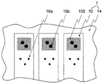
図2は、本発明による第2の接続装置1の膜複合材の第1の主領域の平面図を示している。この図面は、プラスチック膜構造の絶縁層14と、膜複合材の第1の形成部におけるアルミニウムからなる第1の導電層10とを示している。このアルミニウム層10は、本質的に構成され、膜複合材のこの部分に、互いに電気的に絶縁される3つの導体トラックを形成する。これらの導体トラック10の各々は、パッケージされていない半導体構成要素、ここではパワーダイオードを基板の導体トラックに超音波溶接で接続するかまたは半田付け接続するための2群のエンボス加工バンプ16a/bを有する。この構造の代替実施形態は、パワー半導体構成要素だけでなく、接続すべき多数の異なるパッケージされていない構成要素にも適切である。
FIG. 2 shows a plan view of the first main region of the membrane composite of the
第1の構造では、第1群のエンボス加工バンプ16aは、構成要素を、それと同様にアルミニウムから形成されることが好ましい接触領域にスポット溶接で接続するために適切である。第2群のエンボス加工バンプ16bの部分には、電解堆積によってまたは低温ガス噴霧によって堆積されたより薄い銅層102と共に、アルミニウム層が配置される。この銅層102は、基板の導体トラックに半田付け接続するために特に適切である。
In the first structure, the first group of
第2の実施形態(図示せず)では、第2の導電層は銅を含む。このことは、銅が、構成要素からの熱損失をなくすために高い熱伝導率を有し、さらに、高い電流搬送能力のために低い抵抗率を有するので特に好ましい。この場合、溶接接続用の適切な表面を設けるためにアルミニウムからなる第2の層を有する構成要素にスポット溶接で接続するためのエンボス加工バンプ群を形成する必要がある。 In the second embodiment (not shown), the second conductive layer includes copper. This is particularly preferred because copper has a high thermal conductivity to eliminate heat loss from the components and also has a low resistivity for high current carrying capability. In this case, in order to provide an appropriate surface for welding connection, it is necessary to form an embossed bump group for connecting by spot welding to a component having a second layer made of aluminum.
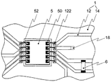
図3は、第2の接続装置1に配置されたパッケージされていない構成要素1を有する構造の本発明による第2の接続装置1の第2の主領域の平面図を示している。この図面は、プラスチック膜構造の絶縁層14と、銅からなる第2の導電層12とを示している。この銅層12は、第1の金属層(図2の10を参照)に比べて本質的により細かく構成され、この部分において、パワー半導体構成要素を駆動するための構成要素5、ここでは駆動回路を接着接合で接続するための領域を形成する。銅層は、さらに、前記駆動回路を接続する多数の導体トラック12を形成する。次に、前記導体トラックは、互いに電気的に絶縁され、かつここでは一例としてキャパシタ6の形態で示したような別の構成要素用の別の接触領域を有する。前記導体トラックは、さらに、0.5〜5μmの厚さを有するここでは金層層の構造の別の金属層122が設けられる部分を有する。金被覆を有するこれらの部分は、駆動回路5の接触領域50と導体トラック12との細いワイヤボンディング接続部52用の好ましい接触領域である。また、膜複合材の第1の導電層へのめっき貫通孔18が示されている。
FIG. 3 shows a plan view of the second main region of the
1 接続装置
2 基板
3a パワー半導体構成要素
3b パワー半導体構成要素
4 構成要素
5 構成要素
6 キャパシタ
10 第1の金属膜
12 第2の金属膜
14 、絶縁膜、プラスチック膜
16a 第1のエンボス加工バンプ
16b 第2のエンボス加工バンプ
18 導電接続部、めっき貫通孔
20 セラミック担体
22 金属導体トラック
32 接触領域
34 接触領域
36 接触領域
40 接触装置
50 接触領域
52 細いワイヤボンディング接続部
102 より薄い銅層
122 別の金属層
DESCRIPTION OF
Claims (10)
前記膜複合材の主領域の少なくとも1つの導電膜(10、12)が、第1の金属を備え、かつ前記膜の厚さに比べて薄い第2金属の層(102、122)を有する少なくとも1つの膜部分を有する接続装置(1)。 A connection device (1) for conductively connecting an electronic component (3a / b, 4, 5, 6) and at least one substrate (2), said connection device (1) comprising at least one insulation Formed as a film composite comprising a film (14) and two conductive films (10, 12), the film composite being arranged in a layer structure of conductive films arranged alternately with insulating films, and at least one conductive A membrane is constructed, thus forming a conductor track,
At least one conductive film (10, 12) in the main region of the membrane composite has at least a second metal layer (102, 122) comprising a first metal and being thinner than the thickness of the membrane. Connecting device (1) having one membrane part.
Applications Claiming Priority (1)
| Application Number | Priority Date | Filing Date | Title |
|---|---|---|---|
| DE102006015198A DE102006015198A1 (en) | 2006-04-01 | 2006-04-01 | Connecting device for electronic components |
Publications (1)
| Publication Number | Publication Date |
|---|---|
| JP2007281452A true JP2007281452A (en) | 2007-10-25 |
Family
ID=38239147
Family Applications (1)
| Application Number | Title | Priority Date | Filing Date |
|---|---|---|---|
| JP2007070666A Pending JP2007281452A (en) | 2006-04-01 | 2007-03-19 | Electronic component connection device |
Country Status (6)
| Country | Link |
|---|---|
| US (1) | US7884287B2 (en) |
| EP (1) | EP1841299A3 (en) |
| JP (1) | JP2007281452A (en) |
| KR (1) | KR101319208B1 (en) |
| CN (1) | CN101055856B (en) |
| DE (1) | DE102006015198A1 (en) |
Cited By (2)
| Publication number | Priority date | Publication date | Assignee | Title |
|---|---|---|---|---|
| JP2010251749A (en) * | 2009-04-11 | 2010-11-04 | Semikron Elektronik Gmbh & Co Kg | Power semiconductor module having connection device and internal terminal element formed as contact spring |
| KR20180089480A (en) * | 2015-12-03 | 2018-08-08 | 콘티넨탈 테베스 아게 운트 코. 오하게 | Electrical conductor tracks, methods and uses |
Families Citing this family (14)
| Publication number | Priority date | Publication date | Assignee | Title |
|---|---|---|---|---|
| US20080221973A1 (en) * | 2005-10-24 | 2008-09-11 | Megdal Myles G | Using commercial share of wallet to rate investments |
| US7838978B2 (en) | 2007-09-19 | 2010-11-23 | Infineon Technologies Ag | Semiconductor device |
| DE102007044620A1 (en) * | 2007-09-19 | 2009-04-16 | Semikron Elektronik Gmbh & Co. Kg | Arrangement with a connection device and at least one semiconductor component |
| DE102007054710B3 (en) | 2007-11-16 | 2009-07-09 | Semikron Elektronik Gmbh & Co. Kg | Method for producing a semiconductor module |
| US8124449B2 (en) | 2008-12-02 | 2012-02-28 | Infineon Technologies Ag | Device including a semiconductor chip and metal foils |
| US20130264721A1 (en) | 2012-04-05 | 2013-10-10 | Infineon Technologies Ag | Electronic Module |
| DE102012007074A1 (en) * | 2012-04-11 | 2013-10-17 | Johnson Electric Germany GmbH & Co. KG | Electrical component with at least one flexible carrier material and method for arranging individual metal bodies on the conductor tracks of a flexible carrier material |
| DE102012218868B3 (en) * | 2012-10-17 | 2013-11-07 | Semikron Elektronik Gmbh & Co. Kg | Power semiconductor module has first and second power semiconductor components that are arranged on common side with respect to first and second direct current (DC) voltage load power connection elements |
| DE102013104949B3 (en) * | 2013-05-14 | 2014-04-24 | Semikron Elektronik Gmbh & Co. Kg | Power electronic switching device and arrangement hereby |
| DE102013213448B4 (en) | 2013-07-09 | 2021-12-09 | Siemens Aktiengesellschaft | Electronic assembly with power semiconductor |
| CN104507264B (en) * | 2014-12-31 | 2017-10-20 | 苏州福莱盈电子有限公司 | It is a kind of to be used for the manufacture craft of 30 microns of fine-lines |
| CN108659245B (en) * | 2018-05-17 | 2020-07-31 | 中国人民解放军国防科技大学 | Shielding reinforced periodic structure |
| DE102019117476B4 (en) * | 2019-06-28 | 2024-03-14 | Semikron Elektronik Gmbh & Co. Kg | Power electronic switching device with a connection element |
| DE102019126265B4 (en) * | 2019-09-30 | 2023-12-14 | Fraunhofer-Gesellschaft zur Förderung der angewandten Forschung e.V. | Device comprising a first carrier substrate and a second carrier substrate, motor vehicle and method for producing a device |
Citations (3)
| Publication number | Priority date | Publication date | Assignee | Title |
|---|---|---|---|---|
| JPH07193098A (en) * | 1993-11-22 | 1995-07-28 | Fujitsu Ltd | Semiconductor device and its manufacture |
| JPH1093017A (en) * | 1996-04-29 | 1998-04-10 | Semikron Elektron Gmbh | High-packaging density semiconductor power module of multi-layer structure system |
| JP2005167241A (en) * | 2003-11-29 | 2005-06-23 | Semikron Elektron Gmbh | Power semiconductor module and its manufacturing method |
Family Cites Families (6)
| Publication number | Priority date | Publication date | Assignee | Title |
|---|---|---|---|---|
| US5121299A (en) * | 1989-12-29 | 1992-06-09 | International Business Machines Corporation | Multi-level circuit structure utilizing conductive cores having conductive protrusions and cavities therein |
| KR0154994B1 (en) * | 1993-11-22 | 1998-12-01 | 세끼자와 다다시 | Semiconductor device and its manufacture |
| JP3197540B2 (en) * | 1999-02-05 | 2001-08-13 | ソニーケミカル株式会社 | Substrate piece and flexible substrate |
| DE10207589A1 (en) * | 2002-02-22 | 2003-10-16 | Leoni Ag | Method for producing a conductor track on a carrier component and carrier component |
| DE10221970A1 (en) | 2002-05-17 | 2003-11-27 | Deutsche Telekom Ag | Microscopic investigation of specimens involves using optical detector with resolution in nanometer range by examining image of specimen formed on light converter that converts it to signal pattern |
| DE10344121A1 (en) * | 2003-09-24 | 2005-04-21 | Daimler Chrysler Ag | Conducting track carrier for motor vehicle, especially for gearbox electronics, has conducting track arrangement manufactured directly on carrier by extrusion |
-
2006
- 2006-04-01 DE DE102006015198A patent/DE102006015198A1/en not_active Withdrawn
-
2007
- 2007-03-15 EP EP07005337A patent/EP1841299A3/en not_active Withdrawn
- 2007-03-19 JP JP2007070666A patent/JP2007281452A/en active Pending
- 2007-03-27 KR KR1020070029614A patent/KR101319208B1/en not_active IP Right Cessation
- 2007-03-30 CN CN2007100898170A patent/CN101055856B/en not_active Expired - Fee Related
- 2007-04-02 US US11/732,002 patent/US7884287B2/en not_active Expired - Fee Related
Patent Citations (3)
| Publication number | Priority date | Publication date | Assignee | Title |
|---|---|---|---|---|
| JPH07193098A (en) * | 1993-11-22 | 1995-07-28 | Fujitsu Ltd | Semiconductor device and its manufacture |
| JPH1093017A (en) * | 1996-04-29 | 1998-04-10 | Semikron Elektron Gmbh | High-packaging density semiconductor power module of multi-layer structure system |
| JP2005167241A (en) * | 2003-11-29 | 2005-06-23 | Semikron Elektron Gmbh | Power semiconductor module and its manufacturing method |
Cited By (3)
| Publication number | Priority date | Publication date | Assignee | Title |
|---|---|---|---|---|
| JP2010251749A (en) * | 2009-04-11 | 2010-11-04 | Semikron Elektronik Gmbh & Co Kg | Power semiconductor module having connection device and internal terminal element formed as contact spring |
| KR20180089480A (en) * | 2015-12-03 | 2018-08-08 | 콘티넨탈 테베스 아게 운트 코. 오하게 | Electrical conductor tracks, methods and uses |
| KR102076924B1 (en) | 2015-12-03 | 2020-02-12 | 콘티넨탈 테베스 아게 운트 코. 오하게 | Electrical conductor track, way |
Also Published As
| Publication number | Publication date |
|---|---|
| KR20070098572A (en) | 2007-10-05 |
| CN101055856B (en) | 2013-01-16 |
| CN101055856A (en) | 2007-10-17 |
| US7884287B2 (en) | 2011-02-08 |
| US20070227767A1 (en) | 2007-10-04 |
| KR101319208B1 (en) | 2013-10-16 |
| EP1841299A3 (en) | 2008-07-09 |
| DE102006015198A1 (en) | 2007-10-11 |
| EP1841299A2 (en) | 2007-10-03 |
Similar Documents
| Publication | Publication Date | Title |
|---|---|---|
| JP2007281452A (en) | Electronic component connection device | |
| US9681558B2 (en) | Module with integrated power electronic circuitry and logic circuitry | |
| US20190304702A1 (en) | Electrical connection contact for a ceramic component, a ceramic component, and a component arrangement | |
| US8415565B2 (en) | Multilayer circuit substrate | |
| US8895871B2 (en) | Circuit board having a plurality of circuit board layers arranged one over the other having bare die mounting for use as a gearbox controller | |
| JP2008060342A5 (en) | ||
| JP2007173680A (en) | Semiconductor device | |
| JP2012099794A (en) | Sintered metal joining, power semiconductor module preferably having sintered silver joining, and manufacturing method of the power semiconductor module | |
| TWI586004B (en) | Circuit for a light emitting component and method of manufacturing the same | |
| EP1780791B1 (en) | Power circuit package and fabrication method | |
| WO2004055891A9 (en) | Semiconductor device and stacked semiconductor device | |
| JP6226068B2 (en) | Semiconductor device | |
| JP2010537397A (en) | Electrical circuit device and method of manufacturing electrical circuit device | |
| US6806563B2 (en) | Composite capacitor and stiffener for chip carrier | |
| JPH08148839A (en) | Hybrid integrated circuit device | |
| JP2008071963A (en) | Multilayer wiring substrate | |
| US20020153608A1 (en) | Land grid array semiconductor device and method of mounting land grid array semiconductor devices | |
| US9681537B2 (en) | Method for producing a power printed circuit and power printed circuit obtained by this method | |
| JP2005032763A (en) | Semiconductor device | |
| JP4527292B2 (en) | Semiconductor power module | |
| JP2005026524A (en) | Semiconductor device and method of manufacturing the same | |
| US20100071947A1 (en) | Multilayer circuit board and motor driving circuit board | |
| US20080311360A1 (en) | Thick film circuit component and method for manufacturing the same | |
| JP2023536196A (en) | electronic circuit module | |
| JP2007067318A (en) | Mounting structure of semiconductor device, and mounting method of the semiconductor device |
Legal Events
| Date | Code | Title | Description |
|---|---|---|---|
| A621 | Written request for application examination |
Free format text: JAPANESE INTERMEDIATE CODE: A621 Effective date: 20091222 |
|
| A977 | Report on retrieval |
Free format text: JAPANESE INTERMEDIATE CODE: A971007 Effective date: 20100406 |
|
| A131 | Notification of reasons for refusal |
Free format text: JAPANESE INTERMEDIATE CODE: A131 Effective date: 20120214 |
|
| A521 | Request for written amendment filed |
Free format text: JAPANESE INTERMEDIATE CODE: A523 Effective date: 20120510 |
|
| A131 | Notification of reasons for refusal |
Free format text: JAPANESE INTERMEDIATE CODE: A131 Effective date: 20120807 |
|
| A02 | Decision of refusal |
Free format text: JAPANESE INTERMEDIATE CODE: A02 Effective date: 20130205 |