EP2166562A2 - Method for forming a capacitor having a strontium/barium titanium oxide dielectric layer by means of ALD and memory device comprising such a capacitor - Google Patents
Method for forming a capacitor having a strontium/barium titanium oxide dielectric layer by means of ALD and memory device comprising such a capacitor Download PDFInfo
- Publication number
- EP2166562A2 EP2166562A2 EP09075435A EP09075435A EP2166562A2 EP 2166562 A2 EP2166562 A2 EP 2166562A2 EP 09075435 A EP09075435 A EP 09075435A EP 09075435 A EP09075435 A EP 09075435A EP 2166562 A2 EP2166562 A2 EP 2166562A2
- Authority
- EP
- European Patent Office
- Prior art keywords
- films
- capacitor
- insulating layer
- bottom electrode
- rich
- Prior art date
- Legal status (The legal status is an assumption and is not a legal conclusion. Google has not performed a legal analysis and makes no representation as to the accuracy of the status listed.)
- Granted
Links
Images





Classifications
-
- H—ELECTRICITY
- H10—SEMICONDUCTOR DEVICES; ELECTRIC SOLID-STATE DEVICES NOT OTHERWISE PROVIDED FOR
- H10P—GENERIC PROCESSES OR APPARATUS FOR THE MANUFACTURE OR TREATMENT OF DEVICES COVERED BY CLASS H10
- H10P14/00—Formation of materials, e.g. in the shape of layers or pillars
- H10P14/60—Formation of materials, e.g. in the shape of layers or pillars of insulating materials
- H10P14/69—Inorganic materials
- H10P14/692—Inorganic materials composed of oxides, glassy oxides or oxide-based glasses
- H10P14/6938—Inorganic materials composed of oxides, glassy oxides or oxide-based glasses the material containing at least one metal element, e.g. metal oxides, metal oxynitrides or metal oxycarbides
- H10P14/69398—Inorganic materials composed of oxides, glassy oxides or oxide-based glasses the material containing at least one metal element, e.g. metal oxides, metal oxynitrides or metal oxycarbides the material having a perovskite structure, e.g. BaTiO3
-
- C—CHEMISTRY; METALLURGY
- C23—COATING METALLIC MATERIAL; COATING MATERIAL WITH METALLIC MATERIAL; CHEMICAL SURFACE TREATMENT; DIFFUSION TREATMENT OF METALLIC MATERIAL; COATING BY VACUUM EVAPORATION, BY SPUTTERING, BY ION IMPLANTATION OR BY CHEMICAL VAPOUR DEPOSITION, IN GENERAL; INHIBITING CORROSION OF METALLIC MATERIAL OR INCRUSTATION IN GENERAL
- C23C—COATING METALLIC MATERIAL; COATING MATERIAL WITH METALLIC MATERIAL; SURFACE TREATMENT OF METALLIC MATERIAL BY DIFFUSION INTO THE SURFACE, BY CHEMICAL CONVERSION OR SUBSTITUTION; COATING BY VACUUM EVAPORATION, BY SPUTTERING, BY ION IMPLANTATION OR BY CHEMICAL VAPOUR DEPOSITION, IN GENERAL
- C23C16/00—Chemical coating by decomposition of gaseous compounds, without leaving reaction products of surface material in the coating, i.e. chemical vapour deposition [CVD] processes
- C23C16/22—Chemical coating by decomposition of gaseous compounds, without leaving reaction products of surface material in the coating, i.e. chemical vapour deposition [CVD] processes characterised by the deposition of inorganic material, other than metallic material
- C23C16/30—Deposition of compounds, mixtures or solid solutions, e.g. borides, carbides, nitrides
- C23C16/40—Oxides
- C23C16/409—Oxides of the type ABO3 with A representing alkali, alkaline earth metal or lead and B representing a refractory metal, nickel, scandium or a lanthanide
-
- C—CHEMISTRY; METALLURGY
- C23—COATING METALLIC MATERIAL; COATING MATERIAL WITH METALLIC MATERIAL; CHEMICAL SURFACE TREATMENT; DIFFUSION TREATMENT OF METALLIC MATERIAL; COATING BY VACUUM EVAPORATION, BY SPUTTERING, BY ION IMPLANTATION OR BY CHEMICAL VAPOUR DEPOSITION, IN GENERAL; INHIBITING CORROSION OF METALLIC MATERIAL OR INCRUSTATION IN GENERAL
- C23C—COATING METALLIC MATERIAL; COATING MATERIAL WITH METALLIC MATERIAL; SURFACE TREATMENT OF METALLIC MATERIAL BY DIFFUSION INTO THE SURFACE, BY CHEMICAL CONVERSION OR SUBSTITUTION; COATING BY VACUUM EVAPORATION, BY SPUTTERING, BY ION IMPLANTATION OR BY CHEMICAL VAPOUR DEPOSITION, IN GENERAL
- C23C16/00—Chemical coating by decomposition of gaseous compounds, without leaving reaction products of surface material in the coating, i.e. chemical vapour deposition [CVD] processes
- C23C16/44—Chemical coating by decomposition of gaseous compounds, without leaving reaction products of surface material in the coating, i.e. chemical vapour deposition [CVD] processes characterised by the method of coating
- C23C16/455—Chemical coating by decomposition of gaseous compounds, without leaving reaction products of surface material in the coating, i.e. chemical vapour deposition [CVD] processes characterised by the method of coating characterised by the method used for introducing gases into reaction chamber or for modifying gas flows in reaction chamber
- C23C16/45523—Pulsed gas flow or change of composition over time
- C23C16/45525—Atomic layer deposition [ALD]
- C23C16/45527—Atomic layer deposition [ALD] characterized by the ALD cycle, e.g. different flows or temperatures during half-reactions, unusual pulsing sequence, use of precursor mixtures or auxiliary reactants or activations
- C23C16/45531—Atomic layer deposition [ALD] characterized by the ALD cycle, e.g. different flows or temperatures during half-reactions, unusual pulsing sequence, use of precursor mixtures or auxiliary reactants or activations specially adapted for making ternary or higher compositions
-
- H—ELECTRICITY
- H10—SEMICONDUCTOR DEVICES; ELECTRIC SOLID-STATE DEVICES NOT OTHERWISE PROVIDED FOR
- H10B—ELECTRONIC MEMORY DEVICES
- H10B12/00—Dynamic random access memory [DRAM] devices
- H10B12/01—Manufacture or treatment
- H10B12/02—Manufacture or treatment for one transistor one-capacitor [1T-1C] memory cells
- H10B12/03—Making the capacitor or connections thereto
-
- H—ELECTRICITY
- H10—SEMICONDUCTOR DEVICES; ELECTRIC SOLID-STATE DEVICES NOT OTHERWISE PROVIDED FOR
- H10B—ELECTRONIC MEMORY DEVICES
- H10B53/00—Ferroelectric RAM [FeRAM] devices comprising ferroelectric memory capacitors
- H10B53/30—Ferroelectric RAM [FeRAM] devices comprising ferroelectric memory capacitors characterised by the memory core region
-
- H—ELECTRICITY
- H10—SEMICONDUCTOR DEVICES; ELECTRIC SOLID-STATE DEVICES NOT OTHERWISE PROVIDED FOR
- H10D—INORGANIC ELECTRIC SEMICONDUCTOR DEVICES
- H10D1/00—Resistors, capacitors or inductors
- H10D1/60—Capacitors
- H10D1/68—Capacitors having no potential barriers
- H10D1/682—Capacitors having no potential barriers having dielectrics comprising perovskite structures
-
- H—ELECTRICITY
- H10—SEMICONDUCTOR DEVICES; ELECTRIC SOLID-STATE DEVICES NOT OTHERWISE PROVIDED FOR
- H10P—GENERIC PROCESSES OR APPARATUS FOR THE MANUFACTURE OR TREATMENT OF DEVICES COVERED BY CLASS H10
- H10P14/00—Formation of materials, e.g. in the shape of layers or pillars
- H10P14/60—Formation of materials, e.g. in the shape of layers or pillars of insulating materials
- H10P14/63—Formation of materials, e.g. in the shape of layers or pillars of insulating materials characterised by the formation processes
- H10P14/6326—Deposition processes
- H10P14/6342—Liquid deposition, e.g. spin-coating, sol-gel techniques or spray coating
-
- H—ELECTRICITY
- H10—SEMICONDUCTOR DEVICES; ELECTRIC SOLID-STATE DEVICES NOT OTHERWISE PROVIDED FOR
- H10P—GENERIC PROCESSES OR APPARATUS FOR THE MANUFACTURE OR TREATMENT OF DEVICES COVERED BY CLASS H10
- H10P14/00—Formation of materials, e.g. in the shape of layers or pillars
- H10P14/60—Formation of materials, e.g. in the shape of layers or pillars of insulating materials
- H10P14/65—Formation of materials, e.g. in the shape of layers or pillars of insulating materials characterised by treatments performed before or after the formation of the materials
- H10P14/6516—Formation of materials, e.g. in the shape of layers or pillars of insulating materials characterised by treatments performed before or after the formation of the materials of treatments performed after formation of the materials
- H10P14/6544—Formation of materials, e.g. in the shape of layers or pillars of insulating materials characterised by treatments performed before or after the formation of the materials of treatments performed after formation of the materials to change the morphology of the insulating materials, e.g. transformation of an amorphous layer into a crystalline layer
Definitions
- the present disclosure relates to capacitive structures whereby an insulating material is sandwiched between a metal top electrode and a metal bottom electrode.
- capacitive structures are also known as MIM (metal-insulator-metal) capacitive structures.
- MIM metal-insulator-metal
- the present disclosure relates to volatile memory cells comprising such MIM capacitive structures.
- Future dynamic random access memory (DRAM) nodes require Metal-Insulator-Metal capacitors (MIMcaps) having Equivalent Oxide Thicknesses (EOT) less than 0.5 nm and low leakage current densities, i.e. less than 10 -7 A/cm 2 .
- MIMcaps Metal-Insulator-Metal capacitors having Equivalent Oxide Thicknesses (EOT) less than 0.5 nm and low leakage current densities, i.e. less than 10 -7 A/cm 2 .
- K dielectric constant
- STO Sr x TiyO 3
- ALD atomic layer deposition
- United States patent US 7,108,747 discloses an Atomic Layer Deposition (ALD) process for producing SrTiO 3 thin films.
- United States patent application US2006/0219157 also discloses an Atomic Layer Deposition (ALD) process for producing titanium containing oxide thin films.
- a metal-insulator-metal capacitor comprising a stack of a bottom electrode , an insulating layer and a top electrode, whereby the insulating layer is a [Ba 1-q Sr q ] x Ti y O z oxide, with q, x, y, z being integers, 0 ⁇ q ⁇ 1 and (x/y) > (1/1).
- the [Ba 1-q Sr q ]/Ti ratio (x/y) is larger than 1, and preferably between( 1/1) ⁇ (x/y) ⁇ (4/1).
- the bottom electrode of this metal-insulator-metal capacitor can comprises Ti, preferably consist of TiN.
- a DRAM memory cell comprising a metal-insulator-metal capacitor and a selection device.
- the metal-insulator-metal capacitor comprises a stack of a bottom electrode, an insulating layer and a top electrode, whereby the insulating layer is a [Ba 1-q Srq] x Ti y O z oxide, with q, x, y, z being integers, O ⁇ q ⁇ 1 and (x/y) > (1/1).
- this insulating layer is a Ba x Ti y O z , oxide.
- the [Ba 1-q Sr q ]/Ti ratio (x/y) is larger than 1, and preferably between( 1/1) ⁇ (x/y) ⁇ (4/1).
- the bottom electrode of this metal-insulator-metal capacitor can comprise Ti and preferably consist of TiN.
- a method for manufacturing a metal-insulator-metal capacitor comprising forming a bottom electrode, forming an insulating layer on the bottom electrode, and forming a top electrode on the insulating layer, whereby the insulating layer is a [Ba 1-q Srq] x Ti y O z oxide, with q, x, y, z being integers, O ⁇ q ⁇ 1 and (x/y) > (1/1).
- the [Ba 1-q Sr q ]/Ti ratio (x/y) is larger than 1, and preferably between( 1/1) ⁇ (x/y) ⁇ (4/1).
- the bottom electrode of this metal-insulator-metal capacitor can comprise Ti and preferably consist of TiN.
- the insulating layer can be formed by Atomic Layer Deposition.
- the insulating layer is formed directly on the bottom electrode (TiN), and the method further comprises performing a anneal step on the as-formed insulating layer thereby bringing the insulating layer into the crystalline perovskite phase.
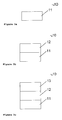
- Figure 1 shows a schematic of a MIM capacitor according to the disclosure.
- Figure 2 shows a DRAM memory cell containing a transistor and a MIM capacitor according to the disclosure.
- Figures 3a-c illustrates, by means of schematic cross-sectional views of process steps, a method for manufacturing MIM capacitor according to the disclosure.
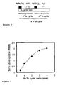
- Figure 4 shows a schematic of the pulse sequence of the ALD STO deposition process for manufacturing MIM capacitor according to a first exemplary embodiment.
- Figure 5 shows the Sr/Ti atomic ratio x/y, determined by RBS, as function of the Sr/Ti pulse ratio (n*/m*) according to a first exemplary embodiment.
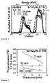
- Figure 6 shows high resolution RBS profiles of STO films for the three compositions illustrated by figure 5 : standard composition (diamonds), Ti-rich (squares), Sr-rich (triangles), according to a first exemplary embodiment.
- Figure 7 shows the perovskite crystallization temperature (°C) as function of the film thickness (nm), for STO films having one of the three compositions illustrated by figure 5 , according to a first exemplary embodiment.
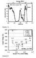
- Figure 8 shows XRD spectra of STO films, having one of the three compositions illustrated by figure 5 , on a ALD TiN bottom electrode: as-deposited (full line), after anneal to 600°C (open circles) and after high temperature anneal (closed circles), according to a first exemplary embodiment.
- Figure 9 shows capacitance-voltage (C-V) and conductance-voltage (G-V) curves of STO films having either the crystalline standard composition or crystalline Sr-rich composition as illustrated by figure 5 for two different STO film thicknesses, according to a first exemplary embodiment.
- Figure 10 shows the EOT-thickness (nm) as function of the physical thickness (nm) for STO films having the Std. Comp., as illustrated in figure 5 , when deposited on a MOCVD TiN bottom electrode after various thermal treatments, according to a first exemplary embodiment.
- Figure 11 shows the capacitance (C) (full symbols) and conductance G (open symbols) as function of the capacitor area (um2) for STO films, having one of the three compositions illustrated by figure 5 , on an ALD TiN bottom electrode: standard composition (diamonds), Ti-rich (squares), Sr-rich (triangles), according to a first exemplary embodiment.
- Figure 12 shows leakage current density (Jg) vs. voltage (V) characteristics for crystallized STO films, having one of the three compositions illustrated by figure 5 , on a ALD TiN bottom electrode: standard composition (diamonds), Ti-rich (squares), Sr-rich (triangles), according to a first exemplary embodiment.
- Figure 13 shows the EOT thickness as function of the physical thickness for a STO film formed on an ALD TiN bottom electrode, the STO film having either the standard composition or the Sr-rich composition as illustrated by figure 5 , according to a first exemplary embodiment.
- Figure 14 shows the leakage current density (Jg) vs. voltage (V) characteristic for 8nm crystallized Sr-rich STO film, as illustrated by figure 5 , on a ALD TiN bottom electrode: standard composition (diamonds), Ti-rich (squares), Sr-rich (triangles), according to a first exemplary embodiment.
- Figure 15 shows the leakage current density (Jg) vs. voltage (V) characteristics for crystallized STO films, having either the standard composition or the Sr-rich composition as illustrated by figure 5 , for different types of bottom electrodes: W, ALD TiN, MOCVD TiN and for different thermal treatments, according to a first exemplary embodiment.
- Figure 16 shows high resolution RBS profiles of Sr x Ti y O 3 films for the various compositions of the STO film according to a second exemplary embodiment.
- Figure 17 shows temperature of crystallization into perovskite Sr x Ti y O 3 phase as a function of STO film composition and thickness according to a second exemplary embodiment.
- the crystallization temperatures are extracted from IS-XRD measurements.
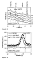
- Figure 18 shows ⁇ -2 ⁇ XRD diagrams of 10 nm Sr x Ti y O 3 films deposited on a TiN bottom electrode with various compositions after high temperature anneal according to a second exemplary embodiment.
- Figure 22 shows XRD diagrams focused on the (200) Bragg peak of 10 nm Sr-rich (3:1) Sr x Ti y O 3 films as-deposited, after anneal at 600°C and after high temperature anneal according to a second exemplary embodiment. As a comparison, the position of reported cubic SrTiO s (200) peak is given.
- Figure 20 shows the equivalent oxide thickness (EOT) vs. physical thickness of as deposited (amorphous) Sr x Ti y O 3 films with various compositions according to a second exemplary embodiment.
- the bottom (respectively top) electrode was TiN (respectively Pt).
- Figure 21 shows the leakage current density (Jg) vs. applied voltage (V) characteristics of 16 nm as deposited (amorphous) Sr x Ti y O 3 films with various compositions according to a second exemplary embodiment.
- the delay time was 10ms.
- Figure 22 shows the capacitance (measured at 0 V, 1 kHz) vs. capacitor area of 10 nm crystalline Sr X Ti y O 3 films with various compositions according to a second exemplary embodiment.
- the crystallization anneal was performed at 600°C for 1 min in N 2 .
- the bottom (respectively top) electrode was TiN (respectively Pt).
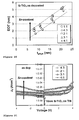
- Figure 23 shows the equivalent oxide thickness (EOT) vs. physical thickness of crystalline Sr x Ti y O 3 films with various compositions according to a second exemplary embodiment.
- the crystallization anneal was performed at 600°C for 1min in N 2 .
- the bottom (respectively top) electrode was TiN (respectively Pt).
- Figure 24 shows the evolution of the dielectric constant (a) and interfacial EOT (b) as a function of the STO film composition according to a second exemplary embodiment.
- the K and interfacial EOT values are extracted form linear fitting of the EOT vs. physical thickness data presented in figure 23 .
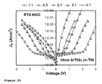
- Figure 25 shows leakage current density (Jg) vs. applied voltage (V) characteristics of 16 nm crystalline Sr x Ti y O 3 films with various compositions according to a second exemplary embodiment.
- the delay time was 550ms.
- the crystallization anneal was performed at 600°C for 1 min in N 2 .
- the bottom (respectively top) electrode was TiN (respectively Pt).
- top, bottom, over, under and the like in the description and the claims are used for descriptive purposes and not necessarily for describing relative positions. The terms so used are interchangeable under appropriate circumstances and the embodiments of the disclosure described herein can operate in other orientations than described or illustrated herein.
- MIM capacitors 10 are formed by sandwiching a layer 12 of insulating material between a metal top electrode 13 and a metal bottom electrode 11 as shown in figure 1 .
- the bottom electrode 11 is the layer in direct physical contact with the insulating layer 12.
- Other layers can be present underneath the bottom electrode 11 to provide a good electrical contact to other devices 20 and/or to provide a diffusion barrier.
- the insulating layer should be formed in a conformal way to provide good step coverage over the underlying bottom electrode 11.
- Such capacitors 10 are used inter alia to form dynamic random access memory cells (DRAM).
- DRAM cells are preferably manufactured using materials, in particular metals, compatible with the processing of logic semiconductor devices such as transistors to allow processing of logic devices and MIM capacitors on the same chip. These materials are available at low-cost and manufacturing-friendly
- An elementary DRAM memory cell 1 consists of a selection element 20, such as transistor, and capacitor 10 as shown in figure 2 .
- the transistor 20 controls the access to the capacitor 10 as this capacitor 10 is connected between one junction of the transistor 10 and ground GND.
- information is saved by storing the corresponding amount of charge on the capacitor 10.
- these memory cells are arranged in a matrix configuration whereby a word line 30 connects the gate of each transistor 10 in the same row, while a bit line 40 connects the other junction each transistor 10 in the same column.
- the material of the insulating layer 12 is selected to have a high value of its relative dielectric constant k and a low leakage current such that information can be temporally stored with limited amount of charge.
- the high relative dielectric constant k of the insulating layer 12 allows obtaining a thin electrical Equivalent Oxide Thickness (EOT) for a physical thicker layer thereby offering a high capacitance value per unit square.
- EOT Equivalent Oxide Thickness
- high-k dielectric is meant a dielectric material having a relative dielectric constant k larger than 1, typically larger than 10.
- the metals of the top 13 and bottom 11 electrodes are selected to help reducing the overall series resistance of the memory cell 1 .
- the process for forming the insulating layer 12 must be compatible with the material used to form the bottom electrode 11. High thermal budgets used to form the insulating layer 12 either during deposition or during post-deposition anneal steps might impact the physical and electrical properties of the bottom electrode 11. Also the ambient in which the insulating layer 12 is formed might influence physical and electrical properties of the bottom electrode 11.
- a Sr x Ti y O z (STO) based Metal-Insulator-Metal (MIM) capacitor 10 is disclosed having an EOT of less than 0.5nm and a leakage current less 5x10 -7 A/cm 2 , preferably less than 1x10 -7 A/cm 2 , when 1V is applied between the top 13 and bottom 11 electrode.
- X, y and z are integers, whereby z is preferably 3 and x/y>1.
- the as-deposited layer thickness of this STO insulating layer 12 is in the range of 5 to 30nm.
- the insulating material 2 as deposited is a strontium-rich Sr x Ti y O z material with x, y,z, being integers.
- Sr-rich Sr x Ti y O z is meant an oxide whereby the Sr-to-Ti ratio x/y is greater than the stoichiometric ratio, i.e. the Sr-to-Ti ratio x/y is greater than 1.
- Figure 5 illustrates examples of such non-stoichiometric Sr x Ti y O 2 material.
- the interface between the Ti-containing bottom electrode 11 and the Sr x Ti y O z insulating layer 12 is essentially free from titanium-oxide such that the Ti-containing bottom electrode 11 is in direct physical contact with this insulating layer 12 .
- titanium-oxide might be present in different crystal orientations on top of the Ti-containing bottom electrode, growing the Sr x Ti y O z having the required properties on top of such titanium-oxide is cumbersome.
- the Sr x Ti y O z based insulating layer 12 of his MIM capacitor 10 is sandwiched between a bottom electrode 11 and a top electrode 13 as shown in figure 1 .
- the insulator 12 of this MIM capacitor 10 comprises an oxide of strontium and titanium and the metal bottom electrode 11 comprises Ti.
- the metal top electrode 13 can be formed from Pt or other metals used in the art to form a top electrode for a MIM capacitor 10.
- this insulator 12 consists of an oxide of strontium and titanium and the metal bottom electrode 11 consists of TiN.
- MIM Metal-Insulator-Metal
- the method comprises forming the insulating layer using a low temperature Atomic Layer Deposition (ALD) process.
- ALD Atomic Layer Deposition
- this ALD process employs an Sr(t-Bu 3 Cp) 2 based precursor system.
- the ALD process is performed at temperatures less than 300°C, preferably 250 °C. This method further requires optimizing the ALD deposition variables, the insulator layer composition and the post-insulator layer deposition processing.
- This manufacturing method allows the use of low-cost, manufacturable-friendly TiN bottom electrodes.
- the electric properties of the capacitor can be tuned as film crystallization temperature, its texture and morphology strongly depends on this ratio.
- the dielectric constant and the leakage current decrease monotonously with the Sr content in the Sr-enriched insulating layer 12.
- the intercept of the EOT vs. physical thickness plot further indicates that increasing the Sr-content at the film interface with the bottom TiN would result in lower interfacial equivalent-oxide thickness (EOT).
- a method for forming such a metal-insulator-metal capacitor 10 whereby the insulator 12 comprises an oxide of strontium and titanium and the metal bottom electrode 11 comprises Ti.
- the method comprises: forming a bottom electrode 11 comprising titanium ( figure 3a ), forming on the bottom electrode 11 an insulating layer 12 comprising an oxide of strontium and titanium ( figure 3b ), and forming on the insulating layer 12 a top electrode 13 whereby the top electrode 13 is electrically isolated from the bottom electrode 11 ( figure 3c ).
- a method for forming such metal-insulator-metal capacitor 10 whereby the insulator 12 consists of an oxide of strontium and titanium and the metal bottom electrode 11 consists of TiN.
- the method comprises: forming a bottom electrode 11 consisting of TiN ( figure 3a ), forming on the bottom electrode 11 an insulating layer 12 consisting of an oxide of strontium and titanium ( figure 3b ), and forming on the insulating layer 12 a top electrode 13 whereby the top electrode 13 is electrically isolated from the bottom electrode 11 ( figure 3c ).
- the insulating layer 12 is in direct physical contact with the bottom electrode 11 and the top electrode 13 is in direct physical contact with the insulating layer 12 .
- a thermal step can be performed to crystallize the insulating layer 12 .
- a Sr-rich Sr x Ti y O z oxide a crystalline oxide can be obtained at temperatures below 600°c, even below 550°C, whereby the high-k perovskite crystalline phase is obtained.
- This crystallization step is preferably performed in a temperature range between 500°C and 600°C, more preferably in a temperature range between 530°C and 570°C, typically at a temperature of about 550°C.
- the bottom electrode 11 containing Ti can be formed by Atomic Layer Deposition (ALD), by Metal-Organic Chemical Vapor Deposition (MOCVD), by Physical Vapor Deposition (PVD) or by other techniques known in the semiconductor process technology.
- ALD Atomic Layer Deposition
- MOCVD Metal-Organic Chemical Vapor Deposition
- PVD Physical Vapor Deposition
- the insulating layer 12 is formed in a low-oxygen ambient, preferably a non-oxidizing ambient, such that the underlying Ti-containing bottom electrode 11 remains essentially oxide-free during the insulating layer forming process.
- This insulating layer 12 can be formed using Atomic Layer Deposition (ALD) with selected precursors allowing the formation of the insulating layer 12 at lower temperatures, i.e. between 200°C and 300°C and in a low oxygen or oxygen-free ambient.
- This precursor is preferably a Sr(t-Bu 3 Cp) 2 based precursor system.
- United States patent US 7,108,747 discloses an Atomic Layer Deposition (ALD) process for producing SrTiO 3 thin films.
- United States patent application US2006/0219157 also discloses an Atomic Layer Deposition (ALD) process for producing titanium containing oxide thin films. Both are incorporated by reference in their entirety.
- the insulating material 12 as deposited is a strontium-rich Sr x Ti y O z material with x, y,z, being integers.
- Sr-rich Sr x Ti y O z is meant an oxide whereby the Sr-to-Ti ratio x/y is greater than the stoichiometric ratio, i.e. the Sr-to-Ti ratio x/y is greater than 1.
- this Sr-to-Ti ratio x/y can be kept substantially equal to the stoichiometric ratio 1, while only during a part of the deposition process this Sr-to-Ti ratio x/y is set higher than the stoichiometric value 1.
- a method for forming such metal-insulator-metal capacitor 10 whereby the insulator 12 consists of an oxide of strontium and titanium and the metal bottom electrode 11 consists of TiN.
- the method comprises: forming a bottom electrode 11 consisting of titanium nitride, forming on the bottom electrode 11 an insulating layer 12 consisting of an oxide of strontium and titanium, and forming on the insulating layer 12 a top electrode 13 whereby the top electrode 13 is electrically isolated from the bottom electrode 11.
- the metal-insulator-metal capacitor 10 shows an Electrical Equivalent Oxide Thickness (EOT) of less than 0.5nm while the leakage current through the insulating layer 12 is less than 500 nA/cm 3 when 1V is applied between the top 13 and bottom 11 electrode.
- EOT Electrical Equivalent Oxide Thickness
- STO layers were deposited by Atomic Layer Deposition (ALD) in a cross-flow ASM Pulsar® 2000 reactor, at reactor temperatures in the 250°C-300°C range.
- the precursors were Sr(t-Bu3Cp)2, H2O, and Ti(OCH3)4.
- the full cycle has to be repeated a number x*, while within each full cycle the number n* of Sr precursor pulses and the number m* of Ti precursor pulses can be selected in view of the desired Sr/Ti ratio within that full cycle as illustrated by figure 4 .
- FIG. 2 shows the Sr/Ti atomic ratio x/y as determined by Rutherford Backscattering (RBS) as function of the Sr/Ti pulse cycle ratio n*/m* thereby referring to the sequence illustrated in figure 4 .
- the STO growth is determined by self-limiting surface reactions, guaranteeing conformal deposition of STO in high aspect ratio structures which is required for advanced DRAM structures.
- STO films 12 in the 7-30 nm range were grown respectively on ALD TiN, MOCVD TiN or W bottom electrodes 11.
- Three different Sr:Ti composition atomic ratios x/y were studied, a "standard composition" close to stoichimoetric atomic ratio (x/y ⁇ 1), a Ti-rich composition (x/y-0.2) and a Sr-rich composition (x/y ⁇ 1.5).
- Figure 6 shows examples of high resolution Rutherford BackScattering (RBS) profiles of STO films 12 on a ALD TiN bottom electrode 11 for the three compositions: standard composition (Std Comp) (diamonds), Ti-rich (squares) and Sr-rich (triangles). As-deposited STO films were amorphous.
- Figure 7 shows the temperature of the 3 STO film 12 types, formed on an ALD TiN bottom electrode 11, as function of the film thickness at which temperature the STO film crystallizes into the perovskite phase.
- the temperature was ramped at 0.2°C/sec.
- the crystallization temperature was higher for the Ti-rich films (x/y-0/2), especially for the thinner films.
- Figure 9 presents typical C-V, G-V curves measured on these STO 12 /ALD TiN 11 films, with the STO film 12 having either the standard composition (x/y ⁇ 1) or the Sr-rich composition (x/y ⁇ 1.5), after Rapid Thermal Anneal (RTA) at 550°C for 60sec in N2.
- RTA Rapid Thermal Anneal
- Figure 11 shows that measured capacitance C and conductance G of annealed crystalline STO films 12 according to figure 5 , sandwiched between an ALD TiN bottom electrode 11 and a Pt top electrode 13.
- the Std Comp and Sr rich STO film were annealed at 550°C, while the Ti rich STO film was annealed at 600°C in line with the discussion above regarding figures 4 and 5 .
- the capacitance C scales linearly with the capacitor area. Extracted values for the EOT are as low as 0.49 nm for a 7.5 nm Sr-rich film (x/y -1.5) and 0.69 nm for a 9 nm Std. Comp. film (x/y ⁇ 1) while the conductance remains low, i.e. exhibiting a low leakage current.
- Figure 12 shows leakage current density Jg - voltage V characteristics for crystallized STO films, having one of the three compositions illustrated by figure 5 , on a ALD TiN bottom electrode: standard composition (diamonds), Ti-rich (squares), Sr-rich (triangles).
- standard composition diamonds
- Ti-rich squares
- Sr-rich triangles
- Figure 13 further compares the electrical characteristics of crystallized STO films with standard (x/y ⁇ 1) and Sr-rich (x/y -1.5) compositions as shown in figure 5 .
- a linear relationship between EOT and physical thicknesses is observed, from which K values can be extracted for both compositions.
- Sr-rich samples show lower K and lower leakage than Std. Comp. films.
- K values for thin films (tphys ⁇ 10nm)
- lower EOTs can be achieved for Sr-rich films which is attributed to a better interface with the underlying TiN bottom electrode 11 .
- Typical leakage current density Jg-V behavior of a MIMcap device 10 composed of a Pt top electrode 13 / a crystallized Sr-rich STO insulating layer 12 /a TiN bottom electrode 11, whereby the insulating layer had EOT of 0.49nm is presented in figure 14 .
- Leakage density values at ⁇ 1V are presented as a function of EOT in figure 15 for crystallized Std. (x/y ⁇ 1) and Sr-rich (x/y-1.5) STO films 12 deposited on TiN (ALD, MOCVD) and W bottom electrodes 11 and after different thermal treatments, showing improvement for films on TiN over recent published data on Ru. 550°C seems to be the optimal anneal temperature, since higher T increases EOT without leakage reduction and lower T results in non crystalline (lower-K) films. Sr-rich composition gives overall lower leakage and lower EOT for thin films than the Std. Comp.
- Sr x Ti y O 3 layers were deposited by atomic layer deposition in a cross-flow ASM Pulsar® 3000 reactor on 300mm Si (100) substrates covered with either 1nm SiO2 or with 20nm SiO2/10nm ALD TiN, at reactor temperatures of 250°C.
- the precursors were Sr(t-Bu 3 Cp) 2 and Ti(OCH 3 ) 4 using H 2 O as an oxidizer.
- the Sr and Ti sources were heated to 180°C and 160°C respectively to ensure a high enough dose for a saturated ALD process.
- the temperature of the H 2 O container was 15°C.
- the vapor pressure was set high enough the achieve STO deposition at temperatures below 300°C.
- ALD By changing the Sr to Ti-precursor ratio, ALD allows the growth of a wide compositional variety of Sr x Ti y O 3 films.
- the ALD process is done in one-step and does not require any seed layer optimization before deposition of the SrTiOx layer.
- Sr x Ti y O 3 films in the 7-20 nm range were grown mainly on ALD TiN substrates.
- Different Sr:Ti pulse ratios n*/m* namely 1:1, 4:3, 3:2, 2:1, 3:1 and 4:1 were studied, resulting in different Sr:Ti composition ratios.
- composition is indicated by giving the pulse ratios.
- the film thicknesses and densities were evaluated by x-ray reflectometry (XRR) while ellipsometry was used to check the uniformity over the wafer (KLA-Tencor ASET F5).
- the composition and contaminant levels of the films were investigated by means of (i) high resolution Rutherford Backscattering Spectrometry (HRRBS); ( ii ) Time-of-Flight Secondary Ion Mass Spectrometry TOFSIMS depth profiles using a ION-TOF IV instrument operating in the dual ion beam mode; and (iii) angle resolved x-ray photoelectron spectroscopy (ARXPS) measurements using a Thermo Theta300 instrument with monochromatized Al K ⁇ radiation (1486.6 eV).
- HRRBS high resolution Rutherford Backscattering Spectrometry
- ARXPS angle resolved x-ray photoelectron spectroscopy
- the Sr x Ti y O 3 crystallization temperature and phase were studied by in situ x-ray diffraction while the film roughness and microstructure were assessed by atomic force microscopy (AFM) using a Veeco Dimension 3100 instrument and by transmission electron microscopy (TEM) using a Tecnai F30 at 300kV.
- the STO crystallization anneal when applied, was performed by rapid thermal annealing (RTA) before the top electrode deposition using a Heat-Pulse system with controlled atmosphere ambient. Electrical measurements were performed using Pt top electrodes (diameters 100-500 ⁇ m) deposited by e-beam evaporation through a shadow mask using a Pfeiffer PLS 580 tool.
- C-V, G-V characteristics were measured with an Agilent 4284A LCR meter while I-V measurements were carried out using a Keithley 2602 multimeter.
- the Keithley 2602 has a limited current accuracy of - 10 pA, but allows for fast, automated screening of samples.
- C-AFM microscopic conductive AFM
- the Veeco Dimension 3100 instrument was converted from AFM to CAFM simply by (i) changing the tips for contact mode imaging by tips with Pt/Ir coating (20-30nm) for electrical measurements and ( ii ) replacing the sense amplifier.
- the optical band gaps of Sr x Ti y O 3 with various Sr-contents were measured by spectroscopic ellipsometry using a Sopra GES 5
- Optical platform with spectral range from 800 to 190nm.
- DFT Density Functional Theory
- the STO film thicknesses and densities were measured using XRR on representative samples before and after crystallization anneals. Typical thickness contraction was about 10% after an anneal of 600°C in N 2 for 1min, the film density increasing from -85% to ⁇ 95% of the bulk value (5.12 g/cm 3 ).
- Figure 16 presents the Sr and Ti HRRBS depth profiles of as deposited 20nm thick Sr x Ti y O 3 films with Sr:Ti ALD pulse ratios ranging from 4:3 (stoichiometric) to 4:1 (67% Sr) .
- Sr and Ti signals were found to be dependent upon the Sr:Ti pulse ratio, the Sr (respectively Ti) signal increasing (respectively decreasing) with increasing the Sr:Ti pulse ratio.
- the extracted film compositions are presented in table 1 below as a function of the ALD Sr:Ti pulse ratios.
- Table 1 ALD Sr:Ti pulse ratios and corresponding compositions (atomic %) measured by High Resolution Rutherford Backscattering Spectrometry (HRRBS) ALD Pulse ratio (Sr:Ti) Sr/(Sr+Ti) (at. %) from HRRBS 1:1 45 4:3 50 3:2 52 2:1 57 3:1 62 4:1 67
- the composition (Sr:Ti ratio) uniformity over the wafer was excellent «1.4%). Furthermore, the composition was proven not to be affected (within experimental error ⁇ 2%) by a change in the underlying substrate nor by an anneal at 600°C (for 1min in N 2 atmosphere).
- TOFSIMS profiles indicated low C, F and Cl contamination in the bulk of the films.
- the C contaminant level measured by XPS was below the detection limits ( ⁇ 1%).
- the characterization of the Sr x Ti y O 3 films was further completed by ARXPS measurements, showing the presence of SrCO 3 on the film surface. For as deposited films, the SrCO 3 concentration was found to increase with increasing Sr:Ti ALD pulse ratios. This SrCO 3 concentration can be strongly reduced by a thermal treatment at 600°C for 1min in N 2 .
- the crystallization behavior of the Sr x Ti y O 3 films was assessed by in-situ XRD ( ⁇ -2 ⁇ geometry) during ramp anneals (0.2°C/s) in N 2 .
- As-deposited Sr x Ti y O 3 films are amorphous and crystallize into the perovskite STO phase at temperatures in the 520-640°C range.
- the crystallization temperature strongly depends on film composition and thickness as show in figure 17 .
- Stoichiometric SrTiO 3 [Sr/(Sr+Ti)] ⁇ 0.5 shows the lowest crystallization temperature for a given thickness. As expected, thinner films require a higher temperature to crystallize but the impact of thickness on crystallization temperature seems more pronounced when increasing the Ti-content.
- In-situ XRD reveals two other noticeable features regarding the impact of composition on the crystallization behavior of Sr x Ti y O 3 films. While all films crystallize into the perovskite structure, the relative intensities of the Sr x Ti y O 3 Bragg peaks change drastically with composition. To better illustrate that point, ⁇ -2 ⁇ scans were taken after the complete ramp anneal as shown in figure 18 .
- Stoichiometric SrTiO 3 films deposited on TiN exhibit a XRD pattern close to the one reported for bulk polycrystalline SrTiO 3 films.
- strontium induces a change in the texture of the films; Sr-rich films being more (200) oriented. This effect is strongly related to the underlying layer as no drastic texture change was observed when depositing SrTiO 3 with the same processing parameters directly on Si.
- Sr-rich films when annealed at 700°C for 1min in N 2 , Sr-rich films exhibit the formation of large Sr-rich crystals.
- Sr-rich films are crystalline (grain size ⁇ 40nm) as can been seen in the TEM cross sections and in agreement with IS-XRD results but there is no formation of Sr-rich crystals.
- Sr-rich STO films At 550°C the Sr-rich STO films are still amorphous.
- Figure 20 shows the EOT evolution of as-deposited films with various Sr:Ti ratios as a function of their physical thickness.
- the extracted relative dielectric K values range from 16 to 18.
- the EOT value increases systematically with increasing Sr-content. This indicates that the interface between Sr x Ti y O 3 layers and the electrodes is sensitive to the film composition. It is believed that the SrCO 3 layers observed on the film surfaces might be responsible of that EOT penalty; the SrCO 3 amount increasing with the Sr-content.
- Figure 18 shows the leakage current density Jg-V curves of 16 nm as deposited Sr x Ti y O 3 films with various Sr-contents. Surprisingly, the increase in EOT observed for Sr-rich films is linked with an increase in the leakage current. This observation suggests differences in the barrier height between the Sr x Ti y O 3 film and the electrodes potentially due to the various SrCO 3 amounts observed in the films.
- Figure 19 shows the capacitance (measured at 0V, 1kHz) as a function of capacitor size for crystalline Sr x Ti y O 3 films (annealed at 600°C for 1min in N 2 ) with compositions (Sr/(Sr+Ti)) ranging from 45% to 62%.
- the measured capacitance scales linearly with area (while the conductance remains ⁇ 10 ⁇ S for all capacitor sizes).
- Sr-enrichment of the Sr x Ti y O 3 films results systematically (for a given capacitor size) in lower capacitance.
- Figure 23 further compares the electrical characteristics of a MIM capacitor having a stack of a Pt top electrode 13 /a Sr x Ti y O 3 insulating layer 12 /a TiN bottom electrode 13 capacitors with various ALD pulse ratios and thicknesses after crystallization anneal at 600°C.
- a linear relationship between EOT and physical thickness is observed.
- the Sr-content has a significant impact on the proportionality factors between EOT and physical thicknesses.
- the extracted relative dielectric constant K values are presented in figure 24a as a function of Sr x Ti y O 3 composition.
- the dielectric constant decreases monotonously with increasing Sr-content (K-210 for stoichiometric 4:3 films and K-56 for Sr-rich 3:1 films).
- the decrease in K value with increasing Sr content observed experimentally is in qualitative agreement with the trend predicted by ab-initio modeling for the ideal Ruddlesden-Popper phases.
- the extrapolation of EOT to zero t phys shown on figure 24b would suggest a decrease of interfacial EOT with increasing Sr-content.
- the "intrinsic" modification of the Sr x Ti y O 3 band gap as a function of the Sr:Ti ratio was evaluated by means of spectroscopic ellipsometry (for 20nm Sr x Ti y O 3 films deposited on SiO 2 and annealed at 600°C for 1min in N 2 ) .
- the extracted optical band gaps increase (from 3.7eV to 4eV) with increasing Sr-content (from stoichiometric 3:2 to Sr-rich 4:1) suggests a higher band offset between the high-K STO layer and the electrodes, resulting in lower leakage currents for Sr-rich films.
- the increase of the band gap with increasing Sr-content is also predicted by ab-initio calculations considering that the excess strontium is accommodated in the structure by formation of RP phases.
- the leakage non-uniformity may be attributed either to higher leakage at grain boundaries due to segregation of Sr or Ti for instance, or by micro-cracks in the films.
- the second scenario is at the origin of the observed patterns for the following reasons: ( i ) CAFM investigations have shown that the leakage occurs predominantly in the bulk of the grains and not at grain boundaries; ( ii ) clear cracks have been seen present after annealing at 700°C for stoichiometric films as also observed in Ti-rich films. On the other hand, quite uniform distributions of leakage spots were demonstrated for Sr-rich films suggesting no obvious formation of cracks in these films. The films are very smooth (RMS roughness ⁇ 0.17nm). This is in total agreement with the observations made by SEM.
- a MIMcap device 10 and methods for manufacturing MIMcap device 10 were disclosed having a non-stoichiometric Sr x Ti y O 3 insulating layer 12 sandwiched between a bottom electrode 11, comprising Ti, and a top electrode 13.
- the non-stoichiometric Sr x Ti y O 3 insulating layer 12 has a Sr-to-Ti atomic ratio x/y>1 and is Sr rich.
- Sr also Ba or a combination of Sr and B can be used to form the non-stoichiometric metal-titanium-oxide insulating layer.
Landscapes
- Chemical & Material Sciences (AREA)
- Engineering & Computer Science (AREA)
- Mechanical Engineering (AREA)
- Chemical Kinetics & Catalysis (AREA)
- General Chemical & Material Sciences (AREA)
- Materials Engineering (AREA)
- Metallurgy (AREA)
- Organic Chemistry (AREA)
- Inorganic Chemistry (AREA)
- Manufacturing & Machinery (AREA)
- Semiconductor Memories (AREA)
- Chemical Vapour Deposition (AREA)
- Formation Of Insulating Films (AREA)
- Inorganic Insulating Materials (AREA)
- Semiconductor Integrated Circuits (AREA)
Abstract
The dielectric layer can also comprise Ba in addition to or instead of Sr, with the formulae BaSrTiO respectively BaTiO.
Description
- The present disclosure relates to capacitive structures whereby an insulating material is sandwiched between a metal top electrode and a metal bottom electrode. These capacitive structures are also known as MIM (metal-insulator-metal) capacitive structures. In particular the present disclosure relates to volatile memory cells comprising such MIM capacitive structures.
- Future dynamic random access memory (DRAM) nodes require Metal-Insulator-Metal capacitors (MIMcaps) having Equivalent Oxide Thicknesses (EOT) less than 0.5 nm and low leakage current densities, i.e. less than 10-7 A/cm2.
- Typical high dielectric constant (K) materials, such as ZrO2/Al2O3/ZrO2, used nowadays in fabrication lines are no longer considered as potential solutions for future DRAM nodes because of their too low dielectric constant (K∼40).
- Hence, various materials systems are being explored to manufacture such MIM capacitors, in particular for use in a DRAM memory cell. Among various materials, SrxTiyO3 (STO) appears as a promising candidate. The interest in this material can be explained both by its good dielectric characteristics (K-150-300) and also by recent improvements in the atomic layer deposition (ALD) process enabling the deposition of conformal STO thin films at a reasonably low processing temperature (≤ 300 °C) suitable for high aspect ratio DRAM applications.
- United States patent
US 7,108,747 discloses an Atomic Layer Deposition (ALD) process for producing SrTiO3 thin films. United States patent applicationUS2006/0219157 also discloses an Atomic Layer Deposition (ALD) process for producing titanium containing oxide thin films. - Recently, ALD SrxTiyO3 using Sr(thd)2 as the Sr precursor has been reported with promising results on noble like metal electrodes such as Ru and Pt. Oh Seong Kwon et al discloses in "Atomic Layer Deposition and Electrical Properties of SrTiO3 Thin films Grown using Sr(C11H19O2)2, Ti (Oi-C3H7)4 and H2O" in Journal Of electrochemical Society 154 (6), G127-G133 (2007) a method for growing SrTiO3 (STO) thin films by means of Atomic Layer Deposition (ALD) thereby using particular precursors. The thin dielectric film is grown on a Ru bottom electrode. However, the processes used required either high deposition temperatures (> 350 °C) and/or post-deposition anneals in an oxidizing ambient, making them incompatible with a TiN bottom electrode. Moreover metal such as Ru and Pt are not compatible with state-of-the-art logic semiconductor processing.
- Therefore there is a need to manufacture a metal-insulator-metal capacitor structure having an EOT of 0.5nm or less and a leakage current less than 5x10⁻⁷ A/cm2.
- There is a need to manufacture such capacitor using process steps and materials that are compatible with standard logic semiconductor processing.
- There is a need to form such the insulating layer of such capacitor at temperatures equal to or less than 300°C.
- There is a need to manufacture such a capacitor having a reduced EOT of the interfacial oxide between the insulating layer and the bottom electrode.
- A metal-insulator-metal capacitor is disclosed comprising a stack of a bottom electrode , an insulating layer and a top electrode, whereby the insulating layer is a [Ba1-q Srq]xTiyOz oxide, with q, x, y, z being integers, 0<q<1 and (x/y) > (1/1). Preferably this insulating layer is [Ba1-q Srq]xTiyO3 oxide. If q=1, this insulating layer is a SrxTiyO2 oxide. If q=0, this insulating layer is a BaxTiyOz oxide. The [Ba1-q Srq]/Ti ratio (x/y) is larger than 1, and preferably between( 1/1)< (x/y) <(4/1). The bottom electrode of this metal-insulator-metal capacitor can comprises Ti, preferably consist of TiN.
- A DRAM memory cell is disclosed comprising a metal-insulator-metal capacitor and a selection device. The metal-insulator-metal capacitor comprises a stack of a bottom electrode, an insulating layer and a top electrode, whereby the insulating layer is a [Ba1-q Srq]xTiyOz oxide, with q, x, y, z being integers, O<q<1 and (x/y) > (1/1). Preferably this insulating layer is [Ba1-q Srq]xTiyO3 oxide . If q=1, this insulating layer is a SrxTiyO2 oxide. If q=0 , this insulating layer is a BaxTiyOz, oxide. The [Ba1-q Srq]/Ti ratio (x/y) is larger than 1, and preferably between( 1/1)< (x/y) <(4/1). The bottom electrode of this metal-insulator-metal capacitor can comprise Ti and preferably consist of TiN.
- A method for manufacturing a metal-insulator-metal capacitor is disclosed, the method comprising forming a bottom electrode, forming an insulating layer on the bottom electrode, and forming a top electrode on the insulating layer, whereby the insulating layer is a [Ba1-q Srq]xTiyOz oxide, with q, x, y, z being integers, O<q<1 and (x/y) > (1/1). Preferably this insulating layer is [Ba1-q Srq]xTiyO3 oxide. If q=1, this insulating layer is a SrxTiyOz oxide. If q=0, this insulating layer is a BaxTiyOz oxide. The [Ba1-q Srq]/Ti ratio (x/y) is larger than 1, and preferably between( 1/1)< (x/y) <(4/1). The bottom electrode of this metal-insulator-metal capacitor can comprise Ti and preferably consist of TiN. The insulating layer can be formed by Atomic Layer Deposition. Preferably the insulating layer is formed directly on the bottom electrode (TiN), and the method further comprises performing a anneal step on the as-formed insulating layer thereby bringing the insulating layer into the crystalline perovskite phase.
-
Figure 1 shows a schematic of a MIM capacitor according to the disclosure. -
Figure 2 shows a DRAM memory cell containing a transistor and a MIM capacitor according to the disclosure. -
Figures 3a-c illustrates, by means of schematic cross-sectional views of process steps, a method for manufacturing MIM capacitor according to the disclosure. -
Figure 4 shows a schematic of the pulse sequence of the ALD STO deposition process for manufacturing MIM capacitor according to a first exemplary embodiment. -
Figure 5 shows the Sr/Ti atomic ratio x/y, determined by RBS, as function of the Sr/Ti pulse ratio (n*/m*) according to a first exemplary embodiment. -
Figure 6 shows high resolution RBS profiles of STO films for the three compositions illustrated byfigure 5 : standard composition (diamonds), Ti-rich (squares), Sr-rich (triangles), according to a first exemplary embodiment. -
Figure 7 shows the perovskite crystallization temperature (°C) as function of the film thickness (nm), for STO films having one of the three compositions illustrated byfigure 5 , according to a first exemplary embodiment. -
Figure 8 shows XRD spectra of STO films, having one of the three compositions illustrated byfigure 5 , on a ALD TiN bottom electrode: as-deposited (full line), after anneal to 600°C (open circles) and after high temperature anneal (closed circles), according to a first exemplary embodiment. -
Figure 9 shows capacitance-voltage (C-V) and conductance-voltage (G-V) curves of STO films having either the crystalline standard composition or crystalline Sr-rich composition as illustrated byfigure 5 for two different STO film thicknesses, according to a first exemplary embodiment. -
Figure 10 shows the EOT-thickness (nm) as function of the physical thickness (nm) for STO films having the Std. Comp., as illustrated infigure 5 , when deposited on a MOCVD TiN bottom electrode after various thermal treatments, according to a first exemplary embodiment. -
Figure 11 shows the capacitance (C) (full symbols) and conductance G (open symbols) as function of the capacitor area (um2) for STO films, having one of the three compositions illustrated byfigure 5 , on an ALD TiN bottom electrode: standard composition (diamonds), Ti-rich (squares), Sr-rich (triangles), according to a first exemplary embodiment. -
Figure 12 shows leakage current density (Jg) vs. voltage (V) characteristics for crystallized STO films, having one of the three compositions illustrated byfigure 5 , on a ALD TiN bottom electrode: standard composition (diamonds), Ti-rich (squares), Sr-rich (triangles), according to a first exemplary embodiment. -
Figure 13 shows the EOT thickness as function of the physical thickness for a STO film formed on an ALD TiN bottom electrode, the STO film having either the standard composition or the Sr-rich composition as illustrated byfigure 5 , according to a first exemplary embodiment. -
Figure 14 shows the leakage current density (Jg) vs. voltage (V) characteristic for 8nm crystallized Sr-rich STO film, as illustrated byfigure 5 , on a ALD TiN bottom electrode: standard composition (diamonds), Ti-rich (squares), Sr-rich (triangles), according to a first exemplary embodiment. -
Figure 15 shows the leakage current density (Jg) vs. voltage (V) characteristics for crystallized STO films, having either the standard composition or the Sr-rich composition as illustrated byfigure 5 , for different types of bottom electrodes: W, ALD TiN, MOCVD TiN and for different thermal treatments, according to a first exemplary embodiment. -
Figure 16 shows high resolution RBS profiles of SrxTiyO3 films for the various compositions of the STO film according to a second exemplary embodiment. -
Figure 17 shows temperature of crystallization into perovskite SrxTiyO3 phase as a function of STO film composition and thickness according to a second exemplary embodiment. The crystallization temperatures are extracted from IS-XRD measurements. -
Figure 18 shows θ-2θ XRD diagrams of 10 nm SrxTiyO3 films deposited on a TiN bottom electrode with various compositions after high temperature anneal according to a second exemplary embodiment. -
Figure 22 shows XRD diagrams focused on the (200) Bragg peak of 10 nm Sr-rich (3:1) SrxTiyO3 films as-deposited, after anneal at 600°C and after high temperature anneal according to a second exemplary embodiment. As a comparison, the position of reported cubic SrTiOs (200) peak is given. -
Figure 20 shows the equivalent oxide thickness (EOT) vs. physical thickness of as deposited (amorphous) SrxTiyO3 films with various compositions according to a second exemplary embodiment. The bottom (respectively top) electrode was TiN (respectively Pt). -
Figure 21 shows the leakage current density (Jg) vs. applied voltage (V) characteristics of 16 nm as deposited (amorphous) SrxTiyO3 films with various compositions according to a second exemplary embodiment. The delay time was 10ms. -
Figure 22 shows the capacitance (measured at 0 V, 1 kHz) vs. capacitor area of 10 nm crystalline SrXTiyO3 films with various compositions according to a second exemplary embodiment. The crystallization anneal was performed at 600°C for 1 min in N2. The bottom (respectively top) electrode was TiN (respectively Pt). -
Figure 23 shows the equivalent oxide thickness (EOT) vs. physical thickness of crystalline SrxTiyO3 films with various compositions according to a second exemplary embodiment. The crystallization anneal was performed at 600°C for 1min in N2. The bottom (respectively top) electrode was TiN (respectively Pt). -
Figure 24 shows the evolution of the dielectric constant (a) and interfacial EOT (b) as a function of the STO film composition according to a second exemplary embodiment. The K and interfacial EOT values are extracted form linear fitting of the EOT vs. physical thickness data presented infigure 23 . -
Figure 25 shows leakage current density (Jg) vs. applied voltage (V) characteristics of 16 nm crystalline SrxTiyO3 films with various compositions according to a second exemplary embodiment. The delay time was 550ms. The crystallization anneal was performed at 600°C for 1 min in N2. The bottom (respectively top) electrode was TiN (respectively Pt). - The drawings described are only schematic and are non-limiting. In the drawings, the size of some of the elements may be exaggerated and not drawn on scale for illustrative purposes. The dimensions and the relative dimensions do not necessarily correspond to actual reductions to practice of the disclosure.
- Furthermore, the terms first, second, third and the like in the description and in the claims, are used for distinguishing between similar elements and not necessarily for describing a sequential or chronological order. The terms are interchangeable under appropriate circumstances and the embodiments of the disclosure can operate in other sequences than described or illustrated herein.
- Moreover, the terms top, bottom, over, under and the like in the description and the claims are used for descriptive purposes and not necessarily for describing relative positions. The terms so used are interchangeable under appropriate circumstances and the embodiments of the disclosure described herein can operate in other orientations than described or illustrated herein.
- The term "comprising", used in the claims, should not be interpreted as being restricted to the means listed thereafter; it does not exclude other elements or steps. It needs to be interpreted as specifying the presence of the stated features, integers, steps or components as referred to, but does not preclude the presence or addition of one or more other features, integers, steps or components, or groups thereof. Thus, the scope of the expression "a device comprising means A and B" should not be limited to devices consisting only of components A and B. It means that with respect to the present disclosure, the only relevant components of the device are A and B.
-
MIM capacitors 10 are formed by sandwiching alayer 12 of insulating material between a metaltop electrode 13 and ametal bottom electrode 11 as shown infigure 1 . Thebottom electrode 11 is the layer in direct physical contact with the insulatinglayer 12. Other layers can be present underneath thebottom electrode 11 to provide a good electrical contact toother devices 20 and/or to provide a diffusion barrier. The insulating layer should be formed in a conformal way to provide good step coverage over theunderlying bottom electrode 11.Such capacitors 10 are used inter alia to form dynamic random access memory cells (DRAM). DRAM cells are preferably manufactured using materials, in particular metals, compatible with the processing of logic semiconductor devices such as transistors to allow processing of logic devices and MIM capacitors on the same chip. These materials are available at low-cost and manufacturing-friendly - An elementary
DRAM memory cell 1 consists of aselection element 20, such as transistor, andcapacitor 10 as shown infigure 2 . Thetransistor 20 controls the access to thecapacitor 10 as thiscapacitor 10 is connected between one junction of thetransistor 10 and ground GND. In such a memory cell information is saved by storing the corresponding amount of charge on thecapacitor 10. Typically these memory cells are arranged in a matrix configuration whereby aword line 30 connects the gate of eachtransistor 10 in the same row, while abit line 40 connects the other junction eachtransistor 10 in the same column. - The material of the insulating
layer 12 is selected to have a high value of its relative dielectric constant k and a low leakage current such that information can be temporally stored with limited amount of charge. The high relative dielectric constant k of the insulatinglayer 12 allows obtaining a thin electrical Equivalent Oxide Thickness (EOT) for a physical thicker layer thereby offering a high capacitance value per unit square. With high-k dielectric is meant a dielectric material having a relative dielectric constant k larger than 1, typically larger than 10. - The metals of the top 13 and bottom 11 electrodes are selected to help reducing the overall series resistance of the
memory cell 1. The process for forming the insulatinglayer 12 must be compatible with the material used to form thebottom electrode 11. High thermal budgets used to form the insulatinglayer 12 either during deposition or during post-deposition anneal steps might impact the physical and electrical properties of thebottom electrode 11. Also the ambient in which the insulatinglayer 12 is formed might influence physical and electrical properties of thebottom electrode 11. - A SrxTiyOz (STO) based Metal-Insulator-Metal (MIM)
capacitor 10 is disclosed having an EOT of less than 0.5nm and a leakage current less 5x10⁻⁷ A/cm2, preferably less than 1x10⁻⁷ A/cm2, when 1V is applied between the top 13 and bottom 11 electrode. X, y and z are integers, whereby z is preferably 3 and x/y>1. - The as-deposited layer thickness of this
STO insulating layer 12 is in the range of 5 to 30nm. The Sr-to-Ti ratio x/y >1, preferably between (1/1)< x/y < (4/1). - In a metal-insulator-
metal capacitor 10 according to this disclosure, the insulatingmaterial 2 as deposited is a strontium-rich SrxTiyOz material with x, y,z, being integers. With Sr-rich SrxTiyOz is meant an oxide whereby the Sr-to-Ti ratio x/y is greater than the stoichiometric ratio, i.e. the Sr-to-Ti ratio x/y is greater than 1.Figure 5 illustrates examples of such non-stoichiometric SrxTiyO2 material. - In metal-insulator-
metal capacitors 10 according to this disclosure SrxTiyO2 grains with a Sr content in excess of the stoichiometric ratio x/y=1 may be present in the insulatinglayer 12. These Sr-rich grains may be distributed over the area of thislayer 12 such that leakage paths between thetop electrode 13 and thebottom electrode 11 are prevented or at least the number of such leakage paths is reduced compared to a stoichiometric SrTiO3 insulating layer. As these Sr-rich grains may have a smaller diameter compared to a stoichiometric SrxTiyOz insulating layer 12, the non-stoichiometric layer of this disclosure may show less cracks. - In metal-insulator-
metal capacitors 10 according to this disclosure the interface between the Ti-containingbottom electrode 11 and the SrxTiyOz insulating layer 12 is essentially free from titanium-oxide such that the Ti-containingbottom electrode 11 is in direct physical contact with this insulatinglayer 12. As titanium-oxide might be present in different crystal orientations on top of the Ti-containing bottom electrode, growing the SrxTiyOz having the required properties on top of such titanium-oxide is cumbersome. - The SrxTiyOz based insulating
layer 12 of hisMIM capacitor 10 is sandwiched between abottom electrode 11 and atop electrode 13 as shown infigure 1 . Theinsulator 12 of thisMIM capacitor 10 comprises an oxide of strontium and titanium and themetal bottom electrode 11 comprises Ti. Themetal top electrode 13 can be formed from Pt or other metals used in the art to form a top electrode for aMIM capacitor 10. - In a preferred embodiment this
insulator 12 consists of an oxide of strontium and titanium and themetal bottom electrode 11 consists of TiN. - A method is disclosed for manufacturing SrxTiyO3 based Metal-Insulator-Metal (MIM) capacitors having an EOT of less than 0.5nm and a leakage current less than, preferably less than5x10-7 A/cm2.
- The method comprises forming the insulating layer using a low temperature Atomic Layer Deposition (ALD) process. Preferably this ALD process employs an Sr(t-Bu3Cp)2 based precursor system. The ALD process is performed at temperatures less than 300°C, preferably 250 °C. This method further requires optimizing the ALD deposition variables, the insulator layer composition and the post-insulator layer deposition processing.
- This manufacturing method allows the use of low-cost, manufacturable-friendly TiN bottom electrodes. By varying the Sr/Ti ratio in the SrxTiyOz dielectric layer of the capacitor, the electric properties of the capacitor can be tuned as film crystallization temperature, its texture and morphology strongly depends on this ratio. The dielectric constant and the leakage current decrease monotonously with the Sr content in the Sr-enriched insulating
layer 12. The intercept of the EOT vs. physical thickness plot further indicates that increasing the Sr-content at the film interface with the bottom TiN would result in lower interfacial equivalent-oxide thickness (EOT). - A method is disclosed, illustrated by
figures 3a-c , for forming such a metal-insulator-metal capacitor 10 whereby theinsulator 12 comprises an oxide of strontium and titanium and themetal bottom electrode 11 comprises Ti. The method comprises: forming abottom electrode 11 comprising titanium (figure 3a ), forming on thebottom electrode 11 an insulatinglayer 12 comprising an oxide of strontium and titanium (figure 3b ), and forming on the insulating layer 12 atop electrode 13 whereby thetop electrode 13 is electrically isolated from the bottom electrode 11 (figure 3c ). - In a preferred embodiment a method is disclosed, illustrated by
figures 3a-c , for forming such metal-insulator-metal capacitor 10 whereby theinsulator 12 consists of an oxide of strontium and titanium and themetal bottom electrode 11 consists of TiN. The method comprises: forming abottom electrode 11 consisting of TiN (figure 3a ), forming on thebottom electrode 11 an insulatinglayer 12 consisting of an oxide of strontium and titanium (figure 3b ), and forming on the insulating layer 12 atop electrode 13 whereby thetop electrode 13 is electrically isolated from the bottom electrode 11 (figure 3c ). The insulatinglayer 12 is in direct physical contact with thebottom electrode 11 and thetop electrode 13 is in direct physical contact with the insulatinglayer 12. - Prior to the step of forming the metal top electrode 13 a thermal step can be performed to crystallize the insulating
layer 12. In case of a Sr-rich SrxTiyOz oxide a crystalline oxide can be obtained at temperatures below 600°c, even below 550°C, whereby the high-k perovskite crystalline phase is obtained. This crystallization step is preferably performed in a temperature range between 500°C and 600°C, more preferably in a temperature range between 530°C and 570°C, typically at a temperature of about 550°C. - The
bottom electrode 11 containing Ti can be formed by Atomic Layer Deposition (ALD), by Metal-Organic Chemical Vapor Deposition (MOCVD), by Physical Vapor Deposition (PVD) or by other techniques known in the semiconductor process technology. - The insulating
layer 12 is formed in a low-oxygen ambient, preferably a non-oxidizing ambient, such that the underlying Ti-containingbottom electrode 11 remains essentially oxide-free during the insulating layer forming process. This insulatinglayer 12 can be formed using Atomic Layer Deposition (ALD) with selected precursors allowing the formation of the insulatinglayer 12 at lower temperatures, i.e. between 200°C and 300°C and in a low oxygen or oxygen-free ambient. This precursor is preferably a Sr(t-Bu3Cp)2 based precursor system. - United States patent
US 7,108,747 discloses an Atomic Layer Deposition (ALD) process for producing SrTiO3 thin films. United States patent applicationUS2006/0219157 also discloses an Atomic Layer Deposition (ALD) process for producing titanium containing oxide thin films. Both are incorporated by reference in their entirety. - The insulating
material 12 as deposited is a strontium-rich SrxTiyOz material with x, y,z, being integers. with Sr-rich SrxTiyOz is meant an oxide whereby the Sr-to-Ti ratio x/y is greater than the stoichiometric ratio, i.e. the Sr-to-Ti ratio x/y is greater than 1. - During the step of depositing the SrxTiyOz insulating layer 12 the ratio Sr-to-Ti x/y can be kept higher than the stoichiometric ratio x/y=1. Optionally this Sr-to-Ti ratio x/y can be kept substantially equal to the
stoichiometric ratio 1, while only during a part of the deposition process this Sr-to-Ti ratio x/y is set higher than thestoichiometric value 1. - In a preferred embodiment a method is disclosed for forming such metal-insulator-
metal capacitor 10 whereby theinsulator 12 consists of an oxide of strontium and titanium and themetal bottom electrode 11 consists of TiN. The method comprises: forming abottom electrode 11 consisting of titanium nitride, forming on thebottom electrode 11 an insulatinglayer 12 consisting of an oxide of strontium and titanium, and forming on the insulating layer 12 atop electrode 13 whereby thetop electrode 13 is electrically isolated from thebottom electrode 11. - The metal-insulator-
metal capacitor 10 according to this patent application shows an Electrical Equivalent Oxide Thickness (EOT) of less than 0.5nm while the leakage current through the insulatinglayer 12 is less than 500 nA/cm3 when 1V is applied between the top 13 and bottom 11 electrode. - STO layers were deposited by Atomic Layer Deposition (ALD) in a cross-flow ASM Pulsar® 2000 reactor, at reactor temperatures in the 250°C-300°C range. The precursors were Sr(t-Bu3Cp)2, H2O, and Ti(OCH3)4. In order to make a layer having a predetermined thickness the full cycle has to be repeated a number x*, while within each full cycle the number n* of Sr precursor pulses and the number m* of Ti precursor pulses can be selected in view of the desired Sr/Ti ratio within that full cycle as illustrated by
figure 4 . By changing the Sr-precursor and the Ti-precursor pulse sequence, ALD allows the growth of a wide compositional variety of STO films from pure Ti02 to Sr-rich, with straight forward composition tuning.Figure 2 shows the Sr/Ti atomic ratio x/y as determined by Rutherford Backscattering (RBS) as function of the Sr/Ti pulse cycle ratio n*/m* thereby referring to the sequence illustrated infigure 4 . A pulse cycle ratio n*/m* of about 1.5 corresponds to a stoichiometric SrTiO3 with x=y=1 and z=3. - In ALD, the STO growth is determined by self-limiting surface reactions, guaranteeing conformal deposition of STO in high aspect ratio structures which is required for advanced DRAM structures.
STO films 12 in the 7-30 nm range were grown respectively on ALD TiN, MOCVD TiN orW bottom electrodes 11. Three different Sr:Ti composition atomic ratios x/y were studied, a "standard composition" close to stoichimoetric atomic ratio (x/y∼1), a Ti-rich composition (x/y-0.2) and a Sr-rich composition (x/y∼1.5). -
Figure 6 shows examples of high resolution Rutherford BackScattering (RBS) profiles ofSTO films 12 on a ALDTiN bottom electrode 11 for the three compositions: standard composition (Std Comp) (diamonds), Ti-rich (squares) and Sr-rich (triangles). As-deposited STO films were amorphous. - Careful characterization of the STO crystallization behavior of these three
STO film 12 compositions was achieved by in-situ XRD measurement during ramp anneals in a He ambient whereby the film was annealed in the ALD chamber. All three film composition crystallized into the high-k perovskite STO phase at temperatures in the 540-620°C range. Crystallization of sub-10 nm Std. Comp. (x/y∼1) and Sr-rich (x/y-0.2)films 12 after ex-situ 550°C 1 min anneal in N2 was also verified by cross-sectional TEM.Figure 7 shows the temperature of the 3STO film 12 types, formed on an ALDTiN bottom electrode 11, as function of the film thickness at which temperature the STO film crystallizes into the perovskite phase. The temperature was ramped at 0.2°C/sec. The crystallization temperature was higher for the Ti-rich films (x/y-0/2), especially for the thinner films. - TEM analysis showed, in agreement, that 14 nm Ti-rich films were still mostly amorphous after 550°C anneal. STO peak-positions for Sr-rich films (x/y-1.5) after anneal to 600°C were found to be shifted respect to reported bulk, i.e. very thick STO layers, STO values, but reached the bulk values with higher T annealing.
Figure 8 shows the XRD spectra of three STO film types deposited on ASDTiN bottom electrode 11. The shift is clearly for the thicker Sr-rich STO film, with bulk STO values achieved above 800°C. This suggests Sr may be in solution in STO after low temperature crystallization anneals and expelled out of STO grains at higher temperatures. The RBS data infigure 6 suggests excess Sr may be preferentially close to the bottom TiN interface. - In order to perform an electrical evaluation of three STO film types, after annealing the insulating
STO layer 12 into the crystalline perovskite phase, aPT top electrode 13 on the stack of the respectivecrystalline STO layer 12/TiN bottom electrode 11. -
Figure 9 presents typical C-V, G-V curves measured on theseSTO 12/ALD TiN 11 films, with theSTO film 12 having either the standard composition (x/y∼1) or the Sr-rich composition (x/y∼1.5), after Rapid Thermal Anneal (RTA) at 550°C for 60sec in N2. Flat C-V characteristics with high capacitance densities are observed while conductance values remain low. - The impact of crystallization on the electrical properties of STO films on a MOCVD
TiN bottom electrode 11 is clearly depicted infigure 10 showing the relationship between the EOT thickness (nm) and the physical thickness (nm) for aSTO film 12 having the standard composition (Std. Comp.: x/y∼1) as function of the crystallization anneal step: no anneal i.e. as deposited, anneal 500°C, anneal 550°C and anneal at 600°C. Typical K values obtained for crystalline STO films with Std. Comp. are ∼150. In agreement with the outcome of the in situ XRD measurements illustrated byfigure 8 , an anneal at 500°C is not sufficient to crystallize Std. Comp. STO films which will show a K value comparable to amorphous films (∼20). Similar results were obtained for these STO films when an ALDTiN bottom electrode 12 was used. -
Figure 11 shows that measured capacitance C and conductance G of annealedcrystalline STO films 12 according tofigure 5 , sandwiched between an ALDTiN bottom electrode 11 and aPt top electrode 13. The Std Comp and Sr rich STO film were annealed at 550°C, while the Ti rich STO film was annealed at 600°C in line with the discussion above regardingfigures 4 and 5 . For each type ofSTO film 12, the capacitance C scales linearly with the capacitor area. Extracted values for the EOT are as low as 0.49 nm for a 7.5 nm Sr-rich film (x/y -1.5) and 0.69 nm for a 9 nm Std. Comp. film (x/y∼1) while the conductance remains low, i.e. exhibiting a low leakage current. -
Figure 12 shows leakage current density Jg - voltage V characteristics for crystallized STO films, having one of the three compositions illustrated byfigure 5 , on a ALD TiN bottom electrode: standard composition (diamonds), Ti-rich (squares), Sr-rich (triangles). For the Ti-rich (x/y -0.2) STO film it was difficult to extract the EOT due to the high conductivity/high leakage observed in those films as can be seen infigures 8 and 9 . -
Figure 13 further compares the electrical characteristics of crystallized STO films with standard (x/y∼1) and Sr-rich (x/y -1.5) compositions as shown infigure 5 . A linear relationship between EOT and physical thicknesses is observed, from which K values can be extracted for both compositions. Sr-rich samples show lower K and lower leakage than Std. Comp. films. Despite lower K values, for thin films (tphys<10nm), lower EOTs can be achieved for Sr-rich films which is attributed to a better interface with the underlyingTiN bottom electrode 11. - Typical leakage current density Jg-V behavior of a
MIMcap device 10 composed of aPt top electrode 13/ a crystallized Sr-richSTO insulating layer 12/aTiN bottom electrode 11, whereby the insulating layer had EOT of 0.49nm is presented infigure 14 . An excellent low leakage behavior is observed, with Jg(+1V)=3.5×10⁻⁷ A/cm2 and Jg(-1V)=8.9×10⁻⁷ A/cm2 which are the lowest leakage values reported so far for STO with ∼0.5nm EOT. - Conductive AFM measurements were performed to understand, at a microscopic scale, the leakage paths in the STO films. From these measurements it is concluded that the leakage conduction is through the bulk of grains and follows the topography whereby a higher topography corresponding to a higher leakage. If one compares the density of the leakage spots as obtained by these conductive AFM measurements (Vg=3.2V) of STO films (tphys<10nm) with Std. (x/y∼1) and Sr-rich (x/y-1.5) compositions, one can see that the density of leakage spots is higher for the Std. Comp., in agreement with the I-V curves shown in
figure 12 . - Leakage density values at ±1V are presented as a function of EOT in
figure 15 for crystallized Std. (x/y∼1) and Sr-rich (x/y-1.5)STO films 12 deposited on TiN (ALD, MOCVD) andW bottom electrodes 11 and after different thermal treatments, showing improvement for films on TiN over recent published data on Ru. 550°C seems to be the optimal anneal temperature, since higher T increases EOT without leakage reduction and lower T results in non crystalline (lower-K) films. Sr-rich composition gives overall lower leakage and lower EOT for thin films than the Std. Comp. - SrxTiyO3 layers were deposited by atomic layer deposition in a cross-flow ASM Pulsar® 3000 reactor on 300mm Si (100) substrates covered with either 1nm SiO2 or with 20nm SiO2/10nm ALD TiN, at reactor temperatures of 250°C. The precursors were Sr(t-Bu3Cp)2 and Ti(OCH3)4 using H2O as an oxidizer. The Sr and Ti sources were heated to 180°C and 160°C respectively to ensure a high enough dose for a saturated ALD process. The temperature of the H2O container was 15°C. The vapor pressure was set high enough the achieve STO deposition at temperatures below 300°C. By changing the Sr to Ti-precursor ratio, ALD allows the growth of a wide compositional variety of SrxTiyO3 films. The ALD process is done in one-step and does not require any seed layer optimization before deposition of the SrTiOx layer. SrxTiyO3 films in the 7-20 nm range were grown mainly on ALD TiN substrates. Different Sr:Ti pulse ratios n*/m* namely 1:1, 4:3, 3:2, 2:1, 3:1 and 4:1 were studied, resulting in different Sr:Ti composition ratios. In this exemplary embodiment composition is indicated by giving the pulse ratios.
- The film thicknesses and densities were evaluated by x-ray reflectometry (XRR) while ellipsometry was used to check the uniformity over the wafer (KLA-Tencor ASET F5). The composition and contaminant levels of the films were investigated by means of (i) high resolution Rutherford Backscattering Spectrometry (HRRBS); (ii) Time-of-Flight Secondary Ion Mass Spectrometry TOFSIMS depth profiles using a ION-TOF IV instrument operating in the dual ion beam mode; and (iii) angle resolved x-ray photoelectron spectroscopy (ARXPS) measurements using a Thermo Theta300 instrument with monochromatized Al Kα radiation (1486.6 eV). The SrxTiyO3 crystallization temperature and phase were studied by in situ x-ray diffraction while the film roughness and microstructure were assessed by atomic force microscopy (AFM) using a Veeco Dimension 3100 instrument and by transmission electron microscopy (TEM) using a Tecnai F30 at 300kV. The STO crystallization anneal, when applied, was performed by rapid thermal annealing (RTA) before the top electrode deposition using a Heat-Pulse system with controlled atmosphere ambient. Electrical measurements were performed using Pt top electrodes (diameters 100-500µm) deposited by e-beam evaporation through a shadow mask using a
Pfeiffer PLS 580 tool. C-V, G-V characteristics were measured with an Agilent 4284A LCR meter while I-V measurements were carried out using a Keithley 2602 multimeter. The Keithley 2602 has a limited current accuracy of - 10 pA, but allows for fast, automated screening of samples. To better understand the conduction mechanisms in those films, macroscopic electrical characterizations were complemented by microscopic conductive AFM (C-AFM) measurements. The Veeco Dimension 3100 instrument was converted from AFM to CAFM simply by (i) changing the tips for contact mode imaging by tips with Pt/Ir coating (20-30nm) for electrical measurements and (ii) replacing the sense amplifier. Finally, the optical band gaps of SrxTiyO3 with various Sr-contents were measured by spectroscopic ellipsometry using aSopra GES 5 Optical platform with spectral range from 800 to 190nm. - A first-principles Density Functional Theory (DFT) linear response approach was used to calculate the dielectric constants and band gap of a series of SrxTiyO3 compositions (from stoichiometric to strontium rich): SrTiO3, Sr2TiO4, Sr3Ti2O7 and Sr4Ti3O10.
- The SrxTiyO3 thickness uniformity measured by ellipsometry over 300 mm wafers indicated a within wafer thickness non-uniformity ≤ 2.5%. In addition, the STO film thicknesses and densities were measured using XRR on representative samples before and after crystallization anneals. Typical thickness contraction was about 10% after an anneal of 600°C in N2 for 1min, the film density increasing from -85% to ∼95% of the bulk value (5.12 g/cm3).
-
Figure 16 presents the Sr and Ti HRRBS depth profiles of as deposited 20nm thick SrxTiyO3 films with Sr:Ti ALD pulse ratios ranging from 4:3 (stoichiometric) to 4:1 (67% Sr) . As expected, the Sr and Ti signals were found to be dependent upon the Sr:Ti pulse ratio, the Sr (respectively Ti) signal increasing (respectively decreasing) with increasing the Sr:Ti pulse ratio. The extracted film compositions are presented in table 1 below as a function of the ALD Sr:Ti pulse ratios.Table 1: ALD Sr:Ti pulse ratios and corresponding compositions (atomic %) measured by High Resolution Rutherford Backscattering Spectrometry (HRRBS) ALD Pulse ratio (Sr:Ti) Sr/(Sr+Ti) (at. %)
from HRRBS1:1 45 4:3 50 3:2 52 2:1 57 3:1 62 4:1 67 - The composition (Sr:Ti ratio) uniformity over the wafer was excellent «1.4%). Furthermore, the composition was proven not to be affected (within experimental error ∼ 2%) by a change in the underlying substrate nor by an anneal at 600°C (for 1min in N2 atmosphere). TOFSIMS profiles indicated low C, F and Cl contamination in the bulk of the films. The C contaminant level measured by XPS was below the detection limits (<1%). The characterization of the SrxTiyO3 films was further completed by ARXPS measurements, showing the presence of SrCO3 on the film surface. For as deposited films, the SrCO3 concentration was found to increase with increasing Sr:Ti ALD pulse ratios. This SrCO3 concentration can be strongly reduced by a thermal treatment at 600°C for 1min in N2.
- The crystallization behavior of the SrxTiyO3 films was assessed by in-situ XRD (θ-2θ geometry) during ramp anneals (0.2°C/s) in N2. As-deposited SrxTiyO3 films are amorphous and crystallize into the perovskite STO phase at temperatures in the 520-640°C range. The crystallization temperature strongly depends on film composition and thickness as show in
figure 17 . Stoichiometric SrTiO3 ([Sr/(Sr+Ti)]∼0.5) shows the lowest crystallization temperature for a given thickness. As expected, thinner films require a higher temperature to crystallize but the impact of thickness on crystallization temperature seems more pronounced when increasing the Ti-content. - In-situ XRD reveals two other noticeable features regarding the impact of composition on the crystallization behavior of SrxTiyO3 films. While all films crystallize into the perovskite structure, the relative intensities of the SrxTiyO3 Bragg peaks change drastically with composition. To better illustrate that point, θ-2θ scans were taken after the complete ramp anneal as shown in
figure 18 . Stoichiometric SrTiO3 films deposited on TiN exhibit a XRD pattern close to the one reported for bulk polycrystalline SrTiO3 films. The addition of strontium induces a change in the texture of the films; Sr-rich films being more (200) oriented. This effect is strongly related to the underlying layer as no drastic texture change was observed when depositing SrTiO3 with the same processing parameters directly on Si. - The second observation relies on the fact that the STO peak positions after anneal at 600°C were found to be shifted with respect to the reported bulk perovskite STO values, but approach the bulk values with higher annealing temperature. This effect is present especially for Sr-rich films as shown in
figure 19 (10 nm 3:1 film). This suggests the excess Sr may be in solution in STO after low crystallization temperature anneals and expelled out of STO grains at higher temperature. - To support this assumption, SEM plan view images were taken on 10nm stoichiometric (4:3) and Sr-rich (3:1) films annealed at various temperatures. Stoichiometric films are amorphous for annealing temperature up to 525°C. In agreement with IS-XRD, crystalline features, namely SrTiO3 grains and star-shaped patterns, can be observed at 600°C. The appearance of the star-shaped patterns in the layers has been attributed by TEM analyzes to stress in the layer After crystallization anneal at 700°C for 1min in N2, cracks appear on the film surface of stoichiometric SrTiO3 films. On the other hand, when annealed at 700°C for 1min in N2, Sr-rich films exhibit the formation of large Sr-rich crystals. At 600°C, Sr-rich films are crystalline (grain size ∼40nm) as can been seen in the TEM cross sections and in agreement with IS-XRD results but there is no formation of Sr-rich crystals. At 550°C the Sr-rich STO films are still amorphous. These SEM observations are in good agreement with a scenario involving the presence of excess Sr in solution at low crystallization annealing temperatures and segregation out of the SrTiO3 grains at higher temperatures.
- The electrical properties of as-deposited SrxTiyO3 based capacitors are summarized in
figures 17 and18 . -
Figure 20 shows the EOT evolution of as-deposited films with various Sr:Ti ratios as a function of their physical thickness. Two main conclusions can be drawn based on these results. For all compositions, the EOT varies linearly with the film thickness. Moreover the slope is rather similar for all compositions suggesting that the intrinsic ('bulk") dielectric constant of the amorphous layers is only slightly affected by changes in the film composition. The extracted relative dielectric K values range from 16 to 18. On the other hand, for every given thickness, the EOT value increases systematically with increasing Sr-content. This indicates that the interface between SrxTiyO3 layers and the electrodes is sensitive to the film composition. It is believed that the SrCO3 layers observed on the film surfaces might be responsible of that EOT penalty; the SrCO3 amount increasing with the Sr-content. -
Figure 18 shows the leakage current density Jg-V curves of 16 nm as deposited SrxTiyO3 films with various Sr-contents. Surprisingly, the increase in EOT observed for Sr-rich films is linked with an increase in the leakage current. This observation suggests differences in the barrier height between the SrxTiyO3 film and the electrodes potentially due to the various SrCO3 amounts observed in the films. -
Figure 19 shows the capacitance (measured at 0V, 1kHz) as a function of capacitor size for crystalline SrxTiyO3 films (annealed at 600°C for 1min in N2) with compositions (Sr/(Sr+Ti)) ranging from 45% to 62%. For all compositions, the measured capacitance scales linearly with area (while the conductance remains <10µS for all capacitor sizes). Furthermore, Sr-enrichment of the SrxTiyO3 films results systematically (for a given capacitor size) in lower capacitance. -
Figure 23 further compares the electrical characteristics of a MIM capacitor having a stack of aPt top electrode 13/a SrxTiyO3 insulating layer 12 /aTiN bottom electrode 13 capacitors with various ALD pulse ratios and thicknesses after crystallization anneal at 600°C. As already seen infigure 21 a linear relationship between EOT and physical thickness is observed. Nevertheless, in contrast with as-deposited films, the Sr-content has a significant impact on the proportionality factors between EOT and physical thicknesses. - The extracted relative dielectric constant K values are presented in
figure 24a as a function of SrxTiyO3 composition. The dielectric constant decreases monotonously with increasing Sr-content (K-210 for stoichiometric 4:3 films and K-56 for Sr-rich 3:1 films). The decrease in K value with increasing Sr content observed experimentally is in qualitative agreement with the trend predicted by ab-initio modeling for the ideal Ruddlesden-Popper phases. Furthermore, the extrapolation of EOT to zero tphys shown onfigure 24b would suggest a decrease of interfacial EOT with increasing Sr-content. These extrapolations should be regarded with caution considering possible sources of fluctuations in the EOT extractions. Nevertheless, as already shown onfigure 18 , the texture of the SrxTiyO3 films was proven to vary with the Sr-content. This texture change should not affect drastically the dielectric properties of the bulk SrxTiyO3, considering that SrxTiyO3 has a cubic symmetry, but might corroborate the lower interfacial EOT extrapolated for Sr-rich films. - The leakage properties of 16 nm crystalline SrxTiyO3 films with the different compositions of interest are depicted in
figure 25 . For the same physical thickness, it is clear that Sr-rich films show a much lower leakage current. To better understand this phenomenon, two factors were considered. - The "intrinsic" modification of the SrxTiyO3 band gap as a function of the Sr:Ti ratio was evaluated by means of spectroscopic ellipsometry (for 20nm SrxTiyO3 films deposited on SiO2 and annealed at 600°C for 1min in N2) . The extracted optical band gaps increase (from 3.7eV to 4eV) with increasing Sr-content (from stoichiometric 3:2 to Sr-rich 4:1) suggests a higher band offset between the high-K STO layer and the electrodes, resulting in lower leakage currents for Sr-rich films. Note that the increase of the band gap with increasing Sr-content is also predicted by ab-initio calculations considering that the excess strontium is accommodated in the structure by formation of RP phases.
- To look at possible "extrinsic" factors which could further explain the lower leakages observed for Sr-rich films, conductive AFM measurements were carried out on Ti-rich (1:1 ALD pulse ratio) and Sr-rich (3:1 ALD pulse ratio) films after crystallization anneal at 600°C for 1 in N2. Ti-rich films show non-uniform distribution of the leakage spots. The clustering of leakage paths becomes more apparent with increasing the Ti-rich SrTiO3 film thickness from 10nm to 15nm. Low leakage areas of ∼220-250nm diameter are surrounded by a 2-dimensional network of leakage paths. Similar behavior has been observed on stoichiometric SrTiO3 films. Knowing that the films were all crystalline, the leakage non-uniformity may be attributed either to higher leakage at grain boundaries due to segregation of Sr or Ti for instance, or by micro-cracks in the films. Most likely the second scenario is at the origin of the observed patterns for the following reasons: (i) CAFM investigations have shown that the leakage occurs predominantly in the bulk of the grains and not at grain boundaries; (ii) clear cracks have been seen present after annealing at 700°C for stoichiometric films as also observed in Ti-rich films. On the other hand, quite uniform distributions of leakage spots were demonstrated for Sr-rich films suggesting no obvious formation of cracks in these films. The films are very smooth (RMS roughness ∼0.17nm). This is in total agreement with the observations made by SEM.
- The experimental results systematic study of physical and electrical characterization of SrxTiyO3
thin films 11 deposited onTiN bottom electrode 12 by ALD with various Sr:Ti pulse n*/m* ratios (namely 1:1, 4:3, 3:2, 2:1, 3:1 and 4:1). Several conclusions can be drawn: - (i) The deposition process has been shown to be well controlled in terms of composition and thickness uniformity.
- (ii) Careful composition analysis of the films was done by HRRBS, TOFSIMS and ARXPS. Despite the overall good control of the composition and low levels of bulk contaminants, ARXPS have also shown the presence of SrCO3 at the SrxTiyO3 film surface. The amount of SrCO3 increases with the Sr-content for as deposited films and can be significantly reduced by crystallization anneal.
- (iii) The impact of Sr-content and thickness upon the SrxTiyO3 film crystallization was studied by in situ XRD. The crystallization temperature of stoichiometric films (Sr:Ti = 4:3 or 3:2) has been shown to be lower than for the other SrxTiyO3 compositions. Furthermore, in situ XRD measurements have shown a change in the film texture with increasing Sr content. Also, the diffraction peaks corresponding to Sr-rich SrxTiyO3 films annealed at 600 °C appear at lower angles than the state-of-the-art peak positions of bulk SrTiO3 perovskites. Even if the mechanisms underlying the accommodation of excess Sr by the SrxTiyO3 structure remains unclear, Sr may be in solution in SrxTiyO3 after low temperature crystallization anneals and expelled out of SrTiO3 grains at higher temperatures to form Sr-rich grains.
- (iv) Clear tradeoff between low EOT and low leakage was observed for crystalline films. In the range of studied thicknesses, Sr-rich films show higher EOT (lower K) values and lower leakage current than stoichiometric or Ti-rich films but extrapolation to zero physical thicknesses would suggest lower interfacial EOT for Sr-rich composition. The EOT and leakage dependence upon Sr-content, predicted by ab-initio modeling, were supported by electrical evidences and also by optical band-gap extractions by spectroscopic ellipsometry. C-AFM investigation suggests that the leakage increase observed for Ti-rich films might also originate from microcracks formation in the film possibly due higher stress in the layer.
- The conclude, the above experimental observations show that the physical and electrical properties of SrxTiyO3 are extremely sensitive to the Sr:Ti ratio and prove that a careful choice of the composition is necessary for a targeted device application.
- In the previous paragraphs and embodiments a
MIMcap device 10 and methods formanufacturing MIMcap device 10 were disclosed having a non-stoichiometric SrxTiyO3 insulating layer 12 sandwiched between abottom electrode 11, comprising Ti, and atop electrode 13. The non-stoichiometric SrxTiyO3 insulating layer 12 has a Sr-to-Ti atomic ratio x/y>1 and is Sr rich. Instead of Sr also Ba or a combination of Sr and B can be used to form the non-stoichiometric metal-titanium-oxide insulating layer. Hence the insulatinglayer 12, as discussed in the foregoing paragraphs and embodiments, can generally be described as a [Ba1-q Srq]xTiyOz oxide with q, x, y, z being integers and x/y>1 to obtain a non-stoichiometric oxide which is rich on alkaline earth metal Ba and/or Sr. If q=0, then a Barium-Titanium oxide BaxTiyOz is obtained while, if q=1, the Strontium-Titanium oxide SrxTiyOz is obtained.
Claims (17)
- A metal-insulator-metal capacitor (10) comprising; a stack of a bottom electrode (11), an insulating layer (12), and a top electrode (13), characterized in that: the insulating layer (11) is a [Ba1-q Srq]xTiyOz oxide, with q, x, y, z being integers, 0<q<1 and (x/y) > (1/1).
- The capacitor of claim 1, wherein:z=3, and the insulating layer is [Ba1-q Srq]xTiyO3 oxide.
- The capacitor of claim 1 or 2, wherein:q=1, and the insulating layer is a SrxTiyOz oxide.
- The capacitor of claim 1 or 2, wherein:q=0, and the insulating layer is a BaxTiyOz oxide.
- The capacitor of any of the foregoing claims, wherein:

- The capacitor of any of the foregoing claims, wherein:the bottom electrode (11) comprises Ti.
- The capacitor of claim 6, wherein:the bottom electrode (11) consists of TiN.
- A DRAM memory cell (1) comprisinga metal-insulator-metal capacitor (10), anda transistor (20) device,characterized in that:the capacitor (10) is a capacitor according to any of the foregoing claims.
- A method for manufacturing a metal-insulator-metal capacitor (10), the method comprising;forming a bottom electrode (11),forming an insulating layer (12) on the bottom electrode (11), andforming a top electrode (13) on the insulating layer (12),characterized in that:the insulating layer is a [Ba1-q Srq]xTiyOz oxide, with q, x, y, z being integers, 0<q<1 and (x/y) > (1/1).
- The method of claim 9, wherein:z=3, and the insulating layer is Ba1-q Srq]xTiyO3 oxide.
- The method of claim 9 or 10, wherein:q=1, and the insulating layer is a SrxTiyOz oxide.
- The method of claim 9 or 10, wherein:q=0, and the insulating layer is a BaxTiyOz oxide.
- The method of any of the claims 9 to 12, wherein:

- The method of any of the claims 9 to 13, wherein:the bottom electrode (11) comprises Ti.
- The method of claim 14, wherein:the bottom electrode (11) consists of TiN.
- The method of any of the claims 9 to 15, wherein:the insulating layer (12) is formed by Atomic Layer Deposition.
- The method of any of the claims 9 to 16, wherein:the insulating layer (12) is formed directly on the bottom electrode (TiN), andthe method further comprises:performing a anneal step on the as-formed insulating layer (12) thereby bringing the insulating layer into the crystalline perovskite phase.
Applications Claiming Priority (1)
| Application Number | Priority Date | Filing Date | Title |
|---|---|---|---|
| US9900108P | 2008-09-22 | 2008-09-22 |
Publications (3)
| Publication Number | Publication Date |
|---|---|
| EP2166562A2 true EP2166562A2 (en) | 2010-03-24 |
| EP2166562A3 EP2166562A3 (en) | 2010-08-04 |
| EP2166562B1 EP2166562B1 (en) | 2019-03-20 |
Family
ID=41395895
Family Applications (1)
| Application Number | Title | Priority Date | Filing Date |
|---|---|---|---|
| EP09075435.9A Active EP2166562B1 (en) | 2008-09-22 | 2009-09-22 | Method for forming a capacitor having a strontium titanium oxide dielectric layer by means of ALD |
Country Status (3)
| Country | Link |
|---|---|
| US (1) | US20100072531A1 (en) |
| EP (1) | EP2166562B1 (en) |
| JP (1) | JP2010074172A (en) |
Cited By (2)
| Publication number | Priority date | Publication date | Assignee | Title |
|---|---|---|---|---|
| EP2434531A3 (en) * | 2010-09-28 | 2015-06-10 | Imec | Metal-insulator-metal capacitor and method for manufacturing thereof |
| US20230143124A1 (en) * | 2021-11-09 | 2023-05-11 | Samsung Electronics Co., Ltd. | Capacitor, method of fabricating the capacitor, and electronic device including the capacitor |
Families Citing this family (14)
| Publication number | Priority date | Publication date | Assignee | Title |
|---|---|---|---|---|
| JP5703354B2 (en) * | 2008-11-26 | 2015-04-15 | 株式会社日立国際電気 | Semiconductor device manufacturing method and substrate processing apparatus |
| US8592058B2 (en) * | 2009-06-03 | 2013-11-26 | Intermolecular, Inc. | Methods of forming strontium titanate films |
| JP5692842B2 (en) * | 2010-06-04 | 2015-04-01 | 株式会社日立国際電気 | Semiconductor device manufacturing method and substrate processing apparatus |
| JP5480032B2 (en) * | 2010-06-22 | 2014-04-23 | 株式会社Adeka | Metal compounds, raw materials for forming thin films, and cyclopentadiene compounds |
| US8633118B2 (en) * | 2012-02-01 | 2014-01-21 | Tokyo Electron Limited | Method of forming thin metal and semi-metal layers by thermal remote oxygen scavenging |
| US8865538B2 (en) | 2012-03-30 | 2014-10-21 | Tokyo Electron Limited | Method of integrating buried threshold voltage adjustment layers for CMOS processing |
| US8865581B2 (en) | 2012-10-19 | 2014-10-21 | Tokyo Electron Limited | Hybrid gate last integration scheme for multi-layer high-k gate stacks |
| US10032853B2 (en) | 2014-09-17 | 2018-07-24 | The United States Of America As Represented By The Secretary Of The Army | Microstructural architecture to enable strain relieved non-linear complex oxide thin films |
| US9506153B2 (en) * | 2014-09-17 | 2016-11-29 | The United States Of America As Represented By The Secretary Of The Army | Integrated composite perovskite oxide heterostructure |
| JPWO2017026207A1 (en) * | 2015-08-11 | 2018-05-10 | 株式会社村田製作所 | Capacitor mounted film |
| EP3660933A1 (en) | 2018-11-30 | 2020-06-03 | IMEC vzw | Structure for use in a metal-insulator-metal capacitor |
| KR102194764B1 (en) * | 2019-05-28 | 2020-12-23 | 한국해양대학교 산학협력단 | Semiconductor device including a two-dimensional perovskite dielectric film and manufacturing method thereof |
| EP3840073B1 (en) * | 2019-12-18 | 2024-09-25 | Imec VZW | A method for manufacturing a magnetic structure for a magnetic device showing a giant vcma effect |
| CN111842076A (en) * | 2020-06-24 | 2020-10-30 | 肇庆宏旺金属实业有限公司 | Preparation method of champagne anti-fingerprint stainless steel |
Citations (2)
| Publication number | Priority date | Publication date | Assignee | Title |
|---|---|---|---|---|
| US7108747B1 (en) | 1998-09-11 | 2006-09-19 | Asm International N.V. | Method for growing oxide thin films containing barium and strontium |
| US20060219157A1 (en) | 2001-06-28 | 2006-10-05 | Antti Rahtu | Oxide films containing titanium |
Family Cites Families (9)
| Publication number | Priority date | Publication date | Assignee | Title |
|---|---|---|---|---|
| US6392264B2 (en) * | 1997-07-08 | 2002-05-21 | Hideki Takeuchi | Semiconductor memory device and method of producing the same |
| JP3171170B2 (en) * | 1998-05-25 | 2001-05-28 | 日本電気株式会社 | Thin film capacitor and method of manufacturing the same |
| JP2000236075A (en) * | 1999-02-12 | 2000-08-29 | Sony Corp | Method for manufacturing dielectric capacitor and method for manufacturing semiconductor memory device |
| AU2002213173A1 (en) * | 2000-11-14 | 2002-05-27 | Motorola, Inc. | Semiconductor structure having high dielectric constant material |
| US7316961B2 (en) * | 2004-11-16 | 2008-01-08 | Samsung Electronics Co., Ltd. | Method of manufacturing semiconductor device |
| JP2006310744A (en) * | 2005-03-28 | 2006-11-09 | Fujitsu Ltd | Thin film capacitor and semiconductor device |
| KR100722988B1 (en) * | 2005-08-25 | 2007-05-30 | 주식회사 하이닉스반도체 | Semiconductor device and manufacturing method |
| US20080118731A1 (en) * | 2006-11-16 | 2008-05-22 | Micron Technology, Inc. | Method of forming a structure having a high dielectric constant, a structure having a high dielectric constant, a capacitor including the structure, a method of forming the capacitor |
| US7892964B2 (en) * | 2007-02-14 | 2011-02-22 | Micron Technology, Inc. | Vapor deposition methods for forming a metal-containing layer on a substrate |
-
2009
- 2009-09-22 US US12/564,577 patent/US20100072531A1/en not_active Abandoned
- 2009-09-22 EP EP09075435.9A patent/EP2166562B1/en active Active
- 2009-09-24 JP JP2009219308A patent/JP2010074172A/en active Pending
Patent Citations (2)
| Publication number | Priority date | Publication date | Assignee | Title |
|---|---|---|---|---|
| US7108747B1 (en) | 1998-09-11 | 2006-09-19 | Asm International N.V. | Method for growing oxide thin films containing barium and strontium |
| US20060219157A1 (en) | 2001-06-28 | 2006-10-05 | Antti Rahtu | Oxide films containing titanium |
Cited By (3)
| Publication number | Priority date | Publication date | Assignee | Title |
|---|---|---|---|---|
| EP2434531A3 (en) * | 2010-09-28 | 2015-06-10 | Imec | Metal-insulator-metal capacitor and method for manufacturing thereof |
| US20230143124A1 (en) * | 2021-11-09 | 2023-05-11 | Samsung Electronics Co., Ltd. | Capacitor, method of fabricating the capacitor, and electronic device including the capacitor |
| US12446239B2 (en) * | 2021-11-09 | 2025-10-14 | Samsung Electronics Co., Ltd. | Capacitor, method of fabricating the capacitor, and electronic device including the capacitor |
Also Published As
| Publication number | Publication date |
|---|---|
| US20100072531A1 (en) | 2010-03-25 |
| EP2166562A3 (en) | 2010-08-04 |
| EP2166562B1 (en) | 2019-03-20 |
| JP2010074172A (en) | 2010-04-02 |
Similar Documents
| Publication | Publication Date | Title |
|---|---|---|
| EP2166562B1 (en) | Method for forming a capacitor having a strontium titanium oxide dielectric layer by means of ALD | |
| Ezhilvalavan et al. | Preparation and properties of tantalum pentoxide (Ta2O5) thin films for ultra large scale integrated circuits (ULSIs) application–A review | |
| Kittl et al. | High-k dielectrics for future generation memory devices | |
| US6576967B1 (en) | Semiconductor structure and process for forming a metal oxy-nitride dielectric layer | |
| EP2434531B1 (en) | Method for manufacturing of a metal-insulator-metal capacitor | |
| EP2259305A1 (en) | Capacitor, semiconductor device comprising the same, method for manufacturing the capacitor, and method for manufacturing the semiconductor device | |
| Menou et al. | Composition influence on the physical and electrical properties of SrxTi1− xOy-based metal-insulator-metal capacitors prepared by atomic layer deposition using TiN bottom electrodes | |
| Zhong et al. | Characterization of RuO 2 electrodes on Zr silicate and ZrO 2 dielectrics | |
| Popovici et al. | High-performance ($\text {EOT}< 0.4\text {nm} $, Jg∼ 10− 7 A/cm 2) ALD-deposited Ru\SrTiO 3 stack for next generations DRAM pillar capacitor | |
| EP1183719A1 (en) | Scalable lead zirconium titanate (pzt) thin film material and deposition method, and ferroelectric memory device structures comprising such thin film material | |
| US6335207B1 (en) | Method for fabricating ferroelectric thin film | |
| Cho et al. | Atomic layer deposition of Ta-doped SnO2 films with enhanced dopant distribution for thermally stable capacitor electrode applications | |
| JP4031552B2 (en) | Method for forming film of semiconductor device | |
| Ko et al. | Improved dielectric constant and leakage current characteristics of BaTiO3 thin film on SrRuO3 seed layer | |
| US6504228B1 (en) | Semiconductor device and method for manufacturing the same | |
| WO2003100824A2 (en) | Ferroelectric capacitor and method of manufacturing the same | |
| Choi et al. | Bottom electrode dependence of the properties of (Ba, Sr) TiO3 thin film capacitors | |
| Shye et al. | Effects of post-oxygen plasma treatment on Pt/(Ba, Sr) TiO3/Pt capacitors at low substrate temperatures | |
| KR100682931B1 (en) | Amorphous dielectric film and manufacturing method thereof | |
| Lee et al. | Ir and Ru bottom electrodes for (Ba, Sr) TiO3 thin films deposited by liquid delivery source chemical vapor deposition | |
| Menou et al. | Seed Layer and Multistack Approaches to Reduce Leakage in SrTiO3-Based Metal–Insulator–Metal Capacitors Using TiN Bottom Electrode | |
| KR100335494B1 (en) | Capacitor having a BST dielectric film included copper and manufacturing method thereof | |
| Duenas et al. | Tantalum pentoxide obtained from TaNx and TaSi2 anodisation: an inexpensive and thermally stable high k dielectric | |
| Lukosius et al. | Metal-insulator-metal capacitors with ALD grown SrTiO3: influence of Pt electrodes | |
| KR100624451B1 (en) | Amorphous High-k Thin Film and Manufacturing Method thereof |
Legal Events
| Date | Code | Title | Description |
|---|---|---|---|
| PUAI | Public reference made under article 153(3) epc to a published international application that has entered the european phase |
Free format text: ORIGINAL CODE: 0009012 |
|
| AK | Designated contracting states |
Kind code of ref document: A2 Designated state(s): AT BE BG CH CY CZ DE DK EE ES FI FR GB GR HR HU IE IS IT LI LT LU LV MC MK MT NL NO PL PT RO SE SI SK SM TR |
|
| AX | Request for extension of the european patent |
Extension state: AL BA RS |
|
| PUAL | Search report despatched |
Free format text: ORIGINAL CODE: 0009013 |
|
| AK | Designated contracting states |
Kind code of ref document: A3 Designated state(s): AT BE BG CH CY CZ DE DK EE ES FI FR GB GR HR HU IE IS IT LI LT LU LV MC MK MT NL NO PL PT RO SE SI SK SM TR |
|
| AX | Request for extension of the european patent |
Extension state: AL BA RS |
|
| 17P | Request for examination filed |
Effective date: 20110204 |
|
| R17P | Request for examination filed (corrected) |
Effective date: 20110204 |
|
| 17Q | First examination report despatched |
Effective date: 20131001 |
|
| STAA | Information on the status of an ep patent application or granted ep patent |
Free format text: STATUS: EXAMINATION IS IN PROGRESS |
|
| RAP1 | Party data changed (applicant data changed or rights of an application transferred) |
Owner name: IMEC VZW |
|
| GRAP | Despatch of communication of intention to grant a patent |
Free format text: ORIGINAL CODE: EPIDOSNIGR1 |
|
| STAA | Information on the status of an ep patent application or granted ep patent |
Free format text: STATUS: GRANT OF PATENT IS INTENDED |
|
| RIC1 | Information provided on ipc code assigned before grant |
Ipc: H01L 27/108 20060101ALI20181022BHEP Ipc: H01L 21/02 20060101AFI20181022BHEP Ipc: H01L 27/11507 20100324ALI20181022BHEP Ipc: H01L 49/02 20060101ALI20181022BHEP Ipc: C23C 16/40 20060101ALI20181022BHEP Ipc: H01L 21/8242 20060101ALI20181022BHEP Ipc: C23C 16/455 20060101ALI20181022BHEP Ipc: H01L 21/316 20060101ALI20181022BHEP Ipc: H01L 21/314 20060101ALI20181022BHEP |
|
| INTG | Intention to grant announced |
Effective date: 20181119 |
|
| RIN1 | Information on inventor provided before grant (corrected) |
Inventor name: KITTL, JORGE Inventor name: WOUTERS, DIRK Inventor name: POPOVICI, MIHAELA IOANA Inventor name: MENOU, NICOLAS |
|
| RIC1 | Information provided on ipc code assigned before grant |
Ipc: H01L 49/02 20060101ALI20181022BHEP Ipc: C23C 16/40 20060101ALI20181022BHEP Ipc: H01L 21/02 20060101AFI20181022BHEP Ipc: H01L 21/316 20060101ALI20181022BHEP Ipc: H01L 21/8242 20060101ALI20181022BHEP Ipc: H01L 27/11507 20170101ALI20181022BHEP Ipc: C23C 16/455 20060101ALI20181022BHEP Ipc: H01L 27/108 20060101ALI20181022BHEP Ipc: H01L 21/314 20060101ALI20181022BHEP |
|
| GRAS | Grant fee paid |
Free format text: ORIGINAL CODE: EPIDOSNIGR3 |
|
| RIC1 | Information provided on ipc code assigned before grant |
Ipc: H01L 27/108 20060101ALI20181022BHEP Ipc: H01L 21/02 20060101AFI20181022BHEP Ipc: H01L 27/11507 20170101ALI20181022BHEP Ipc: H01L 21/316 20060101ALI20181022BHEP Ipc: C23C 16/455 20060101ALI20181022BHEP Ipc: H01L 21/314 20060101ALI20181022BHEP Ipc: C23C 16/40 20060101ALI20181022BHEP Ipc: H01L 21/8242 20060101ALI20181022BHEP Ipc: H01L 49/02 20060101ALI20181022BHEP |
|
| GRAA | (expected) grant |
Free format text: ORIGINAL CODE: 0009210 |
|
| STAA | Information on the status of an ep patent application or granted ep patent |
Free format text: STATUS: THE PATENT HAS BEEN GRANTED |
|
| AK | Designated contracting states |
Kind code of ref document: B1 Designated state(s): AT BE BG CH CY CZ DE DK EE ES FI FR GB GR HR HU IE IS IT LI LT LU LV MC MK MT NL NO PL PT RO SE SI SK SM TR |
|
| AX | Request for extension of the european patent |
Extension state: AL BA RS |
|
| REG | Reference to a national code |
Ref country code: GB Ref legal event code: FG4D |
|
| REG | Reference to a national code |
Ref country code: CH Ref legal event code: EP |
|
| REG | Reference to a national code |
Ref country code: DE Ref legal event code: R096 Ref document number: 602009057507 Country of ref document: DE |
|
| REG | Reference to a national code |
Ref country code: AT Ref legal event code: REF Ref document number: 1111366 Country of ref document: AT Kind code of ref document: T Effective date: 20190415 |
|
| REG | Reference to a national code |
Ref country code: IE Ref legal event code: FG4D |
|
| REG | Reference to a national code |
Ref country code: NL Ref legal event code: MP Effective date: 20190320 |
|
| PG25 | Lapsed in a contracting state [announced via postgrant information from national office to epo] |
Ref country code: FI Free format text: LAPSE BECAUSE OF FAILURE TO SUBMIT A TRANSLATION OF THE DESCRIPTION OR TO PAY THE FEE WITHIN THE PRESCRIBED TIME-LIMIT Effective date: 20190320 Ref country code: NO Free format text: LAPSE BECAUSE OF FAILURE TO SUBMIT A TRANSLATION OF THE DESCRIPTION OR TO PAY THE FEE WITHIN THE PRESCRIBED TIME-LIMIT Effective date: 20190620 Ref country code: SE Free format text: LAPSE BECAUSE OF FAILURE TO SUBMIT A TRANSLATION OF THE DESCRIPTION OR TO PAY THE FEE WITHIN THE PRESCRIBED TIME-LIMIT Effective date: 20190320 Ref country code: LT Free format text: LAPSE BECAUSE OF FAILURE TO SUBMIT A TRANSLATION OF THE DESCRIPTION OR TO PAY THE FEE WITHIN THE PRESCRIBED TIME-LIMIT Effective date: 20190320 |
|
| REG | Reference to a national code |
Ref country code: LT Ref legal event code: MG4D |
|
| PG25 | Lapsed in a contracting state [announced via postgrant information from national office to epo] |
Ref country code: LV Free format text: LAPSE BECAUSE OF FAILURE TO SUBMIT A TRANSLATION OF THE DESCRIPTION OR TO PAY THE FEE WITHIN THE PRESCRIBED TIME-LIMIT Effective date: 20190320 Ref country code: HR Free format text: LAPSE BECAUSE OF FAILURE TO SUBMIT A TRANSLATION OF THE DESCRIPTION OR TO PAY THE FEE WITHIN THE PRESCRIBED TIME-LIMIT Effective date: 20190320 Ref country code: NL Free format text: LAPSE BECAUSE OF FAILURE TO SUBMIT A TRANSLATION OF THE DESCRIPTION OR TO PAY THE FEE WITHIN THE PRESCRIBED TIME-LIMIT Effective date: 20190320 Ref country code: BG Free format text: LAPSE BECAUSE OF FAILURE TO SUBMIT A TRANSLATION OF THE DESCRIPTION OR TO PAY THE FEE WITHIN THE PRESCRIBED TIME-LIMIT Effective date: 20190620 Ref country code: GR Free format text: LAPSE BECAUSE OF FAILURE TO SUBMIT A TRANSLATION OF THE DESCRIPTION OR TO PAY THE FEE WITHIN THE PRESCRIBED TIME-LIMIT Effective date: 20190621 |
|
| REG | Reference to a national code |
Ref country code: AT Ref legal event code: MK05 Ref document number: 1111366 Country of ref document: AT Kind code of ref document: T Effective date: 20190320 |
|
| PG25 | Lapsed in a contracting state [announced via postgrant information from national office to epo] |
Ref country code: EE Free format text: LAPSE BECAUSE OF FAILURE TO SUBMIT A TRANSLATION OF THE DESCRIPTION OR TO PAY THE FEE WITHIN THE PRESCRIBED TIME-LIMIT Effective date: 20190320 Ref country code: PT Free format text: LAPSE BECAUSE OF FAILURE TO SUBMIT A TRANSLATION OF THE DESCRIPTION OR TO PAY THE FEE WITHIN THE PRESCRIBED TIME-LIMIT Effective date: 20190720 Ref country code: IT Free format text: LAPSE BECAUSE OF FAILURE TO SUBMIT A TRANSLATION OF THE DESCRIPTION OR TO PAY THE FEE WITHIN THE PRESCRIBED TIME-LIMIT Effective date: 20190320 Ref country code: CZ Free format text: LAPSE BECAUSE OF FAILURE TO SUBMIT A TRANSLATION OF THE DESCRIPTION OR TO PAY THE FEE WITHIN THE PRESCRIBED TIME-LIMIT Effective date: 20190320 Ref country code: RO Free format text: LAPSE BECAUSE OF FAILURE TO SUBMIT A TRANSLATION OF THE DESCRIPTION OR TO PAY THE FEE WITHIN THE PRESCRIBED TIME-LIMIT Effective date: 20190320 Ref country code: SK Free format text: LAPSE BECAUSE OF FAILURE TO SUBMIT A TRANSLATION OF THE DESCRIPTION OR TO PAY THE FEE WITHIN THE PRESCRIBED TIME-LIMIT Effective date: 20190320 Ref country code: ES Free format text: LAPSE BECAUSE OF FAILURE TO SUBMIT A TRANSLATION OF THE DESCRIPTION OR TO PAY THE FEE WITHIN THE PRESCRIBED TIME-LIMIT Effective date: 20190320 |
|
| PG25 | Lapsed in a contracting state [announced via postgrant information from national office to epo] |
Ref country code: SM Free format text: LAPSE BECAUSE OF FAILURE TO SUBMIT A TRANSLATION OF THE DESCRIPTION OR TO PAY THE FEE WITHIN THE PRESCRIBED TIME-LIMIT Effective date: 20190320 Ref country code: PL Free format text: LAPSE BECAUSE OF FAILURE TO SUBMIT A TRANSLATION OF THE DESCRIPTION OR TO PAY THE FEE WITHIN THE PRESCRIBED TIME-LIMIT Effective date: 20190320 |
|
| PG25 | Lapsed in a contracting state [announced via postgrant information from national office to epo] |
Ref country code: AT Free format text: LAPSE BECAUSE OF FAILURE TO SUBMIT A TRANSLATION OF THE DESCRIPTION OR TO PAY THE FEE WITHIN THE PRESCRIBED TIME-LIMIT Effective date: 20190320 Ref country code: IS Free format text: LAPSE BECAUSE OF FAILURE TO SUBMIT A TRANSLATION OF THE DESCRIPTION OR TO PAY THE FEE WITHIN THE PRESCRIBED TIME-LIMIT Effective date: 20190720 |
|
| REG | Reference to a national code |
Ref country code: DE Ref legal event code: R097 Ref document number: 602009057507 Country of ref document: DE |
|
| PLBE | No opposition filed within time limit |
Free format text: ORIGINAL CODE: 0009261 |
|
| STAA | Information on the status of an ep patent application or granted ep patent |
Free format text: STATUS: NO OPPOSITION FILED WITHIN TIME LIMIT |
|
| PG25 | Lapsed in a contracting state [announced via postgrant information from national office to epo] |
Ref country code: DK Free format text: LAPSE BECAUSE OF FAILURE TO SUBMIT A TRANSLATION OF THE DESCRIPTION OR TO PAY THE FEE WITHIN THE PRESCRIBED TIME-LIMIT Effective date: 20190320 |
|
| 26N | No opposition filed |
Effective date: 20200102 |
|
| PG25 | Lapsed in a contracting state [announced via postgrant information from national office to epo] |
Ref country code: SI Free format text: LAPSE BECAUSE OF FAILURE TO SUBMIT A TRANSLATION OF THE DESCRIPTION OR TO PAY THE FEE WITHIN THE PRESCRIBED TIME-LIMIT Effective date: 20190320 |
|
| PG25 | Lapsed in a contracting state [announced via postgrant information from national office to epo] |
Ref country code: TR Free format text: LAPSE BECAUSE OF FAILURE TO SUBMIT A TRANSLATION OF THE DESCRIPTION OR TO PAY THE FEE WITHIN THE PRESCRIBED TIME-LIMIT Effective date: 20190320 |
|
| PG25 | Lapsed in a contracting state [announced via postgrant information from national office to epo] |
Ref country code: MC Free format text: LAPSE BECAUSE OF FAILURE TO SUBMIT A TRANSLATION OF THE DESCRIPTION OR TO PAY THE FEE WITHIN THE PRESCRIBED TIME-LIMIT Effective date: 20190320 |
|
| REG | Reference to a national code |
Ref country code: CH Ref legal event code: PL |
|
| PG25 | Lapsed in a contracting state [announced via postgrant information from national office to epo] |
Ref country code: IE Free format text: LAPSE BECAUSE OF NON-PAYMENT OF DUE FEES Effective date: 20190922 Ref country code: LU Free format text: LAPSE BECAUSE OF NON-PAYMENT OF DUE FEES Effective date: 20190922 Ref country code: LI Free format text: LAPSE BECAUSE OF NON-PAYMENT OF DUE FEES Effective date: 20190930 Ref country code: CH Free format text: LAPSE BECAUSE OF NON-PAYMENT OF DUE FEES Effective date: 20190930 |
|
| REG | Reference to a national code |
Ref country code: BE Ref legal event code: MM Effective date: 20190930 |
|
| PG25 | Lapsed in a contracting state [announced via postgrant information from national office to epo] |
Ref country code: BE Free format text: LAPSE BECAUSE OF NON-PAYMENT OF DUE FEES Effective date: 20190930 |
|
| GBPC | Gb: european patent ceased through non-payment of renewal fee |
Effective date: 20190922 |
|
| PG25 | Lapsed in a contracting state [announced via postgrant information from national office to epo] |
Ref country code: GB Free format text: LAPSE BECAUSE OF NON-PAYMENT OF DUE FEES Effective date: 20190922 |
|
| PG25 | Lapsed in a contracting state [announced via postgrant information from national office to epo] |
Ref country code: CY Free format text: LAPSE BECAUSE OF FAILURE TO SUBMIT A TRANSLATION OF THE DESCRIPTION OR TO PAY THE FEE WITHIN THE PRESCRIBED TIME-LIMIT Effective date: 20190320 |
|
| PG25 | Lapsed in a contracting state [announced via postgrant information from national office to epo] |
Ref country code: MT Free format text: LAPSE BECAUSE OF FAILURE TO SUBMIT A TRANSLATION OF THE DESCRIPTION OR TO PAY THE FEE WITHIN THE PRESCRIBED TIME-LIMIT Effective date: 20190320 Ref country code: HU Free format text: LAPSE BECAUSE OF FAILURE TO SUBMIT A TRANSLATION OF THE DESCRIPTION OR TO PAY THE FEE WITHIN THE PRESCRIBED TIME-LIMIT; INVALID AB INITIO Effective date: 20090922 |
|
| PG25 | Lapsed in a contracting state [announced via postgrant information from national office to epo] |
Ref country code: MK Free format text: LAPSE BECAUSE OF FAILURE TO SUBMIT A TRANSLATION OF THE DESCRIPTION OR TO PAY THE FEE WITHIN THE PRESCRIBED TIME-LIMIT Effective date: 20190320 |
|
| P01 | Opt-out of the competence of the unified patent court (upc) registered |
Effective date: 20230513 |
|
| PGFP | Annual fee paid to national office [announced via postgrant information from national office to epo] |
Ref country code: DE Payment date: 20250820 Year of fee payment: 17 |
|
| PGFP | Annual fee paid to national office [announced via postgrant information from national office to epo] |
Ref country code: FR Payment date: 20250820 Year of fee payment: 17 |
|
| REG | Reference to a national code |
Ref country code: DE Ref legal event code: R079 Ref document number: 602009057507 Country of ref document: DE Free format text: PREVIOUS MAIN CLASS: H01L0021020000 Ipc: H10P0095000000 |