EP2164098A1 - Semiconductor package and method for manufacturing the same - Google Patents
Semiconductor package and method for manufacturing the same Download PDFInfo
- Publication number
- EP2164098A1 EP2164098A1 EP08790715A EP08790715A EP2164098A1 EP 2164098 A1 EP2164098 A1 EP 2164098A1 EP 08790715 A EP08790715 A EP 08790715A EP 08790715 A EP08790715 A EP 08790715A EP 2164098 A1 EP2164098 A1 EP 2164098A1
- Authority
- EP
- European Patent Office
- Prior art keywords
- filter
- substrate
- semiconductor
- cap substrate
- spacer
- Prior art date
- Legal status (The legal status is an assumption and is not a legal conclusion. Google has not performed a legal analysis and makes no representation as to the accuracy of the status listed.)
- Withdrawn
Links
Images




Classifications
-
- H—ELECTRICITY
- H10—SEMICONDUCTOR DEVICES; ELECTRIC SOLID-STATE DEVICES NOT OTHERWISE PROVIDED FOR
- H10W—GENERIC PACKAGES, INTERCONNECTIONS, CONNECTORS OR OTHER CONSTRUCTIONAL DETAILS OF DEVICES COVERED BY CLASS H10
- H10W76/00—Containers; Fillings or auxiliary members therefor; Seals
- H10W76/10—Containers or parts thereof
-
- H—ELECTRICITY
- H10—SEMICONDUCTOR DEVICES; ELECTRIC SOLID-STATE DEVICES NOT OTHERWISE PROVIDED FOR
- H10F—INORGANIC SEMICONDUCTOR DEVICES SENSITIVE TO INFRARED RADIATION, LIGHT, ELECTROMAGNETIC RADIATION OF SHORTER WAVELENGTH OR CORPUSCULAR RADIATION
- H10F77/00—Constructional details of devices covered by this subclass
- H10F77/50—Encapsulations or containers
-
- H—ELECTRICITY
- H10—SEMICONDUCTOR DEVICES; ELECTRIC SOLID-STATE DEVICES NOT OTHERWISE PROVIDED FOR
- H10F—INORGANIC SEMICONDUCTOR DEVICES SENSITIVE TO INFRARED RADIATION, LIGHT, ELECTROMAGNETIC RADIATION OF SHORTER WAVELENGTH OR CORPUSCULAR RADIATION
- H10F39/00—Integrated devices, or assemblies of multiple devices, comprising at least one element covered by group H10F30/00, e.g. radiation detectors comprising photodiode arrays
- H10F39/80—Constructional details of image sensors
- H10F39/804—Containers or encapsulations
-
- H—ELECTRICITY
- H10—SEMICONDUCTOR DEVICES; ELECTRIC SOLID-STATE DEVICES NOT OTHERWISE PROVIDED FOR
- H10F—INORGANIC SEMICONDUCTOR DEVICES SENSITIVE TO INFRARED RADIATION, LIGHT, ELECTROMAGNETIC RADIATION OF SHORTER WAVELENGTH OR CORPUSCULAR RADIATION
- H10F39/00—Integrated devices, or assemblies of multiple devices, comprising at least one element covered by group H10F30/00, e.g. radiation detectors comprising photodiode arrays
- H10F39/80—Constructional details of image sensors
- H10F39/805—Coatings
- H10F39/8053—Colour filters
-
- H—ELECTRICITY
- H10—SEMICONDUCTOR DEVICES; ELECTRIC SOLID-STATE DEVICES NOT OTHERWISE PROVIDED FOR
- H10W—GENERIC PACKAGES, INTERCONNECTIONS, CONNECTORS OR OTHER CONSTRUCTIONAL DETAILS OF DEVICES COVERED BY CLASS H10
- H10W70/00—Package substrates; Interposers; Redistribution layers [RDL]
- H10W70/01—Manufacture or treatment
- H10W70/05—Manufacture or treatment of insulating or insulated package substrates, or of interposers, or of redistribution layers
- H10W70/08—Manufacture or treatment of insulating or insulated package substrates, or of interposers, or of redistribution layers by depositing layers on the chip or wafer, e.g. "chip-first" RDLs
- H10W70/09—Manufacture or treatment of insulating or insulated package substrates, or of interposers, or of redistribution layers by depositing layers on the chip or wafer, e.g. "chip-first" RDLs extending onto an encapsulation that laterally surrounds the chip or wafer, e.g. fan-out wafer level package [FOWLP] RDLs
-
- H—ELECTRICITY
- H10—SEMICONDUCTOR DEVICES; ELECTRIC SOLID-STATE DEVICES NOT OTHERWISE PROVIDED FOR
- H10W—GENERIC PACKAGES, INTERCONNECTIONS, CONNECTORS OR OTHER CONSTRUCTIONAL DETAILS OF DEVICES COVERED BY CLASS H10
- H10W70/00—Package substrates; Interposers; Redistribution layers [RDL]
- H10W70/01—Manufacture or treatment
- H10W70/05—Manufacture or treatment of insulating or insulated package substrates, or of interposers, or of redistribution layers
- H10W70/093—Connecting or disconnecting other interconnections thereto or therefrom, e.g. connecting bond wires or bumps
-
- H—ELECTRICITY
- H10—SEMICONDUCTOR DEVICES; ELECTRIC SOLID-STATE DEVICES NOT OTHERWISE PROVIDED FOR
- H10W—GENERIC PACKAGES, INTERCONNECTIONS, CONNECTORS OR OTHER CONSTRUCTIONAL DETAILS OF DEVICES COVERED BY CLASS H10
- H10W70/00—Package substrates; Interposers; Redistribution layers [RDL]
- H10W70/60—Insulating or insulated package substrates; Interposers; Redistribution layers
-
- H—ELECTRICITY
- H10—SEMICONDUCTOR DEVICES; ELECTRIC SOLID-STATE DEVICES NOT OTHERWISE PROVIDED FOR
- H10W—GENERIC PACKAGES, INTERCONNECTIONS, CONNECTORS OR OTHER CONSTRUCTIONAL DETAILS OF DEVICES COVERED BY CLASS H10
- H10W70/00—Package substrates; Interposers; Redistribution layers [RDL]
- H10W70/60—Insulating or insulated package substrates; Interposers; Redistribution layers
- H10W70/611—Insulating or insulated package substrates; Interposers; Redistribution layers for connecting multiple chips together
- H10W70/614—Insulating or insulated package substrates; Interposers; Redistribution layers for connecting multiple chips together the multiple chips being integrally enclosed
-
- H—ELECTRICITY
- H10—SEMICONDUCTOR DEVICES; ELECTRIC SOLID-STATE DEVICES NOT OTHERWISE PROVIDED FOR
- H10W—GENERIC PACKAGES, INTERCONNECTIONS, CONNECTORS OR OTHER CONSTRUCTIONAL DETAILS OF DEVICES COVERED BY CLASS H10
- H10W76/00—Containers; Fillings or auxiliary members therefor; Seals
- H10W76/10—Containers or parts thereof
- H10W76/12—Containers or parts thereof characterised by their shape
- H10W76/15—Containers comprising an insulating or insulated base
- H10W76/153—Containers comprising an insulating or insulated base having interconnections in passages through the insulating or insulated base
-
- H—ELECTRICITY
- H10—SEMICONDUCTOR DEVICES; ELECTRIC SOLID-STATE DEVICES NOT OTHERWISE PROVIDED FOR
- H10W—GENERIC PACKAGES, INTERCONNECTIONS, CONNECTORS OR OTHER CONSTRUCTIONAL DETAILS OF DEVICES COVERED BY CLASS H10
- H10W76/00—Containers; Fillings or auxiliary members therefor; Seals
- H10W76/40—Fillings or auxiliary members in containers, e.g. centering rings
-
- H—ELECTRICITY
- H10—SEMICONDUCTOR DEVICES; ELECTRIC SOLID-STATE DEVICES NOT OTHERWISE PROVIDED FOR
- H10F—INORGANIC SEMICONDUCTOR DEVICES SENSITIVE TO INFRARED RADIATION, LIGHT, ELECTROMAGNETIC RADIATION OF SHORTER WAVELENGTH OR CORPUSCULAR RADIATION
- H10F39/00—Integrated devices, or assemblies of multiple devices, comprising at least one element covered by group H10F30/00, e.g. radiation detectors comprising photodiode arrays
- H10F39/011—Manufacture or treatment of image sensors covered by group H10F39/12
-
- H—ELECTRICITY
- H10—SEMICONDUCTOR DEVICES; ELECTRIC SOLID-STATE DEVICES NOT OTHERWISE PROVIDED FOR
- H10W—GENERIC PACKAGES, INTERCONNECTIONS, CONNECTORS OR OTHER CONSTRUCTIONAL DETAILS OF DEVICES COVERED BY CLASS H10
- H10W70/00—Package substrates; Interposers; Redistribution layers [RDL]
- H10W70/099—Connecting interconnections to insulating or insulated package substrates, interposers or redistribution layers
-
- H—ELECTRICITY
- H10—SEMICONDUCTOR DEVICES; ELECTRIC SOLID-STATE DEVICES NOT OTHERWISE PROVIDED FOR
- H10W—GENERIC PACKAGES, INTERCONNECTIONS, CONNECTORS OR OTHER CONSTRUCTIONAL DETAILS OF DEVICES COVERED BY CLASS H10
- H10W72/00—Interconnections or connectors in packages
- H10W72/01—Manufacture or treatment
- H10W72/0198—Manufacture or treatment batch processes
-
- H—ELECTRICITY
- H10—SEMICONDUCTOR DEVICES; ELECTRIC SOLID-STATE DEVICES NOT OTHERWISE PROVIDED FOR
- H10W—GENERIC PACKAGES, INTERCONNECTIONS, CONNECTORS OR OTHER CONSTRUCTIONAL DETAILS OF DEVICES COVERED BY CLASS H10
- H10W72/00—Interconnections or connectors in packages
- H10W72/071—Connecting or disconnecting
- H10W72/073—Connecting or disconnecting of die-attach connectors
-
- H—ELECTRICITY
- H10—SEMICONDUCTOR DEVICES; ELECTRIC SOLID-STATE DEVICES NOT OTHERWISE PROVIDED FOR
- H10W—GENERIC PACKAGES, INTERCONNECTIONS, CONNECTORS OR OTHER CONSTRUCTIONAL DETAILS OF DEVICES COVERED BY CLASS H10
- H10W72/00—Interconnections or connectors in packages
- H10W72/20—Bump connectors, e.g. solder bumps or copper pillars; Dummy bumps; Thermal bumps
- H10W72/241—Dispositions, e.g. layouts
-
- H—ELECTRICITY
- H10—SEMICONDUCTOR DEVICES; ELECTRIC SOLID-STATE DEVICES NOT OTHERWISE PROVIDED FOR
- H10W—GENERIC PACKAGES, INTERCONNECTIONS, CONNECTORS OR OTHER CONSTRUCTIONAL DETAILS OF DEVICES COVERED BY CLASS H10
- H10W72/00—Interconnections or connectors in packages
- H10W72/851—Dispositions of multiple connectors or interconnections
- H10W72/874—On different surfaces
-
- H—ELECTRICITY
- H10—SEMICONDUCTOR DEVICES; ELECTRIC SOLID-STATE DEVICES NOT OTHERWISE PROVIDED FOR
- H10W—GENERIC PACKAGES, INTERCONNECTIONS, CONNECTORS OR OTHER CONSTRUCTIONAL DETAILS OF DEVICES COVERED BY CLASS H10
- H10W72/00—Interconnections or connectors in packages
- H10W72/90—Bond pads, in general
- H10W72/941—Dispositions of bond pads
- H10W72/9413—Dispositions of bond pads on encapsulations
-
- H—ELECTRICITY
- H10—SEMICONDUCTOR DEVICES; ELECTRIC SOLID-STATE DEVICES NOT OTHERWISE PROVIDED FOR
- H10W—GENERIC PACKAGES, INTERCONNECTIONS, CONNECTORS OR OTHER CONSTRUCTIONAL DETAILS OF DEVICES COVERED BY CLASS H10
- H10W74/00—Encapsulations, e.g. protective coatings
-
- H—ELECTRICITY
- H10—SEMICONDUCTOR DEVICES; ELECTRIC SOLID-STATE DEVICES NOT OTHERWISE PROVIDED FOR
- H10W—GENERIC PACKAGES, INTERCONNECTIONS, CONNECTORS OR OTHER CONSTRUCTIONAL DETAILS OF DEVICES COVERED BY CLASS H10
- H10W74/00—Encapsulations, e.g. protective coatings
- H10W74/01—Manufacture or treatment
- H10W74/019—Manufacture or treatment using temporary auxiliary substrates
-
- H—ELECTRICITY
- H10—SEMICONDUCTOR DEVICES; ELECTRIC SOLID-STATE DEVICES NOT OTHERWISE PROVIDED FOR
- H10W—GENERIC PACKAGES, INTERCONNECTIONS, CONNECTORS OR OTHER CONSTRUCTIONAL DETAILS OF DEVICES COVERED BY CLASS H10
- H10W90/00—Package configurations
- H10W90/701—Package configurations characterised by the relative positions of pads or connectors relative to package parts
Definitions
- the present invention relates to a semiconductor package and a manufacturing method thereof, and more specifically, to a countermeasure against exfoliation of a filter that is disposed in the semiconductor package.
- optical filters such as an infrared cut-off filter
- package processing may be performed that consists of forming an optical filter on a glass substrate.
- FIG. 13 is a cross-sectional view of a manufacturing process for a conventional semiconductor package in which a filter is formed in a package.
- the filter 46 is disposed on a surface 44a of a cap substrate 44.
- the filter 46 and a semiconductor substrate 42 are joined via a spacer 45.
- dicing of the semiconductor wafer is carried out at the location shown by the dashed line L. In the chipping due to this dicing, there is the possibility of exfoliation of this filter 46 occurring as shown in (d) of FIG. 13 .
- This exfoliation 60 of the filter 46 is magnified in a reliability test and the like, and at times it has caused the semiconductor package 40 to malfunction. Also, since the spacer 45 is directly adhered to the filter 46, when the adhesion between of the filter 46 and the cap substrate 44 is weak, there is the possibility of the filter 46 exfoliating under the stress arising from expansion and contraction of the spacer 45.
- the present invention was achieved in view of the above circumstances, and has as its first object to provide a semiconductor package that is capable of suppressing exfoliation of a filter due to chipping in the dicing process. Also, the present invention has as its second object to provide a method of manufacturing a semiconductor package that is capable of suppressing exfoliation of a filter in the dicing process.
- a first aspect of the semiconductor package of the present invention is a semiconductor package that includes a semiconductor substrate having a semiconductor device disposed on one surface thereof, a cap substrate having one surface arranged opposite to the semiconductor substrate via a gap from the one surface of the semiconductor substrate, with the one surface provided with a flat portion over the entire area or a regional projecting portion along with the flat portion, and a spacer that is provided in a protruding manner at the flat portion or projecting portion of the one surface of the cap substrate opposite to the semiconductor substrate and that bonds the cap substrate and the semiconductor substrate, being provided with a filter that is disposed on the cap substrate, and the filter being at a position that overlaps with the semiconductor device and not overlapping with the spacer.
- the filter in the first aspect is disposed overlapping in the order of the semiconductor substrate, the filter, and the cap substrate.
- the filter in the first aspect is disposed overlapping in the order of the semiconductor substrate, the cap substrate, and the filter.
- the filter in the first aspect has a first filter and a second filter, and being disposed overlapping in the order of the semiconductor substrate, the first filter, the cap substrate, and the second filter.
- a fifth aspect of the semiconductor package of the present invention includes an electrode that is on one surface side of the semiconductor substrate and in electrical contact with the semiconductor device, a penetration electrode that is provided from the other surface side of the semiconductor substrate toward the electrode, and a solder bump that is electrically connected with the penetration electrode.
- a first aspect of a method of manufacturing a semiconductor package of the present invention is a method of manufacturing a semiconductor package that includes a semiconductor substrate having a semiconductor device disposed on one surface thereof, a cap substrate having one surface arranged opposite to the semiconductor substrate via a gap from the one surface of the semiconductor substrate, with the one surface provided with a flat portion over the entire area or a regional projecting portion along with the flat portion, and a spacer that is provided in a protruding manner at the flat portion or projecting portion of the one surface of the cap substrate opposite to the semiconductor substrate and that bonds the cap substrate and the semiconductor substrate, being provided with a filter that is disposed on the cap substrate, and the filter being at a position that overlaps with the semiconductor device without overlapping with the spacer, the method includes in the following order a first step that forms the filter on the cap substrate, a second step that bonds the semiconductor substrate on one surface of which a plurality of the semiconductor devices are disposed so as to mutually sandwich a dividing portion and the cap substrate on which the filter is disposed via the
- a second aspect of the method of manufacturing a semiconductor package of the present invention includes, after the second step, a step that forms a penetration electrode to be electrically connected from the other surface side of the semiconductor substrate toward the semiconductor device and a step that forms a solder bump that is electrically connected with the penetration electrode.
- a cap substrate is arranged via a gap opposite from one surface of a semiconductor substrate in which a semiconductor device is disposed on one surface.
- a spacer is provided in a protruding manner on a surface of this cap substrate opposite to the semiconductor substrate and bonds the semiconductor substrate and the cap substrate.
- a filter is disposed on the cap substrate so as to overlap with the semiconductor device, and is at a position that does not overlap with the spacer.
- the spacer which is located in a position that does not overlap the filter brings into opposition and bonds the semiconductor substrate on which a plurality of semiconductor devices are disposed by providing a dividing portion and the cap substrate. Thereafter, a structure that is formed by the semiconductor substrate, the cap substrate, and the spacer being bonded is divided at a location that divides the spacer into two. In this manufacturing process, since the filter is not disposed at the place of division of the semiconductor package, in the division step, it is possible to prevent exfoliation of the filter from the cap substrate due to chipping.
- FIG. 1 is a cross-sectional view that shows the first embodiment of the semi-conductor package according to the present invention.
- a semiconductor device 11 is disposed on a surface 12a of a semiconductor substrate 12. From this semiconductor substrate 12, a cap substrate 14 is disposed opposite via a gap 13. Also, a spacer 15 is provided in a protruding manner on a surface 14a opposite to the semiconductor substrate 12, and bonds the semiconductor substrate 12 and the cap substrate 14. Furthermore, a filter 16 is disposed on the surface 14a of the cap substrate 14 so as to overlap with the semiconductor device 11 but not to overlap with the spacer 15.
- an image sensor such as a CCD or CMOS is preferred.
- a MEMS (Micro Electro Mechanical System) device or the like can be used, with examples including a micro relay, a microswitch, a pressure sensor, an acceleration sensor, a high-frequency filter, a micro mirror, and the like.
- the material of the semiconductor substrate 12 for example, gallium arsenide, glass, ceramic, germanium, silicon, and the like are used.
- an electrode 17 that is in electrical contact with the semiconductor device 11 disposed on the surface 12a of the semiconductor substrate 12.
- this electrode 17 provided it is in electrical contact with the semiconductor device 11, it is not particularly limited, but the arrangement location is preferably provided on the surface 12a of the semiconductor substrate.
- Concerning the material of the electrode 17, Al, Al-Cu, Al-Si-Cu or the like is used. This is used as an I/O pad.
- the gap 13 it is not particularly limited, and can be freely selected corresponding to conditions such as the specification demanded from the semiconductor device 11 or the like, and for example provided it is in the range of several ⁇ m to several hundred ⁇ m, it is possible to ensure a sufficient cavity in the vicinity of the semiconductor device 11, and it is possible to control the dimensions of the semiconductor package 10.
- the semiconductor device 11 being an image sensor, such as a CCD, a CMOS, or the like
- the distance between the semiconductor substrate 12 and the cap substrate 14 becomes too close, it may be susceptible to particles adhering to the cap substrate 14 and the like, and in such a case, it is possible to utilize to the upmost the role of the gap 13 that is secured between the semiconductor substrate 12 and the cap substrate 14 by the spacer 15.
- the cap substrate 14 it is arranged above the semiconductor device 11 via the gap 13, and has a role of protecting the semiconductor device 11 or the like.
- the material of the cap substrate 14 it is possible to use a plate that consists of resin or glass, metal or the like, and in the case of applying to an optical semiconductor device such as a CCD, a CMOS, or the like, it is preferable to use a material such as glass or the like that has light transmittance. Also, it is preferably parallel to and opposite to the semiconductor substrate 12.
- the spacer 15 may secure the gap 13 between the semiconductor substrate 12 and the cap substrate 14, when joining the cap substrate 14 and the semiconductor substrate 12, it is provided at a predetermined position so as to enclose the periphery of the semiconductor device 11 without a break and not to cover the top of the semiconductor device 11. Thereby, the gap 13 around the semiconductor device 11 is hermetically sealed by the semiconductor substrate 12, the cap substrate 14, and the spacer 15.
- Materials used for the spacer 15 include, for example, varnish or paint, dry film or the like consisting of photosensitive or non-photosensitive resin (UV curing resin, visible-light curing resin, infrared-light curing resin, thermosetting resin, etc.).
- a suitable selection should be made in accordance with the usage environment of the semiconductor package, but in particular a resin with excellent chemical resistance and thermal resistance, such as a polyimide or phenol resin, is suitable.
- a resin with excellent chemical resistance and thermal resistance such as a polyimide or phenol resin.
- a polyimide resin by calcinating after forming the layer to cause a crosslinking reaction, it is possible to improve the chemical resistance and thermal resistance.
- the photosensitive material includes a photosensitive resin such as epoxy acrylate and a photosensitive glass paste and the like.
- the type of the filter 16 to be used is not limited, and a notch filter or ND filter, a band pass filter, and the like can be freely selected depending on the use of the semiconductor device 11.
- a notch filter or ND filter, a band pass filter, and the like can be freely selected depending on the use of the semiconductor device 11.
- the filter 16 is disposed on the surface 14a side of the cap substrate 14 at a position that overlaps the semiconductor device 11.
- This filter 16 may be directly disposed on the surface 14a side of the cap substrate 14, and may be disposed via an object which is disposed on the surface 14a side of the cap substrate 14.
- the position at which this filter 16 is arranged is a position that does not overlap with the dicing location and does not directly overlap with the spacer 15, it is possible to suppress exfoliation of the filter 16 via chipping during dicing.
- the spacer 15 is not bonded to the filter 16, it is possible to prevent exfoliation of the filter 16 arising from expansion and contraction of the spacer 15.
- the filter 16 is not disposed over the entire surface of the cap substrate 14, it is possible to relieve warping of the cap substrate 14 by the stress of the filter 16.
- a filter 26 on an other surface 24b of a cap substrate 24.
- the filter 26 may be directly disposed on the other surface 24b of the cap substrate 24, or the filter 26 may be disposed via an object which is disposed on the other surface 24b of the cap substrate 24.
- the position at which this filter 26 is arranged does not overlap with the dicing location, it no longer becomes caught by the chipping during dicing.
- it is not in contact with a spacer 25 it is possible to avoid the exfoliation of the filter 26 due to the stress of expansion and contraction of the spacer 25 as conventionally seen. Since this filter 26 is provided on the outer peripheral portion of the semiconductor package 20, unnecessary light that directs the semiconductor device 21 can be blocked before entering the semiconductor package 20.
- a filter 36 on both one surface 34a and the other surface 34b of a cap substrate. That is, a semiconductor substrate 32, a first filter 36a, a cap substrate 34, and a second filter 36b are arranged in an overlapping manner in that order. In relation to the arrangement of the first filter 36a and the second filter 36b, they may be disposed directly on the cap substrate 34, and may be indirectly disposed via an object which is disposed on the cap substrate 34. In either case, since the first filter 36a and the second filter 36b are disposed at positions that do not overlap with the spacer 35 similarly to the two aforementioned embodiments, it is possible to prevent exfoliation of the filter due to chipping during dicing.
- Example 1 of the first embodiment is shown in (a) of FIG. 2 , and is provided with a projecting portion 14P on the cap substrate 14.
- the spacer 15 consisting of resin
- the moisture permeability coefficient of resin is high, when the closure thickness of the resin is thick, there is a possibility of condensation forming in the gap 13.
- the distance from the semiconductor substrate 12 to the cap substrate 14 is short, optical problems related to such as imaging characteristics will arise.
- the cap substrate 14 By equipping the cap substrate 14 with the projecting portion 14P in order to deal with both of these, thinning of the resin layer with a high moisture permeability coefficient is achieved and the condensation is suppressed, and by controlling the projecting portion 14P on the cap substrate 14, it is possible to adjust the distance from the semiconductor substrate 12 to the cap substrate 14.
- the height of the spacer 15 that joins the semiconductor substrate 12 and the projecting portion 14P on the cap substrate 14 is preferably 0.5 to 3 ⁇ m.
- the distance from the semiconductor substrate 12 to the cap substrate 14 is preferably 10 to 100 ⁇ m.
- Example 2 of the second embodiment of the present invention as shown in (a) of FIG. 4 , a projecting portion 24P is provided on the cap substrate 24. With this constitution, the same effect as Example 1 is obtained.
- Example 3 of the third embodiment of the present invention as shown in (a) of FIG. 6 , a projecting portion 34P is provided on the cap substrate 34. With this constitution, it is possible to obtain the same effect as Example 1 and Example 2.
- the semiconductor package of the present invention as shown in (b) of FIG. 1 , it is possible to provide a penetration electrode 18 and a solder bump 19.
- the penetration electrode 18 is provided from the other surface 12b side of the semiconductor substrate 12 toward the electrode 17, and the solder bump 19 is provided in electrical connection with this penetration electrode 18.
- the penetration electrodes 28, 38 and the solder bumps 29, 39 similarly in the second embodiment and the third embodiment.
- an electrically conducting path is formed that enables the electrode 17 to conduct with the outside via the though electrode 18.
- the shape of the penetration electrode 18 is not particularly limited, but it is preferable to install it at a right angle to the semiconductor device 11. Also, as the material thereof, it is preferable to use metal, such as tin or copper. It is possible to form a back wiring layer on the other surface 12b of the semiconductor substrate 12 so as to make contact with this penetration electrode 18.
- solder bump 19 it is formed on the other surface 12b of the semiconductor substrate where the penetration electrode 18 is disposed, and installed so as to be in electrical contact with the penetration electrode 18.
- the solder alloy that is used is not particularly limited, but in the case of using a lead-free solder alloy, it is preferable to use Sn Ag 3.0 Cu 0.5 or Sn Ag 3.5 Cu 0.7, and more preferable to use Sn Ag 3.0 Cu 0.5.
- the size of the solder bump 19 and the pitch of forming the solder bump 19 are not particularly limited, but it is preferable for the size to be 30 to 250 ⁇ m and the pitch to be 100 to 400 ⁇ m.
- the semiconductor package that is provided with the penetration electrode and the solder bump in the first embodiment of the present invention, as the Example 4, it is possible to use one that is similarly provided with a projecting portion 14P on the cap substrate.
- the spacer 15 being formed from resin, since the moisture permeability coefficient of resin is high, when the closure thickness of the resin is thick, there is a possibility of condensation forming in the gap 13. Also, if the distance from the semiconductor substrate 12 to the cap substrate 14 is short, optical problems related to such as imaging characteristics will arise.
- the cap substrate 14 By providing the cap substrate 14 with the projecting portion 14P in order to deal with both of these, the resin layer with a high moisture permeability coefficient is thinned and the condensation is suppressed, and by controlling the projecting portion 14P on the cap substrate 14, it is possible to adjust the distance from the semiconductor substrate 12 to the cap substrate 14.
- the height of the spacer 15 that joins the semiconductor substrate 12 and the projecting portion 14P on the cap substrate 14 is preferably 0.5 to 3 ⁇ m.
- the distance from the semiconductor substrate 12 to the cap substrate 14 is preferably 10 to 100 ⁇ m.
- Example 5 in which the projecting portion 24P is installed on the cap substrate 24 as shown in (b) of FIG. 4 . With this constitution, the same effect as Example 4 is obtained.
- Example 6 in which the projecting portion 34P is installed on the cap substrate 34 as shown in (b) of FIG. 6 . With this constitution, the same effect as Example 4 and Example 5 is obtained.
- the filter 16 is formed on the surface 14a of the cap substrate 14 as shown in (a) of FIG. 7 .
- the cap substrate 14 in (a) of FIG. 7 is an aggregate 14' of the cap substrate 14 of the semiconductor package 10A).
- a pattern in accordance with the use condition is formed by technique of photolithography.
- the material of the photosensitive resin it is preferable to use a photopolymerization-type acrylic resin or one based on photo-crosslinkable polyvinyl alcohol.
- a color filter when forming a color filter, it is possible to form it by an etching method with a polyimide precursor that is dispersed with a pigment serving as a colored resin layer. Also, there are some that consist of laminating TiO 2 , SiO 2 , MgF 2 , Ta 2 O 5 and the like by vapor deposition.
- the spacer 15 is formed so as to be installed in a projecting manner on the cap substrate 14a, and the semiconductor substrate 12' on which the semiconductor device 11 and the electrode 17 are disposed is bonded.
- the semiconductor substrate 12 in (b) of FIG. 7 is an aggregate 12' of the semiconductor substrate 12 of the semiconductor package 10A).
- the cap substrate 14 is made to face the semiconductor substrate 12', and the spacer 15 that is formed on the surface 14a of the cap substrate 14 is bonded to the surface 12a of the semiconductor substrate 12. Thereby, the semiconductor substrate 12 and the cap substrate 14 are joined via the spacer 15. It is preferable to join them using an epoxy resin or a photosensitive BCB resin or the like.
- the semiconductor package 10A of the present embodiment is obtained as shown in (c) of FIG. 7 .
- the filter 16 is formed on a portion of the surface 14a of the cap substrate 14 without being formed on the entire surface thereof, it is possible to relieve warping of the cap substrate 14 by the stress of the filter 16. Also, the filter 16 is not installed on the dicing location L; it is possible to prevent exfoliation of the filter 16 by chipping due to dicing. Furthermore, since the filter 16 is not caught by the spacer 15 and the cap substrate 14, it is possible to also prevent the filter 16 from exfoliating by the stress arising from the expansion and contraction of the spacer 15. Also, since the filter 16 is formed inside of the semiconductor package 10A, the filter 16 is protected during the processing of the semiconductor package 10A.
- FIG. 8 is a cross-sectional process drawing that describes the method of manufacturing the semiconductor package 20A according to the second embodiment of the present invention.
- the filter 26 is formed on the other surface 24b of the cap substrate 24, as shown in (a) of FIG. 8 .
- the cap substrate 24 in (a) of FIG. 8 is an aggregate 24' of the cap substrate 24 of the semiconductor package 20A).
- the method of forming the filter 26 is the same as that of the first embodiment.
- a protective film 50 is formed so as to cover the filter 26.
- this protective film 50 it is preferably one that can be removed in a subsequent step, and is preferably one that uses a resin that can be removed or a fine adhesion film.
- a laminate of film, a spin coat of resin that can be removed, or the like, is used.
- the cap substrate 24, the spacer 25, and the semiconductor substrate 22 are joined as shown in (c) of FIG. 8 .
- the semiconductor substrate 22 in (c) of FIG. 8 is an aggregate 22' of the semiconductor substrate 22 of the semiconductor package 20A).
- the protective film 50 that was formed in (b) of FIG. 8 is removed.
- a chemical or in the case of film a separator
- the semiconductor package 20A of the present embodiment is obtained as shown in (e) of FIG. 8 .
- the manufacturing method of the semiconductor package 20A of the second embodiment of the present invention it is possible to prevent exfoliation of the filter 26 by the same reason as the first embodiment. Also, since the filter 26 that is formed on the other surface 24b of the cap substrate 24 is covered by the protective film 50 after formation of the filter 26, it is possible to prevent damage to the filter 26 during the manufacturing process.
- FIG. 9 is a cross-sectional process drawing that describes the method of manufacturing the semiconductor package 30A according to the third embodiment.
- explanations that overlap with the first embodiment and the second embodiment shall be omitted.
- first the first filter 36a and the second filter 36b are formed on the surface 34a of the cap substrate 34 and the other surface 34b of the cap substrate 34, respectively, as shown in (a) of FIG. 9 .
- the cap substrate 34 in (a) of FIG. 9 is an aggregate 34' of the cap substrate 34 of the semiconductor package 30A).
- the method of forming the first filter 36a and the second filter 36b is the same as that of the first embodiment and the second embodiment.
- the second filter 36b is covered with a protective film 50.
- a protective film 50 In relation to the method of forming the protective film 50, it is the same as the case of the second embodiment.
- the cap substrate 34, the spacer 35, and the semiconductor substrate 32 are joined as shown in (c) of FIG. 9 .
- the semiconductor substrate 32 in (c) of FIG. 9 is an aggregate 32' of the semiconductor substrate 32 of the semiconductor package 30A).
- the semiconductor package 30A of the present embodiment is obtained as shown in (e) of FIG. 9 .
- the third embodiment it is possible to prevent exfoliation of the first filter 36a and the second filter 36b for the same reason as the first embodiment and the second embodiment. Also, in relation to the first filter 36a, since the filter is formed in the semiconductor package 30, and also in relation to the second filter 36b since it is provided with a step of covering with a protective film similarly to the second embodiment, it is possible to prevent damage to both filters during the manufacturing process.
- the filter 16 is formed on the surface 14a of the cap substrate 14 as shown in (a) of FIG. 10 .
- the cap substrate 14 in (a) of FIG. 10 is an aggregate 14' of the cap substrate 14 of the semiconductor package 10B).
- a pattern in accordance with the use condition is formed by technique of photolithography.
- the material of the photosensitive resin it is preferable to use a photopolymerization-type acrylic resin or one based on photo-crosslinkable polyvinyl alcohol. Also, when forming a color filter, it is possible to form it by an etching method with a polyimide precursor that is dispersed with a pigment serving as a colored resin layer.
- the spacer 15 is formed so as to be installed in a projecting manner on the cap substrate 14a, and the semiconductor substrate 12 on which the semiconductor device 11 and the electrode 17 are disposed is bonded.
- the semiconductor substrate 12 in (b) of FIG. 10 is an aggregate 12' of the semiconductor substrate 12 of the semiconductor package 10B).
- the cap substrate 14 is made to face the semiconductor substrate 12, and the spacer 15 that is formed on the surface 14a of the cap substrate 14 is bonded to the surface 12a of the semiconductor substrate 12. Thereby, the semiconductor substrate 12 and the cap substrate 14 are joined via the spacer 15. It is preferable to join them using an epoxy resin or a photosensitive BCB resin or the like.
- through holes are formed from the other surface 12b of the semiconductor substrate 12 toward the electrode 17.
- a silicon deep etching apparatus (DeepRIE).
- An SiO 2 layer is formed in each through hole as an oxide film layer using plasma-enhanced chemical vapor deposition to form an insulative layer in each through hole.
- the SiO 2 layer of the hole bottom portion is selectively removed.
- a seed layer is formed by sputtering, and the penetration electrode 18 and, although not shown in the drawing, where necessary a back wiring layer are formed by electrolytic plating.
- the solder bumps 19 are formed so as to be electrically connected to the penetration electrodes 18.
- the solder bumps 19 are manufactured so as to be electrically connected to the back wiring layer.
- the semiconductor package 10B that is provided with the penetration electrodes 18 and the solder bumps 19 is obtained as shown in (e) of FIG. 10 .
- the filter 16 since the filter 16 is not installed on the dicing location L, it is possible to prevent exfoliation of the filter 16 by chipping due to dicing. Furthermore, since the filter 16 is formed on a portion of the surface 14a of the cap substrate 14 without being formed on the entire surface thereof, it is possible to relieve warping of the cap substrate 14 by the stress of the filter 16. Furthermore, since the filter 16 is not caught by the spacer 15 and the cap substrate 14, it is possible to also prevent the filter 16 from exfoliating by the stress arising from the expansion and contraction of the spacer 15. In addition, since the filter 16 is formed inside of the semiconductor package 10B, the filter 16 is protected during the processing of the semiconductor package 10B. In relation to the penetration electrode 18, since the opening location is not disposed on the dicing location, it is possible to prevent entry of particles or the like and deformation and the like due to dicing.
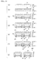
- FIG. 11 is a cross-sectional process drawing that describes the method of manufacturing the semiconductor package 20B that is provided with the penetration electrode 28 and the solder bump 29 in the second embodiment of the present invention.
- the filter 26 is formed on the other surface 24b of the cap substrate 24 as shown in (a) of FIG. 11 .
- the method of forming the filter 26 is the same as (a) of FIG. 10 .
- the cap substrate 24 in (a) of FIG. 11 is an aggregate 24' of the cap substrate 24 of the semiconductor package 20B).
- a protective film 50 is formed so as to cover the filter 26.
- this protective film 50 it is preferably one that can be removed in a subsequent step, and is preferably one that uses a resin that can be removed or a fine adhesion film.
- a spin coat of resin that can be removed, or a laminate of dry film (fine adhesion film or the like) is used.
- the cap substrate 24, the spacer 25, and the semiconductor substrate 22 are joined as shown in (c) of FIG. 11 .
- the semiconductor substrate 22 in (c) of FIG. 11 is an aggregate 22' of the semiconductor substrate 22 of the semiconductor package 20B).
- the penetration electrode 28 is formed from the other surface 22b of the semiconductor substrate 22 toward the electrode 27. In relation to the formation of the penetration electrode 28, it is the same as (c) of FIG. 10 .
- solder bump 29 is formed similarly to (d) of FIG. 10 so as to be electrically connected to the penetration electrode 28.
- the protective film 50 that was formed in (b) of FIG. 11 is removed.
- a chemical or dry process is used so as not to impart damage to the filter 26.
- O 2 ashing it is preferable to use O 2 ashing.
- the semiconductor package 20B of the present embodiment is obtained as shown in (g) of FIG. 11
- the manufacturing method of the present embodiment it is possible to prevent exfoliation of the filter 26 by the same reason as the first embodiment of FIG. 10 provided with the penetration electrodes 28 and the solder bumps 29. Also, since the filter 26 that is formed on the other surface 24b of the cap substrate 24 is covered by the protective film 50 after formation of the filter 26, it is possible to prevent damage to the filter 26 during the manufacturing process. Also, in relation to the penetration electrodes 28, since the opening location is not disposed at the dicing location, it is possible to prevent entry of particles or the like and deformation or the like due to dicing.
- FIG. 12 is a cross-sectional process drawing that describes the method of manufacturing the semiconductor package 30B according to the third embodiment that is provided with the penetration electrodes and the solder bumps.
- first the first filter 36a and the second filter 36b are formed on the surface 34a of the cap substrate 34 and the other surface 34b of the cap substrate 34, respectively, as shown in (a) of FIG. 12 .
- the cap substrate 34 in (a) of FIG. 12 is an aggregate 34' of the cap substrate 34 of the semiconductor package 30B).
- the method of forming the first filter 36a and the second filter 36b is the same as the manufacturing process of FIG. 10 .
- the second filter 36b is covered with a protective film 50.
- a protective film 50 In relation to the method of forming the protective film 50, it is the same as the manufacturing process of (b) of FIG. 11 .
- the cap substrate 34, the spacer 35, and the semiconductor substrate 32 are joined as shown in (c) of FIG. 12 .
- the semiconductor substrate 32 in (c) of FIG. 12 is an aggregate 32' of the semiconductor substrate 32 of the semiconductor package 30B).
- the penetration electrode 38 is formed from the other surface 32b of the semiconductor substrate 32 toward the electrode 37. In relation to the formation of the penetration electrode 38, it is the same as (c) of FIG. 10 .
- solder bump 39 is formed similarly to (d) of FIG. 10 so as to be electrically connected to the penetration electrode 38.
- the semiconductor package 30B of the present embodiment is obtained as shown in (g) of FIG. 12 .
- the present embodiment it is possible to prevent exfoliation of the first filter 36a and the second filter 36b by the same reason as the manufacturing steps of FIG. 11 and FIG. 12 . Also, in relation to the first filter 36a, since the filter is formed in the semiconductor package 30B, and also in relation to the second filter 36b since it is provided with a step of covering with the protective film 50 similarly to the second embodiment, it is possible to prevent damage to both filters during the manufacturing process. Also, in relation to the penetration electrode 38, since the opening location is not disposed on the dicing location, it is possible to prevent entry of particles or the like and deformation or the like due to dicing.
- one that is provided with the projecting portion 14P on the cap substrate 14 as shown in Examples 1 and 4 may be used.
- the spacer 15 being formed from resin, since the moisture permeability coefficient of resin is high, when the closure thickness of the resin is thick, there is a possibility of condensation forming in the gap 13. Also, if the distance from the semiconductor substrate 12 to the cap substrate 14 is short, optical problems related to such as imaging characteristics will arise.
- the cap substrate 14 By providing the cap substrate 14 with the projecting portion 14P in order to deal with both of these, thinning of the resin layer with a high moisture permeability coefficient is achieved and the condensation is suppressed, and by controlling the projecting portion 14P on the cap substrate 14, it is possible to adjust the distance from the semiconductor substrate 12 to the cap substrate 14.
- the height of the spacer 15 that joins the semiconductor substrate 12 and the projecting portion 14P on the cap substrate 14 is preferably 0.5 to 3 ⁇ m.
- the distance from the semiconductor substrate 12 to the cap substrate 14 is preferably 10 to 100 ⁇ m.
- the present invention is particularly useful in the case of disposing a filter on a cap substrate in packaging on a wafer level of a semiconductor device that is formed on a semiconductor substrate.
Landscapes
- Solid State Image Pick-Up Elements (AREA)
Abstract
Description
- The present invention relates to a semiconductor package and a manufacturing method thereof, and more specifically, to a countermeasure against exfoliation of a filter that is disposed in the semiconductor package.
- Priority is claimed on Japanese Patent Application No.
2007-171915, filed June 29, 2007 - For recent mobile phones and mobile information terminals, and mobile electronic devices such as digital cameras, their portability and weight saving are major market needs. For that reason, further reductions in the size and thickness of chips such as semiconductor integrated circuits that mounted therein are essential, and a stable manufacturing process is called for.
- In optical semiconductor devices that are represented by CCDs and CMOSs that are mounted in these mobile electronic devices, optical filters, such as an infrared cut-off filter, are used. When applying these optical filters to a wafer level package of an optical semiconductor, package processing may be performed that consists of forming an optical filter on a glass substrate.
- As procedures of forming a filter on a conventional glass substrate, there is a method that forms a filter on a glass substrate after the completion of package processing, and there is a method that first forms a filter on a glass substrate and then performs package processing. In the case of forming a filter in the interior of a package in order to protect the filter, the latter method is adopted. Also, although the former involves separately forming a filter in each package, that latter has the advantage of being able to form a filter at the wafer level at once.
-
FIG. 13 is a cross-sectional view of a manufacturing process for a conventional semiconductor package in which a filter is formed in a package. In the manufacturing process for thissemiconductor package 40, as shown in (a) ofFIG. 13 , thefilter 46 is disposed on asurface 44a of acap substrate 44. Next, thefilter 46 and asemiconductor substrate 42 are joined via aspacer 45. Next, as shown in (b) ofFIG. 13 , dicing of the semiconductor wafer is carried out at the location shown by the dashed line L. In the chipping due to this dicing, there is the possibility of exfoliation of thisfilter 46 occurring as shown in (d) ofFIG. 13 . Thisexfoliation 60 of thefilter 46 is magnified in a reliability test and the like, and at times it has caused thesemiconductor package 40 to malfunction. Also, since thespacer 45 is directly adhered to thefilter 46, when the adhesion between of thefilter 46 and thecap substrate 44 is weak, there is the possibility of thefilter 46 exfoliating under the stress arising from expansion and contraction of thespacer 45. - The present invention was achieved in view of the above circumstances, and has as its first object to provide a semiconductor package that is capable of suppressing exfoliation of a filter due to chipping in the dicing process. Also, the present invention has as its second object to provide a method of manufacturing a semiconductor package that is capable of suppressing exfoliation of a filter in the dicing process.
- A first aspect of the semiconductor package of the present invention is a semiconductor package that includes a semiconductor substrate having a semiconductor device disposed on one surface thereof, a cap substrate having one surface arranged opposite to the semiconductor substrate via a gap from the one surface of the semiconductor substrate, with the one surface provided with a flat portion over the entire area or a regional projecting portion along with the flat portion, and a spacer that is provided in a protruding manner at the flat portion or projecting portion of the one surface of the cap substrate opposite to the semiconductor substrate and that bonds the cap substrate and the semiconductor substrate, being provided with a filter that is disposed on the cap substrate, and the filter being at a position that overlaps with the semiconductor device and not overlapping with the spacer.
- In a second aspect of the semiconductor package of the present invention, the filter in the first aspect is disposed overlapping in the order of the semiconductor substrate, the filter, and the cap substrate.
- In a third aspect of the semiconductor package of the present invention, the filter in the first aspect is disposed overlapping in the order of the semiconductor substrate, the cap substrate, and the filter.
- In a fourth aspect of the semiconductor package of the present invention, the filter in the first aspect has a first filter and a second filter, and being disposed overlapping in the order of the semiconductor substrate, the first filter, the cap substrate, and the second filter.
- A fifth aspect of the semiconductor package of the present invention includes an electrode that is on one surface side of the semiconductor substrate and in electrical contact with the semiconductor device, a penetration electrode that is provided from the other surface side of the semiconductor substrate toward the electrode, and a solder bump that is electrically connected with the penetration electrode.
- A first aspect of a method of manufacturing a semiconductor package of the present invention is a method of manufacturing a semiconductor package that includes a semiconductor substrate having a semiconductor device disposed on one surface thereof, a cap substrate having one surface arranged opposite to the semiconductor substrate via a gap from the one surface of the semiconductor substrate, with the one surface provided with a flat portion over the entire area or a regional projecting portion along with the flat portion, and a spacer that is provided in a protruding manner at the flat portion or projecting portion of the one surface of the cap substrate opposite to the semiconductor substrate and that bonds the cap substrate and the semiconductor substrate, being provided with a filter that is disposed on the cap substrate, and the filter being at a position that overlaps with the semiconductor device without overlapping with the spacer, the method includes in the following order a first step that forms the filter on the cap substrate, a second step that bonds the semiconductor substrate on one surface of which a plurality of the semiconductor devices are disposed so as to mutually sandwich a dividing portion and the cap substrate on which the filter is disposed via the spacer at the separating portion, and a third step that divides a structure that includes the cap substrate, the semiconductor devices, the semiconductor substrate, and the spacer in the direction in which the semiconductor substrate and the cap substrate overlap at the region where the spacer is.
- A second aspect of the method of manufacturing a semiconductor package of the present invention includes, after the second step, a step that forms a penetration electrode to be electrically connected from the other surface side of the semiconductor substrate toward the semiconductor device and a step that forms a solder bump that is electrically connected with the penetration electrode.
- In a semiconductor package of the present invention, a cap substrate is arranged via a gap opposite from one surface of a semiconductor substrate in which a semiconductor device is disposed on one surface. A spacer is provided in a protruding manner on a surface of this cap substrate opposite to the semiconductor substrate and bonds the semiconductor substrate and the cap substrate. Also, a filter is disposed on the cap substrate so as to overlap with the semiconductor device, and is at a position that does not overlap with the spacer.
- With this constitution, since the division location of the semiconductor package is at a position that divides the spacer into two, it is possible to prevent exfoliation of the filter due to chipping without dividing the filter.
- Also, in a method of manufacturing a semiconductor package of the present invention, after forming the filter on the one surface of the cap substrate so as to overlap the semiconductor device, the spacer which is located in a position that does not overlap the filter brings into opposition and bonds the semiconductor substrate on which a plurality of semiconductor devices are disposed by providing a dividing portion and the cap substrate. Thereafter, a structure that is formed by the semiconductor substrate, the cap substrate, and the spacer being bonded is divided at a location that divides the spacer into two. In this manufacturing process, since the filter is not disposed at the place of division of the semiconductor package, in the division step, it is possible to prevent exfoliation of the filter from the cap substrate due to chipping.
-
-
FIG. 1 is a cross-sectional view of the semiconductor package that shows an example according to a first embodiment of the present invention. -
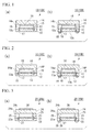
FIG. 2 is a cross-sectional view of a semiconductor package that shows an example according to Example 1 of the present invention. -
FIG. 3 is a cross-sectional view of a semiconductor package that shows an example according to a second embodiment of the present invention. -
FIG. 4 is a cross-sectional view of a semiconductor package that shows an example according to Example 2 of the present invention. -
FIG. 5 is a cross-sectional view of a semiconductor package that shows an example according to a third embodiment of the present invention. -
FIG. 6 is a cross-sectional view of a semiconductor package that shows an example according to Example 3 of the present invention. -
FIG. 7 is a cross-sectional process drawing of a semiconductor package according to a first embodiment of the present invention. -
FIG. 8 is a cross-sectional process drawing of a semiconductor package according to a second embodiment of the present invention. -
FIG. 9 is a cross-sectional process drawing of a semiconductor package according to a third embodiment of the present invention. -
FIG. 10 is a cross-sectional process drawing of a semiconductor package that is provided with a penetration electrode and a solder bump in the first embodiment of the present invention. -
FIG. 11 is a cross-sectional process drawing of the semiconductor package that is provided with a penetration electrode and a solder bump in the second embodiment of the present invention. -
FIG. 12 is a cross-sectional process drawing of the semiconductor package that is provided with a penetration electrode and a solder bump in the third embodiment of the present invention. -
FIG. 13 is a drawing of a conventional semiconductor package and a cross-sectional process drawing, and a schematic drawing of filter exfoliation. -
- 11, 21, 31, 41 semiconductor device
- 12, 22, 32, 42 semiconductor substrate
- 13, 23, 33, 43 gap
- 14, 24, 34, 44 cap substrate
- 14P, 24P, 34P, 44P cap substrate projecting portion
- 15, 25, 35, 45 spacer
- 16, 26, 36, (36a, 36b), 46 filter
- 17, 27, 37, 47 electrode
- 18, 28, 38 penetration electrode
- 19, 29, 39 solder bump
- 10 (10A, 10B, 10C, 10D) semiconductor package according to first embodiment
- 20 (20A, 20B, 20C, 20D) semiconductor package according to second embodiment
- 30 (30A, 30B, 30C, 30D) semiconductor package according to third embodiment
- 40 conventional semiconductor package
- 50 protective film
- 60 exfoliation of filter
- L dicing location
- Hereinbelow, the present invention shall be described with reference to the drawings.
- The present invention is not restricted by these embodiments.
-
FIG. 1 is a cross-sectional view that shows the first embodiment of the semi-conductor package according to the present invention. - In the
semiconductor package 10A, asemiconductor device 11 is disposed on asurface 12a of asemiconductor substrate 12. From thissemiconductor substrate 12, acap substrate 14 is disposed opposite via agap 13. Also, aspacer 15 is provided in a protruding manner on asurface 14a opposite to thesemiconductor substrate 12, and bonds thesemiconductor substrate 12 and thecap substrate 14. Furthermore, afilter 16 is disposed on thesurface 14a of thecap substrate 14 so as to overlap with thesemiconductor device 11 but not to overlap with thespacer 15. - In relation to the
semiconductor device 11, an image sensor such as a CCD or CMOS is preferred. Moreover, a MEMS (Micro Electro Mechanical System) device or the like can be used, with examples including a micro relay, a microswitch, a pressure sensor, an acceleration sensor, a high-frequency filter, a micro mirror, and the like. - As the material of the
semiconductor substrate 12, for example, gallium arsenide, glass, ceramic, germanium, silicon, and the like are used. Moreover, it is preferable to have anelectrode 17 that is in electrical contact with thesemiconductor device 11 disposed on thesurface 12a of thesemiconductor substrate 12. In relation to thiselectrode 17, provided it is in electrical contact with thesemiconductor device 11, it is not particularly limited, but the arrangement location is preferably provided on thesurface 12a of the semiconductor substrate. Concerning the material of theelectrode 17, Al, Al-Cu, Al-Si-Cu or the like is used. This is used as an I/O pad. - In relation to the
gap 13, it is not particularly limited, and can be freely selected corresponding to conditions such as the specification demanded from thesemiconductor device 11 or the like, and for example provided it is in the range of several µm to several hundred µm, it is possible to ensure a sufficient cavity in the vicinity of thesemiconductor device 11, and it is possible to control the dimensions of thesemiconductor package 10. - For example, in the case of the
semiconductor device 11 being an image sensor, such as a CCD, a CMOS, or the like, when the distance between thesemiconductor substrate 12 and thecap substrate 14 becomes too close, it may be susceptible to particles adhering to thecap substrate 14 and the like, and in such a case, it is possible to utilize to the upmost the role of thegap 13 that is secured between thesemiconductor substrate 12 and thecap substrate 14 by thespacer 15. - In relation to the
cap substrate 14, it is arranged above thesemiconductor device 11 via thegap 13, and has a role of protecting thesemiconductor device 11 or the like. As the material of thecap substrate 14, it is possible to use a plate that consists of resin or glass, metal or the like, and in the case of applying to an optical semiconductor device such as a CCD, a CMOS, or the like, it is preferable to use a material such as glass or the like that has light transmittance. Also, it is preferably parallel to and opposite to thesemiconductor substrate 12. - In order that the
spacer 15 may secure thegap 13 between thesemiconductor substrate 12 and thecap substrate 14, when joining thecap substrate 14 and thesemiconductor substrate 12, it is provided at a predetermined position so as to enclose the periphery of thesemiconductor device 11 without a break and not to cover the top of thesemiconductor device 11. Thereby, thegap 13 around thesemiconductor device 11 is hermetically sealed by thesemiconductor substrate 12, thecap substrate 14, and thespacer 15. Materials used for thespacer 15 include, for example, varnish or paint, dry film or the like consisting of photosensitive or non-photosensitive resin (UV curing resin, visible-light curing resin, infrared-light curing resin, thermosetting resin, etc.). - As the material suited to constituting the
spacer 15, a suitable selection should be made in accordance with the usage environment of the semiconductor package, but in particular a resin with excellent chemical resistance and thermal resistance, such as a polyimide or phenol resin, is suitable. In the case of a polyimide resin, by calcinating after forming the layer to cause a crosslinking reaction, it is possible to improve the chemical resistance and thermal resistance. - In the case of the material that constitutes the
spacer 15 having photosensitivity, the photosensitive material includes a photosensitive resin such as epoxy acrylate and a photosensitive glass paste and the like. - When calcinating polyimide resin or glass paste, by forming the
spacer 15 on thecap substrate 14 side and performing calcination of thespacer 15 prior to joining of thecap substrate 14 to thesemiconductor substrate 12, it is possible to avoid damage of thesemiconductor device 11 by the heat of the calcination. - Moreover, it is possible to hermetically seal the semiconductor package by making the spacer from a metal bond such as Sn or Au, glass, Si, and the like. Thereby, it is possible to prevent dew condensation in the
gap 13. - In relation to the
filter 16, the type of thefilter 16 to be used is not limited, and a notch filter or ND filter, a band pass filter, and the like can be freely selected depending on the use of thesemiconductor device 11. When using a CCD or a CMOS as the semiconductor device, it is preferable to use primary color filters that consist of red, green, and blue, complementary color filters that consist of cyan, magenta, yellow, and green, and an IR cut-off filter, etc. - In the present invention, the
filter 16 is disposed on thesurface 14a side of thecap substrate 14 at a position that overlaps thesemiconductor device 11. Thisfilter 16 may be directly disposed on thesurface 14a side of thecap substrate 14, and may be disposed via an object which is disposed on thesurface 14a side of thecap substrate 14. Also, since the position at which thisfilter 16 is arranged is a position that does not overlap with the dicing location and does not directly overlap with thespacer 15, it is possible to suppress exfoliation of thefilter 16 via chipping during dicing. Also, since thespacer 15 is not bonded to thefilter 16, it is possible to prevent exfoliation of thefilter 16 arising from expansion and contraction of thespacer 15. Moreover, since thefilter 16 is not disposed over the entire surface of thecap substrate 14, it is possible to relieve warping of thecap substrate 14 by the stress of thefilter 16. - As shown in
FIG. 3 , in the present invention, it is possible to arrange afilter 26 on another surface 24b of acap substrate 24. In this case as well, thefilter 26 may be directly disposed on theother surface 24b of thecap substrate 24, or thefilter 26 may be disposed via an object which is disposed on theother surface 24b of thecap substrate 24. Also, since the position at which thisfilter 26 is arranged does not overlap with the dicing location, it no longer becomes caught by the chipping during dicing. Moreover, since it is not in contact with aspacer 25, it is possible to avoid the exfoliation of thefilter 26 due to the stress of expansion and contraction of thespacer 25 as conventionally seen. Since thisfilter 26 is provided on the outer peripheral portion of thesemiconductor package 20, unnecessary light that directs thesemiconductor device 21 can be blocked before entering thesemiconductor package 20. - As shown in
FIG. 5 , in the present invention, it is possible to arrange a filter 36 on both onesurface 34a and theother surface 34b of a cap substrate. That is, asemiconductor substrate 32, afirst filter 36a, acap substrate 34, and asecond filter 36b are arranged in an overlapping manner in that order. In relation to the arrangement of thefirst filter 36a and thesecond filter 36b, they may be disposed directly on thecap substrate 34, and may be indirectly disposed via an object which is disposed on thecap substrate 34. In either case, since thefirst filter 36a and thesecond filter 36b are disposed at positions that do not overlap with thespacer 35 similarly to the two aforementioned embodiments, it is possible to prevent exfoliation of the filter due to chipping during dicing. Also, similarly to the aforementioned embodiments, since thespacer 35 is not directly bonded to bothfilters spacer 35. Moreover, in the case of disposing the filter 36 on both surfaces of thecap substrate 34, since stress of the filter 36 is applied to both surfaces of thecap substrate 34, it is possible to relieve warping of thecap substrate 34. In the case of an optical semiconductor device, by changing the combination of thefirst filter 36a and thesecond filter 36b, for example by changing the combination of an ND filter and a band pass filter, it is possible to manufacture anoptical semiconductor package 30 corresponding to various situations. - In the semiconductor package of the present invention, Example 1 of the first embodiment is shown in (a) of
FIG. 2 , and is provided with a projectingportion 14P on thecap substrate 14. In the case of thespacer 15 consisting of resin, since the moisture permeability coefficient of resin is high, when the closure thickness of the resin is thick, there is a possibility of condensation forming in thegap 13. Also, if the distance from thesemiconductor substrate 12 to thecap substrate 14 is short, optical problems related to such as imaging characteristics will arise. By equipping thecap substrate 14 with the projectingportion 14P in order to deal with both of these, thinning of the resin layer with a high moisture permeability coefficient is achieved and the condensation is suppressed, and by controlling the projectingportion 14P on thecap substrate 14, it is possible to adjust the distance from thesemiconductor substrate 12 to thecap substrate 14. At this time, the height of thespacer 15 that joins thesemiconductor substrate 12 and the projectingportion 14P on thecap substrate 14 is preferably 0.5 to 3 µm. Also, the distance from thesemiconductor substrate 12 to thecap substrate 14 is preferably 10 to 100 µm. - As Example 2 of the second embodiment of the present invention, as shown in (a) of
FIG. 4 , a projectingportion 24P is provided on thecap substrate 24. With this constitution, the same effect as Example 1 is obtained. - As Example 3 of the third embodiment of the present invention, as shown in (a) of
FIG. 6 , a projectingportion 34P is provided on thecap substrate 34. With this constitution, it is possible to obtain the same effect as Example 1 and Example 2. - Also, in the semiconductor package of the present invention, as shown in (b) of
FIG. 1 , it is possible to provide apenetration electrode 18 and asolder bump 19. Thepenetration electrode 18 is provided from theother surface 12b side of thesemiconductor substrate 12 toward theelectrode 17, and thesolder bump 19 is provided in electrical connection with thispenetration electrode 18. Also, as shown in (b) ofFIG. 3 and (b) ofFIG. 5 , it is possible to form thepenetration electrodes - In relation to the
penetration electrode 18, an electrically conducting path is formed that enables theelectrode 17 to conduct with the outside via the thoughelectrode 18. The shape of thepenetration electrode 18 is not particularly limited, but it is preferable to install it at a right angle to thesemiconductor device 11. Also, as the material thereof, it is preferable to use metal, such as tin or copper. It is possible to form a back wiring layer on theother surface 12b of thesemiconductor substrate 12 so as to make contact with thispenetration electrode 18. - In relation to the
solder bump 19, it is formed on theother surface 12b of the semiconductor substrate where thepenetration electrode 18 is disposed, and installed so as to be in electrical contact with thepenetration electrode 18. In relation to the material of thesolder bump 19, the solder alloy that is used is not particularly limited, but in the case of using a lead-free solder alloy, it is preferable to use Sn Ag 3.0 Cu 0.5 or Sn Ag 3.5 Cu 0.7, and more preferable to use Sn Ag 3.0 Cu 0.5. Also, the size of thesolder bump 19 and the pitch of forming thesolder bump 19 are not particularly limited, but it is preferable for the size to be 30 to 250 µm and the pitch to be 100 to 400 µm. - By providing the
penetration electrode 18 and thesolder bump 19, compared to a conventional wire bonding, an improvement in the signal speed is achieved. - Also in the semiconductor package that is provided with the penetration electrode and the solder bump in the first embodiment of the present invention, as the Example 4, it is possible to use one that is similarly provided with a projecting
portion 14P on the cap substrate. In the case of thespacer 15 being formed from resin, since the moisture permeability coefficient of resin is high, when the closure thickness of the resin is thick, there is a possibility of condensation forming in thegap 13. Also, if the distance from thesemiconductor substrate 12 to thecap substrate 14 is short, optical problems related to such as imaging characteristics will arise. By providing thecap substrate 14 with the projectingportion 14P in order to deal with both of these, the resin layer with a high moisture permeability coefficient is thinned and the condensation is suppressed, and by controlling the projectingportion 14P on thecap substrate 14, it is possible to adjust the distance from thesemiconductor substrate 12 to thecap substrate 14. At this time, the height of thespacer 15 that joins thesemiconductor substrate 12 and the projectingportion 14P on thecap substrate 14 is preferably 0.5 to 3 µm. Also, the distance from thesemiconductor substrate 12 to thecap substrate 14 is preferably 10 to 100 µm. - Also in the semiconductor package that provides the penetration electrode and the solder bump in the second embodiment of the present invention, there is an Example 5 in which the projecting
portion 24P is installed on thecap substrate 24 as shown in (b) ofFIG. 4 . With this constitution, the same effect as Example 4 is obtained. - Also in the semiconductor package that provides the penetration electrode and the solder bump in the third embodiment of the present invention, there is an Example 6 in which the projecting
portion 34P is installed on thecap substrate 34 as shown in (b) ofFIG. 6 . With this constitution, the same effect as Example 4 and Example 5 is obtained. - In the method of manufacturing the
semiconductor package 10A of the first embodiment, first thefilter 16 is formed on thesurface 14a of thecap substrate 14 as shown in (a) ofFIG. 7 . (Here, thecap substrate 14 in (a) ofFIG. 7 is an aggregate 14' of thecap substrate 14 of thesemiconductor package 10A). As one example of this method of forming thefilter 16 on thecap substrate 14, after forming a photosensitive resin on thesurface 14a of thecap substrate 14 using a spin coater or the like, a pattern in accordance with the use condition is formed by technique of photolithography. As the material of the photosensitive resin, it is preferable to use a photopolymerization-type acrylic resin or one based on photo-crosslinkable polyvinyl alcohol. Also, when forming a color filter, it is possible to form it by an etching method with a polyimide precursor that is dispersed with a pigment serving as a colored resin layer. Also, there are some that consist of laminating TiO2, SiO2, MgF2, Ta2O5 and the like by vapor deposition. - Next, as shown in (b) of
FIG. 7 , thespacer 15 is formed so as to be installed in a projecting manner on thecap substrate 14a, and the semiconductor substrate 12' on which thesemiconductor device 11 and theelectrode 17 are disposed is bonded. (Here, thesemiconductor substrate 12 in (b) ofFIG. 7 is an aggregate 12' of thesemiconductor substrate 12 of thesemiconductor package 10A). Thecap substrate 14 is made to face the semiconductor substrate 12', and thespacer 15 that is formed on thesurface 14a of thecap substrate 14 is bonded to thesurface 12a of thesemiconductor substrate 12. Thereby, thesemiconductor substrate 12 and thecap substrate 14 are joined via thespacer 15. It is preferable to join them using an epoxy resin or a photosensitive BCB resin or the like. - Next, if the
semiconductor substrate 12, thespacer 15, and thecap substrate 14 are divided by a dicing saw or the like along the cutting line L shown in (b) ofFIG. 7 so that thespacer 15 is cut in two, thesemiconductor package 10A of the present embodiment is obtained as shown in (c) ofFIG. 7 . - According to the manufacturing method of the
semiconductor package 10A of the present invention, since thefilter 16 is formed on a portion of thesurface 14a of thecap substrate 14 without being formed on the entire surface thereof, it is possible to relieve warping of thecap substrate 14 by the stress of thefilter 16. Also, thefilter 16 is not installed on the dicing location L; it is possible to prevent exfoliation of thefilter 16 by chipping due to dicing. Furthermore, since thefilter 16 is not caught by thespacer 15 and thecap substrate 14, it is possible to also prevent thefilter 16 from exfoliating by the stress arising from the expansion and contraction of thespacer 15. Also, since thefilter 16 is formed inside of thesemiconductor package 10A, thefilter 16 is protected during the processing of thesemiconductor package 10A. - Next,
FIG. 8 is a cross-sectional process drawing that describes the method of manufacturing thesemiconductor package 20A according to the second embodiment of the present invention. - In the second embodiment of the present invention, explanations that overlap with the first embodiment shall be omitted.
- In the manufacturing method in the second embodiment, first the
filter 26 is formed on theother surface 24b of thecap substrate 24, as shown in (a) ofFIG. 8 . (Here, thecap substrate 24 in (a) ofFIG. 8 is an aggregate 24' of thecap substrate 24 of thesemiconductor package 20A). The method of forming thefilter 26 is the same as that of the first embodiment. - Next, as shown in (b) of
FIG. 8 , aprotective film 50 is formed so as to cover thefilter 26. In relation to thisprotective film 50, it is preferably one that can be removed in a subsequent step, and is preferably one that uses a resin that can be removed or a fine adhesion film. In relation to the method of forming thisprotective film 50, a laminate of film, a spin coat of resin that can be removed, or the like, is used. - Next, similarly to (b) of
FIG. 7 of the first embodiment, thecap substrate 24, thespacer 25, and thesemiconductor substrate 22 are joined as shown in (c) ofFIG. 8 . (Here, thesemiconductor substrate 22 in (c) ofFIG. 8 is an aggregate 22' of thesemiconductor substrate 22 of thesemiconductor package 20A). - Next, as shown in (d) of
FIG. 8 , theprotective film 50 that was formed in (b) ofFIG. 8 is removed. In relation to the removal of theprotective film 50, a chemical (or in the case of film a separator) is used so as not to damage thefilter 26. Also, it is preferable to remove theprotective film 50 by performing a dry process such as O2 ashing. - Next, if the
semiconductor substrate 22, thespacer 25, and thecap substrate 24 are divided along the cutting line L shown in (d) ofFIG. 8 , thesemiconductor package 20A of the present embodiment is obtained as shown in (e) ofFIG. 8 . - According to the manufacturing method of the
semiconductor package 20A of the second embodiment of the present invention, it is possible to prevent exfoliation of thefilter 26 by the same reason as the first embodiment. Also, since thefilter 26 that is formed on theother surface 24b of thecap substrate 24 is covered by theprotective film 50 after formation of thefilter 26, it is possible to prevent damage to thefilter 26 during the manufacturing process. - Next,
FIG. 9 is a cross-sectional process drawing that describes the method of manufacturing thesemiconductor package 30A according to the third embodiment. In the third embodiment of the present invention, explanations that overlap with the first embodiment and the second embodiment shall be omitted. - In the method of manufacture in the third embodiment, first the
first filter 36a and thesecond filter 36b are formed on thesurface 34a of thecap substrate 34 and theother surface 34b of thecap substrate 34, respectively, as shown in (a) ofFIG. 9 . (Here, thecap substrate 34 in (a) ofFIG. 9 is an aggregate 34' of thecap substrate 34 of thesemiconductor package 30A). The method of forming thefirst filter 36a and thesecond filter 36b is the same as that of the first embodiment and the second embodiment. - Next, as shown in (b) of
FIG. 9 , thesecond filter 36b is covered with aprotective film 50. In relation to the method of forming theprotective film 50, it is the same as the case of the second embodiment. - Next, similarly to (b) of
FIG. 7 of the first embodiment, thecap substrate 34, thespacer 35, and thesemiconductor substrate 32 are joined as shown in (c) ofFIG. 9 . (Here, thesemiconductor substrate 32 in (c) ofFIG. 9 is an aggregate 32' of thesemiconductor substrate 32 of thesemiconductor package 30A). - Next, as shown in (d) of
FIG. 9 , theprotective film 50 that was formed in (b) ofFIG. 9 is removed. This step is the same as the method shown in (d) ofFIG. 8 of the second embodiment. - Finally, if the
semiconductor substrate 32, thespacer 35, and thecap substrate 34 are divided along the cutting line L shown in (d) ofFIG. 9 , thesemiconductor package 30A of the present embodiment is obtained as shown in (e) ofFIG. 9 . - In the third embodiment as well, it is possible to prevent exfoliation of the
first filter 36a and thesecond filter 36b for the same reason as the first embodiment and the second embodiment. Also, in relation to thefirst filter 36a, since the filter is formed in thesemiconductor package 30, and also in relation to thesecond filter 36b since it is provided with a step of covering with a protective film similarly to the second embodiment, it is possible to prevent damage to both filters during the manufacturing process. - Method of manufacturing a semiconductor package in which penetration electrodes and soldier bumps are formed
- In the method of manufacturing the
semiconductor package 10B of the first embodiment that is provided with penetration electrodes and solder bumps, first thefilter 16 is formed on thesurface 14a of thecap substrate 14 as shown in (a) ofFIG. 10 . (Here, thecap substrate 14 in (a) ofFIG. 10 is an aggregate 14' of thecap substrate 14 of thesemiconductor package 10B). As one example of this method of forming thefilter 16 on thecap substrate 14, after forming a photosensitive resin on thesurface 14a of thecap substrate 14 using a spin coater or the like, a pattern in accordance with the use condition is formed by technique of photolithography. As the material of the photosensitive resin, it is preferable to use a photopolymerization-type acrylic resin or one based on photo-crosslinkable polyvinyl alcohol. Also, when forming a color filter, it is possible to form it by an etching method with a polyimide precursor that is dispersed with a pigment serving as a colored resin layer. - Next, as shown in (b) of
FIG. 10 , thespacer 15 is formed so as to be installed in a projecting manner on thecap substrate 14a, and thesemiconductor substrate 12 on which thesemiconductor device 11 and theelectrode 17 are disposed is bonded. (Here, thesemiconductor substrate 12 in (b) ofFIG. 10 is an aggregate 12' of thesemiconductor substrate 12 of thesemiconductor package 10B). - The
cap substrate 14 is made to face thesemiconductor substrate 12, and thespacer 15 that is formed on thesurface 14a of thecap substrate 14 is bonded to thesurface 12a of thesemiconductor substrate 12. Thereby, thesemiconductor substrate 12 and thecap substrate 14 are joined via thespacer 15. It is preferable to join them using an epoxy resin or a photosensitive BCB resin or the like. - Next, as shown in (c) of
FIG. 10 , through holes are formed from theother surface 12b of thesemiconductor substrate 12 toward theelectrode 17. In relation to the formation of the through holes, it is preferable to use a silicon deep etching apparatus (DeepRIE). An SiO2 layer is formed in each through hole as an oxide film layer using plasma-enhanced chemical vapor deposition to form an insulative layer in each through hole. Next, using reactive ion etching, the SiO2 layer of the hole bottom portion is selectively removed. Thereafter, a seed layer is formed by sputtering, and thepenetration electrode 18 and, although not shown in the drawing, where necessary a back wiring layer are formed by electrolytic plating. - Next, as shown in (d) of
FIG. 10 , the solder bumps 19 are formed so as to be electrically connected to thepenetration electrodes 18. In relation to the formation of the solder bumps 19, it is preferable to perform a HASL process, OSP process, electroless Ni-immersion Au process, or immersion Ag process, or the like, according to necessity. Also, although not shown in the drawing, in the case of manufacturing a back wiring layer, the solder bumps 19 are manufactured so as to be electrically connected to the back wiring layer. - Next, if the
semiconductor substrate 12 and thecap substrate 14 are divided along the cutting line L shown in (d) ofFIG. 10 so that thespacer 15 is cut in two, thesemiconductor package 10B that is provided with thepenetration electrodes 18 and the solder bumps 19 is obtained as shown in (e) ofFIG. 10 . - According to the manufacturing method of the
semiconductor package 10B of the present invention, since thefilter 16 is not installed on the dicing location L, it is possible to prevent exfoliation of thefilter 16 by chipping due to dicing. Furthermore, since thefilter 16 is formed on a portion of thesurface 14a of thecap substrate 14 without being formed on the entire surface thereof, it is possible to relieve warping of thecap substrate 14 by the stress of thefilter 16. Furthermore, since thefilter 16 is not caught by thespacer 15 and thecap substrate 14, it is possible to also prevent thefilter 16 from exfoliating by the stress arising from the expansion and contraction of thespacer 15. In addition, since thefilter 16 is formed inside of thesemiconductor package 10B, thefilter 16 is protected during the processing of thesemiconductor package 10B. In relation to thepenetration electrode 18, since the opening location is not disposed on the dicing location, it is possible to prevent entry of particles or the like and deformation and the like due to dicing. - Next,
FIG. 11 is a cross-sectional process drawing that describes the method of manufacturing thesemiconductor package 20B that is provided with thepenetration electrode 28 and thesolder bump 29 in the second embodiment of the present invention. - In the second embodiment of the present invention that is provided with the
penetration electrode 28 and thesolder bump 29, descriptions that overlap with the manufacturing process ofFIG. 10 shall be omitted. - In the manufacturing method in the present embodiment, first the
filter 26 is formed on theother surface 24b of thecap substrate 24 as shown in (a) ofFIG. 11 . The method of forming thefilter 26 is the same as (a) ofFIG. 10 . (Here, thecap substrate 24 in (a) ofFIG. 11 is an aggregate 24' of thecap substrate 24 of thesemiconductor package 20B). - Next, as shown in (b) of
FIG. 11 , aprotective film 50 is formed so as to cover thefilter 26. - In relation to this
protective film 50, it is preferably one that can be removed in a subsequent step, and is preferably one that uses a resin that can be removed or a fine adhesion film. In relation to the method of forming thisprotective film 50, a spin coat of resin that can be removed, or a laminate of dry film (fine adhesion film or the like) is used. - Next, similarly to (b) of
FIG. 10 , thecap substrate 24, thespacer 25, and thesemiconductor substrate 22 are joined as shown in (c) ofFIG. 11 . (Here, thesemiconductor substrate 22 in (c) ofFIG. 11 is an aggregate 22' of thesemiconductor substrate 22 of thesemiconductor package 20B). - Next, as shown in (d) of
FIG. 11 , thepenetration electrode 28 is formed from theother surface 22b of thesemiconductor substrate 22 toward theelectrode 27. In relation to the formation of thepenetration electrode 28, it is the same as (c) ofFIG. 10 . - Next, as shown in (e) of
FIG. 11 , thesolder bump 29 is formed similarly to (d) ofFIG. 10 so as to be electrically connected to thepenetration electrode 28. - Next, as shown in (f) of
FIG. 11 , theprotective film 50 that was formed in (b) ofFIG. 11 is removed. In relation to the removal of theprotective film 50, a chemical or dry process is used so as not to impart damage to thefilter 26. Also, in relation to the chemical, it is preferable to remove theprotective film 50 that is formed so as to cover thefilter 26 using an organic solvent such as acetone that does not cause damage to the filter. In the dry process, it is preferable to use O2 ashing. - Next, if the
semiconductor substrate 22, thespacer 25, and thecap substrate 24 are divided along the cutting line L shown in (f) ofFIG. 11 , thesemiconductor package 20B of the present embodiment is obtained as shown in (g) ofFIG. 11 - According to the manufacturing method of the present embodiment, it is possible to prevent exfoliation of the
filter 26 by the same reason as the first embodiment ofFIG. 10 provided with thepenetration electrodes 28 and the solder bumps 29. Also, since thefilter 26 that is formed on theother surface 24b of thecap substrate 24 is covered by theprotective film 50 after formation of thefilter 26, it is possible to prevent damage to thefilter 26 during the manufacturing process. Also, in relation to thepenetration electrodes 28, since the opening location is not disposed at the dicing location, it is possible to prevent entry of particles or the like and deformation or the like due to dicing. - Next,
FIG. 12 is a cross-sectional process drawing that describes the method of manufacturing thesemiconductor package 30B according to the third embodiment that is provided with the penetration electrodes and the solder bumps. - In the method of manufacture in the third embodiment, first the
first filter 36a and thesecond filter 36b are formed on thesurface 34a of thecap substrate 34 and theother surface 34b of thecap substrate 34, respectively, as shown in (a) ofFIG. 12 . (Here, thecap substrate 34 in (a) ofFIG. 12 is an aggregate 34' of thecap substrate 34 of thesemiconductor package 30B). The method of forming thefirst filter 36a and thesecond filter 36b is the same as the manufacturing process ofFIG. 10 . - Next, as shown in (b) of
FIG. 12 , thesecond filter 36b is covered with aprotective film 50. In relation to the method of forming theprotective film 50, it is the same as the manufacturing process of (b) ofFIG. 11 . - Next, similarly to (b) of
FIG. 10 , thecap substrate 34, thespacer 35, and thesemiconductor substrate 32 are joined as shown in (c) ofFIG. 12 . (Here, thesemiconductor substrate 32 in (c) ofFIG. 12 is an aggregate 32' of thesemiconductor substrate 32 of thesemiconductor package 30B). - Next, as shown in (d) of
FIG. 12 , thepenetration electrode 38 is formed from theother surface 32b of thesemiconductor substrate 32 toward theelectrode 37. In relation to the formation of thepenetration electrode 38, it is the same as (c) ofFIG. 10 . - Next, as shown in (e) of
FIG. 12 , thesolder bump 39 is formed similarly to (d) ofFIG. 10 so as to be electrically connected to thepenetration electrode 38. - Next, as shown in (f) of
FIG. 12 , theprotective film 50 that was formed in (b) ofFIG. 12 is removed. This step is the same as (f) ofFIG. 11 . - Next, if the
semiconductor substrate 32, thespacer 35, and thecap substrate 34 are divided along the cutting line L shown in (f) ofFIG. 12 , thesemiconductor package 30B of the present embodiment is obtained as shown in (g) ofFIG. 12 . - In the present embodiment, it is possible to prevent exfoliation of the
first filter 36a and thesecond filter 36b by the same reason as the manufacturing steps ofFIG. 11 andFIG. 12 . Also, in relation to thefirst filter 36a, since the filter is formed in thesemiconductor package 30B, and also in relation to thesecond filter 36b since it is provided with a step of covering with theprotective film 50 similarly to the second embodiment, it is possible to prevent damage to both filters during the manufacturing process. Also, in relation to thepenetration electrode 38, since the opening location is not disposed on the dicing location, it is possible to prevent entry of particles or the like and deformation or the like due to dicing. - Also, in the manufacturing process of the first embodiment, one that is provided with the projecting
portion 14P on thecap substrate 14 as shown in Examples 1 and 4 may be used. In the case of thespacer 15 being formed from resin, since the moisture permeability coefficient of resin is high, when the closure thickness of the resin is thick, there is a possibility of condensation forming in thegap 13. Also, if the distance from thesemiconductor substrate 12 to thecap substrate 14 is short, optical problems related to such as imaging characteristics will arise. By providing thecap substrate 14 with the projectingportion 14P in order to deal with both of these, thinning of the resin layer with a high moisture permeability coefficient is achieved and the condensation is suppressed, and by controlling the projectingportion 14P on thecap substrate 14, it is possible to adjust the distance from thesemiconductor substrate 12 to thecap substrate 14. At this time, the height of thespacer 15 that joins thesemiconductor substrate 12 and the projectingportion 14P on thecap substrate 14 is preferably 0.5 to 3 µm. Also, the distance from thesemiconductor substrate 12 to thecap substrate 14 is preferably 10 to 100 µm. - Also, by similarly providing the projecting portion on the cap substrate in the manufacturing process of the second embodiment and the manufacturing process of the third embodiment, it is possible to achieve the same effects as above.
- Furthermore, it is the same even in each manufacturing step of a semiconductor device that is provided with penetration electrodes and soldering bumps.
- The present invention is particularly useful in the case of disposing a filter on a cap substrate in packaging on a wafer level of a semiconductor device that is formed on a semiconductor substrate.
Claims (7)
- A semiconductor package comprising:a semiconductor device;a semiconductor substrate having the semiconductor device arranged on one surface;a cap substrate having one surface that opposes the one surface of the semiconductor substrate via a gap;a spacer that is arranged between the one surface of the semiconductor substrate and the one surface of the cap substrate, and that joins the semiconductor substrate and the cap substrate; anda filter that is provided on the cap substrate so as to overlap with the semiconductor device without overlapping with the spacer.
- The semiconductor package according to claim 1, wherein the filter is disposed overlapping in the order of the semiconductor substrate, the filter, and the cap substrate.
- The semiconductor package according to claim 1, wherein the filter is disposed overlapping in the order of the semiconductor substrate, the cap substrate, and the filter.
- The semiconductor package according to claim 1, wherein the filter includes a first filter and a second filter, and are disposed overlapping in the order of the semiconductor substrate, the first filter, the cap substrate, and the second filter.
- The semiconductor package according to claim 1, provided with:an electrode that is on the one surface side of the semiconductor substrate and in electrical contact with the semiconductor device;a penetration electrode that is provided from the other surface side of the semiconductor substrate toward the electrode; and a solder bump that is electrically connected with the penetration electrode.
- A method of manufacturing a semiconductor package provided with a semiconductor device; a semiconductor substrate having the semiconductor device arranged on one surface; a cap substrate having one surface that opposes the one surface of the semiconductor substrate via a gap; a spacer that is arranged between the one surface of the semiconductor substrate and the one surface of the cap substrate, and that joins the semiconductor substrate and the cap substrate; and a filter that is provided on the cap substrate so as to overlap with the semiconductor device without overlapping with the spacer,
the method provided with a first step that forms a plurality of the filters on the cap substrate; a second step that bonds the semiconductor substrate on one surface of which a plurality of the semiconductor devices are disposed so as to mutually sandwich a dividing portion and the cap substrate on which the plurality of filters are arranged via the spacer at the separating portion; and a third step that divides a structure that consists of the cap substrate, the plurality of semiconductor devices, the semiconductor substrate, and the spacer at an area where the spacer is in the direction in which the semiconductor substrate and the cap substrate overlap. - The method of manufacturing a semiconductor package according to claim 6 provided with, after the second step, a step that forms a penetration electrode to be electrically connected from the other surface side of the semiconductor substrate toward the semiconductor device and a step that forms a solder bump that is electrically connected with the penetration electrode.
Applications Claiming Priority (2)
| Application Number | Priority Date | Filing Date | Title |
|---|---|---|---|
| JP2007171915A JP2009010261A (en) | 2007-06-29 | 2007-06-29 | Semiconductor package and manufacturing method thereof |
| PCT/JP2008/061773 WO2009005017A1 (en) | 2007-06-29 | 2008-06-27 | Semiconductor package and method for manufacturing the same |
Publications (2)
| Publication Number | Publication Date |
|---|---|
| EP2164098A1 true EP2164098A1 (en) | 2010-03-17 |
| EP2164098A4 EP2164098A4 (en) | 2013-03-13 |
Family
ID=40226063
Family Applications (1)
| Application Number | Title | Priority Date | Filing Date |
|---|---|---|---|
| EP08790715A Withdrawn EP2164098A4 (en) | 2007-06-29 | 2008-06-27 | SEMICONDUCTOR HOUSING AND METHOD FOR MANUFACTURING THE SAME |
Country Status (7)
| Country | Link |
|---|---|
| US (1) | US8330268B2 (en) |
| EP (1) | EP2164098A4 (en) |
| JP (1) | JP2009010261A (en) |
| KR (1) | KR20100025538A (en) |
| CN (1) | CN101689533A (en) |
| TW (1) | TW200913239A (en) |
| WO (1) | WO2009005017A1 (en) |
Cited By (5)
| Publication number | Priority date | Publication date | Assignee | Title |
|---|---|---|---|---|
| EP2287910A1 (en) * | 2009-08-17 | 2011-02-23 | STMicroelectronics (Research & Development) Limited | Improvements in or relating to filters in an image sensor |
| WO2011035783A1 (en) * | 2009-09-24 | 2011-03-31 | Msg Lithoglas Ag | Method for producing a housing with a component in a hollow space, corresponding housing, method for producing a semi-finished product, and semi-finished product |
| WO2011156926A1 (en) * | 2010-06-14 | 2011-12-22 | Heptagon Oy | Method of manufacturing a plurality of optical devices |
| US9820637B2 (en) | 2012-09-24 | 2017-11-21 | Olympus Corporation | Image pickup apparatus and endoscope including image pickup apparatus |
| US12310132B2 (en) | 2019-05-15 | 2025-05-20 | Sony Semiconductor Solutions Corporation | Semiconductor package, semiconductor package manufacturing method, and electronic device |
Families Citing this family (13)
| Publication number | Priority date | Publication date | Assignee | Title |
|---|---|---|---|---|
| JPWO2010095201A1 (en) * | 2009-02-20 | 2012-08-16 | パナソニック株式会社 | Semiconductor device and manufacturing method of semiconductor device |
| US9075182B2 (en) | 2011-06-03 | 2015-07-07 | VisEra Technology Company Limited | Camera module and spacer of a lens structure in the camera module |
| KR101980657B1 (en) * | 2011-06-30 | 2019-05-22 | 엘지이노텍 주식회사 | The manufacturing method of lens assembly |
| KR101980634B1 (en) * | 2011-06-30 | 2019-05-22 | 엘지이노텍 주식회사 | Lens unit, and camera module having the same |
| JP5903796B2 (en) * | 2011-08-12 | 2016-04-13 | ソニー株式会社 | Imaging device and camera module |
| TWI462266B (en) * | 2012-03-20 | 2014-11-21 | 南茂科技股份有限公司 | Wafer stack structure and manufacturing method thereof |
| US9427776B2 (en) | 2012-08-23 | 2016-08-30 | Raytheon Company | Method of stress relief in anti-reflective coated cap wafers for wafer level packaged infrared focal plane arrays |
| JP6185813B2 (en) * | 2013-09-30 | 2017-08-23 | 三星ダイヤモンド工業株式会社 | Method and apparatus for dividing wafer laminate for image sensor |
| CN107110726A (en) * | 2014-12-24 | 2017-08-29 | 株式会社藤仓 | Pressure sensor and pressure sensor module |
| JP6054501B1 (en) * | 2015-12-17 | 2016-12-27 | 株式会社フジクラ | Termination device and termination method |
| US11174705B2 (en) | 2019-04-30 | 2021-11-16 | Weatherford Technology Holdings, Llc | Tubing tester valve and associated methods |
| TWI782830B (en) * | 2021-12-21 | 2022-11-01 | 勝麗國際股份有限公司 | Sensor package structure |
| US20260129987A1 (en) | 2024-11-06 | 2026-05-07 | Semiconductor Components Industries, Llc | Flare mitigating image sensor packages and related methods |
Family Cites Families (15)
| Publication number | Priority date | Publication date | Assignee | Title |
|---|---|---|---|---|
| JP2002373977A (en) * | 2001-06-14 | 2002-12-26 | Canon Inc | Solid-state imaging device |
| US7276798B2 (en) * | 2002-05-23 | 2007-10-02 | Honeywell International Inc. | Integral topside vacuum package |
| JP2005101911A (en) * | 2003-09-25 | 2005-04-14 | Konica Minolta Opto Inc | Imaging device and portable terminal |
| JP2005125447A (en) * | 2003-10-23 | 2005-05-19 | Hitachi Ltd | Electronic component and manufacturing method thereof |
| US7303645B2 (en) * | 2003-10-24 | 2007-12-04 | Miradia Inc. | Method and system for hermetically sealing packages for optics |
| JP2005136144A (en) * | 2003-10-30 | 2005-05-26 | Kyocera Corp | Solid-state imaging device |
| JP4761713B2 (en) * | 2004-01-28 | 2011-08-31 | 京セラ株式会社 | Electronic component sealing substrate, multi-component electronic component sealing substrate, and method of manufacturing electronic device |
| US8049806B2 (en) * | 2004-09-27 | 2011-11-01 | Digitaloptics Corporation East | Thin camera and associated methods |
| US7511262B2 (en) * | 2004-08-30 | 2009-03-31 | Micron Technology, Inc. | Optical device and assembly for use with imaging dies, and wafer-label imager assembly |
| JP4381274B2 (en) | 2004-10-04 | 2009-12-09 | シャープ株式会社 | Semiconductor device and manufacturing method thereof |
| JP2006173557A (en) * | 2004-11-22 | 2006-06-29 | Toshiba Corp | Hollow semiconductor device and manufacturing method thereof |
| US20060226452A1 (en) * | 2005-04-08 | 2006-10-12 | Konica Minolta Opto, Inc. | Solid-state image pickup device and the manufacture method thereof |
| JP4889974B2 (en) * | 2005-08-01 | 2012-03-07 | 新光電気工業株式会社 | Electronic component mounting structure and manufacturing method thereof |
| JP2007129164A (en) * | 2005-11-07 | 2007-05-24 | Sharp Corp | Optical device module, optical device module manufacturing method, and structure |
| JP2007171915A (en) | 2005-11-22 | 2007-07-05 | Ricoh Co Ltd | Image forming apparatus and image forming method |
-
2007
- 2007-06-29 JP JP2007171915A patent/JP2009010261A/en active Pending
-
2008
- 2008-06-27 CN CN200880022659A patent/CN101689533A/en active Pending
- 2008-06-27 WO PCT/JP2008/061773 patent/WO2009005017A1/en not_active Ceased
- 2008-06-27 KR KR1020097027099A patent/KR20100025538A/en not_active Withdrawn
- 2008-06-27 EP EP08790715A patent/EP2164098A4/en not_active Withdrawn
- 2008-06-30 TW TW097124527A patent/TW200913239A/en unknown
-
2009
- 2009-12-28 US US12/648,172 patent/US8330268B2/en not_active Expired - Fee Related
Cited By (6)
| Publication number | Priority date | Publication date | Assignee | Title |
|---|---|---|---|---|
| EP2287910A1 (en) * | 2009-08-17 | 2011-02-23 | STMicroelectronics (Research & Development) Limited | Improvements in or relating to filters in an image sensor |
| WO2011035783A1 (en) * | 2009-09-24 | 2011-03-31 | Msg Lithoglas Ag | Method for producing a housing with a component in a hollow space, corresponding housing, method for producing a semi-finished product, and semi-finished product |
| EP3297036A1 (en) * | 2009-09-24 | 2018-03-21 | MSG Lithoglas GmbH | Method for producing an assembly comprising a component on a carrier substrate and assembly and method for producing a semi-finished product |
| WO2011156926A1 (en) * | 2010-06-14 | 2011-12-22 | Heptagon Oy | Method of manufacturing a plurality of optical devices |
| US9820637B2 (en) | 2012-09-24 | 2017-11-21 | Olympus Corporation | Image pickup apparatus and endoscope including image pickup apparatus |
| US12310132B2 (en) | 2019-05-15 | 2025-05-20 | Sony Semiconductor Solutions Corporation | Semiconductor package, semiconductor package manufacturing method, and electronic device |
Also Published As
| Publication number | Publication date |
|---|---|
| JP2009010261A (en) | 2009-01-15 |
| US20100102437A1 (en) | 2010-04-29 |
| TW200913239A (en) | 2009-03-16 |
| KR20100025538A (en) | 2010-03-09 |
| CN101689533A (en) | 2010-03-31 |
| EP2164098A4 (en) | 2013-03-13 |
| WO2009005017A1 (en) | 2009-01-08 |
| US8330268B2 (en) | 2012-12-11 |
Similar Documents
| Publication | Publication Date | Title |
|---|---|---|
| US8330268B2 (en) | Semiconductor package and manufacturing method thereof | |
| KR100427993B1 (en) | Solid-state imaging device and manufacturing method thereof | |
| US8102039B2 (en) | Semiconductor device and manufacturing method thereof | |
| JP4693827B2 (en) | Semiconductor device and manufacturing method thereof | |
| CN102130089B (en) | Chip package and manufacturing method thereof | |
| US9373653B2 (en) | Stepped package for image sensor | |
| EP2587793B1 (en) | Image pickup device and image-pickup device module | |
| US9034729B2 (en) | Semiconductor device and method of manufacturing the same | |
| KR20110054710A (en) | Device package and manufacturing method thereof | |
| JP2010040672A (en) | Semiconductor device, and fabrication method thereof | |
| US20160301386A1 (en) | Elastic wave filter device | |
| US9966400B2 (en) | Photosensitive module and method for forming the same | |
| US10541262B2 (en) | Image sensing chip packaging structure and packaging method | |
| US7833815B2 (en) | Microelectromechanical system package and the method for manufacturing the same | |
| JP2009267122A (en) | Semiconductor device | |
| JP3614840B2 (en) | Semiconductor device | |
| US9478677B2 (en) | Electronic device comprising an optical sensor chip | |
| JP4314825B2 (en) | OPTICAL MODULE AND ITS MANUFACTURING METHOD, CIRCUIT BOARD AND ELECTRONIC DEVICE | |
| US20050275075A1 (en) | Micro-electro-mechanical system (MEMS) package with spacer for sealing and method of manufacturing the same | |
| JP4468427B2 (en) | Manufacturing method of semiconductor device | |
| US20100065956A1 (en) | Packaging structure, packaging method and photosensitive device | |
| CN119008644A (en) | Semiconductor chip packaging structure and packaging method | |
| US20180226442A1 (en) | Image sensor and manufacturing method thereof | |
| US20180301488A1 (en) | Image sensing chip packaging structure and packaging method | |
| TWI894606B (en) | Sensor assembly and method for forming the same |
Legal Events
| Date | Code | Title | Description |
|---|---|---|---|
| PUAI | Public reference made under article 153(3) epc to a published international application that has entered the european phase |
Free format text: ORIGINAL CODE: 0009012 |
|
| 17P | Request for examination filed |
Effective date: 20100105 |
|
| AK | Designated contracting states |
Kind code of ref document: A1 Designated state(s): AT BE BG CH CY CZ DE DK EE ES FI FR GB GR HR HU IE IS IT LI LT LU LV MC MT NL NO PL PT RO SE SI SK TR |
|
| AX | Request for extension of the european patent |
Extension state: AL BA MK RS |
|
| DAX | Request for extension of the european patent (deleted) | ||
| A4 | Supplementary search report drawn up and despatched |
Effective date: 20130213 |
|
| RIC1 | Information provided on ipc code assigned before grant |
Ipc: H01L 23/12 20060101ALI20130207BHEP Ipc: H04N 5/335 20110101ALI20130207BHEP Ipc: H01L 27/146 20060101ALN20130207BHEP Ipc: H01L 31/0232 20060101ALN20130207BHEP Ipc: H01L 23/02 20060101AFI20130207BHEP Ipc: H01L 27/14 20060101ALI20130207BHEP Ipc: H01L 31/0203 20060101ALN20130207BHEP |
|
| STAA | Information on the status of an ep patent application or granted ep patent |
Free format text: STATUS: THE APPLICATION IS DEEMED TO BE WITHDRAWN |
|
| 18D | Application deemed to be withdrawn |
Effective date: 20130917 |