EP2162846B1 - Cryptoprocesseur a protection de donnees amelioree - Google Patents
Cryptoprocesseur a protection de donnees amelioree Download PDFInfo
- Publication number
- EP2162846B1 EP2162846B1 EP08805806.0A EP08805806A EP2162846B1 EP 2162846 B1 EP2162846 B1 EP 2162846B1 EP 08805806 A EP08805806 A EP 08805806A EP 2162846 B1 EP2162846 B1 EP 2162846B1
- Authority
- EP
- European Patent Office
- Prior art keywords
- power supply
- electronic circuit
- processing unit
- supply source
- ram
- Prior art date
- Legal status (The legal status is an assumption and is not a legal conclusion. Google has not performed a legal analysis and makes no representation as to the accuracy of the status listed.)
- Active
Links
Images
Classifications
-
- G—PHYSICS
- G06—COMPUTING OR CALCULATING; COUNTING
- G06F—ELECTRIC DIGITAL DATA PROCESSING
- G06F21/00—Security arrangements for protecting computers, components thereof, programs or data against unauthorised activity
- G06F21/70—Protecting specific internal or peripheral components, in which the protection of a component leads to protection of the entire computer
- G06F21/71—Protecting specific internal or peripheral components, in which the protection of a component leads to protection of the entire computer to assure secure computing or processing of information
- G06F21/75—Protecting specific internal or peripheral components, in which the protection of a component leads to protection of the entire computer to assure secure computing or processing of information by inhibiting the analysis of circuitry or operation
-
- G—PHYSICS
- G06—COMPUTING OR CALCULATING; COUNTING
- G06F—ELECTRIC DIGITAL DATA PROCESSING
- G06F2221/00—Indexing scheme relating to security arrangements for protecting computers, components thereof, programs or data against unauthorised activity
- G06F2221/21—Indexing scheme relating to G06F21/00 and subgroups addressing additional information or applications relating to security arrangements for protecting computers, components thereof, programs or data against unauthorised activity
- G06F2221/2143—Clearing memory, e.g. to prevent the data from being stolen
Definitions
- the present invention applies to an electronic circuit comprising a random access memory in which data are stored and adapted to erase the data during the detection of an unauthorized access attempt.
- a card reader for example bank cards
- a card reader generally comprises an electronic circuit, called cryptoprocessor, dedicated to the storage of sensitive data and performing arithmetic operations on sensitive data.
- the sensitive data correspond, for example, to the confidential codes of the cards introduced in the reader or to the keys used by the cryptoprocessor for the implementation of encryption algorithms.
- the cryptoprocessor is adapted to erase all sensitive data as soon as an unauthorized access attempt to the reader is detected by devices the reader so as to prevent an individual from reading the sensitive data stored in the cryptoprocessor.
- the reader components including the cryptoprocessor, are generally powered from a single power source, for example the mains power supply, hereinafter referred to as the main power supply.
- a backup power source is generally provided at the reader for powering the cryptoprocessor even if the main power supply is interrupted to allow data retention, operation of the security devices and deletion of sensitive data in the event of a failure. detecting an unauthorized access attempt.
- the emergency power source is for example constituted of a battery connected to the cryptoprocessor and providing a backup power supply.
- the protection of the backup power source requires expensive mechanical devices (eg example bonnet with opening detection) and it is generally not possible to completely exclude the risk of an individual being able to access the emergency power source without this intrusion being detected by the cryptoprocessor.
- a deactivation of the emergency supply source which would result in a stop of the operation of the cryptoprocessor without the deletion of the sensitive data stored in the random access memory of the cryptoprocessor could have been realized.
- the document GB2195478 discloses an electronic system comprising a main memory, a secondary memory, and an intrusion detector.
- the secondary memory is erased when an intrusion is detected.
- the electronic system is powered by an external power source.
- the document WO 99/40501 discloses an electronic system comprising a single memory connected to a main power source and an intrusion detector.
- the secondary memory is connected to another power source on detection of an intrusion to be erased.
- the present invention relates to an electronic circuit comprising a random access memory in which sensitive data is stored which is adapted to prevent access to the sensitive data in the case of a variation of the supply voltage of the electronic circuit.
- an embodiment of the present invention provides an integrated electronic circuit comprising a first data storage RAM; a processing module adapted to perform an erase operation of the first random access memory; and an access terminal connected to the processing module and for receiving a first power supply signal provided by a first power source external to the electronic circuit.
- the circuit further comprises a second random access memory in which a key is stored, said data being encrypted by implementing said key; and a second power source integrated into the electronic circuit and adapted to supply a second power supply signal to the processing module, the processing module being adapted to detect that an unauthorized access attempt is made from the comparison first and second power supply signals and erasing said key while the processing module is powered by the second power supply.
- the second power source comprises a capacitive element connected to the access terminal and to the processing module, the electronic circuit further comprising a device adapted to prevent a fast discharge of the capacitive element by an external action on the access terminal.
- the processing module comprises MOS transistors and the capacitive element corresponds to the parasitic capacitances of the MOS transistors.
- the storage capacity of the second random access memory is less than the storage capacity of the first random access memory.
- the storage capacity of the second random access memory is less than one thousand bits.
- the circuit comprises an additional access terminal intended to be connected to a third power source, external to the electronic circuit, supplying the power supply of the processing module in a normal operating mode of the electronic circuit, the first power source supplying power to the processing module when the third power source is inactive.
- the first power source comprises a battery connected to the access terminal and a capacitor connected in parallel to the terminals of the battery.
- a system including a card reader, comprising a housing containing a power source and an electronic circuit as defined above connected to the power source.
- a method of protecting data stored in a first random access memory of an electronic circuit the electronic circuit further comprising a processing module adapted to perform an erasure operation of the first random access memory and a terminal access device connected to the processing module and for receiving a first power supply signal supplied by a first power source, external to the electronic circuit.
- the method consists in providing a second random access memory at the level of the electronic circuit in which a key is stored, said data being obtained by an encryption implementing said key and a second power source integrated in the electronic circuit and adapted to provide a second power supply signal to the processing module.
- the method further comprises causing the processing module to detect that an unauthorized access attempt is made from the comparison of the first and second power signals and to erase said key, the processing module being then powered by the second power source.
- the first supply signal corresponds to a first voltage and the second supply signal corresponds to a second voltage, an unauthorized access attempt being detected when the difference between the second and first voltages is greater than at a given threshold for a given duration.
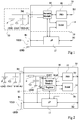
- a typical example of a cryptoprocessor will now be described in connection with the figure 1 .
- a cryptoprocessor equipping a card reader, for example bank cards.
- the present invention can be applied to any type of cryptoprocessor.
- the cryptoprocessor 10 corresponds to an integrated circuit comprising a power supply terminal B1 to which is applied a main supply voltage VDD supplied, for example, from the mains supply.
- the main supply voltage VDD is of the order of 2 volts.
- the cryptoprocessor 10 comprises a microprocessor 12 ( ⁇ P) which performs, in normal operation, the conventional operations specific to the cryptoprocessor 10.
- the cryptoprocessor 10 comprises one or more access terminals (a single terminal B2 being represented in FIG. figure 1 ) through which the microprocessor 12 exchanges data with other components of the reader.
- the cryptoprocessor 10 further comprises a random access memory 14 (RAM) in which the microprocessor 12 is adapted to read and write data, in particular so-called sensitive data.
- the size of the memory 14 depends on the amount of data processed by the cryptoprocessor 10 and is, in a conventional manner, of the order of a few kilobytes, for example 8 kilobytes.
- the cryptoprocessor 10 further comprises a security module 16 (Security Module) or PLC.
- the security module 16 is a logic circuit which has a simpler structure than the structure of the microprocessor 12 and which may comprise a few thousand to a few tens of thousands of logic gates.
- the security module 16 can exchange data with the microprocessor 12 and at least perform write operations in the memory 14.
- the security module 16 can, in addition, exchange data with other components of the reader by the intermediate access terminals (only one terminal B3 is represented in figure 1 ).
- An input / output interface module 18 (PIO) is generally provided between the security module 16 and the access terminal B3.
- the security module 16 can receive signals from the access terminal B3 transmitted by security devices fitted to the reader.
- An example of a security device corresponds to a trellis-type circuit comprising a conductive track whose interruption, representative of an attempt to gain unauthorized access to the reader, results in the provision of an alarm signal to the cryptoprocessor 10.
- another example of a safety device corresponds to a dummy keyboard key permanently ensuring an electrical contact between two conducting tracks in normal operation, a interruption of the contact being representative of an unauthorized access attempt and causing the provision of an alarm signal to the cryptoprocessor 10.
- Another safety device corresponds to a temperature sensor, an excessive temperature being representative of a malfunction. or an unauthorized access attempt and causing the provision of an alarm signal to the cryptoprocessor 10.
- the security module 16 may decide that an attempt to gain unauthorized access takes place upon receipt of a signal alarm at the terminal B3, the detection of a variation of the main supply voltage VDD, the detection of a malfunction of the microprocessor 12, etc.
- the security module 16 detects an unauthorized access attempt, it controls the deletion of the data stored in the memory 14.
- the cryptoprocessor 10 comprises a module, not shown, for supplying a clock signal which elements of the cryptoprocessor 10, in particular the security module 16.
- the security module 16 is powered by the main supply voltage VDD.
- the security module 16 is powered by a backup power source supplying a backup power supply VDD_BU to a terminal B4 of the cryptoprocessor 10.
- the emergency power source comprises a battery P whose one terminal is connected to the terminal B4 and the other terminal is connected to a source of a reference potential, for example the GND mass of the reader.
- a capacitor C1 is connected in parallel across the terminals of the battery P. Below the dashed line 20, the elements of the cryptoprocessor 10 which do not operate when the main supply voltage VDD is not connected.
- the elements of the cryptoprocessor 10 which, when the main supply voltage VDD is not present, continue to operate by being powered by the backup power supply voltage VDD_BU, optionally in one operating mode different from the normal operating mode.
- the module for providing the clock signal operates continuously.
- the security module 16 powered by the battery P, continues to operate and can therefore erase the data stored in the memory 14 when an unauthorized access attempt is made. detected.
- the security module 16 remains energized for a certain time by the capacitor C1.
- the decrease of the voltage across the capacitor C1 is detected by the security module 16 which reacts, as for the detection of an unauthorized access attempt, by the erasure of the sensitive data stored in the memory 14.
- the capacity of the capacitor C1 which generally corresponds to a discrete component, is sufficient to enable the operation of erasing the memory 14 by the security module 16.
- the reader generally comprises a housing formed of an upper housing portion (at which the display screen and the reader keyboard are located) and a lower housing portion.
- the housing contains a motherboard, the electronic components of the reader being connected to one or other of the faces of the motherboard.
- the cryptoprocessor 10 and the capacitor C1 are generally connected on the face of the motherboard facing the upper portion of the housing or upper face.
- the battery P is generally connected to the face of the motherboard facing the lower portion of the housing or lower face. Even if security devices can be provided on both sides of the motherboard, it is generally considered that the level of security of the components connected to the underside of the motherboard is lower than that of the components connected to the upper face of the motherboard. the motherboard to the extent that an intrusion performed on the side of the portion upper housing is usually visible during usual handling of the housing.
- the capacitor C1 is generally disposed on the upper face of the motherboard which has a higher security level than the lower face, it is a discrete component distinct from the cryptoprocessor 10. There is therefore always a risk that a user can access capacitor C1 without an unauthorized access attempt being detected. A disconnection of the capacitor C1, and the battery P, then causes the quasi-instantaneous fall of the backup power supply voltage VDD_BU and therefore, when the main supply voltage VDD is not present, a stop of the operation of the security module 16 without an erase operation of the sensitive data stored in the memory 14 could be performed.
- the dashed line 22 delimits the elements of the reader 10, more precisely the battery P, the capacitor C1 and the electrical connection between the battery P, the capacitor C1 and the access terminal B4, which require special protection to ensure the good operation of the cryptoprocessor 10.
- the figure 2 represents an exemplary embodiment of a cryptoprocessor 30 according to the invention that makes it possible to prevent access to sensitive data during variations of the backup power supply voltage VDD_BU.
- the common elements with the cryptoprocessor 10 of the figure 1 are designated by the same references.
- the cryptoprocessor 30 comprises all the elements of the cryptoprocessor 10 and comprises, in addition, an additional capacitor C2, one terminal of which is connected to a source of a reference potential, for example the GND mass of the reader, and the other of which terminal is connected firstly to a terminal A1 of the security module 16 and secondly to the terminal B4 via a device R (for example a resistor, a diode or other) prohibiting a rapid discharge of the capacitor C2 by an external action on terminal B4.
- a device R for example a resistor, a diode or other
- the terminal B4 is also directly connected to a reset terminal of the security module 16.
- DIFF is the voltage between the terminals A1 and RAZ and V A1 the voltage across the capacitor C2.
- the security module 16 comprises an additional random access memory 32 (Register) of reduced capacity with respect to the random access memory 14 and for which the writing and reading operations can be performed by the processing module 16 over a small number of cycles. clock and low energy cost. This is for example a register of a few hundred bits, for example 256 bits.
- the sensitive data are stored in the memory 14 in an encrypted form, the encryption method used using at least one key, called the primary key.
- the primary key is stored in the additional memory 32 of the security module 16.
- the microprocessor 12 when it wishes to use sensitive data stored in the memory 14, it also reads the primary key stored in the supplementary memory 32 to decrypt the sensitive data stored in the memory 14.
- the security module 16 When detecting an unauthorized access attempt, the security module 16 first clears the primary key stored in the supplementary memory 32 and then optionally erases the sensitive data stored in the memory 14.
- the microprocessor 12 stops working and the security module 16 continues to operate while being powered by the battery P.
- the capacitor C2 is charged by the emergency power supply voltage VDD_BU applied to terminal B4.
- the voltage V Al is then equal to the emergency supply voltage VDD_BU.
- the voltage DIFF is then substantially zero.
- the emergency supply voltage VDD_BU varies, which corresponds, for example, to a deactivation of the battery P or a deliberate manipulation of the voltage VDD_BU
- the voltage at the terminal RAZ varies while the voltage V Al at terminal A1 is maintained at a substantially constant value by capacitor C2.
- the increase in absolute value of the voltage DIFF is detected by the security module 16 as an unauthorized access attempt, for example when it is greater than a determined threshold for a given number of clock cycles.
- the backup power supply VDD_BU may have decreased, the security module 16 is then powered by the additional capacitor C2 until it is discharged.
- the security module 16 first deletes the primary key stored in the secondary memory 32. Then, if its power supply is sufficient, the security module 16 tries to erase the stored sensitive data. in the memory 14.
- the operation of erasing the data stored in the additional memory 32 can be performed quickly with a low energy cost. In particular, it can be performed while the security module 16 is only powered by the capacitor C2. On the other hand, depending on the size of the RAM 14, the capacitance of the capacitor C2 may not be large enough to ensure a sufficient power supply for the module security 16 allowing the erasure of all the sensitive data stored in the memory 14.
- the capacity of the capacitor C2 may be less than a few picofarads. Such a capacity is sufficient to ensure a supply current of the security module 16 of the order of a few hundred nanoamperes during a few clock cycles. This is sufficient to ensure the operation of the security module 16 during the few clock cycles necessary for the detection of an intrusion attempt and the erasure of the additional memory 32. In particular, when the additional memory 32 corresponds to a register, erasing the data stored in the memory 32 can be realized in a single clock cycle.
- the capacitor C2 may be integrated with the other elements of the security module 16.
- the capacitor C2 may correspond to the parasitic capacitances of the MOS transistors constituting the security module 16.
- the capacitor C2 assuring the supply of the security module 16, the protection constraints of the battery P, the capacitor C1 and the electrical connection between the battery P, the capacitor C1 and the access terminal B4 may be less severe than for the circuit shown. in figure 1 .
Landscapes
- Engineering & Computer Science (AREA)
- Physics & Mathematics (AREA)
- Computer Hardware Design (AREA)
- Theoretical Computer Science (AREA)
- Mathematical Physics (AREA)
- Computer Security & Cryptography (AREA)
- Software Systems (AREA)
- General Engineering & Computer Science (AREA)
- General Physics & Mathematics (AREA)
- Storage Device Security (AREA)
Priority Applications (1)
| Application Number | Priority Date | Filing Date | Title |
|---|---|---|---|
| PL08805806T PL2162846T3 (pl) | 2007-05-21 | 2008-05-19 | Kryptoprocesor z udoskonaloną ochroną danych |
Applications Claiming Priority (2)
| Application Number | Priority Date | Filing Date | Title |
|---|---|---|---|
| FR0755148A FR2916560B1 (fr) | 2007-05-21 | 2007-05-21 | Cryptoprocesseur a protection de donnees amelioree |
| PCT/FR2008/050860 WO2008142356A2 (fr) | 2007-05-21 | 2008-05-19 | Cryptoprocesseur a protection de donnees amelioree |
Publications (2)
| Publication Number | Publication Date |
|---|---|
| EP2162846A2 EP2162846A2 (fr) | 2010-03-17 |
| EP2162846B1 true EP2162846B1 (fr) | 2018-04-18 |
Family
ID=38769930
Family Applications (1)
| Application Number | Title | Priority Date | Filing Date |
|---|---|---|---|
| EP08805806.0A Active EP2162846B1 (fr) | 2007-05-21 | 2008-05-19 | Cryptoprocesseur a protection de donnees amelioree |
Country Status (7)
| Country | Link |
|---|---|
| US (1) | US8316242B2 (pl) |
| EP (1) | EP2162846B1 (pl) |
| CA (1) | CA2687582C (pl) |
| ES (1) | ES2675072T3 (pl) |
| FR (1) | FR2916560B1 (pl) |
| PL (1) | PL2162846T3 (pl) |
| WO (1) | WO2008142356A2 (pl) |
Families Citing this family (12)
| Publication number | Priority date | Publication date | Assignee | Title |
|---|---|---|---|---|
| KR100911379B1 (ko) * | 2007-06-14 | 2009-08-10 | 삼성전자주식회사 | 반도체 집적 회로의 해킹 검출기 및 그것의 검출 방법 |
| US8201267B2 (en) * | 2008-10-24 | 2012-06-12 | Pitney Bowes Inc. | Cryptographic device having active clearing of memory regardless of state of external power |
| US9250671B2 (en) | 2011-02-16 | 2016-02-02 | Honeywell International Inc. | Cryptographic logic circuit with resistance to differential power analysis |
| US8378710B1 (en) * | 2011-09-20 | 2013-02-19 | Nxp B.V. | Secure device anti-tampering circuit |
| CN103177753B (zh) * | 2013-04-15 | 2016-07-06 | 东莞市美之尊电子科技有限公司 | 一种带有蓝牙防泄密和防丢的移动存储器及应用方法 |
| CN104681076A (zh) * | 2013-11-28 | 2015-06-03 | 中国航天科工集团第三研究院第八三五七研究所 | 带快速数据自销毁功能的固态硬盘 |
| US11074235B2 (en) * | 2017-08-10 | 2021-07-27 | Io-Tahoe Llc | Inclusion dependency determination in a large database for establishing primary key-foreign key relationships |
| US10489614B2 (en) * | 2017-09-26 | 2019-11-26 | Hewlett Packard Enterprise Development Lp | Tamper detecting cases |
| FR3077673B1 (fr) * | 2018-02-07 | 2020-10-16 | Ingenico Group | Circuit securise d'alimentation de memoire volatile |
| JP7010864B2 (ja) * | 2019-02-26 | 2022-02-10 | ファナック株式会社 | ケースが回路基板から取り外されたか否かを記録するケース開封記録装置及びケース開封記録システム |
| US11221666B2 (en) * | 2019-12-19 | 2022-01-11 | Bae Systems Information And Electronic Systems Integration Inc. | Externally powered cold key load |
| US12260895B2 (en) * | 2021-09-01 | 2025-03-25 | Micron Technology, Inc. | Apparatus with power-based data protection mechanism and methods for operating the same |
Family Cites Families (7)
| Publication number | Priority date | Publication date | Assignee | Title |
|---|---|---|---|---|
| GB2195478B (en) * | 1986-09-24 | 1990-06-13 | Ncr Co | Security device for sensitive data |
| US5027397A (en) * | 1989-09-12 | 1991-06-25 | International Business Machines Corporation | Data protection by detection of intrusion into electronic assemblies |
| US5457748A (en) * | 1992-11-30 | 1995-10-10 | Motorola, Inc. | Method and apparatus for improved security within encrypted communication devices |
| US6292898B1 (en) * | 1998-02-04 | 2001-09-18 | Spyrus, Inc. | Active erasure of electronically stored data upon tamper detection |
| JP2002109900A (ja) * | 2000-09-28 | 2002-04-12 | Mitsubishi Electric Corp | 半導体装置、および半導体記憶装置のテスト方法 |
| WO2002041317A1 (en) * | 2000-11-17 | 2002-05-23 | Fujitsu Limited | Method of creating security medium, device for creating security medium, and reproducing device |
| US7218567B1 (en) * | 2005-09-23 | 2007-05-15 | Xilinx, Inc. | Method and apparatus for the protection of sensitive data within an integrated circuit |
-
2007
- 2007-05-21 FR FR0755148A patent/FR2916560B1/fr active Active
-
2008
- 2008-05-19 CA CA2687582A patent/CA2687582C/en active Active
- 2008-05-19 EP EP08805806.0A patent/EP2162846B1/fr active Active
- 2008-05-19 WO PCT/FR2008/050860 patent/WO2008142356A2/fr not_active Ceased
- 2008-05-19 PL PL08805806T patent/PL2162846T3/pl unknown
- 2008-05-19 ES ES08805806.0T patent/ES2675072T3/es active Active
- 2008-05-19 US US12/600,747 patent/US8316242B2/en active Active
Non-Patent Citations (1)
| Title |
|---|
| None * |
Also Published As
| Publication number | Publication date |
|---|---|
| FR2916560A1 (fr) | 2008-11-28 |
| US20100169671A1 (en) | 2010-07-01 |
| WO2008142356A2 (fr) | 2008-11-27 |
| WO2008142356A3 (fr) | 2009-04-09 |
| EP2162846A2 (fr) | 2010-03-17 |
| CA2687582A1 (en) | 2008-11-27 |
| CA2687582C (en) | 2018-09-11 |
| FR2916560B1 (fr) | 2009-08-07 |
| PL2162846T3 (pl) | 2018-09-28 |
| US8316242B2 (en) | 2012-11-20 |
| ES2675072T3 (es) | 2018-07-06 |
Similar Documents
| Publication | Publication Date | Title |
|---|---|---|
| EP2162846B1 (fr) | Cryptoprocesseur a protection de donnees amelioree | |
| EP1062633B1 (fr) | Dispositifs pour masquer les operations effectuees dans une carte a microprocesseur | |
| US8627116B2 (en) | Power conservation in an intrusion detection system | |
| US8331189B1 (en) | Tamper-protected DRAM memory module | |
| EP2280364A1 (fr) | Détecteur d'injection de fautes dans un circuit intégré | |
| FR2880445A1 (fr) | Unite de commande de fonctionnement en cas de coupure d'alimentation, appareil de stockage en memoire incluant une telle unite et procede pour les faire fonctionner | |
| CA2257339C (fr) | Memoire remanente effacable et programmable electriquement, protegee contre les coupures d'alimentation | |
| KR101108516B1 (ko) | 비휘발성 저장 장치와 방법 | |
| FR2891943A1 (fr) | Procede et circuit de detection de tension transitoire | |
| JP2001256119A (ja) | 自己破壊型半導体装置 | |
| EP1053531B1 (fr) | Dispositif a circuit integre securise par attenuation de signatures electriques | |
| EP1227329A1 (fr) | Circuit de détection de mauvaise connexion d'alimentation | |
| EP2333703B1 (fr) | Composant électronique apte à détecter des attaques actives | |
| US20060028340A1 (en) | Method and apparatus for disabling an integrated circuit (IC) when an attempt is made to bypass security on the IC | |
| EP1272973B1 (en) | Output stage for a communication contact for a data carrier | |
| EP1168621A1 (fr) | Circuit intégré avec dispositif de protection | |
| EP1818846B1 (fr) | Vérification d'intégrité de programmes ou de séquencement d'une machine d'états | |
| FR2810438A1 (fr) | Circuit de detection d'usure | |
| EP1089218B1 (fr) | Circuit d'entrée pour carte à puce à mémoire | |
| FR2834366A1 (fr) | Carte a puce autoverrouillable, dispositif de securisation d'une telle carte et procedes associes | |
| EP1715436A2 (fr) | Protection du déroulement d'un programme exécuté par un circuit intégré ou de données contenues dans ce circuit | |
| JP2006172384A (ja) | 半導体装置 | |
| WO2004029873A1 (fr) | Entite electronique securisee avec gestion du temps | |
| EP2073176A1 (fr) | Système électronique portable avec contrôle d'une consommation d'énergie d'un élément du système | |
| US20230099825A1 (en) | Power supply device, method and secure system |
Legal Events
| Date | Code | Title | Description |
|---|---|---|---|
| PUAI | Public reference made under article 153(3) epc to a published international application that has entered the european phase |
Free format text: ORIGINAL CODE: 0009012 |
|
| 17P | Request for examination filed |
Effective date: 20091218 |
|
| AK | Designated contracting states |
Kind code of ref document: A2 Designated state(s): AT BE BG CH CY CZ DE DK EE ES FI FR GB GR HR HU IE IS IT LI LT LU LV MC MT NL NO PL PT RO SE SI SK TR |
|
| AX | Request for extension of the european patent |
Extension state: AL BA MK RS |
|
| 17Q | First examination report despatched |
Effective date: 20100712 |
|
| DAX | Request for extension of the european patent (deleted) | ||
| RAP1 | Party data changed (applicant data changed or rights of an application transferred) |
Owner name: INGENICO GROUP |
|
| REG | Reference to a national code |
Ref country code: DE Ref legal event code: R079 Ref document number: 602008054915 Country of ref document: DE Free format text: PREVIOUS MAIN CLASS: G06F0021020000 Ipc: G06F0021750000 |
|
| GRAP | Despatch of communication of intention to grant a patent |
Free format text: ORIGINAL CODE: EPIDOSNIGR1 |
|
| RIC1 | Information provided on ipc code assigned before grant |
Ipc: G06F 21/75 20130101AFI20171011BHEP |
|
| INTG | Intention to grant announced |
Effective date: 20171027 |
|
| GRAJ | Information related to disapproval of communication of intention to grant by the applicant or resumption of examination proceedings by the epo deleted |
Free format text: ORIGINAL CODE: EPIDOSDIGR1 |
|
| GRAR | Information related to intention to grant a patent recorded |
Free format text: ORIGINAL CODE: EPIDOSNIGR71 |
|
| GRAS | Grant fee paid |
Free format text: ORIGINAL CODE: EPIDOSNIGR3 |
|
| GRAA | (expected) grant |
Free format text: ORIGINAL CODE: 0009210 |
|
| INTC | Intention to grant announced (deleted) | ||
| AK | Designated contracting states |
Kind code of ref document: B1 Designated state(s): AT BE BG CH CY CZ DE DK EE ES FI FR GB GR HR HU IE IS IT LI LT LU LV MC MT NL NO PL PT RO SE SI SK TR |
|
| INTG | Intention to grant announced |
Effective date: 20180312 |
|
| REG | Reference to a national code |
Ref country code: GB Ref legal event code: FG4D Free format text: NOT ENGLISH |
|
| REG | Reference to a national code |
Ref country code: CH Ref legal event code: EP |
|
| REG | Reference to a national code |
Ref country code: AT Ref legal event code: REF Ref document number: 991220 Country of ref document: AT Kind code of ref document: T Effective date: 20180515 |
|
| REG | Reference to a national code |
Ref country code: IE Ref legal event code: FG4D Free format text: LANGUAGE OF EP DOCUMENT: FRENCH |
|
| REG | Reference to a national code |
Ref country code: DE Ref legal event code: R096 Ref document number: 602008054915 Country of ref document: DE |
|
| REG | Reference to a national code |
Ref country code: ES Ref legal event code: FG2A Ref document number: 2675072 Country of ref document: ES Kind code of ref document: T3 Effective date: 20180706 |
|
| REG | Reference to a national code |
Ref country code: NL Ref legal event code: MP Effective date: 20180418 |
|
| REG | Reference to a national code |
Ref country code: LT Ref legal event code: MG4D |
|
| PG25 | Lapsed in a contracting state [announced via postgrant information from national office to epo] |
Ref country code: NL Free format text: LAPSE BECAUSE OF FAILURE TO SUBMIT A TRANSLATION OF THE DESCRIPTION OR TO PAY THE FEE WITHIN THE PRESCRIBED TIME-LIMIT Effective date: 20180418 |
|
| PG25 | Lapsed in a contracting state [announced via postgrant information from national office to epo] |
Ref country code: BG Free format text: LAPSE BECAUSE OF FAILURE TO SUBMIT A TRANSLATION OF THE DESCRIPTION OR TO PAY THE FEE WITHIN THE PRESCRIBED TIME-LIMIT Effective date: 20180718 Ref country code: LT Free format text: LAPSE BECAUSE OF FAILURE TO SUBMIT A TRANSLATION OF THE DESCRIPTION OR TO PAY THE FEE WITHIN THE PRESCRIBED TIME-LIMIT Effective date: 20180418 Ref country code: FI Free format text: LAPSE BECAUSE OF FAILURE TO SUBMIT A TRANSLATION OF THE DESCRIPTION OR TO PAY THE FEE WITHIN THE PRESCRIBED TIME-LIMIT Effective date: 20180418 Ref country code: NO Free format text: LAPSE BECAUSE OF FAILURE TO SUBMIT A TRANSLATION OF THE DESCRIPTION OR TO PAY THE FEE WITHIN THE PRESCRIBED TIME-LIMIT Effective date: 20180718 Ref country code: SE Free format text: LAPSE BECAUSE OF FAILURE TO SUBMIT A TRANSLATION OF THE DESCRIPTION OR TO PAY THE FEE WITHIN THE PRESCRIBED TIME-LIMIT Effective date: 20180418 |
|
| PG25 | Lapsed in a contracting state [announced via postgrant information from national office to epo] |
Ref country code: HR Free format text: LAPSE BECAUSE OF FAILURE TO SUBMIT A TRANSLATION OF THE DESCRIPTION OR TO PAY THE FEE WITHIN THE PRESCRIBED TIME-LIMIT Effective date: 20180418 Ref country code: LV Free format text: LAPSE BECAUSE OF FAILURE TO SUBMIT A TRANSLATION OF THE DESCRIPTION OR TO PAY THE FEE WITHIN THE PRESCRIBED TIME-LIMIT Effective date: 20180418 |
|
| REG | Reference to a national code |
Ref country code: CH Ref legal event code: PL |
|
| REG | Reference to a national code |
Ref country code: AT Ref legal event code: MK05 Ref document number: 991220 Country of ref document: AT Kind code of ref document: T Effective date: 20180418 |
|
| PG25 | Lapsed in a contracting state [announced via postgrant information from national office to epo] |
Ref country code: PT Free format text: LAPSE BECAUSE OF FAILURE TO SUBMIT A TRANSLATION OF THE DESCRIPTION OR TO PAY THE FEE WITHIN THE PRESCRIBED TIME-LIMIT Effective date: 20180820 |
|
| REG | Reference to a national code |
Ref country code: DE Ref legal event code: R097 Ref document number: 602008054915 Country of ref document: DE |
|
| REG | Reference to a national code |
Ref country code: GR Ref legal event code: EP Ref document number: 20180401624 Country of ref document: GR Effective date: 20190109 |
|
| REG | Reference to a national code |
Ref country code: BE Ref legal event code: MM Effective date: 20180531 |
|
| PG25 | Lapsed in a contracting state [announced via postgrant information from national office to epo] |
Ref country code: SK Free format text: LAPSE BECAUSE OF FAILURE TO SUBMIT A TRANSLATION OF THE DESCRIPTION OR TO PAY THE FEE WITHIN THE PRESCRIBED TIME-LIMIT Effective date: 20180418 Ref country code: RO Free format text: LAPSE BECAUSE OF FAILURE TO SUBMIT A TRANSLATION OF THE DESCRIPTION OR TO PAY THE FEE WITHIN THE PRESCRIBED TIME-LIMIT Effective date: 20180418 Ref country code: MC Free format text: LAPSE BECAUSE OF FAILURE TO SUBMIT A TRANSLATION OF THE DESCRIPTION OR TO PAY THE FEE WITHIN THE PRESCRIBED TIME-LIMIT Effective date: 20180418 Ref country code: CZ Free format text: LAPSE BECAUSE OF FAILURE TO SUBMIT A TRANSLATION OF THE DESCRIPTION OR TO PAY THE FEE WITHIN THE PRESCRIBED TIME-LIMIT Effective date: 20180418 Ref country code: AT Free format text: LAPSE BECAUSE OF FAILURE TO SUBMIT A TRANSLATION OF THE DESCRIPTION OR TO PAY THE FEE WITHIN THE PRESCRIBED TIME-LIMIT Effective date: 20180418 Ref country code: DK Free format text: LAPSE BECAUSE OF FAILURE TO SUBMIT A TRANSLATION OF THE DESCRIPTION OR TO PAY THE FEE WITHIN THE PRESCRIBED TIME-LIMIT Effective date: 20180418 Ref country code: EE Free format text: LAPSE BECAUSE OF FAILURE TO SUBMIT A TRANSLATION OF THE DESCRIPTION OR TO PAY THE FEE WITHIN THE PRESCRIBED TIME-LIMIT Effective date: 20180418 |
|
| REG | Reference to a national code |
Ref country code: IE Ref legal event code: MM4A |
|
| PLBE | No opposition filed within time limit |
Free format text: ORIGINAL CODE: 0009261 |
|
| STAA | Information on the status of an ep patent application or granted ep patent |
Free format text: STATUS: NO OPPOSITION FILED WITHIN TIME LIMIT |
|
| PG25 | Lapsed in a contracting state [announced via postgrant information from national office to epo] |
Ref country code: LI Free format text: LAPSE BECAUSE OF NON-PAYMENT OF DUE FEES Effective date: 20180531 Ref country code: CH Free format text: LAPSE BECAUSE OF NON-PAYMENT OF DUE FEES Effective date: 20180531 |
|
| 26N | No opposition filed |
Effective date: 20190121 |
|
| PG25 | Lapsed in a contracting state [announced via postgrant information from national office to epo] |
Ref country code: LU Free format text: LAPSE BECAUSE OF NON-PAYMENT OF DUE FEES Effective date: 20180519 |
|
| PG25 | Lapsed in a contracting state [announced via postgrant information from national office to epo] |
Ref country code: IE Free format text: LAPSE BECAUSE OF NON-PAYMENT OF DUE FEES Effective date: 20180519 Ref country code: FR Free format text: LAPSE BECAUSE OF NON-PAYMENT OF DUE FEES Effective date: 20180618 |
|
| PG25 | Lapsed in a contracting state [announced via postgrant information from national office to epo] |
Ref country code: BE Free format text: LAPSE BECAUSE OF NON-PAYMENT OF DUE FEES Effective date: 20180531 Ref country code: SI Free format text: LAPSE BECAUSE OF FAILURE TO SUBMIT A TRANSLATION OF THE DESCRIPTION OR TO PAY THE FEE WITHIN THE PRESCRIBED TIME-LIMIT Effective date: 20180418 |
|
| PG25 | Lapsed in a contracting state [announced via postgrant information from national office to epo] |
Ref country code: FR Free format text: LAPSE BECAUSE OF NON-PAYMENT OF DUE FEES Effective date: 20180618 |
|
| PGRI | Patent reinstated in contracting state [announced from national office to epo] |
Ref country code: FR Effective date: 20190520 |
|
| PG25 | Lapsed in a contracting state [announced via postgrant information from national office to epo] |
Ref country code: MT Free format text: LAPSE BECAUSE OF FAILURE TO SUBMIT A TRANSLATION OF THE DESCRIPTION OR TO PAY THE FEE WITHIN THE PRESCRIBED TIME-LIMIT Effective date: 20180418 |
|
| PG25 | Lapsed in a contracting state [announced via postgrant information from national office to epo] |
Ref country code: TR Free format text: LAPSE BECAUSE OF FAILURE TO SUBMIT A TRANSLATION OF THE DESCRIPTION OR TO PAY THE FEE WITHIN THE PRESCRIBED TIME-LIMIT Effective date: 20180418 |
|
| PG25 | Lapsed in a contracting state [announced via postgrant information from national office to epo] |
Ref country code: HU Free format text: LAPSE BECAUSE OF FAILURE TO SUBMIT A TRANSLATION OF THE DESCRIPTION OR TO PAY THE FEE WITHIN THE PRESCRIBED TIME-LIMIT; INVALID AB INITIO Effective date: 20080519 |
|
| PG25 | Lapsed in a contracting state [announced via postgrant information from national office to epo] |
Ref country code: CY Free format text: LAPSE BECAUSE OF FAILURE TO SUBMIT A TRANSLATION OF THE DESCRIPTION OR TO PAY THE FEE WITHIN THE PRESCRIBED TIME-LIMIT Effective date: 20180418 |
|
| PG25 | Lapsed in a contracting state [announced via postgrant information from national office to epo] |
Ref country code: IS Free format text: LAPSE BECAUSE OF FAILURE TO SUBMIT A TRANSLATION OF THE DESCRIPTION OR TO PAY THE FEE WITHIN THE PRESCRIBED TIME-LIMIT Effective date: 20180818 |
|
| REG | Reference to a national code |
Ref country code: GB Ref legal event code: 732E Free format text: REGISTERED BETWEEN 20220331 AND 20220406 |
|
| REG | Reference to a national code |
Ref country code: DE Ref legal event code: R081 Ref document number: 602008054915 Country of ref document: DE Owner name: BANKS AND ACQUIRES INTERNATIONAL HOLDING, FR Free format text: FORMER OWNER: INGENICO GROUP, PARIS, FR Ref country code: DE Ref legal event code: R081 Ref document number: 602008054915 Country of ref document: DE Owner name: BANKS AND ACQUIRERS INTERNATIONAL HOLDING, FR Free format text: FORMER OWNER: INGENICO GROUP, PARIS, FR |
|
| REG | Reference to a national code |
Ref country code: DE Ref legal event code: R081 Ref document number: 602008054915 Country of ref document: DE Owner name: BANKS AND ACQUIRERS INTERNATIONAL HOLDING, FR Free format text: FORMER OWNER: BANKS AND ACQUIRES INTERNATIONAL HOLDING, SURESNES, FR |
|
| PGFP | Annual fee paid to national office [announced via postgrant information from national office to epo] |
Ref country code: DE Payment date: 20250521 Year of fee payment: 18 Ref country code: PL Payment date: 20250422 Year of fee payment: 18 |
|
| PGFP | Annual fee paid to national office [announced via postgrant information from national office to epo] |
Ref country code: GB Payment date: 20250521 Year of fee payment: 18 Ref country code: ES Payment date: 20250627 Year of fee payment: 18 |
|
| PGFP | Annual fee paid to national office [announced via postgrant information from national office to epo] |
Ref country code: IT Payment date: 20250527 Year of fee payment: 18 |
|
| PGFP | Annual fee paid to national office [announced via postgrant information from national office to epo] |
Ref country code: FR Payment date: 20250530 Year of fee payment: 18 |
|
| PGFP | Annual fee paid to national office [announced via postgrant information from national office to epo] |
Ref country code: GR Payment date: 20250523 Year of fee payment: 18 |
|
| REG | Reference to a national code |
Ref country code: ES Ref legal event code: PC2A Owner name: BANKS AND ACQUIRERS INTERNATIONAL HOLDING Effective date: 20250926 |
|
| P01 | Opt-out of the competence of the unified patent court (upc) registered |
Free format text: CASE NUMBER: UPC_APP_0000319_2162846/2026 Effective date: 20260106 |