EP2159706A1 - Operation processing apparatus and operation processing method - Google Patents
Operation processing apparatus and operation processing method Download PDFInfo
- Publication number
- EP2159706A1 EP2159706A1 EP07767196A EP07767196A EP2159706A1 EP 2159706 A1 EP2159706 A1 EP 2159706A1 EP 07767196 A EP07767196 A EP 07767196A EP 07767196 A EP07767196 A EP 07767196A EP 2159706 A1 EP2159706 A1 EP 2159706A1
- Authority
- EP
- European Patent Office
- Prior art keywords
- tsb
- address
- translation pair
- address translation
- arithmetic processing
- Prior art date
- Legal status (The legal status is an assumption and is not a legal conclusion. Google has not performed a legal analysis and makes no representation as to the accuracy of the status listed.)
- Granted
Links
- 238000003672 processing method Methods 0.000 title claims description 18
- 230000015654 memory Effects 0.000 claims abstract description 145
- 238000000034 method Methods 0.000 claims description 79
- 238000012795 verification Methods 0.000 claims description 9
- 238000010586 diagram Methods 0.000 description 12
- 238000005516 engineering process Methods 0.000 description 10
- 239000000872 buffer Substances 0.000 description 5
- 230000000694 effects Effects 0.000 description 5
- 238000004364 calculation method Methods 0.000 description 4
- 230000006870 function Effects 0.000 description 3
- 238000009434 installation Methods 0.000 description 3
- 239000012536 storage buffer Substances 0.000 description 2
- 238000004590 computer program Methods 0.000 description 1
- 230000010354 integration Effects 0.000 description 1
Images


Classifications
-
- G—PHYSICS
- G06—COMPUTING; CALCULATING OR COUNTING
- G06F—ELECTRIC DIGITAL DATA PROCESSING
- G06F12/00—Accessing, addressing or allocating within memory systems or architectures
- G06F12/02—Addressing or allocation; Relocation
- G06F12/08—Addressing or allocation; Relocation in hierarchically structured memory systems, e.g. virtual memory systems
- G06F12/10—Address translation
- G06F12/1027—Address translation using associative or pseudo-associative address translation means, e.g. translation look-aside buffer [TLB]
-
- G—PHYSICS
- G06—COMPUTING; CALCULATING OR COUNTING
- G06F—ELECTRIC DIGITAL DATA PROCESSING
- G06F2212/00—Indexing scheme relating to accessing, addressing or allocation within memory systems or architectures
- G06F2212/68—Details of translation look-aside buffer [TLB]
- G06F2212/681—Multi-level TLB, e.g. microTLB and main TLB
Definitions
- the present invention relates to an arithmetic processing apparatus, an arithmetic processing program, and an arithmetic processing method.
- the "virtual storage method” is a technology that makes a memory capacity greater than an actual memory capacity in a computer appear to be provided on the computer by using an external memory device (e.g., a hard disk device) as a save area of a memory.
- an external memory device e.g., a hard disk device
- the "virtual storage method” temporarily saves less-frequently-used information among information on the memory to a swap area that has been secured within the hard disk device by an OS, to temporarily compensate for the insufficiency in the memory capacity.
- a virtual address VA
- PA physical address
- a virtual address is used.
- a physical address is an address assigned to a component of a memory.
- a computer employing the virtual storage method stores a list (hereinafter referred to as "page table") of address translation pairs (translation table entry: TTE) for translating virtual addresses into physical addresses.
- the page table is stored in a translation storage buffer (TSB) area of a main memory.
- TTB translation storage buffer
- CPU central processing unit
- TTE-tag virtual address
- TTE-data physical address
- TLB translation-lookaside buffer
- the CPU To perform a memory access with such a configuration, the CPU first searches the TLB. For the TLB search, the CPU uses a virtual address and a context ID (a unique ID for each process). If the values used for the TLB search and values stored in the TLB match each other with respect to these two, it is assumed that an address translation result is present in the TLB, and the CPU obtains the address translation result. When the address translation result corresponding to the requested address and context ID is present in the TLB, it is called a TLB hit. When not present, it is called a TLB miss (memory management unit-MISS: MMU-MISS). When a TLB miss occurs, an MMU-MISS-TRAP is generated. The CPU thus reports the generation of MMU-MISS-TRAP to the OS and the OS that has been reported performs a trap handling process with respect to the CPU.
- MMU-MISS memory management unit-MISS
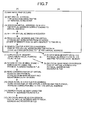
- FIG. 7 is a diagram for explaining the conventional technologies. Inherently, a memory access process performed by the CPU is branched depending on a plurality of determinations during the process. However, for convenience in clearly explaining differences between (A) and (B), in FIG. 7 , the process is illustrated without determinations and a distinguishing a normal trap handling process from other processes. In FIG. 7 , the portion surrounded by a rectangle indicates steps common between (A) and (B).
- (A) in FIG. 7 If, during a memory access, the CPU fails in the TLB search (TLB miss) with a certain virtual address specified by the OS, then an MMU-MISS-TRAP is generated in the CPU (see (1)). The CPU then reports the MMU-MISS-TRAP to the OS, and thus the OS performs a trap handling process for the CPU. Specifically, the CPU sets the certain virtual address, for which the MMU-MISS-TRAP has been generated, in a register (see (2)). Then, based on the virtual address, the CPU generates a TSB virtual address that corresponds to the virtual address (see (3)).
- a TSB virtual address is a virtual address in the TSB area storing an address translation pair corresponding to the virtual address. The CPU sets the generated TSB virtual address in the register (See (4)).
- the CPU reads the virtual address and the TSB virtual address set in the register from the register (see (5)) and searches the TLB for an address translation pair of the TSB virtual address and a TSB physical address (TSB pointer) corresponding to the TSB virtual address (see (6)). The CPU then search a cache memory using the TSB physical address retrieved from the TLB (see (7)).
- an address translation pair (address translation pair of the virtual address and the physical address) is not retrieved as a result of searching the cache memory (i.e., that a cache miss occurs).
- the CPU searches a main memory using the TSB physical address retrieved from the TLB (see (8)), reads the corresponding address translation pair from the main memory, and registers it in the cache memory (See (9)).
- the CPU again searches the TLB for the address translation pair of the TSB virtual address and the TSB physical address corresponding to the TSB virtual address (see (10)).
- the CPU searches the cache memory using the TSB physical address retrieved from the TLB (see (11)). Since the address translation pair is retrieved as a result of searching the cache memory (i.e., since the address translation pair is already registered in the cache memory at (9), cache miss does not occur), the CPU reads the address translation pair from the cache memory and registers it in the TLB (see (12)). In this way, when the CPU searches the TLB again for the certain virtual address, there is going to be a TLB hit.
- Patent Literature 1 a technique is proposed, as illustrated in which, apart from a normal trap handling process, the CPU searches the main memory using the TSB physical address retrieved from the TLB, obtains the address translation pair from the main memory, and pre-fetches the obtained address translation pair in the cache memory, as illustrated at (7) at (B) in FIG. 7 .
- the penalty upon a TLB miss is still big as explained below. That is, in the conventional technology, the CPU still consumes time in the process of obtaining the address translation pair of the virtual address and the physical address from the TSB area of the main memory and pre-fetching that address translation pair in the cache memory. Specifically, in the conventional technology, for the CPU to obtain the address translation pair from the TSB area, the TSB physical address must be searched from the TLB, and this search consumes time. Moreover, the TSB virtual address must be calculated in the conventional technology, and the complexity in the calculation of the TSB virtual address results in an increase in the circuit scale and the installation cost.
- the present invention has been made to solve the above problems in the conventional technologies and it is an object of the present invention to provide an arithmetic processing apparatus, an arithmetic processing program, and an arithmetic processing method that enable reduction in the penalty upon a TLB miss.
- an invention according to claim 1 is an arithmetic processing apparatus that accesses a memory unit including a TSB area storing an address translation pair for translating a virtual address into a physical address.
- the arithmetic processing apparatus includes a TLB that stores a part of the TSB area; a cache memory that temporarily stores the address translation pair; a TSB base-physical-address storing unit that stores a TSB base physical address that is a starting physical address of the address translation pair stored in the memory unit; a TSB pointer calculating unit that calculates, based on the TSB base physical address and a virtual address to be converted, a TSB pointer used in obtaining a corresponding address translation pair from the TSB area; and a translation pair obtaining unit that obtains an address translation pair corresponding to the virtual address to be converted from the TSB area using the TSB pointer calculated and stores the address translation pair in the cache memory, if the address translation pair corresponding to
- an invention according to claim 2 is characterized in that if the address translation pair corresponding to the virtual address to be converted is not retrieved from the TLB, the translation pair obtaining unit verifies, via a trap handling process of an OS, whether the address translation pair is stored in the cache memory, and the translation pair obtaining unit stores the address translation pair of the address translation target obtained from the TSB area using the TSB pointer in the cache memory prior to the verification via the trap handling process.
- an invention according to claim 3 is characterized in that if the virtual address to be converted is not stored in the cache memory, the translation pair obtaining unit registers the address translation pair in the TLB after obtaining the address translation pair from the TSB area and storing the address translation pair in the cache memory.
- the invention according to claim 4 is characterized in that the arithmetic processing apparatus further includes a register unit that controls obtaining of the address translation pair from the TSB area, and based on information stored in the register, the arithmetic processing apparatus controls obtaining of an address translation pair from the TSB area by the translation pair obtaining unit.
- the invention according to claim 5 is characterized in that when a hardware error occurs within the arithmetic processing, the translation pair obtaining unit forbids obtaining of an address translation pair from the TSB area by the translation pair obtaining unit.
- the invention according to claim 6 is an arithmetic processing method by an arithmetic processing apparatus that accesses a memory unit including a TSB area storing an address translation pair for translating a virtual address into a physical address and that includes a TLB storing a part of the TSB area and a cache memory temporarily storing the address translation pair.
- the arithmetic processing method includes the steps of: storing a TSB base physical address that is a starting physical address of an address translation pair stored in the memory unit; calculating, based on the TSB base physical address and a virtual address to be converted, a TSB pointer used in obtaining a corresponding address translation pair from the TSB area; and obtaining an address translation pair corresponding to the virtual address to be converted from the TSB area using the TSB pointer calculated and storing the address translation pair in the cache memory, if the address translation pair corresponding to the virtual address to be converted is not retrieved from the TLB or the cache memory.
- the invention according to claim 7 is characterized in that the arithmetic processing method includes the steps of: if the address translation pair corresponding to the virtual address to be converted is not retrieved from the TLB, verifying, via a trap handling process of an OS, whether the address translation pair is stored in the cache memory; and storing the address translation pair of the address translation target obtained from the TSB area using the TSB pointer in the cache memory prior to the verification via the trap handling process.
- the invention according to claim 8 is characterized in that the arithmetic processing method includes the step of: if the virtual address to be converted is not stored in the cache memory, registering the address translation pair in the TLB after obtaining the address translation pair from the TSB area and storing the address translation pair in the cache memory.
- the invention according to claim 9 is characterized in that the arithmetic processing method further includes a register that controls obtaining of the address translation pair from the TSB area; and the step of, based on information stored in the register, controlling obtaining of an address translation pair from the TSB area.
- the invention according to claim 10 is characterized in that the arithmetic processing method further includes the step of: when a hardware error occurs within the arithmetic processing, forbidding obtaining of an address translation pair from the TSB area.
- an arithmetic processing apparatus accesses a memory unit including a TSB area storing an address translation pair for translating a virtual address into a physical address.
- the arithmetic processing apparatus includes a TLB that stores therein a part of the TSB area, a cache memory that temporarily stores therein the address translation pair, and a TSB base-physical-address storing unit that stores therein a TSB base physical address that is a starting physical address of the address translation pair stored in the memory unit. Based on the TSB base physical address and a virtual address to be converted, a TSB pointer is calculated that is used in obtaining an address translation pair from the TSB area.
- the address translation pair corresponding to the virtual address to be converted is not found in the TLB or the cache memory, the address translation pair corresponding to the virtual address to be converted is obtained from the TSB area using the calculated TSB pointer and stored in the cache memory. As a result, it is possible to reduce the penalty upon a TLB miss.
- a "virtual storage method” is a technology that makes a memory capacity greater than an actual memory capacity in a computer appear to be provided on the computer by using an external memory device as a save area of a memory.
- a "virtual address (VA)” and a “physical address (PA)” are used.
- VA virtual address
- PA physical address
- a “physical address” is an address assigned to a component of a memory.
- a computer employing the "virtual storage method stores a list (hereinafter referred to as "page table") of address translation pairs (translation table entry: TTE) for translating "virtual addresses” into “physical addresses” in a “translation storage buffer (TSB) area” of a main memory.
- TTE translation table entry
- a central processing unit CPU
- CPU central processing unit
- TLB translation-lookaside buffer
- an OS When an application side performs reading and writing (memory access) with respect to the memory, first, an OS specifies a certain "virtual address" to the CPU. The CPU then searches the "TLB” for the certain "virtual address” specified by the OS. If the CPU fails in the search (i.e., when a TLB miss occurs), the CPU verifies, as a trap handling process, whether an address translation pair related to the certain "virtual address" (address translation pair with the "physical address” corresponding to the certain "virtual address”) is stored in a "cache memory". If stored, then the address translation pair is registered in the "TLB".
- the address translation pair is obtained from the "TSB area", stored in the "cache memory” for the time being, and then registered in the "TLB".
- the CPU searches the "TLB” again for the certain "virtual address” for which the TLB miss has occurred, the CPU will not fail in the search (i.e., a TLB hit will occur).
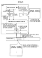
- FIG. 1 is a diagram for explaining the outline and features of the arithmetic processing apparatus according to the first embodiment.
- the arithmetic processing apparatus according to the first embodiment is implemented as a program executed in a control circuit or an instruction control unit provided in a CPU.
- the arithmetic processing apparatus is outlined, with a configuration including a main memory with a TSB area and the CPU including a TLB and a (L2) cache memory, as performing as a trap handling process, upon a TLB search failure (TLB miss), verification of whether an address translation pair is stored in the (L2) cache memory, and if stored, registration of the stored address translation pair in the TLB , and if not stored, obtainment of the address translation pair from the TSB area, storage of it in the cache memory, and then registration of it in the TLB.
- TLB miss TLB search failure
- the main feature is the reduction in the penalty upon a TLB miss.
- the arithmetic processing apparatus stores therein upon a store instruction from an OS a TSB base physical address of the address translation pair related to the virtual address specified in a TLB search (starting physical address of the address translation pair stored in a main memory) (see (1) in FIG. 1 ). Specifically, the arithmetic processing apparatus stores the TSB base physical address in a register (TSB-PreFetch-REGister: TSB-PF-REG; corresponding to a "TSB base-physical-address storing unit" mentioned in the claims).
- TLB-PreFetch-REGister TSB-PF-REG
- the arithmetic processing apparatus Upon a TLB search failure (TLB miss) in such a configuration, the arithmetic processing apparatus substitutes the TSB base physical address stored in the TSB-PF-REG and the virtual address specified in the TLB search in a predetermined formula and calculates a TSB pointer (a pointer used in obtaining the address translation pair related to the certain virtual address from the TSB) (see (2) in FIG. 1 ). Specifically, the arithmetic processing apparatus calculates the TSB pointer at a TSB prefetch control circuit.
- the arithmetic processing apparatus obtains the address translation pair from the TSB area using the calculated TSB pointer and stores the obtained address translation pair in the (L2) cache memory (see (3) in FIG. 1 ).
- the arithmetic processing apparatus upon a TLB search failure (TLB miss), performs the normal trap handling process apart from the above described process, and as illustrated at step (4) in FIG. 1 , "verification of whether the address translation pair is stored in the (L2) cache memory" is performed after step (3).
- the arithmetic processing apparatus is able to reduce the penalty upon a TLB miss.
- the arithmetic processing apparatus upon a TLB miss, pre-fetches the address translation pair concurrently with (or prior to) the normal trap handling process and stores the address translation pair in the (L2) cache memory prior to performing the verification in the trap handling process. That prevents a cache miss from occurring during the trap handling process. As a result, it becomes possible to conceal memory latency and speed up the trap handling process. In other words, since a cache hit occurs without fail when a memory access to the TSB is requested in the trap handling process, it is possible to register the address translation pair instantly in the TLB.
- the arithmetic processing apparatus does not need to search the TLB for the TSB physical address but only needs to use the TSB base physical address and virtual address that have already been stored in the register.
- the amount of time for the process of searching the TLB for the TSB physical address is reduced, thus reducing the penalty upon a TLB miss.
- the calculation of TSB physical address is simple, and thus it is possible to reduce the circuit scale and the installation cost.
- FIG. 2 is a block diagram of the configuration of the arithmetic processing apparatus according to the first embodiment.
- FIG. 3 is a diagram for explaining the TSB-PF-REG (TSB base-physical-address storing unit).
- FIG. 4 is a diagram for explaining a formula for calculating a TSB pointer.
- FIG. 5 is a block diagram of a general configuration of a CPU.
- FIG. 2 a configuration of the arithmetic processing apparatus according to the first embodiment is explained with reference to FIG. 2 .
- the arithmetic processing apparatus according to the first embodiment is implemented as a program executed in a control circuit or an instruction control unit provided in a CPU 10.
- a control circuit or an instruction control unit provided in a CPU 10.
- FIG. 2 does not represent the entire configuration of the arithmetic processing apparatus according to the present embodiment.
- the CPU 10 is closely related to the present embodiment and, as illustrated in FIG. 2 , mainly includes an instruction control unit 11, an execution unit 12, a TLB 13, a TSB-PF-REG 14, a TSB prefetch control circuit 15, and a (L2) cache memory 16.
- a main memory 20 including a TSB area 21 is provided as a memory device outside the CPU 10.
- the TLB 13 stores some of address translation pairs from a page table stored in the TSB area 21. Specifically, the TLB 13 stores therein an address translation pair of a virtual address ("VA” in FIG. 2 ) and a physical address ("PA” in FIG. 2 ). In addition, the TLB 13 includes a MATCH circuit as illustrated in FIG. 2 . Upon receiving an instruction to search the TLB 13 ("TLB search” in FIG. 2 ) from the instruction control unit 11, the MATCH circuit determines whether values used in the search through the TLB 13 and values stored in the TLB 13 match, with respect to the two, the virtual address ("VA” in FIG. 2 ) and the context ID ("ctxt” in FIG. 2 ), and determines it to be a TLB hit ("TLB-HIT" in FIG. 2 ) if matched and a TLB miss ("TLB-MISS" in FIG. 2 ) if not matched.
- TLB search an instruction to search the TLB 13
- the MATCH circuit determines whether values used in
- the TSB-PF-REG 14 stores therein a TSB base physical address of an address translation pair related to a certain virtual address (starting physical address of the address translation pair stored in the main memory 20). Specifically, the TSB-PF-REG 14, upon a store instruction from an OS, stores therein in advance a TSB base physical address of an address translation pair related to a certain virtual address specified in a search ("access VA" in FIG. 2 ). The TSB base physical address is the base (starting physical address) of the physical address in the main memory 20 storing the address translation pair.
- the TSB-PF-REG 14 corresponds to a "TSB base-physical-address storing unit" mentioned in the claims.
- the TSB-PF-REG 14 is arranged, for example, as eight registers per thread.
- a "Context number ⁇ 0" is mainly for a "user mode”.
- two types of TLB (1st/2nd) for "instruction” and for "data” may be specified.
- the TSB-PF-REG 14 may also specify a page size.
- a "TSB base in physical” field specifies a TSB base pointer with a physical address.
- a "Valid” field specifies a selection of performing pre-fetching when a "valid bit” is “1” and not performing pre-fetching when the "valid bit” is "0".
- a "page_size” field specifies the page size of the TSB area 21.
- a "TSB_size” field specifies the number of entries (512x2**TSB_size) in the TSB area 21.
- the execution unit 12 carries out operations. Features closely related to the present embodiment are explained.
- the execution unit 12 stores a TSB physical address in the TSB-PF-REG 14, apart from a normal trap handling process.
- the instruction control unit 11 receives an instruction from the OS and controls the flow of process performed by the CPU 10. The features closely related to the present embodiment are explained.
- the instruction control unit 11 performs, apart from a normal trap handling process, a process of searching the TLB 13 for a certain virtual address specified by the OS, a process of storing a TSB base physical address in the TSB-PF-REG 14, a process of calculating a TSB pointer, and a process of storing an address translation pair obtained from the TSB area 21 in the (L2) cache memory 16.
- the instruction control unit 11 implements, in tandem with the TSB prefetch control circuit 15 described later, functions that correspond to a "TSB pointer calculating unit" and a "translation pair obtaining unit” mentioned in the claims.
- the instruction control unit 11 searches the TLB 13 ("TLB search" in FIG. 2 ) for a certain virtual address ("access VA" in FIG. 2 ) specified by the OS. If the search fails (TLB miss occurs), the instruction control unit 11 sends a TLB miss signal indicating the occurrence of the TLB miss, the virtual address, and a context number to the TSB prefetch control circuit 15, apart from controlling the normal trap handling process.
- the TSB prefetch control circuit 15 Upon receiving the TLB miss signal, the virtual address, and the context number from the instruction control unit 11, the TSB prefetch control circuit 15 selects a TSB-PF-REG 14 to be read out, depending on the value of the context number and whether the signal is from an instruction TLB or a signal from a data TLB. Then, the TSB prefetch control circuit 15 reads the "1st-REG" and the "2nd-REG" from the TSB-PF-REG 14 in two cycles, calculates a TSB pointer (TSB prefetch address) for each, and issues a TSB prefetch request (a request for obtaining an address translation pair from the TSB area 21, depicted as "TSB-PF-REQ" in FIG. 2 ).
- TSB prefetch address a request for obtaining an address translation pair from the TSB area 21, depicted as "TSB-PF-REQ" in FIG. 2 .
- TSB prefetch control circuit 15 issues the TSB prefetch request to both.
- the TSB prefetch control circuit 15 then reads the selected TSB-PF-REG 14 and, if the "valid bit" is "0", refrains from issuing the TSB prefetch request.
- the TSB prefetch control circuit 15 refrains from issuing the TSB prefetch request if an address parity error or a register parity error is detected.
- the TSB prefetch control circuit 15 substitutes the value read from the selected TSB-PF-REG 14 and the virtual address transmitted from the instruction control unit 11 in a predetermined formula and calculates a TSB pointer. Using the TSB pointer calculated, the TSB prefetch control circuit 15 issues a TSB prefetch request, and sends, together with a request signal, the TSB pointer calculated. The TSB prefetch control circuit 15 obtains the address translation pair from the main memory 20 using the TSB pointer and stores the obtained address translation pair in the (L2) cache memory 16.
- the TSB prefetch control circuit 15 calculates the TSB pointer using a predetermined formula like the one illustrated in FIG. 4 .
- “TSB pointer” represents a TSB prefetch address
- “TSB_base” represents the “TSB base in physical” field in the TSB-PF-REG 14
- “N” represents the "TSB_size”
- “page_sz” represents the TSB page size
- " represents bit concat (concatenation of character strings).
- the TSB prefetch control circuit 15 may be implemented using, for example, an existing control circuit such as a control circuit having a prefetch function of a (L1) cache memory.
- FIG. 5 does not represent the entire configuration of the arithmetic processing apparatus according to the present embodiment.
- the arithmetic processing apparatus according to the present embodiment may not include all of the components illustrated in FIG. 5 .
- numbers (1) to (6) given in FIG. 5 are assigned for convenience in explanation and do not represent the sequence of steps.
- a CPU 100 generally includes an instruction control unit 200, an execution unit 250, a TLB 300, an L1 instruction TAG 400, an L1 data TAG 450, an L1 instruction cache 500, an L1 data cache 550, and an L2 cache 600.
- the CPU 100 carries out an operation according to an instruction stored in a memory device installed in a computer and processes information according to the result of the operation.
- instruction does not refer to a command that is input by a user of the computer from, for example, a keyboard or a command as a line of a program programmed by a developer.
- a command is first translated into computer-comprehensible machine language, then reconfigured in computer-recognizable binary numbers, and consequently divided in minimum processible units that the CPU 100 is able to process as the "instruction".
- the instruction control unit 200 controls the flow of processes performed by the CPU 100. Specifically, the instruction control unit 200 reads an "instruction" to be processed in the CPU 100 from a memory device, interprets it, and sends the interpretation result to the execution unit 250 (see (1) in FIG. 5 ).
- the execution unit 250 carries out an operation. Specifically, the execution unit 250 reads "data" that is the target of the "instruction” from a memory device, performs an operation according to the "instruction” interpreted by the instruction control unit 200, and sends the result of operation to the instruction control unit 200 (see (1) in FIG. 5 ).
- the instruction control unit 200 and the execution unit 250 read the "instruction" and "data” from a memory device.
- That memory device may be a cache memory such as a primary (Level 1) cache (hereinafter, “L1 cache”) and a secondary (Level 2) cache (hereinafter, "L2 cache”).
- L1 cache primary (Level 1) cache
- L2 cache secondary cache
- the cache memories are installed inside the CPU 100 in a hierarchical structure.
- the L1 instruction cache 500 that is an L1 cache dedicated to instructions the L1 data cache 550 that is an L1 cache dedicated to data are provided, and the L2 cache 600 is provided as an L2 cache memory.
- a main memory 700 is not part of the CPU 100 but is provided external to the CPU 100 as a memory device.
- the L1 instruction cache 500 and the L1 data cache 550 are able to operate by the same clock as the CPU 100 and to speedily respond to a request from the instruction control unit 200 or the execution unit 250 (see (2) in FIG. 5 ).
- the total capacity of the L1 instruction cache 500 and the L1 data cache 550 is about 32K to 128K and thus is not capable of storing a large volume of information.
- the L2 cache 600 stores less frequently used information (see (3) in FIG. 5 ).
- the information that cannot be stored in the L2 cache 600 is stored in the main memory 700 (see (4) in FIG. 5 ).
- the "instruction” and “data” are in the main memory 700 while nothing is stored in the L1 instruction cache 500, the L1 data cache 550, or the L2 cache 600.
- these "instruction” and “data” are loaded in the L1 instruction cache 500 and L1 data cache 550, or the L2 cache 600.
- the instruction control unit 200 and the execution unit 250 read the "instruction” and “data” from the high-speed L1 instruction cache 500 and L1 data cache 550, or the L2 cache 600, and not from the low-speed main memory 700.
- the "instruction” and “data” the instruction control unit 200 and the execution unit 250 try to read are not necessarily stored in the L1 instruction cache 500 and the L1 data cache 550.
- the instruction control unit 200 and the execution unit 250 use the L1 instruction TAG 400 or the L1 data TAG 450. That is, as the "instruction” and “data” are loaded in the L1 instruction cache 500 and the L1 data cache 550, numeric values indicating at which addresses in the main memory 700 the "instruction” and “data” are stored are set in the L1 instruction TAG 400 and the L1 data TAG 450.
- the instruction control unit 200 and the execution unit 250 make an inquiry to the L1 instruction TAG 400 and the L1 data TAG 450 to verify whether the "instruction" and "data” to be read are stored in the L1 instruction cache 500 and the L1 data cache 550.
- the "virtual storage method” is employed as already described.
- the instruction control unit 200 and the execution unit 250 first specify a "virtual address" to the TLB 300 (see (5) in FIG. 5 ) and, after the TLB 300 translates it into a "physical address", an inquiry is made to the L1 instruction TAG 400 and the L1 data TAG 450 (see (6) in FIG. 5 ).
- the arithmetic processing apparatus includes the TSB-PF-REG 14 and the TSB prefetch control circuit 15 as structural components.
- the instruction control unit 11 controls the calculation of the TSB pointer and the obtaining of the address translation pair, and thus it is possible to reduce the penalty upon a TSB miss.
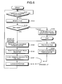
- FIG. 6 is a flowchart indicating the steps of the process by the arithmetic processing apparatus according to the first embodiment. From among the steps of the process illustrated in FIG. 6 , Steps S105 to S110 represent a normal trap handling process. Steps S108 and S109 represent the steps of the process characteristic to the arithmetic processing apparatus according to the first embodiment and to achieve the effects of the present embodiment, these steps are fed back to the normal trap handling process.
- the instruction control unit 11 determines whether a memory access request has been received (Step S101). If a memory access request has not been received (No at Step S101), the instruction control unit 11 returns to the step of determining whether a memory access request has been received.
- Step S101 If a memory access request has been received (Yes at Step S101), the instruction control unit 11 searches the TLB 13 for a certain virtual address specified by the OS (Step S102).
- the instruction control unit 11 determines whether the determination result determined by the MATCH circuit in the TLB 13 is a TLB miss (MMU-MISS) (Step S103). If it is not a TLB miss (No at Step S103), then the instruction control unit 11 performs a search through a cache memory and other processes using an address translation result (Step S104) and ends the processes.
- MMU-MISS TLB miss
- the instruction control unit 11 performs a normal trap handling process. Specifically, the instruction control unit 11 sets the certain virtual address, for which the MMU-MISS-TRAP has been generated, in a register. Then, based on the virtual address, the instruction control unit 11 generates a TSB virtual address that corresponds to the virtual address and sets it in the register. Subsequently, the instruction control unit 11 reads the virtual address and the TSB virtual address, which have been set in the register from the register (Step S105) and performs Step S106 as the normal trap handling process.
- the arithmetic processing apparatus is characterized in that , prior to (or concurrently with) reporting the MMU-MISS-TRAP to the OS, a TSB pointer is calculated from the TSB base physical address that has been stored in advance in the TSB-PF-REG 14 and the MMU-MISSed virtual address, a required address translation pair is pre-fetched, and the address translation pair is stored in the (L2) cache memory. As a result, it becomes possible to speedily provide the address translation pair upon attempting to obtain this address translation pair by the trap handling process.
- the instruction control unit 11 performs TSB pre-fetching apart form the normal trap handling process (Step S108). Specifically, the instruction control unit 11 sends a TLB miss signal indicating the occurrence of the TLB miss, the virtual address, and a context number to the TSB prefetch control circuit 15. Then, the TSB prefetch control circuit 15 reads the TSB-PF-REG 14, and substitutes the read value and the virtual address transmitted from the TLB 13 into a predetermined formula, to calculate a TSB pointer. Subsequently, the TSB prefetch control circuit 15 issues a TSB prefetch request using the calculated TSB pointer and sends a request signal and the calculated TSB pointer (Step S108).
- the TSB prefetch control circuit 15 obtains from the main memory 20 the address translation pair using the TSB pointer and makes the (L2) cache memory 16 hold the obtained address translation pair (Step S109). Because the address translation pair is thus held in the (L2) cache memory 16 at Step S109, in the normal trap handling process, upon start of a memory access to the TSB area 21 (Step S107), a cache hit occurs without fail.
- the arithmetic processing apparatus accesses a memory unit including a TSB area storing an address translation pair for translating a virtual address into a physical address.
- the arithmetic processing apparatus includes a TLB that stores therein a part of the TSB area, a cache memory that temporarily stores therein the address translation pair, and a TSB base-physical-address storing unit that stores therein a TSB base physical address that is a starting physical address of the address translation pair stored in the memory unit. Based on the TSB base physical address and a virtual address to be converted, a TSB pointer is calculated that is used in obtaining an address translation pair from the TSB area.
- the address translation pair corresponding to the virtual address to be converted is not retrieved from the TLB or the cache memory, the address translation pair corresponding to the virtual address to be converted is obtained from the TSB area using the calculated TSB pointer and stored in the cache memory. As a result, it is possible to reduce the penalty upon a TLB miss.
- the arithmetic processing apparatus upon a TLB miss, pre-fetches the address translation pair concurrently with (or prior to) the normal trap handling process and stores the address translation pair in the (L2) cache memory prior to verification in the trap handling process.
- occurrence of a cache miss is prevented during the trap handling process, and it is possible to conceal memory latency and to speed up the trap handling process.
- a cache hit since a cache hit is obtained without fail upon a memory access request to the TSB in the trap handling process, it is possible to register the address translation pair instantly in the TLB.
- the arithmetic processing apparatus does not need to search the TLB for the TSB physical address but only needs to use the TSB base physical address and the virtual address that have already been stored in a register. Therefore, the amount of time required to search the TLB for the TSB physical address is shortened, reducing the penalty upon a TLB miss. Furthermore, since the calculation of the TSB physical address is simple, it is possible to reduce the circuit scale and thus the installation cost.
- each structural element of each apparatus illustrated in the drawings are conceptual and functional, and does not have to be physically configured as illustrated (such as in FIG. 2 ). That is, the specific embodiments of distribution or integration of each apparatus are not limited to those illustrated in the drawings, and all or a part of it may be distributed or integrated functionally or physically in any units based on various types of loads and use conditions. All or a part of the process functions performed by each apparatus may be realized by a CPU or a computer program analyzed and executed by the CPU, or realized as hardware by wired logic.
- the arithmetic processing method described in the present embodiment may be implemented by executing in a CPU a program prepared in advance.
- the program may be distributed over a network such as the Internet.
- the program may be stored in a computer-readable recording medium such as a hard disk, a flexible disk (FD), a CD-ROM, an MO, or a DVD to be read from the recording medium and executed by a CPU.
- the arithmetic processing apparatus, the arithmetic processing program, and the arithmetic processing method according to the present invention is useful for accessing a memory unit including a TSB area storing address translation pairs for translating virtual addresses into physical addresses and particularly suitable for reducing the penalty upon a TLB miss.
Landscapes
- Engineering & Computer Science (AREA)
- Theoretical Computer Science (AREA)
- Physics & Mathematics (AREA)
- General Engineering & Computer Science (AREA)
- General Physics & Mathematics (AREA)
- Memory System Of A Hierarchy Structure (AREA)
Abstract
Description
- The present invention relates to an arithmetic processing apparatus, an arithmetic processing program, and an arithmetic processing method.
- Conventionally, many computers employ the "virtual storage method". The "virtual storage method" is a technology that makes a memory capacity greater than an actual memory capacity in a computer appear to be provided on the computer by using an external memory device (e.g., a hard disk device) as a save area of a memory. Thus, when the memory capacity becomes insufficient, the "virtual storage method" temporarily saves less-frequently-used information among information on the memory to a swap area that has been secured within the hard disk device by an OS, to temporarily compensate for the insufficiency in the memory capacity.
- In the "virtual storage method", two addresses, a virtual address (VA) and a physical address (PA), are used. When an application side performs reading and writing (memory access) with respect to a memory, a virtual address is used. A physical address is an address assigned to a component of a memory. For the purpose of translating a virtual address into a physical address, a computer employing the virtual storage method, stores a list (hereinafter referred to as "page table") of address translation pairs (translation table entry: TTE) for translating virtual addresses into physical addresses.
- Normally, the page table is stored in a translation storage buffer (TSB) area of a main memory. However, if a central processing unit (CPU) is to refer to the page table stored in the main memory every time a translation from a virtual address (TTE-tag) into a physical address (TTE-data) is required, since access from the CPU to the main memory cannot be fast, an extremely long period of time is to be spent on the translation. To avoid this, normally, a cache memory dedicated to address translation and referred to as a translation-lookaside buffer (TLB) or address translation buffer is installed inside the CPU. The TLB stores some of the address translation pairs from the page table stored in the TSB area.
- To perform a memory access with such a configuration, the CPU first searches the TLB. For the TLB search, the CPU uses a virtual address and a context ID (a unique ID for each process). If the values used for the TLB search and values stored in the TLB match each other with respect to these two, it is assumed that an address translation result is present in the TLB, and the CPU obtains the address translation result. When the address translation result corresponding to the requested address and context ID is present in the TLB, it is called a TLB hit. When not present, it is called a TLB miss (memory management unit-MISS: MMU-MISS). When a TLB miss occurs, an MMU-MISS-TRAP is generated. The CPU thus reports the generation of MMU-MISS-TRAP to the OS and the OS that has been reported performs a trap handling process with respect to the CPU.
- Conventional technologies (mainly related to the trap handling process) disclosed in
Patent Literatures FIG. 7. FIG. 7 is a diagram for explaining the conventional technologies. Inherently, a memory access process performed by the CPU is branched depending on a plurality of determinations during the process. However, for convenience in clearly explaining differences between (A) and (B), inFIG. 7 , the process is illustrated without determinations and a distinguishing a normal trap handling process from other processes. InFIG. 7 , the portion surrounded by a rectangle indicates steps common between (A) and (B). - First, the description is given regarding (A) in
FIG. 7 . If, during a memory access, the CPU fails in the TLB search (TLB miss) with a certain virtual address specified by the OS, then an MMU-MISS-TRAP is generated in the CPU (see (1)). The CPU then reports the MMU-MISS-TRAP to the OS, and thus the OS performs a trap handling process for the CPU. Specifically, the CPU sets the certain virtual address, for which the MMU-MISS-TRAP has been generated, in a register (see (2)). Then, based on the virtual address, the CPU generates a TSB virtual address that corresponds to the virtual address (see (3)). Herein, a TSB virtual address is a virtual address in the TSB area storing an address translation pair corresponding to the virtual address. The CPU sets the generated TSB virtual address in the register (See (4)). - Then, the CPU reads the virtual address and the TSB virtual address set in the register from the register (see (5)) and searches the TLB for an address translation pair of the TSB virtual address and a TSB physical address (TSB pointer) corresponding to the TSB virtual address (see (6)). The CPU then search a cache memory using the TSB physical address retrieved from the TLB (see (7)).
- Herein, it is assumed that an address translation pair (address translation pair of the virtual address and the physical address) is not retrieved as a result of searching the cache memory (i.e., that a cache miss occurs). Thus, the CPU searches a main memory using the TSB physical address retrieved from the TLB (see (8)), reads the corresponding address translation pair from the main memory, and registers it in the cache memory (See (9)).
- Subsequently, the CPU again searches the TLB for the address translation pair of the TSB virtual address and the TSB physical address corresponding to the TSB virtual address (see (10)). The CPU then searches the cache memory using the TSB physical address retrieved from the TLB (see (11)). Since the address translation pair is retrieved as a result of searching the cache memory (i.e., since the address translation pair is already registered in the cache memory at (9), cache miss does not occur), the CPU reads the address translation pair from the cache memory and registers it in the TLB (see (12)). In this way, when the CPU searches the TLB again for the certain virtual address, there is going to be a TLB hit.
- Due to the cache miss occurring at (8) in the steps at (A) described above, the CPU needs to repeat the steps of (10) and (11) again. Thus, a penalty (such as delay) upon a cache miss is extremely big. Accordingly, in Patent Literature 1 a technique is proposed, as illustrated in which, apart from a normal trap handling process, the CPU searches the main memory using the TSB physical address retrieved from the TLB, obtains the address translation pair from the main memory, and pre-fetches the obtained address translation pair in the cache memory, as illustrated at (7) at (B) in
FIG. 7 . -
- Patent Literature 1: Japanese Laid-open Patent Publication No.
2007-122667 - Patent Literature 2: Japanese Laid-open Patent Publication No.
07-200409 - In the abovementioned conventional technology, the penalty upon a TLB miss is still big as explained below. That is, in the conventional technology, the CPU still consumes time in the process of obtaining the address translation pair of the virtual address and the physical address from the TSB area of the main memory and pre-fetching that address translation pair in the cache memory. Specifically, in the conventional technology, for the CPU to obtain the address translation pair from the TSB area, the TSB physical address must be searched from the TLB, and this search consumes time. Moreover, the TSB virtual address must be calculated in the conventional technology, and the complexity in the calculation of the TSB virtual address results in an increase in the circuit scale and the installation cost.
- The present invention has been made to solve the above problems in the conventional technologies and it is an object of the present invention to provide an arithmetic processing apparatus, an arithmetic processing program, and an arithmetic processing method that enable reduction in the penalty upon a TLB miss.
- To solve the above problems and achieve the above object, an invention according to
claim 1 is an arithmetic processing apparatus that accesses a memory unit including a TSB area storing an address translation pair for translating a virtual address into a physical address. The arithmetic processing apparatus includes a TLB that stores a part of the TSB area; a cache memory that temporarily stores the address translation pair; a TSB base-physical-address storing unit that stores a TSB base physical address that is a starting physical address of the address translation pair stored in the memory unit; a TSB pointer calculating unit that calculates, based on the TSB base physical address and a virtual address to be converted, a TSB pointer used in obtaining a corresponding address translation pair from the TSB area; and a translation pair obtaining unit that obtains an address translation pair corresponding to the virtual address to be converted from the TSB area using the TSB pointer calculated and stores the address translation pair in the cache memory, if the address translation pair corresponding to the virtual address to be converted is not retrieved from the TLB or the cache memory. - Further, an invention according to
claim 2 is characterized in that if the address translation pair corresponding to the virtual address to be converted is not retrieved from the TLB, the translation pair obtaining unit verifies, via a trap handling process of an OS, whether the address translation pair is stored in the cache memory, and the translation pair obtaining unit stores the address translation pair of the address translation target obtained from the TSB area using the TSB pointer in the cache memory prior to the verification via the trap handling process. - Further, an invention according to
claim 3 is characterized in that if the virtual address to be converted is not stored in the cache memory, the translation pair obtaining unit registers the address translation pair in the TLB after obtaining the address translation pair from the TSB area and storing the address translation pair in the cache memory. - Further, the invention according to
claim 4 is characterized in that the arithmetic processing apparatus further includes a register unit that controls obtaining of the address translation pair from the TSB area, and based on information stored in the register, the arithmetic processing apparatus controls obtaining of an address translation pair from the TSB area by the translation pair obtaining unit. - Further, the invention according to
claim 5 is characterized in that when a hardware error occurs within the arithmetic processing, the translation pair obtaining unit forbids obtaining of an address translation pair from the TSB area by the translation pair obtaining unit. - Further, the invention according to
claim 6 is an arithmetic processing method by an arithmetic processing apparatus that accesses a memory unit including a TSB area storing an address translation pair for translating a virtual address into a physical address and that includes a TLB storing a part of the TSB area and a cache memory temporarily storing the address translation pair. The arithmetic processing method includes the steps of: storing a TSB base physical address that is a starting physical address of an address translation pair stored in the memory unit; calculating, based on the TSB base physical address and a virtual address to be converted, a TSB pointer used in obtaining a corresponding address translation pair from the TSB area; and obtaining an address translation pair corresponding to the virtual address to be converted from the TSB area using the TSB pointer calculated and storing the address translation pair in the cache memory, if the address translation pair corresponding to the virtual address to be converted is not retrieved from the TLB or the cache memory. - Further, the invention according to
claim 7 is characterized in that the arithmetic processing method includes the steps of: if the address translation pair corresponding to the virtual address to be converted is not retrieved from the TLB, verifying, via a trap handling process of an OS, whether the address translation pair is stored in the cache memory; and storing the address translation pair of the address translation target obtained from the TSB area using the TSB pointer in the cache memory prior to the verification via the trap handling process. - Further, the invention according to
claim 8 is characterized in that the arithmetic processing method includes the step of: if the virtual address to be converted is not stored in the cache memory, registering the address translation pair in the TLB after obtaining the address translation pair from the TSB area and storing the address translation pair in the cache memory. - Further, the invention according to
claim 9 is characterized in that the arithmetic processing method further includes a register that controls obtaining of the address translation pair from the TSB area; and the step of, based on information stored in the register, controlling obtaining of an address translation pair from the TSB area. - Further, the invention according to
claim 10 is characterized in that the arithmetic processing method further includes the step of: when a hardware error occurs within the arithmetic processing, forbidding obtaining of an address translation pair from the TSB area. - According to the present invention, an arithmetic processing apparatus accesses a memory unit including a TSB area storing an address translation pair for translating a virtual address into a physical address. The arithmetic processing apparatus includes a TLB that stores therein a part of the TSB area, a cache memory that temporarily stores therein the address translation pair, and a TSB base-physical-address storing unit that stores therein a TSB base physical address that is a starting physical address of the address translation pair stored in the memory unit. Based on the TSB base physical address and a virtual address to be converted, a TSB pointer is calculated that is used in obtaining an address translation pair from the TSB area. When the address translation pair corresponding to the virtual address to be converted is not found in the TLB or the cache memory, the address translation pair corresponding to the virtual address to be converted is obtained from the TSB area using the calculated TSB pointer and stored in the cache memory. As a result, it is possible to reduce the penalty upon a TLB miss.
-
-
FIG. 1 is a diagram for explaining an outline and features of an arithmetic processing apparatus according to a first embodiment. -
FIG. 2 is a block diagram of a configuration of the arithmetic processing apparatus according to the first embodiment. -
FIG. 3 is a diagram for explaining a TSB-PF-REG (TSB base-physical-address storing unit). -
FIG. 4 is a diagram for explaining a formula for calculating a TSB pointer. -
FIG. 5 is a block diagram of a general configuration of a CPU. -
FIG. 6 is a flowchart of steps of a process performed by the arithmetic processing apparatus according to the first embodiment. -
FIG. 7 is a diagram for explaining a conventional technology. -
- 10
- CPU
- 11
- instruction control unit
- 12
- execution unit
- 13
- TLB
- 14
- TSB-PF-REG
- 15
- TSB prefetch control circuit
- 16
- (L2) cache
- 20
- main memory
- 21
- TSB area
- 100
- CPU
- 200
- instruction control unit
- 250
- execution unit
- 300
- TLB (address translation buffer)
- 400
- L1 instruction TAG
- 450
- L1 data TAG
- 500
- L1 instruction cache
- 550
- L1 data cache
- 600
- L2 cache
- 700
- main memory
- Exemplary embodiments of an arithmetic processing apparatus, an arithmetic processing program, and an arithmetic processing method according to the present invention will be described below with reference to the accompanying drawings. Main terms used in the embodiments, an outline and features of an arithmetic processing apparatus according to a first embodiment, a configuration of the arithmetic processing apparatus according to the first embodiment, steps of a process performed by the arithmetic processing apparatus according to the first embodiment, and effects of the first embodiment will be explained, followed by explanation of other embodiments.
- Main terms used in the following embodiments are explained. A "virtual storage method" is a technology that makes a memory capacity greater than an actual memory capacity in a computer appear to be provided on the computer by using an external memory device as a save area of a memory.
- In the "virtual storage method", two addresses, a "virtual address (VA)" and a "physical address (PA)", are used. When an application side performs reading and writing (memory access) with respect to a memory, a "virtual address" is used. A "physical address" is an address assigned to a component of a memory. For the purpose of translating a "virtual address" into a "physical address", a computer employing the "virtual storage method", stores a list (hereinafter referred to as "page table") of address translation pairs (translation table entry: TTE) for translating "virtual addresses" into "physical addresses" in a "translation storage buffer (TSB) area" of a main memory. [0031] However, if a central processing unit (CPU) is to refer to the page table stored in the "TSB area" every time a translation from a "virtual address" into a "physical address" is required, since access from the CPU to the main memory cannot be fast, an extremely long period of time is to be spent on the translation. To avoid this, normally, a cache memory dedicated to address translation and referred to as a "translation-lookaside buffer (TLB)" or "address translation buffer" is installed inside the CPU. The "TLB" stores some of the address translation pairs from the page table stored in the "TSB area".
- When an application side performs reading and writing (memory access) with respect to the memory, first, an OS specifies a certain "virtual address" to the CPU. The CPU then searches the "TLB" for the certain "virtual address" specified by the OS. If the CPU fails in the search (i.e., when a TLB miss occurs), the CPU verifies, as a trap handling process, whether an address translation pair related to the certain "virtual address" (address translation pair with the "physical address" corresponding to the certain "virtual address") is stored in a "cache memory". If stored, then the address translation pair is registered in the "TLB". If not stored, the address translation pair is obtained from the "TSB area", stored in the "cache memory" for the time being, and then registered in the "TLB". Thus, when the CPU searches the "TLB" again for the certain "virtual address" for which the TLB miss has occurred, the CPU will not fail in the search (i.e., a TLB hit will occur).
- In this way, when a TLB miss occurs, the CPU needs to register the address translation pair in the "TLB" as a trap handling process. However, since it must go through various steps, the penalty (such as delay) upon a TLB miss becomes big. The arithmetic processing apparatus according to the present embodiment reduces such a penalty upon a TLB miss.
- Given below is the description of an outline and features of the arithmetic processing apparatus according to the first embodiment with reference to
FIG. 1. FIG. 1 is a diagram for explaining the outline and features of the arithmetic processing apparatus according to the first embodiment. The arithmetic processing apparatus according to the first embodiment is implemented as a program executed in a control circuit or an instruction control unit provided in a CPU. - The arithmetic processing apparatus according to the first embodiment is outlined, with a configuration including a main memory with a TSB area and the CPU including a TLB and a (L2) cache memory, as performing as a trap handling process, upon a TLB search failure (TLB miss), verification of whether an address translation pair is stored in the (L2) cache memory, and if stored, registration of the stored address translation pair in the TLB , and if not stored, obtainment of the address translation pair from the TSB area, storage of it in the cache memory, and then registration of it in the TLB. Thus, in terms of effects, the main feature is the reduction in the penalty upon a TLB miss.
- Explaining briefly in terms of the configuration with respect to this main feature, the arithmetic processing apparatus according to the first embodiment stores therein upon a store instruction from an OS a TSB base physical address of the address translation pair related to the virtual address specified in a TLB search (starting physical address of the address translation pair stored in a main memory) (see (1) in
FIG. 1 ). Specifically, the arithmetic processing apparatus stores the TSB base physical address in a register (TSB-PreFetch-REGister: TSB-PF-REG; corresponding to a "TSB base-physical-address storing unit" mentioned in the claims). - Upon a TLB search failure (TLB miss) in such a configuration, the arithmetic processing apparatus substitutes the TSB base physical address stored in the TSB-PF-REG and the virtual address specified in the TLB search in a predetermined formula and calculates a TSB pointer (a pointer used in obtaining the address translation pair related to the certain virtual address from the TSB) (see (2) in
FIG. 1 ). Specifically, the arithmetic processing apparatus calculates the TSB pointer at a TSB prefetch control circuit. - Subsequently, prior to performing the verification in the trap handling process (i.e., prior to verifying whether the address translation pair is stored in the (L2) cache memory), the arithmetic processing apparatus obtains the address translation pair from the TSB area using the calculated TSB pointer and stores the obtained address translation pair in the (L2) cache memory (see (3) in
FIG. 1 ). - Thus, upon a TLB search failure (TLB miss), the arithmetic processing apparatus according to the first embodiment performs the normal trap handling process apart from the above described process, and as illustrated at step (4) in
FIG. 1 , "verification of whether the address translation pair is stored in the (L2) cache memory" is performed after step (3). - Because of that, the arithmetic processing apparatus according to the first embodiment is able to reduce the penalty upon a TLB miss.
- Specifically, upon a TLB miss, the arithmetic processing apparatus according to the first embodiment pre-fetches the address translation pair concurrently with (or prior to) the normal trap handling process and stores the address translation pair in the (L2) cache memory prior to performing the verification in the trap handling process. That prevents a cache miss from occurring during the trap handling process. As a result, it becomes possible to conceal memory latency and speed up the trap handling process. In other words, since a cache hit occurs without fail when a memory access to the TSB is requested in the trap handling process, it is possible to register the address translation pair instantly in the TLB.
- Moreover, in the process of obtaining the address translation pair from the TSB area of the main memory and pre-fetching it in the (L2) cache memory, the arithmetic processing apparatus according to the first embodiment does not need to search the TLB for the TSB physical address but only needs to use the TSB base physical address and virtual address that have already been stored in the register. As a result, the amount of time for the process of searching the TLB for the TSB physical address is reduced, thus reducing the penalty upon a TLB miss. Furthermore, in the arithmetic processing apparatus according to the first embodiment, the calculation of TSB physical address is simple, and thus it is possible to reduce the circuit scale and the installation cost.
- A configuration of the arithmetic processing apparatus according to the first embodiment is described below with reference to
FIGS. 2 to 5 .FIG. 2 is a block diagram of the configuration of the arithmetic processing apparatus according to the first embodiment.FIG. 3 is a diagram for explaining the TSB-PF-REG (TSB base-physical-address storing unit).FIG. 4 is a diagram for explaining a formula for calculating a TSB pointer.FIG. 5 is a block diagram of a general configuration of a CPU. - Firstly, a configuration of the arithmetic processing apparatus according to the first embodiment is explained with reference to
FIG. 2 . The arithmetic processing apparatus according to the first embodiment is implemented as a program executed in a control circuit or an instruction control unit provided in aCPU 10. For convenience in explaining the configuration of the arithmetic processing apparatus according to the first embodiment, only a part of a configuration of a CPU is illustrated as an example. Thus,FIG. 2 does not represent the entire configuration of the arithmetic processing apparatus according to the present embodiment. - The
CPU 10 is closely related to the present embodiment and, as illustrated inFIG. 2 , mainly includes aninstruction control unit 11, anexecution unit 12, aTLB 13, a TSB-PF-REG 14, a TSBprefetch control circuit 15, and a (L2)cache memory 16. Amain memory 20 including aTSB area 21 is provided as a memory device outside theCPU 10. - The
TLB 13 stores some of address translation pairs from a page table stored in theTSB area 21. Specifically, theTLB 13 stores therein an address translation pair of a virtual address ("VA" inFIG. 2 ) and a physical address ("PA" inFIG. 2 ). In addition, theTLB 13 includes a MATCH circuit as illustrated inFIG. 2 . Upon receiving an instruction to search the TLB 13 ("TLB search" inFIG. 2 ) from theinstruction control unit 11, the MATCH circuit determines whether values used in the search through theTLB 13 and values stored in theTLB 13 match, with respect to the two, the virtual address ("VA" inFIG. 2 ) and the context ID ("ctxt" inFIG. 2 ), and determines it to be a TLB hit ("TLB-HIT" inFIG. 2 ) if matched and a TLB miss ("TLB-MISS" inFIG. 2 ) if not matched. - The TSB-PF-
REG 14 stores therein a TSB base physical address of an address translation pair related to a certain virtual address (starting physical address of the address translation pair stored in the main memory 20). Specifically, the TSB-PF-REG 14, upon a store instruction from an OS, stores therein in advance a TSB base physical address of an address translation pair related to a certain virtual address specified in a search ("access VA" inFIG. 2 ). The TSB base physical address is the base (starting physical address) of the physical address in themain memory 20 storing the address translation pair. The TSB-PF-REG 14 corresponds to a "TSB base-physical-address storing unit" mentioned in the claims. - An example of the TSB-PF-
REG 14 is explained. As illustrated inFIG. 3 , the TSB-PF-REG 14 is arranged, for example, as eight registers per thread. A "Context number = 0" is mainly for a "kernel mode", while a "Context number ≠ 0" is mainly for a "user mode". For each of these, two types of TLB (1st/2nd) for "instruction" and for "data" may be specified. Moreover, the TSB-PF-REG 14 may also specify a page size. - Furthermore, the following fields are arranged in the TSB-PF-
REG 14 for example. For example, a "TSB base in physical" field specifies a TSB base pointer with a physical address. A "Valid" field specifies a selection of performing pre-fetching when a "valid bit" is "1" and not performing pre-fetching when the "valid bit" is "0". A "page_size" field specifies the page size of theTSB area 21. A "TSB_size" field specifies the number of entries (512x2**TSB_size) in theTSB area 21. - The
execution unit 12 carries out operations. Features closely related to the present embodiment are explained. Theexecution unit 12 stores a TSB physical address in the TSB-PF-REG 14, apart from a normal trap handling process. - The
instruction control unit 11 receives an instruction from the OS and controls the flow of process performed by theCPU 10. The features closely related to the present embodiment are explained. Theinstruction control unit 11 performs, apart from a normal trap handling process, a process of searching theTLB 13 for a certain virtual address specified by the OS, a process of storing a TSB base physical address in the TSB-PF-REG 14, a process of calculating a TSB pointer, and a process of storing an address translation pair obtained from theTSB area 21 in the (L2)cache memory 16. Moreover, theinstruction control unit 11 implements, in tandem with the TSBprefetch control circuit 15 described later, functions that correspond to a "TSB pointer calculating unit" and a "translation pair obtaining unit" mentioned in the claims. - In describing the TSB
prefetch control circuit 15, the specific steps of the process performed by theinstruction control unit 11 and the TSBprefetch control circuit 15 will be described. When performing a memory access, theinstruction control unit 11 searches the TLB 13 ("TLB search" inFIG. 2 ) for a certain virtual address ("access VA" inFIG. 2 ) specified by the OS. If the search fails (TLB miss occurs), theinstruction control unit 11 sends a TLB miss signal indicating the occurrence of the TLB miss, the virtual address, and a context number to the TSBprefetch control circuit 15, apart from controlling the normal trap handling process. - Upon receiving the TLB miss signal, the virtual address, and the context number from the
instruction control unit 11, the TSBprefetch control circuit 15 selects a TSB-PF-REG 14 to be read out, depending on the value of the context number and whether the signal is from an instruction TLB or a signal from a data TLB. Then, the TSBprefetch control circuit 15 reads the "1st-REG" and the "2nd-REG" from the TSB-PF-REG 14 in two cycles, calculates a TSB pointer (TSB prefetch address) for each, and issues a TSB prefetch request (a request for obtaining an address translation pair from theTSB area 21, depicted as "TSB-PF-REQ" inFIG. 2 ). - Herein, "1st" and "2nd" correspond to the fact that the configuration of the
TLB 13 is divided into a "1st-TLB" and a "2nd-TLB" to support two types of page sizes. Since it is not known whether a desired TLB entry corresponds to the "1st-TLB" or the "2nd-TLB", the TSBprefetch control circuit 15 issues the TSB prefetch request to both. - The TSB
prefetch control circuit 15 then reads the selected TSB-PF-REG 14 and, if the "valid bit" is "0", refrains from issuing the TSB prefetch request. The TSBprefetch control circuit 15 refrains from issuing the TSB prefetch request if an address parity error or a register parity error is detected. - The TSB
prefetch control circuit 15 substitutes the value read from the selected TSB-PF-REG 14 and the virtual address transmitted from theinstruction control unit 11 in a predetermined formula and calculates a TSB pointer. Using the TSB pointer calculated, the TSBprefetch control circuit 15 issues a TSB prefetch request, and sends, together with a request signal, the TSB pointer calculated. The TSBprefetch control circuit 15 obtains the address translation pair from themain memory 20 using the TSB pointer and stores the obtained address translation pair in the (L2)cache memory 16. - The formula is explained by specifically giving an example. The TSB
prefetch control circuit 15 calculates the TSB pointer using a predetermined formula like the one illustrated inFIG. 4 . Here, "TSB pointer" represents a TSB prefetch address, "TSB_base" represents the "TSB base in physical" field in the TSB-PF-REG 14, "N" represents the "TSB_size", "page_sz" represents the TSB page size, and "|" represents bit concat (concatenation of character strings). - The TSB
prefetch control circuit 15 may be implemented using, for example, an existing control circuit such as a control circuit having a prefetch function of a (L1) cache memory. - From among the configuration of the arithmetic processing apparatus according to the first embodiment, components closely related to the present embodiment have been described. Given below is the description on an outline of a general CPU with reference to
FIG. 5 . For convenience in explaining the outline of the CPU, only a partial configuration of the CPU is illustrated as an example. Thus,FIG. 5 does not represent the entire configuration of the arithmetic processing apparatus according to the present embodiment. Moreover, the arithmetic processing apparatus according to the present embodiment may not include all of the components illustrated inFIG. 5 . Furthermore, numbers (1) to (6) given inFIG. 5 are assigned for convenience in explanation and do not represent the sequence of steps. - As illustrated in
FIG. 5 , aCPU 100 generally includes aninstruction control unit 200, anexecution unit 250, aTLB 300, anL1 instruction TAG 400, anL1 data TAG 450, anL1 instruction cache 500, anL1 data cache 550, and anL2 cache 600. - With such a configuration, the
CPU 100 carries out an operation according to an instruction stored in a memory device installed in a computer and processes information according to the result of the operation. Herein, the term "instruction" does not refer to a command that is input by a user of the computer from, for example, a keyboard or a command as a line of a program programmed by a developer. In a computer, such a command is first translated into computer-comprehensible machine language, then reconfigured in computer-recognizable binary numbers, and consequently divided in minimum processible units that theCPU 100 is able to process as the "instruction". - The
instruction control unit 200 controls the flow of processes performed by theCPU 100. Specifically, theinstruction control unit 200 reads an "instruction" to be processed in theCPU 100 from a memory device, interprets it, and sends the interpretation result to the execution unit 250 (see (1) inFIG. 5 ). Theexecution unit 250 carries out an operation. Specifically, theexecution unit 250 reads "data" that is the target of the "instruction" from a memory device, performs an operation according to the "instruction" interpreted by theinstruction control unit 200, and sends the result of operation to the instruction control unit 200 (see (1) inFIG. 5 ). - As described above, the
instruction control unit 200 and theexecution unit 250 read the "instruction" and "data" from a memory device. That memory device may be a cache memory such as a primary (Level 1) cache (hereinafter, "L1 cache") and a secondary (Level 2) cache (hereinafter, "L2 cache"). Normally, the cache memories are installed inside theCPU 100 in a hierarchical structure. In theCPU 100 illustrated inFIG. 5 , theL1 instruction cache 500 that is an L1 cache dedicated to instructions, theL1 data cache 550 that is an L1 cache dedicated to data are provided, and theL2 cache 600 is provided as an L2 cache memory. Amain memory 700 is not part of theCPU 100 but is provided external to theCPU 100 as a memory device. - Generally, the
L1 instruction cache 500 and theL1 data cache 550 are able to operate by the same clock as theCPU 100 and to speedily respond to a request from theinstruction control unit 200 or the execution unit 250 (see (2) inFIG. 5 ). However, usually, the total capacity of theL1 instruction cache 500 and theL1 data cache 550 is about 32K to 128K and thus is not capable of storing a large volume of information. Thus, from among the information that cannot be stored in theL1 instruction cache 500 and theL1 data cache 550, theL2 cache 600 stores less frequently used information (see (3) inFIG. 5 ). The information that cannot be stored in theL2 cache 600 is stored in the main memory 700 (see (4) inFIG. 5 ). - At the start of a memory access process by the
instruction control unit 200 and theexecution unit 250, the "instruction" and "data" are in themain memory 700 while nothing is stored in theL1 instruction cache 500, theL1 data cache 550, or theL2 cache 600. Upon an attempt by theinstruction control unit 200 and theexecution unit 250 to read an "instruction" and "data" from themain memory 700, these "instruction" and "data" are loaded in theL1 instruction cache 500 andL1 data cache 550, or theL2 cache 600. Subsequently, theinstruction control unit 200 and theexecution unit 250 read the "instruction" and "data" from the high-speedL1 instruction cache 500 andL1 data cache 550, or theL2 cache 600, and not from the low-speedmain memory 700. - In other words, the "instruction" and "data" the
instruction control unit 200 and theexecution unit 250 try to read are not necessarily stored in theL1 instruction cache 500 and theL1 data cache 550. Thus, theinstruction control unit 200 and theexecution unit 250 use theL1 instruction TAG 400 or theL1 data TAG 450. That is, as the "instruction" and "data" are loaded in theL1 instruction cache 500 and theL1 data cache 550, numeric values indicating at which addresses in themain memory 700 the "instruction" and "data" are stored are set in theL1 instruction TAG 400 and theL1 data TAG 450. Accordingly, upon attempting to read the "instruction" and "data", theinstruction control unit 200 and theexecution unit 250 make an inquiry to theL1 instruction TAG 400 and theL1 data TAG 450 to verify whether the "instruction" and "data" to be read are stored in theL1 instruction cache 500 and theL1 data cache 550. - In the computer illustrated in
FIG. 5 , the "virtual storage method" is employed as already described. Thus, at the time of reading an "instruction" and "data" as illustrated inFIG. 5 , theinstruction control unit 200 and theexecution unit 250 first specify a "virtual address" to the TLB 300 (see (5) inFIG. 5 ) and, after theTLB 300 translates it into a "physical address", an inquiry is made to theL1 instruction TAG 400 and the L1 data TAG 450 (see (6) inFIG. 5 ). - The above is the outline of the general CPU. Apart from the general components of the
CPU 100 illustrated inFIG. 5 , the arithmetic processing apparatus according to the present embodiment includes the TSB-PF-REG 14 and the TSBprefetch control circuit 15 as structural components. Theinstruction control unit 11 controls the calculation of the TSB pointer and the obtaining of the address translation pair, and thus it is possible to reduce the penalty upon a TSB miss. - Given below are steps of a process performed by the arithmetic processing apparatus according to the first embodiment with reference to
FIG. 6. FIG. 6 is a flowchart indicating the steps of the process by the arithmetic processing apparatus according to the first embodiment. From among the steps of the process illustrated inFIG. 6 , Steps S105 to S110 represent a normal trap handling process. Steps S108 and S109 represent the steps of the process characteristic to the arithmetic processing apparatus according to the first embodiment and to achieve the effects of the present embodiment, these steps are fed back to the normal trap handling process. - The
instruction control unit 11 according to the first embodiment determines whether a memory access request has been received (Step S101). If a memory access request has not been received (No at Step S101), theinstruction control unit 11 returns to the step of determining whether a memory access request has been received. - If a memory access request has been received (Yes at Step S101), the
instruction control unit 11 searches theTLB 13 for a certain virtual address specified by the OS (Step S102). - Then, the
instruction control unit 11 determines whether the determination result determined by the MATCH circuit in theTLB 13 is a TLB miss (MMU-MISS) (Step S103). If it is not a TLB miss (No at Step S103), then theinstruction control unit 11 performs a search through a cache memory and other processes using an address translation result (Step S104) and ends the processes. - If it is a TLB miss (Yes at Step S103), the
instruction control unit 11 performs a normal trap handling process. Specifically, theinstruction control unit 11 sets the certain virtual address, for which the MMU-MISS-TRAP has been generated, in a register. Then, based on the virtual address, theinstruction control unit 11 generates a TSB virtual address that corresponds to the virtual address and sets it in the register. Subsequently, theinstruction control unit 11 reads the virtual address and the TSB virtual address, which have been set in the register from the register (Step S105) and performs Step S106 as the normal trap handling process. - The arithmetic processing apparatus according to the present embodiment is characterized in that, prior to (or concurrently with) reporting the MMU-MISS-TRAP to the OS, a TSB pointer is calculated from the TSB base physical address that has been stored in advance in the TSB-PF-
REG 14 and the MMU-MISSed virtual address, a required address translation pair is pre-fetched, and the address translation pair is stored in the (L2) cache memory. As a result, it becomes possible to speedily provide the address translation pair upon attempting to obtain this address translation pair by the trap handling process. - That is, as illustrated in
FIG. 6 , when a TLB miss occurs (Yes at Step S103), theinstruction control unit 11 performs TSB pre-fetching apart form the normal trap handling process (Step S108). Specifically, theinstruction control unit 11 sends a TLB miss signal indicating the occurrence of the TLB miss, the virtual address, and a context number to the TSBprefetch control circuit 15. Then, the TSBprefetch control circuit 15 reads the TSB-PF-REG 14, and substitutes the read value and the virtual address transmitted from theTLB 13 into a predetermined formula, to calculate a TSB pointer. Subsequently, the TSBprefetch control circuit 15 issues a TSB prefetch request using the calculated TSB pointer and sends a request signal and the calculated TSB pointer (Step S108). - Then, the TSB
prefetch control circuit 15 obtains from themain memory 20 the address translation pair using the TSB pointer and makes the (L2)cache memory 16 hold the obtained address translation pair (Step S109). Because the address translation pair is thus held in the (L2)cache memory 16 at Step S109, in the normal trap handling process, upon start of a memory access to the TSB area 21 (Step S107), a cache hit occurs without fail. - As described above, the arithmetic processing apparatus according to the first embodiment accesses a memory unit including a TSB area storing an address translation pair for translating a virtual address into a physical address. The arithmetic processing apparatus includes a TLB that stores therein a part of the TSB area, a cache memory that temporarily stores therein the address translation pair, and a TSB base-physical-address storing unit that stores therein a TSB base physical address that is a starting physical address of the address translation pair stored in the memory unit. Based on the TSB base physical address and a virtual address to be converted, a TSB pointer is calculated that is used in obtaining an address translation pair from the TSB area. When the address translation pair corresponding to the virtual address to be converted is not retrieved from the TLB or the cache memory, the address translation pair corresponding to the virtual address to be converted is obtained from the TSB area using the calculated TSB pointer and stored in the cache memory. As a result, it is possible to reduce the penalty upon a TLB miss.
- Specifically, upon a TLB miss, the arithmetic processing apparatus according to the first embodiment pre-fetches the address translation pair concurrently with (or prior to) the normal trap handling process and stores the address translation pair in the (L2) cache memory prior to verification in the trap handling process. As a result, occurrence of a cache miss is prevented during the trap handling process, and it is possible to conceal memory latency and to speed up the trap handling process. In other words, since a cache hit is obtained without fail upon a memory access request to the TSB in the trap handling process, it is possible to register the address translation pair instantly in the TLB.
- Thus, in the process of obtaining the address translation pair from the TSB area of the main memory and pre-fetching it in the (L2) cache memory, the arithmetic processing apparatus according to the first embodiment does not need to search the TLB for the TSB physical address but only needs to use the TSB base physical address and the virtual address that have already been stored in a register. Therefore, the amount of time required to search the TLB for the TSB physical address is shortened, reducing the penalty upon a TLB miss. Furthermore, since the calculation of the TSB physical address is simple, it is possible to reduce the circuit scale and thus the installation cost.
- Besides the first embodiment described above, it is also possible to implement various different embodiments.
- The steps of the process and control described above and illustrated in the drawings (such as
FIG. 6 ), the specific names (such asFIG. 2 ), and the information including various data and parameters may be arbitrarily modified unless otherwise specified. - Moreover, each structural element of each apparatus illustrated in the drawings are conceptual and functional, and does not have to be physically configured as illustrated (such as in
FIG. 2 ). That is, the specific embodiments of distribution or integration of each apparatus are not limited to those illustrated in the drawings, and all or a part of it may be distributed or integrated functionally or physically in any units based on various types of loads and use conditions. All or a part of the process functions performed by each apparatus may be realized by a CPU or a computer program analyzed and executed by the CPU, or realized as hardware by wired logic. - Furthermore, the arithmetic processing method described in the present embodiment may be implemented by executing in a CPU a program prepared in advance. The program may be distributed over a network such as the Internet. The program may be stored in a computer-readable recording medium such as a hard disk, a flexible disk (FD), a CD-ROM, an MO, or a DVD to be read from the recording medium and executed by a CPU.
- As described above, the arithmetic processing apparatus, the arithmetic processing program, and the arithmetic processing method according to the present invention is useful for accessing a memory unit including a TSB area storing address translation pairs for translating virtual addresses into physical addresses and particularly suitable for reducing the penalty upon a TLB miss.
Claims (10)
- An arithmetic processing apparatus that accesses a memory unit including a TSB area storing an address translation pair for translating a virtual address into a physical address, the arithmetic processing apparatus comprising:a TLB that stores a part of the TSB area;a cache memory that temporarily stores the address translation pair;a TSB base-physical-address storing unit that stores a TSB base physical address that is a starting physical address of the address translation pair stored in the memory unit;a TSB pointer calculating unit that calculates, based on the TSB base physical address and a virtual address to be converted, a TSB pointer used in obtaining a corresponding address translation pair from the TSB area; anda translation pair obtaining unit that obtains an address translation pair corresponding to the virtual address to be converted from the TSB area using the TSB pointer calculated and stores the address translation pair in the cache memory, if the address translation pair corresponding to the virtual address to be converted is not retrieved from the TLB or the cache memory.
- The arithmetic processing apparatus according to claim 1, wherein
if the address translation pair corresponding to the virtual address to be converted is not retrieved from the TLB, the translation pair obtaining unit verifies, via a trap handling process of an OS, whether the address translation pair is stored in the cache memory, and
the translation pair obtaining unit stores the address translation pair of the address translation target obtained from the TSB area using the TSB pointer in the cache memory prior to the verification via the trap handling process. - The arithmetic processing apparatus according to claim 1 or 2, wherein if the virtual address to be converted is not stored in the cache memory, the translation pair obtaining unit registers the address translation pair in the TLB after obtaining the address translation pair from the TSB area and storing the address translation pair in the cache memory.
- The arithmetic processing apparatus according to any one of claims 1 to 3, further comprising a register unit that controls obtaining of the address translation pair from the TSB area, wherein based on information stored in the register, the arithmetic processing apparatus controls obtaining of an address translation pair from the TSB area by the translation pair obtaining unit.
- The arithmetic processing apparatus according to any one of claims 1 to 4, wherein, when a hardware error occurs within the arithmetic processing, the translation pair obtaining unit forbids obtaining of an address translation pair from the TSB area by the translation pair obtaining unit.
- An arithmetic processing method by an arithmetic processing apparatus that accesses a memory unit including a TSB area storing an address translation pair for translating a virtual address into a physical address and that includes a TLB storing a part of the TSB area and a cache memory temporarily storing the address translation pair, the arithmetic processing method comprising the steps of:storing a TSB base physical address that is a starting physical address of an address translation pair stored in the memory unit;calculating, based on the TSB base physical address and a virtual address to be converted, a TSB pointer used in obtaining a corresponding address translation pair from the TSB area; andobtaining an address translation pair corresponding to the virtual address to be converted from the TSB area using the TSB pointer calculated and storing the address translation pair in the cache memory, if the address translation pair corresponding to the virtual address to be converted is not retrieved from the TLB or the cache memory.
- The arithmetic processing method according to claim 6, comprising the steps of:if the address translation pair corresponding to the virtual address to be converted is not retrieved from the TLB, verifying, via a trap handling process of an OS, whether the address translation pair is stored in the cache memory; andstoring the address translation pair of the address translation target obtained from the TSB area using the TSB pointer in the cache memory prior to the verification via the trap handling process.
- The arithmetic processing method according to claim 6 or 7, comprising the step of:if the virtual address to be converted is not stored in the cache memory, registering the address translation pair in the TLB after obtaining the address translation pair from the TSB area and storing the address translation pair in the cache memory.
- The arithmetic processing method according to any one of claims 6 to 8, further comprising:a register that controls obtaining of the address translation pair from the TSB area; andthe step of, based on information stored in the register, controlling obtaining of an address translation pair from the TSB area.
- The arithmetic processing method according to any one of claims 6 to 9, further comprising the step of:when a hardware error occurs within the arithmetic processing, forbidding obtaining of an address translation pair from the TSB area.
Applications Claiming Priority (1)
| Application Number | Priority Date | Filing Date | Title |
|---|---|---|---|
| PCT/JP2007/062338 WO2008155825A1 (en) | 2007-06-19 | 2007-06-19 | Operation processing apparatus and operation processing method |
Publications (3)
| Publication Number | Publication Date |
|---|---|
| EP2159706A1 true EP2159706A1 (en) | 2010-03-03 |
| EP2159706A4 EP2159706A4 (en) | 2010-11-03 |
| EP2159706B1 EP2159706B1 (en) | 2014-09-10 |
Family
ID=40155990
Family Applications (1)
| Application Number | Title | Priority Date | Filing Date |
|---|---|---|---|
| EP07767196.4A Not-in-force EP2159706B1 (en) | 2007-06-19 | 2007-06-19 | Operation processing apparatus and operation processing method |
Country Status (4)
| Country | Link |
|---|---|
| US (1) | US8296518B2 (en) |
| EP (1) | EP2159706B1 (en) |
| JP (1) | JP4608011B2 (en) |
| WO (1) | WO2008155825A1 (en) |
Families Citing this family (12)
| Publication number | Priority date | Publication date | Assignee | Title |
|---|---|---|---|---|
| US9672019B2 (en) | 2008-11-24 | 2017-06-06 | Intel Corporation | Systems, apparatuses, and methods for a hardware and software system to automatically decompose a program to multiple parallel threads |
| US10621092B2 (en) | 2008-11-24 | 2020-04-14 | Intel Corporation | Merging level cache and data cache units having indicator bits related to speculative execution |
| US8775153B2 (en) * | 2009-12-23 | 2014-07-08 | Intel Corporation | Transitioning from source instruction set architecture (ISA) code to translated code in a partial emulation environment |
| JP2013073270A (en) * | 2011-09-26 | 2013-04-22 | Fujitsu Ltd | Address translation device, arithmetic processing device and control method of arithmetic processing device |
| WO2013048468A1 (en) | 2011-09-30 | 2013-04-04 | Intel Corporation | Instruction and logic to perform dynamic binary translation |
| JP2013125355A (en) * | 2011-12-13 | 2013-06-24 | Fujitsu Ltd | Arithmetic processing device and method of controlling arithmetic processing device |
| KR101667772B1 (en) | 2012-08-18 | 2016-10-19 | 퀄컴 테크놀로지스, 인크. | Translation look-aside buffer with prefetching |
| US9405551B2 (en) | 2013-03-12 | 2016-08-02 | Intel Corporation | Creating an isolated execution environment in a co-designed processor |
| US9891936B2 (en) | 2013-09-27 | 2018-02-13 | Intel Corporation | Method and apparatus for page-level monitoring |
| JP5974133B1 (en) | 2015-03-20 | 2016-08-23 | 株式会社東芝 | Memory system |
| JP6740719B2 (en) * | 2016-06-03 | 2020-08-19 | 富士通株式会社 | Information processing apparatus, information processing method, and program |
| JP7155629B2 (en) | 2018-06-07 | 2022-10-19 | 富士通株式会社 | Arithmetic processing device, information processing device, and method of controlling arithmetic processing device |
Citations (5)
| Publication number | Priority date | Publication date | Assignee | Title |
|---|---|---|---|---|
| US5465337A (en) * | 1992-08-13 | 1995-11-07 | Sun Microsystems, Inc. | Method and apparatus for a memory management unit supporting multiple page sizes |
| US5956756A (en) * | 1993-09-08 | 1999-09-21 | Sun Microsystems, Inc. | Virtual address to physical address translation of pages with unknown and variable sizes |
| EP1204029A2 (en) * | 2000-11-06 | 2002-05-08 | Fujitsu Limited | Microprocessor and address translation method for microprocessor |
| US6490658B1 (en) * | 1997-06-23 | 2002-12-03 | Sun Microsystems, Inc. | Data prefetch technique using prefetch cache, micro-TLB, and history file |
| EP1944696A1 (en) * | 2005-10-31 | 2008-07-16 | Fujitsu Ltd. | Arithmetic processing apparatus, information processing apparatus, and method for accessing memory of the arithmetic processing apparatus |
Family Cites Families (7)
| Publication number | Priority date | Publication date | Assignee | Title |
|---|---|---|---|---|
| JPS6074058A (en) * | 1983-09-30 | 1985-04-26 | Fujitsu Ltd | Buffer storage controlling method of data processor |
| JPS62151958A (en) * | 1985-12-25 | 1987-07-06 | Matsushita Electric Ind Co Ltd | Virtual address conversion device |
| JPH01106149A (en) * | 1987-10-20 | 1989-04-24 | Fujitsu Ltd | Information processor |
| US5222223A (en) * | 1989-02-03 | 1993-06-22 | Digital Equipment Corporation | Method and apparatus for ordering and queueing multiple memory requests |
| JPH0336647A (en) * | 1989-07-03 | 1991-02-18 | Fujitsu Ltd | Cache buffering control system |
| EP1139222A1 (en) * | 2000-03-31 | 2001-10-04 | Texas Instruments Incorporated | Prefetch for TLB cache |
| US7779238B2 (en) * | 2004-06-30 | 2010-08-17 | Oracle America, Inc. | Method and apparatus for precisely identifying effective addresses associated with hardware events |
-
2007
- 2007-06-19 JP JP2009520179A patent/JP4608011B2/en not_active Expired - Fee Related
- 2007-06-19 EP EP07767196.4A patent/EP2159706B1/en not_active Not-in-force
- 2007-06-19 WO PCT/JP2007/062338 patent/WO2008155825A1/en active Application Filing
-
2009
- 2009-11-24 US US12/624,531 patent/US8296518B2/en not_active Expired - Fee Related
Patent Citations (5)
| Publication number | Priority date | Publication date | Assignee | Title |
|---|---|---|---|---|
| US5465337A (en) * | 1992-08-13 | 1995-11-07 | Sun Microsystems, Inc. | Method and apparatus for a memory management unit supporting multiple page sizes |
| US5956756A (en) * | 1993-09-08 | 1999-09-21 | Sun Microsystems, Inc. | Virtual address to physical address translation of pages with unknown and variable sizes |
| US6490658B1 (en) * | 1997-06-23 | 2002-12-03 | Sun Microsystems, Inc. | Data prefetch technique using prefetch cache, micro-TLB, and history file |
| EP1204029A2 (en) * | 2000-11-06 | 2002-05-08 | Fujitsu Limited | Microprocessor and address translation method for microprocessor |
| EP1944696A1 (en) * | 2005-10-31 | 2008-07-16 | Fujitsu Ltd. | Arithmetic processing apparatus, information processing apparatus, and method for accessing memory of the arithmetic processing apparatus |
Non-Patent Citations (1)
| Title |
|---|
| See also references of WO2008155825A1 * |
Also Published As
| Publication number | Publication date |
|---|---|
| WO2008155825A1 (en) | 2008-12-24 |
| EP2159706A4 (en) | 2010-11-03 |
| JP4608011B2 (en) | 2011-01-05 |
| US8296518B2 (en) | 2012-10-23 |
| JPWO2008155825A1 (en) | 2010-08-26 |
| EP2159706B1 (en) | 2014-09-10 |
| US20100070708A1 (en) | 2010-03-18 |
Similar Documents
| Publication | Publication Date | Title |
|---|---|---|
| EP2159706B1 (en) | Operation processing apparatus and operation processing method | |
| US8161246B2 (en) | Prefetching of next physically sequential cache line after cache line that includes loaded page table entry | |
| US7461209B2 (en) | Transient cache storage with discard function for disposable data | |
| JP5526626B2 (en) | Arithmetic processing device and address conversion method | |
| US11474956B2 (en) | Memory protection unit using memory protection table stored in memory system | |
| US6622211B2 (en) | Virtual set cache that redirects store data to correct virtual set to avoid virtual set store miss penalty | |
| US7640420B2 (en) | Pre-fetch apparatus | |
| US10083126B2 (en) | Apparatus and method for avoiding conflicting entries in a storage structure | |
| JP5608594B2 (en) | Preload instruction control | |
| JP7340326B2 (en) | Perform maintenance operations | |
| US11907301B2 (en) | Binary search procedure for control table stored in memory system | |
| JP6963572B2 (en) | Permission control for conditional memory access program instructions | |
| US8190853B2 (en) | Calculator and TLB control method | |
| JP5625809B2 (en) | Arithmetic processing apparatus, information processing apparatus and control method | |
| US20120131305A1 (en) | Page aware prefetch mechanism | |
| KR20110138946A (en) | Transactional memory system and method for tracking modified memory address | |
| US20050268021A1 (en) | Method and system for operating a cache memory | |
| JP7311959B2 (en) | Data storage for multiple data types | |
| CN113641403A (en) | Microprocessor and method implemented in microprocessor | |
| JP2011191865A (en) | Semiconductor device |
Legal Events
| Date | Code | Title | Description |
|---|---|---|---|
| PUAI | Public reference made under article 153(3) epc to a published international application that has entered the european phase |
Free format text: ORIGINAL CODE: 0009012 |
|
| 17P | Request for examination filed |
Effective date: 20091214 |
|
| AK | Designated contracting states |
Kind code of ref document: A1 Designated state(s): AT BE BG CH CY CZ DE DK EE ES FI FR GB GR HU IE IS IT LI LT LU LV MC MT NL PL PT RO SE SI SK TR |
|
| AX | Request for extension of the european patent |
Extension state: AL BA HR MK RS |
|
| DAX | Request for extension of the european patent (deleted) | ||
| A4 | Supplementary search report drawn up and despatched |
Effective date: 20101005 |
|
| RIC1 | Information provided on ipc code assigned before grant |
Ipc: G06F 12/10 20060101AFI20090114BHEP |
|
| RIC1 | Information provided on ipc code assigned before grant |
Ipc: G06F 12/10 20060101AFI20131010BHEP |
|
| GRAP | Despatch of communication of intention to grant a patent |
Free format text: ORIGINAL CODE: EPIDOSNIGR1 |
|
| INTG | Intention to grant announced |
Effective date: 20140408 |
|
| GRAS | Grant fee paid |
Free format text: ORIGINAL CODE: EPIDOSNIGR3 |
|
| GRAA | (expected) grant |
Free format text: ORIGINAL CODE: 0009210 |
|
| AK | Designated contracting states |
Kind code of ref document: B1 Designated state(s): AT BE BG CH CY CZ DE DK EE ES FI FR GB GR HU IE IS IT LI LT LU LV MC MT NL PL PT RO SE SI SK TR |
|
| REG | Reference to a national code |
Ref country code: GB Ref legal event code: FG4D |
|
| REG | Reference to a national code |
Ref country code: CH Ref legal event code: EP |
|
| REG | Reference to a national code |
Ref country code: IE Ref legal event code: FG4D |
|
| REG | Reference to a national code |
Ref country code: AT Ref legal event code: REF Ref document number: 687007 Country of ref document: AT Kind code of ref document: T Effective date: 20141015 |
|
| REG | Reference to a national code |
Ref country code: DE Ref legal event code: R096 Ref document number: 602007038504 Country of ref document: DE Effective date: 20141023 |
|
| PG25 | Lapsed in a contracting state [announced via postgrant information from national office to epo] |
Ref country code: ES Free format text: LAPSE BECAUSE OF FAILURE TO SUBMIT A TRANSLATION OF THE DESCRIPTION OR TO PAY THE FEE WITHIN THE PRESCRIBED TIME-LIMIT Effective date: 20140910 Ref country code: SE Free format text: LAPSE BECAUSE OF FAILURE TO SUBMIT A TRANSLATION OF THE DESCRIPTION OR TO PAY THE FEE WITHIN THE PRESCRIBED TIME-LIMIT Effective date: 20140910 Ref country code: GR Free format text: LAPSE BECAUSE OF FAILURE TO SUBMIT A TRANSLATION OF THE DESCRIPTION OR TO PAY THE FEE WITHIN THE PRESCRIBED TIME-LIMIT Effective date: 20141211 Ref country code: FI Free format text: LAPSE BECAUSE OF FAILURE TO SUBMIT A TRANSLATION OF THE DESCRIPTION OR TO PAY THE FEE WITHIN THE PRESCRIBED TIME-LIMIT Effective date: 20140910 Ref country code: LT Free format text: LAPSE BECAUSE OF FAILURE TO SUBMIT A TRANSLATION OF THE DESCRIPTION OR TO PAY THE FEE WITHIN THE PRESCRIBED TIME-LIMIT Effective date: 20140910 |
|
| REG | Reference to a national code |
Ref country code: NL Ref legal event code: VDEP Effective date: 20140910 |
|
| REG | Reference to a national code |
Ref country code: LT Ref legal event code: MG4D |
|
| PG25 | Lapsed in a contracting state [announced via postgrant information from national office to epo] |
Ref country code: CY Free format text: LAPSE BECAUSE OF FAILURE TO SUBMIT A TRANSLATION OF THE DESCRIPTION OR TO PAY THE FEE WITHIN THE PRESCRIBED TIME-LIMIT Effective date: 20140910 Ref country code: LV Free format text: LAPSE BECAUSE OF FAILURE TO SUBMIT A TRANSLATION OF THE DESCRIPTION OR TO PAY THE FEE WITHIN THE PRESCRIBED TIME-LIMIT Effective date: 20140910 |
|
| REG | Reference to a national code |
Ref country code: AT Ref legal event code: MK05 Ref document number: 687007 Country of ref document: AT Kind code of ref document: T Effective date: 20140910 |
|
| PG25 | Lapsed in a contracting state [announced via postgrant information from national office to epo] |
Ref country code: NL Free format text: LAPSE BECAUSE OF FAILURE TO SUBMIT A TRANSLATION OF THE DESCRIPTION OR TO PAY THE FEE WITHIN THE PRESCRIBED TIME-LIMIT Effective date: 20140910 |
|
| PG25 | Lapsed in a contracting state [announced via postgrant information from national office to epo] |
Ref country code: IS Free format text: LAPSE BECAUSE OF FAILURE TO SUBMIT A TRANSLATION OF THE DESCRIPTION OR TO PAY THE FEE WITHIN THE PRESCRIBED TIME-LIMIT Effective date: 20150110 Ref country code: SK Free format text: LAPSE BECAUSE OF FAILURE TO SUBMIT A TRANSLATION OF THE DESCRIPTION OR TO PAY THE FEE WITHIN THE PRESCRIBED TIME-LIMIT Effective date: 20140910 Ref country code: PT Free format text: LAPSE BECAUSE OF FAILURE TO SUBMIT A TRANSLATION OF THE DESCRIPTION OR TO PAY THE FEE WITHIN THE PRESCRIBED TIME-LIMIT Effective date: 20150112 Ref country code: CZ Free format text: LAPSE BECAUSE OF FAILURE TO SUBMIT A TRANSLATION OF THE DESCRIPTION OR TO PAY THE FEE WITHIN THE PRESCRIBED TIME-LIMIT Effective date: 20140910 Ref country code: EE Free format text: LAPSE BECAUSE OF FAILURE TO SUBMIT A TRANSLATION OF THE DESCRIPTION OR TO PAY THE FEE WITHIN THE PRESCRIBED TIME-LIMIT Effective date: 20140910 Ref country code: RO Free format text: LAPSE BECAUSE OF FAILURE TO SUBMIT A TRANSLATION OF THE DESCRIPTION OR TO PAY THE FEE WITHIN THE PRESCRIBED TIME-LIMIT Effective date: 20140910 |
|
| PG25 | Lapsed in a contracting state [announced via postgrant information from national office to epo] |
Ref country code: AT Free format text: LAPSE BECAUSE OF FAILURE TO SUBMIT A TRANSLATION OF THE DESCRIPTION OR TO PAY THE FEE WITHIN THE PRESCRIBED TIME-LIMIT Effective date: 20140910 Ref country code: PL Free format text: LAPSE BECAUSE OF FAILURE TO SUBMIT A TRANSLATION OF THE DESCRIPTION OR TO PAY THE FEE WITHIN THE PRESCRIBED TIME-LIMIT Effective date: 20140910 |
|
| REG | Reference to a national code |
Ref country code: DE Ref legal event code: R097 Ref document number: 602007038504 Country of ref document: DE |
|
| PLBE | No opposition filed within time limit |
Free format text: ORIGINAL CODE: 0009261 |
|
| STAA | Information on the status of an ep patent application or granted ep patent |
Free format text: STATUS: NO OPPOSITION FILED WITHIN TIME LIMIT |
|
| PG25 | Lapsed in a contracting state [announced via postgrant information from national office to epo] |
Ref country code: DK Free format text: LAPSE BECAUSE OF FAILURE TO SUBMIT A TRANSLATION OF THE DESCRIPTION OR TO PAY THE FEE WITHIN THE PRESCRIBED TIME-LIMIT Effective date: 20140910 |
|
| 26N | No opposition filed |
Effective date: 20150611 |
|
| PG25 | Lapsed in a contracting state [announced via postgrant information from national office to epo] |
Ref country code: IT Free format text: LAPSE BECAUSE OF FAILURE TO SUBMIT A TRANSLATION OF THE DESCRIPTION OR TO PAY THE FEE WITHIN THE PRESCRIBED TIME-LIMIT Effective date: 20140910 |
|
| PG25 | Lapsed in a contracting state [announced via postgrant information from national office to epo] |
Ref country code: SI Free format text: LAPSE BECAUSE OF FAILURE TO SUBMIT A TRANSLATION OF THE DESCRIPTION OR TO PAY THE FEE WITHIN THE PRESCRIBED TIME-LIMIT Effective date: 20140910 |
|
| REG | Reference to a national code |
Ref country code: DE Ref legal event code: R119 Ref document number: 602007038504 Country of ref document: DE |
|
| PG25 | Lapsed in a contracting state [announced via postgrant information from national office to epo] |
Ref country code: MC Free format text: LAPSE BECAUSE OF FAILURE TO SUBMIT A TRANSLATION OF THE DESCRIPTION OR TO PAY THE FEE WITHIN THE PRESCRIBED TIME-LIMIT Effective date: 20140910 |
|
| REG | Reference to a national code |
Ref country code: CH Ref legal event code: PL |
|
| GBPC | Gb: european patent ceased through non-payment of renewal fee |
Effective date: 20150619 |
|
| PG25 | Lapsed in a contracting state [announced via postgrant information from national office to epo] |
Ref country code: LU Free format text: LAPSE BECAUSE OF FAILURE TO SUBMIT A TRANSLATION OF THE DESCRIPTION OR TO PAY THE FEE WITHIN THE PRESCRIBED TIME-LIMIT Effective date: 20150619 |
|
| REG | Reference to a national code |
Ref country code: IE Ref legal event code: MM4A |
|
| REG | Reference to a national code |
Ref country code: FR Ref legal event code: ST Effective date: 20160229 |
|
| PG25 | Lapsed in a contracting state [announced via postgrant information from national office to epo] |
Ref country code: LI Free format text: LAPSE BECAUSE OF NON-PAYMENT OF DUE FEES Effective date: 20150630 Ref country code: IE Free format text: LAPSE BECAUSE OF NON-PAYMENT OF DUE FEES Effective date: 20150619 Ref country code: GB Free format text: LAPSE BECAUSE OF NON-PAYMENT OF DUE FEES Effective date: 20150619 Ref country code: CH Free format text: LAPSE BECAUSE OF NON-PAYMENT OF DUE FEES Effective date: 20150630 Ref country code: DE Free format text: LAPSE BECAUSE OF NON-PAYMENT OF DUE FEES Effective date: 20160101 |
|
| PG25 | Lapsed in a contracting state [announced via postgrant information from national office to epo] |
Ref country code: FR Free format text: LAPSE BECAUSE OF NON-PAYMENT OF DUE FEES Effective date: 20150630 |
|
| PG25 | Lapsed in a contracting state [announced via postgrant information from national office to epo] |
Ref country code: BE Free format text: LAPSE BECAUSE OF FAILURE TO SUBMIT A TRANSLATION OF THE DESCRIPTION OR TO PAY THE FEE WITHIN THE PRESCRIBED TIME-LIMIT Effective date: 20140910 |
|
| PG25 | Lapsed in a contracting state [announced via postgrant information from national office to epo] |
Ref country code: MT Free format text: LAPSE BECAUSE OF FAILURE TO SUBMIT A TRANSLATION OF THE DESCRIPTION OR TO PAY THE FEE WITHIN THE PRESCRIBED TIME-LIMIT Effective date: 20140910 |
|
| PG25 | Lapsed in a contracting state [announced via postgrant information from national office to epo] |
Ref country code: HU Free format text: LAPSE BECAUSE OF FAILURE TO SUBMIT A TRANSLATION OF THE DESCRIPTION OR TO PAY THE FEE WITHIN THE PRESCRIBED TIME-LIMIT; INVALID AB INITIO Effective date: 20070619 Ref country code: BG Free format text: LAPSE BECAUSE OF FAILURE TO SUBMIT A TRANSLATION OF THE DESCRIPTION OR TO PAY THE FEE WITHIN THE PRESCRIBED TIME-LIMIT Effective date: 20140910 |
|
| PG25 | Lapsed in a contracting state [announced via postgrant information from national office to epo] |
Ref country code: TR Free format text: LAPSE BECAUSE OF FAILURE TO SUBMIT A TRANSLATION OF THE DESCRIPTION OR TO PAY THE FEE WITHIN THE PRESCRIBED TIME-LIMIT Effective date: 20140910 |