EP2159540A1 - Mechanical quantity sensor and its manufacturing method - Google Patents
Mechanical quantity sensor and its manufacturing method Download PDFInfo
- Publication number
- EP2159540A1 EP2159540A1 EP08777536A EP08777536A EP2159540A1 EP 2159540 A1 EP2159540 A1 EP 2159540A1 EP 08777536 A EP08777536 A EP 08777536A EP 08777536 A EP08777536 A EP 08777536A EP 2159540 A1 EP2159540 A1 EP 2159540A1
- Authority
- EP
- European Patent Office
- Prior art keywords
- base
- displaceable
- weight portion
- quantity sensor
- mechanical quantity
- Prior art date
- Legal status (The legal status is an assumption and is not a legal conclusion. Google has not performed a legal analysis and makes no representation as to the accuracy of the status listed.)
- Granted
Links
Images


Classifications
-
- G—PHYSICS
- G01—MEASURING; TESTING
- G01P—MEASURING LINEAR OR ANGULAR SPEED, ACCELERATION, DECELERATION, OR SHOCK; INDICATING PRESENCE, ABSENCE, OR DIRECTION, OF MOVEMENT
- G01P15/00—Measuring acceleration; Measuring deceleration; Measuring shock, i.e. sudden change of acceleration
- G01P15/02—Measuring acceleration; Measuring deceleration; Measuring shock, i.e. sudden change of acceleration by making use of inertia forces using solid seismic masses
- G01P15/08—Measuring acceleration; Measuring deceleration; Measuring shock, i.e. sudden change of acceleration by making use of inertia forces using solid seismic masses with conversion into electric or magnetic values
- G01P15/125—Measuring acceleration; Measuring deceleration; Measuring shock, i.e. sudden change of acceleration by making use of inertia forces using solid seismic masses with conversion into electric or magnetic values by capacitive pick-up
-
- B—PERFORMING OPERATIONS; TRANSPORTING
- B81—MICROSTRUCTURAL TECHNOLOGY
- B81B—MICROSTRUCTURAL DEVICES OR SYSTEMS, e.g. MICROMECHANICAL DEVICES
- B81B3/00—Devices comprising flexible or deformable elements, e.g. comprising elastic tongues or membranes
- B81B3/0002—Arrangements for avoiding sticking of the flexible or moving parts
- B81B3/0008—Structures for avoiding electrostatic attraction, e.g. avoiding charge accumulation
-
- G—PHYSICS
- G01—MEASURING; TESTING
- G01C—MEASURING DISTANCES, LEVELS OR BEARINGS; SURVEYING; NAVIGATION; GYROSCOPIC INSTRUMENTS; PHOTOGRAMMETRY OR VIDEOGRAMMETRY
- G01C19/00—Gyroscopes; Turn-sensitive devices using vibrating masses; Turn-sensitive devices without moving masses; Measuring angular rate using gyroscopic effects
- G01C19/56—Turn-sensitive devices using vibrating masses, e.g. vibratory angular rate sensors based on Coriolis forces
-
- G—PHYSICS
- G01—MEASURING; TESTING
- G01C—MEASURING DISTANCES, LEVELS OR BEARINGS; SURVEYING; NAVIGATION; GYROSCOPIC INSTRUMENTS; PHOTOGRAMMETRY OR VIDEOGRAMMETRY
- G01C25/00—Manufacturing, calibrating, cleaning, or repairing instruments or devices referred to in the other groups of this subclass
-
- G—PHYSICS
- G01—MEASURING; TESTING
- G01P—MEASURING LINEAR OR ANGULAR SPEED, ACCELERATION, DECELERATION, OR SHOCK; INDICATING PRESENCE, ABSENCE, OR DIRECTION, OF MOVEMENT
- G01P15/00—Measuring acceleration; Measuring deceleration; Measuring shock, i.e. sudden change of acceleration
- G01P15/02—Measuring acceleration; Measuring deceleration; Measuring shock, i.e. sudden change of acceleration by making use of inertia forces using solid seismic masses
- G01P15/08—Measuring acceleration; Measuring deceleration; Measuring shock, i.e. sudden change of acceleration by making use of inertia forces using solid seismic masses with conversion into electric or magnetic values
- G01P15/0802—Details
-
- G—PHYSICS
- G01—MEASURING; TESTING
- G01P—MEASURING LINEAR OR ANGULAR SPEED, ACCELERATION, DECELERATION, OR SHOCK; INDICATING PRESENCE, ABSENCE, OR DIRECTION, OF MOVEMENT
- G01P15/00—Measuring acceleration; Measuring deceleration; Measuring shock, i.e. sudden change of acceleration
- G01P15/18—Measuring acceleration; Measuring deceleration; Measuring shock, i.e. sudden change of acceleration in two or more dimensions
-
- B—PERFORMING OPERATIONS; TRANSPORTING
- B81—MICROSTRUCTURAL TECHNOLOGY
- B81B—MICROSTRUCTURAL DEVICES OR SYSTEMS, e.g. MICROMECHANICAL DEVICES
- B81B2201/00—Specific applications of microelectromechanical systems
- B81B2201/02—Sensors
- B81B2201/0228—Inertial sensors
- B81B2201/0242—Gyroscopes
-
- B—PERFORMING OPERATIONS; TRANSPORTING
- B81—MICROSTRUCTURAL TECHNOLOGY
- B81C—PROCESSES OR APPARATUS SPECIALLY ADAPTED FOR THE MANUFACTURE OR TREATMENT OF MICROSTRUCTURAL DEVICES OR SYSTEMS
- B81C2203/00—Forming microstructural systems
- B81C2203/03—Bonding two components
- B81C2203/031—Anodic bondings
-
- G—PHYSICS
- G01—MEASURING; TESTING
- G01P—MEASURING LINEAR OR ANGULAR SPEED, ACCELERATION, DECELERATION, OR SHOCK; INDICATING PRESENCE, ABSENCE, OR DIRECTION, OF MOVEMENT
- G01P15/00—Measuring acceleration; Measuring deceleration; Measuring shock, i.e. sudden change of acceleration
- G01P15/02—Measuring acceleration; Measuring deceleration; Measuring shock, i.e. sudden change of acceleration by making use of inertia forces using solid seismic masses
- G01P15/08—Measuring acceleration; Measuring deceleration; Measuring shock, i.e. sudden change of acceleration by making use of inertia forces using solid seismic masses with conversion into electric or magnetic values
- G01P2015/0805—Measuring acceleration; Measuring deceleration; Measuring shock, i.e. sudden change of acceleration by making use of inertia forces using solid seismic masses with conversion into electric or magnetic values being provided with a particular type of spring-mass-system for defining the displacement of a seismic mass due to an external acceleration
- G01P2015/0822—Measuring acceleration; Measuring deceleration; Measuring shock, i.e. sudden change of acceleration by making use of inertia forces using solid seismic masses with conversion into electric or magnetic values being provided with a particular type of spring-mass-system for defining the displacement of a seismic mass due to an external acceleration for defining out-of-plane movement of the mass
- G01P2015/084—Measuring acceleration; Measuring deceleration; Measuring shock, i.e. sudden change of acceleration by making use of inertia forces using solid seismic masses with conversion into electric or magnetic values being provided with a particular type of spring-mass-system for defining the displacement of a seismic mass due to an external acceleration for defining out-of-plane movement of the mass the mass being suspended at more than one of its sides, e.g. membrane-type suspension, so as to permit multi-axis movement of the mass
- G01P2015/0842—Measuring acceleration; Measuring deceleration; Measuring shock, i.e. sudden change of acceleration by making use of inertia forces using solid seismic masses with conversion into electric or magnetic values being provided with a particular type of spring-mass-system for defining the displacement of a seismic mass due to an external acceleration for defining out-of-plane movement of the mass the mass being suspended at more than one of its sides, e.g. membrane-type suspension, so as to permit multi-axis movement of the mass the mass being of clover leaf shape
Definitions
- the present invention relates to a mechanical quantity sensor detecting a mechanical quantity and a method of manufacturing the same.
- an object of the present invention is to provide a mechanical quantity sensor and a method of manufacturing the same, capable of preventing adhesion of the weight (weight portion) to the glass substrate when the transducer structure formed of a semiconductor and the glass substrate are anodically bonded.
- a mechanical quantity sensor includes: a first structure having a fixed portion with an opening, a displaceable portion arranged in the opening and displaceable relative to the fixed portion, and a connection portion connecting the fixed portion and the displaceable portion, the first structure being formed of a first semiconductor material in a plate shape; a second structure having a weight portion joined to the displaceable portion and a pedestal arranged surrounding the weight portion and joined to the fixed portion, the second structure being formed of a second semiconductor material and arranged and stacked on the first structure; a first base connected to the fixed portion, arranged and stacked on the first structure, and formed of an insulating material; and a second base having a driving electrode applying vibration in a stacking direction to the displaceable portion, arranged on a face facing the weight portion, and formed of a conductive material, and a detection electrode detecting a displacement of the displaceable portion, arranged on a face facing the weight portion, and formed of a conductive material, the second base formed of an insulating material
- a method of manufacturing a mechanical quantity sensor includes: forming a first structure having a fixed portion with an opening, a displaceable portion arranged in the opening and displaceable relative to the fixed portion, and a connection portion connecting the fixed portion and the displaceable portion, by etching a first layer of a semiconductor substrate formed by sequentially stacking the first layer formed of a first semiconductor material, a second layer formed of an insulating material, and a third layer formed of a second semiconductor material; arranging and stacking a first base formed of an insulating material on the first structure by joining the first base to the fixed portion; forming a second structure having a weight portion joined to the displaceable portion, a projection arranged on a face of the weight portion on a side opposite to a face joined to the displaceable portion or on a face of an area of the third layer where the weight portion is to be formed on a side opposite to a face joined to the displaceable portion, and a pedestal arranged surrounding the weight portion and joined to the
- FIG. 1 is an exploded perspective view showing a state that a mechanical quantity sensor 100 is disassembled.
- the mechanical quantity sensor 100 has a first structure 110, a joining part 120, and a second structure 130 which are stacked one another, and a first base 140 and a second base 150.
- FIG. 2 is an exploded perspective view showing a state that part (first structure 110 and second structure 130) of the mechanical quantity sensor 100 is further disassembled.
- FIG. 3, FIG. 4 , FIG. 5 , and FIG. 6 are a top view of the first structure 110, a top view of the joining part 120, a top view of the second structure 130, and a bottom view of the second structure, respectively.
- FIG. 7, FIG. 8 , and FIG. 9 are a bottom view of the first base 140, a top view of the second base 150, and a bottom view of the second base 150, respectively.
- FIG. 10 and FIG. 11 are cross-sectional views of the mechanical quantity sensor 100 taken along a line B-B and a line C-C of FIG. 1 .
- the mechanical quantity sensor 100 functions by itself or in combination with a circuit board (for example, mounted on a board) as an electronic component.
- the mechanical quantity sensor 100 as an electronic component can be mounted in a game machine, a mobile terminal (for example, a cellular phone), or the like.
- the mechanical quantity sensor 100 and the circuit board active elements such as IC and wiring terminals on the circuit board are connected electrically by wire bonding, flip-chip bonding, or the like.
- the mechanical quantity sensor 100 is capable of measuring one or both of an acceleration ⁇ and an angular velocity ⁇ . That is, a mechanical quantity means one or both of the acceleration ⁇ and the angular velocity ⁇ . Accelerations ⁇ x, ⁇ y, ⁇ z can be measured by detecting displacements of a displaceable portion 112 (which will be described later) caused by forces F0x, F0y, F0z in X, Y, Z-axis directions, respectively.
- angular velocities ⁇ x, ⁇ y in X, Y-axis directions respectively can be measured by vibrating the displaceable portion 112 in the Z-axis direction and detecting displacements of the displaceable portion 112 caused by Coriolis forces Fy, Fx in Y, X-axis directions, respectively.
- the mechanical quantity sensor 100 is capable of measuring the accelerations ⁇ x, ⁇ y, ⁇ z in three axes and the angular velocities ⁇ x, ⁇ y in two axes. Note that details of this will be described later.
- the first structure 110, the joining part 120, the second structure 130, the first base 140, and the second base 150 each have a substantially square outer periphery with each side being 5 mm for example, and have heights of, for example, 20 ⁇ m, 2 ⁇ m, 675 ⁇ m, 500 ⁇ m, and 500 ⁇ m, respectively.
- the first structure 110, the joining part 120, and the second structure 130 can be formed of silicon, silicon oxide, and silicon, respectively, and the mechanical quantity sensor 100 can be manufactured using an SOI (Silicon On Insulator) substrate forming a three-layer structure of silicon/silicon oxide/silicon.
- SOI Silicon On Insulator
- a conductive material containing impurities for example boron or the like, in its entirety.
- silicon containing impurities for forming the first structure 110 and the second structure 130 (excluding projections 170) allows to simplify wiring of the mechanical quantity sensor 100.
- silicon containing impurities is used for the first structure 110 and the second structure 130 (excluding projections 170).
- first base 140 and the second base 150 can each be formed of a glass material.
- the first structure 110 has a substantially square outer shape, and is made up of a fixed portion 111 (111a to 111c), a displaceable portion 112 (112a to 112e), a connection portion 113 (113a to 113d), and a block upper layer portion 114 (114a to 114j).
- the first structure 110 can be made by etching a film of a semiconductor material and forming openings 114a to 114d and block upper layer portions 114a to 114j.
- the fixed portion 111 can be separated into a frame portion 111a and projecting portions 111b, 111c.
- the frame portion 111a is a frame-shaped substrate with an outer periphery and an inner periphery both being a substantially square.
- the projecting portion 111b is a substantially square substrate, arranged at a corner portion on the inner periphery of the frame portion 111a and projecting toward the displaceable portion 112b (in a 0° direction when an X direction of the X-Y plane is 0°).
- the projecting portion 111c is a substantially square substrate, arranged at a corner portion on the inner periphery of the frame portion 111a and projecting toward the displaceable portion 112d (in a 180° direction when an X direction of the X-Y plane is 0°).
- the frame portion 111a and the projecting portions 111b, 111c are formed integrally.
- the displaceable portion 112 is made up of displaceable portions 112a to 112e.
- the displaceable portion 112a is a substrate having a substantially square outer periphery and is arranged in the vicinity of the center of an opening of the fixed portion 111.
- the displaceable portions 112b to 112e are substrates each having a substantially square outer periphery and are connected and arranged so as to surround the displaceable portion 112a from four directions (X-axis positive direction, X-axis negative direction, Y-axis positive direction, and Y-axis negative direction).
- the displaceable portions 112a to 112e are joined respectively to weight portions 132a to 132e which will be described later by the joining part 120, and are displaced integrally relative to the fixed portion 111.
- An upper face of the displaceable portion 112a functions as a driving electrode E1 (which will be described later).
- Thedriving electrode E1 on the upper face of the displaceable portion 112a capacitively couples to a driving electrode 144a, which will be described later, disposed on a lower face of the first base 140, and the displaceable portion 112 is vibrated in the Z-axis direction by voltage applied therebetween. Note that details of this driving will be described later.
- Upper faces of the displaceable portions 112b to 112e each function as a detection electrode E1 (which will be described later) detecting displacements in the X-axis and Y-axis directions of the displaceable portion 112.
- the detection electrodes on the upper faces of the displaceable portions 112b to 112e capacitively couple respectively to detection electrodes 144b to 144e, which will be described later, disposed on a lower face of the first base 140 (the alphabets b to e of the displaceable portions 112 correspond to the alphabets b to e of the detection electrodes 144 in order respectively). Note that details of this detection will be described later.
- connection portions 113a to 113d are substantially rectangular substrates connecting the fixed portion 111 and the displaceable portion 112a in four directions (45°, 135°, 225°, 315° directions when the X direction of the X-Y plane is 0°).
- connection portions 113a to 113d close to the frame portion 111a are joined by the joining part 120 to projecting portions 131c of a pedestal 131 (which will be described later).
- the projecting portions 131c are not formed in the corresponding areas, and these areas have a small thickness and hence have flexibility. The reason that the areas of the connection portions 113a to 113d close to the frame portion 111a are joined to the projecting portions 131c is to prevent damage to the connection portions 113a to 113d by large deflection.
- connection portions 113a to 113d function as deflectable beams. Deflection of the connection portions 113a to 113d can displace the displaceable portion 112 relative to the fixed portion 111. Specifically, the displaceable portion 112 is displaced linearly in a Z positive direction and a Z negative direction relative to the fixed portion 111. Further, the displaceable portion 112 is capable of rotating positively or negatively with the X-axis and Y-axis being rotation axes, relative to the fixed portion 111. That is, the "displacement" mentioned here can include both movement and rotation (movement in the Z-axis direction and rotation about the X, Y axes).
- the block upper layer portion 114 is made up of block upper layer portions 114a to 114j.
- the block upper layer portions 114a to 114j are substantially square substrates and are arranged along the inner periphery of the fixed portion 111 so as to surround the displaceable portion 112 from its periphery.
- the block upper layer portions 114h, 114a have end faces facing end faces of the displaceable portion 112e, and the block upper layer portions 114b, 114c have end faces facing end faces of the displaceable portion 112b.
- the block upper layer portions 114d, 114e have end faces facing end faces of the displaceable portion 112c, and the block upper layer portions 114f, 114g have end faces facing end faces of the displaceable portion 112d.
- the block upper layer portions 114a to 114h each have the end face facing one of eight end faces of the displaceable portion 112, and are arranged clockwise in alphabetical order.
- the block upper layer portion 114i and the block upper layer portion 114j are arranged in 90°, 270° directions when the X direction of the X-Y plane is 0°.
- the block upper layer portions 114a to 114h are joined respectively to block lower layer portions 134a to 134h, which will be described later, by the joining part 120 (the alphabets a to h of the block upper layer portions 114 correspond to the alphabets a to h of the block lower layer portions 134 in order respectively).
- the blocks made by joining the block upper layer portions 114a to 114h and the block lower layer portions 134a to 134h, respectively, are used for the purpose of wiring for supplying power to detection electrodes 144b to 144e, 154b to 154e, which will be described later.
- the block upper layer portions 114i, 114j are joined respectively to block lower layer portions 134i, 134j, which will be described later, by the joining part 120.
- the block made by joining the block upper layer portions 114i, 114j and the block lower layer portions 134i, 134j, respectively, are used for the purpose of wiring for vibrating the displaceable portion 112 in the Z-axis direction. Note that details of this will be described later.
- the second structure 130 has a substantially square outer shape, and is made up of a pedestal 131 (131a to 131d), a weight portion 132 (132a to 132e), a block lower layer portion 134 (134a to 134j), and projections 170.
- the second structure 130 can be made by etching a substrate of a semiconductor material to form an opening 133, block lower layer portions 134a to 134j, and a pocket 135 (which will be described later), and forming the projections 170 by sputtering and etching.
- the pedestal 131 and the block lower layer portions 134a to 134j are substantially equal in height
- the weight portion 132 is lower in height than the pedestal 131 and the block lower layer portions 134a to 134j.
- the pedestal 131, the block lower layer portions 134a to 134j, and the weight portion 132 are arranged separately from each other.
- the pedestal 131 can be separated into a frame portion 131a and projecting portions 131b to 131d.
- the frame portion 131a is a frame-shaped substrate with an outer periphery and an inner periphery both being a substantially square, and has a shape corresponding to the frame portion 111a of the fixed portion 111.
- the projecting portion 131b is a substantially square substrate, arranged at a corner portion on the inner periphery of the frame portion 131a and projecting toward the weight portion 132b (in a 0° direction when the X direction of the X-Y plane is 0°), and has a shape corresponding to the projecting portion 111b of the fixed portion 111.
- the projecting portions 131c are four substantially rectangular substrates, projecting toward the weight portion 132a from the frame portion 131a in 45°, 135°, 225°, 315° directions respectively when the X direction of the X-Y plane is 0°, and having one ends connected to the frame portion 131a of the pedestal 131 and the other ends arranged separately from the weight portion 132a.
- the projecting portions 131c are formed in substantially half areas on the frame portion 131a side in the areas corresponding to the connection portions 113a to 113d, and are not formed in other areas, that is, substantially half areas on the weight portion 132 side.
- the projecting portion 131d is a substantially square substrate, arranged at a corner portion on the inner periphery of the frame portion 131a and projecting toward the weight portion 132d (in the 180° direction when X direction of the X-Y plane is 0°), in which a pocket 135 (opening) penetrating through a front face and a rear face of this substrate is formed, and is joined to the projecting portion 111c of the fixed portion 111.
- the pocket 135 is a rectangular parallelepiped space for example, in which a getter material for maintaining a high vacuum is placed.
- One opening end of the pocket 135 is covered by the joining part 120.
- Most part of the other opening end of the pocket 135 is covered by the second base 150, but a part thereof near the weight portion 132 is not covered.
- This other opening end and the opening 133 in which the weight portion 132 and so on are formed communicate partly with each other (not shown).
- the getter material absorbs a residue gas for the purpose of increasing the degree of vacuum in the mechanical quantity sensor 100 which is vacuum sealed. This allows to reduce the effect of air resistance when the displaceable portion 112 (and the weight portion 132) vibrates.
- the getter material used for the mechanical quantity sensor 100 for example, a mixture of titanium and a Zr-V-Fe alloy (made by SAES Getters Japan, product name: Non-evaporable Getter St122) can be used.
- the frame portion 131a and the projecting portions 131b to 131d are formed integrally.
- the pedestal 131 is connected to the fixed portion 111 and predetermined areas of the connection portions 113a to 113d by the joining part 120.
- the weight portion 132 functions as a heavy weight or an operating body having a mass and receiving the force F0 and the Coriolis force F caused by the acceleration ⁇ and the angular velocity ⁇ respectively. That is, when the acceleration ⁇ and the angular velocity ⁇ are applied, the force F0 and the Coriolis force F act on the center of gravity of the weight portion 132.
- the weight portion 132 is separated into weight portions 132a to 132e having a rectangular parallelepiped shape.
- the weight portions 132b to 132e are connected from four directions to the weight portion 132a arranged in the center, and are displaceable (movable, rotatable) integrally as a whole. That is, the weight portion 132a functions as a connection portion connecting the weight portions 132b to 132e.
- the weight portions 132a to 132e have substantially square cross-sectional shapes corresponding to the displaceable portions 112a to 112e, respectively, and are joined to the displaceable portions 112a to 112e by the joining part 120.
- the displaceable portion 112 is displaced according to the force F0 and the Coriolis force F applied to the weight portion 132, and consequently, it becomes possible to measure the acceleration ⁇ and the angular velocity ⁇ .
- the reason that the weight portion 132 is made up of the weight portions 132a to 132e is to achieve both reduction in size and increase in sensitivity of the mechanical quantity sensor 100.
- the capacity of the weight portion 132 decreases, and its mass decreases, resulting in decreased sensitivity to the mechanical quantity.
- Dispersed arrangement of the weight portions 132b to 132e which does not hinder deflections of the connection portions 113a to 113d assures the mass of the weight portions 132. Consequently, the reduction in size and the increase in sensitivity of the mechanical quantity sensor 100 are both achieved.
- a rear face of the weight portion 132a functions as a driving electrode E1 (which will be described later).
- This driving electrode E1 on the rear face of the weight portion 132a capacitively couples to a driving electrode 154a, which will be described later, disposed on an upper face of the second base 150, and the displaceable portion 112 is vibrated in the Z-axis direction by voltage applied therebetween. Note that details of this driving will be described later.
- Rear faces of the weight portions 132b to 132e each function as a detection electrode E1 (which will be described later) detecting a displacement of the displaceable portion 112 in the X-axis and Y-axis directions.
- the detection electrodes E1 on the rear faces of the weight portions 132b to 132e capacitively couple respectively to detection electrodes 154b to 154e, which will be described later, disposed on the upper face of the second base 150 (the alphabets b to e of the weight portion 132 correspond to the alphabets b to e of the detection electrodes 154 in order respectively). Note that details of this detection will be described later.
- the projections 170 are arranged in the areas corresponding to areas on the rear face of the weight portion 132 where the driving electrode 154a and the detection electrodes 154b to 154e, which will be described later, are not arranged. This arrangement is for preventing, when the second base 150 and the second structure 130 are anodically bonded, the weight portion 132 from being pressed onto the driving electrode 154a and the detection electrodes 154b to 154e by electrostatic attraction, sinking into them and adhering thereto.
- the weight portion 132 is attracted and joined to the second base 150 by electrostatic attraction and adhering thereto, and the weight portion 132 does not operate, resulting in a state of not functioning as the mechanical quantity sensor 100.
- Providing the projections 170 allows to suppress adhesion of the weight portion 132 and the projections 170 to the second base 150 even when the weight portion 132 is attracted to the second base 150 by electrostatic attraction, when the second base 150 and the second structure 130 are anodically bonded. This is because, when the projections 170 are provided, the contact area with respect to the second base 150 is smaller as compared to when the projections 170 are not provided. That is, the projections 170 function as adhesion preventing parts with respect to the second base 150.
- the projections 170 are arranged in the areas corresponding to the spaces between the electrodes 154 (driving electrode 154a and detection electrodes 154b to 154e). That is, the projections 170 are arranged corresponding to areas where the electrodes 154 are not provided. This provides the following advantages 1) and 2).
- the second base 150 and the second structure 130 are anodically bonded, adhesion of the weight portion 132 to the second base 150 is securely prevented. That is, adhesion of the projections 170 to the electrodes 154 can be prevented.
- the electrodes 154 are formed of a relatively soft material such as metal, and thus when the projections 170 are arranged facing the electrodes 154, it is possible that the projections 170 sink into the electrodes 154 and adhere thereto.
- the projections 170 do not easily affect signals on the electrodes 154. That is, changes of characteristics of the mechanical quantity sensor 100 due to addition of the projections 170 are prevented.
- the projections 170 are arranged facing the electrodes 154, it is possible to affect signals on the electrodes 154 as well as characteristics of the mechanical quantity sensor 100.
- the entire bodies or tips of the projections 170 are formed of, for example, metal such as Au, Pt, or the like which is difficult to be oxidized.
- metal such as Au, Pt, or the like which is difficult to be oxidized.
- the entire bodies or tips of the projections 170 being formed of metal such as Au, Pt, or the like which is difficult to be oxidized, it is possible to prevent adhesion of the weight portion 132 and the projections 170 to the second base 150 evenwhen the weight portion 132 is attracted to the second base 150 by electrostatic attraction, when the second base 150 and the second structure 130 are anodically bonded. This is because it is possible to prevent coupling and adhesion of oxygen atoms of the glass (SiO 2 ) forming the second base 150 to the projections 170.
- the shape of the projections 170 can be, for example, a substantially rectangular parallelepiped, but it is not limited to a rectangular parallelepiped and may be of any shape. It is preferable that the heights of the projections 170 are thicker than thicknesses of the driving electrode 154a and the detection electrodes 154b to 154e so that they adequately function as adhesion preventing parts, and it can be 1 ⁇ m for example.
- the block lower layer portions 134a to 134j have substantially square cross-sectional shapes corresponding to those of the block upper layer portions 114a to 114j, respectively, and are joined to the block upper layer portions 114a to 114j by the joining part 120.
- Blocks made by joining the block upper layer portions 114a to 114h and the block lower layer portions 134a to 134h are hereinafter referred to as "blocks a to h", respectively.
- the blocks a to h are used for the purpose of wirings to supply power to detection electrodes 144b to 144e, 154b to 154e, respectively.
- Blocks made by joining the block upper layer portions 114i, 114j and the block lower layer portions 134i, 134j, respectively are used for the purpose of wirings for vibrating the displaceable portion 112 in the Z-axis direction. Note that details of this will be described later.
- the joining part 120 connects the first, second structures 110, 130 as already described.
- the joining part 120 is separated into a joining part 121 connecting the predetermined areas of the connection portions 113 and the fixed portion 111 to the pedestal 131, a joining part 122 (122a to 122e) connecting the displaceable portions 112a to 112e to the weight portions 132a to 133e, and a joining part 123 (123a to 123j) connecting the block upper layer portions 114a to 114j to the block lower layer portions 134a to 134j.
- the joining part 120 does not connect the first and second structures 110, 130. This is for allowing the connection portions 113a to 113d to deflect and the weight portion 132 to be displaced.
- joining parts 121, 122, 123 can be formed by etching a silicon oxide film.
- Conduction portions 160 to 162 are formed for establishing conduction of the first structure 110 and the second structure 130 at necessary portions.
- the conduction portion 160 establishes conduction between the fixed portion 111 and the pedestal 131, and penetrates the projecting portion 111b of the fixed portion 111 and the joining part 121.
- the conduction portion 161 establishes conduction between the displaceable portion 112 and the weight portion 132, and penetrates the displaceable portion 112a and the joining part 122.
- the conduction portions 162 establish conduction between the block upper layer portions 114a, 114b, 114e, 114f, 114i and the block lower layer portions 134a, 134b, 134e, 134f, 134i respectively, and penetrate the block upper layer portions 114a, 114b, 114e, 114f, 114i and the joining part 123 respectively.
- the conduction portions 160 to 162 are made by forming, for example, metal layers of A1 or the like on, for example, edges, wall faces and bottom portions of through holes.
- shapes of the through holes are not particularly limited, the through holes of the conduction portions 160 to 162 are preferred to be formed in truncated conical shapes because they allow to form metal layers effectively by sputtering or the like of A1 or the like.
- the first base 140 is formedof, for example, a glass material, has a substantially parallelepiped outer shape, and has a frame portion 141 and a bottom plate portion 142.
- the frame portion 141 and the bottom plate portion 142 can be made by forming a recessed portion 143 in a substantially rectangular parallelepiped shape (for example, 2.5 mm square and 5 ⁇ m deep) in a substrate.
- the frame portion 141 has a substrate shape that is a frame shape with an outer periphery and an inner periphery both being a substantially square.
- the outer periphery of the frame portion 141 matches the outer periphery of the fixed portion 111, and the inner periphery of the frame portion 141 is smaller than the inner periphery of the fixed portion 111.
- the bottom plate portion 142 has a substantially square substrate shape having an outer periphery that is substantially the same as that of the frame portion 141.
- the reason that the recessed portion 143 is formed in the first base 140 is to secure a space for allowing the displaceable portion 112 to be displaced.
- the first structure 110 excluding the displaceable portion 112, that is, the fixed portion 111 and the block upper layer portions 114a to 114j are joined to the first base 140 by anodic bonding for example.
- a driving electrode 144a and detection electrodes 144b to 144e are arranged so as to face the displaceable portion 112.
- the driving electrode 144a and the detection electrodes 144b to 144e can all be formed of a conductive material.
- the driving electrode 144a is cross shaped for example and is formed in the vicinity of the center of the recessed portion 143 so as to face the displaceable portion 112a.
- the detection electrodes 144b to 144e each have a substantially square shape, surrounding the driving electrode 144a from four directions (the X-axis positive direction, the X-axis negative direction, the Y-axis positive direction, and the Y-axis negative direction), and are arranged to face the displaceable portions 112b to 112e in order respectively.
- the driving electrode 144a and the detection electrodes 144b to 144e are separated from each other.
- a wiring layer L1 electrically connected to an upper face of the block upper layer portion 114i is connected to the driving electrode 144a.
- Awiring layer L4 electrically connected to an upper face of the block upper layer portion 114b is connected to the detection electrode 144b.
- Awiring layer L5 electrically connected to an upper face of the block upper layer portion 114e is connected to the detection electrode 144c.
- Awiring layer L6 electrically connected to an upper face of the block upper layer portion 114f is connected to the detection electrode 144d.
- Awiring layer L7 electrically connected to an upper face of the block upper layer portion 114a is connected to the detection electrode 144e.
- the detection electrodes 144b to 144e, and the wiring layers L1, L4 to L7, Al containing Nd can be used for example.
- A1 containing Nd for the driving electrode 144a, the detection electrodes 144b to 144e, and the like allows to suppress formation of hillocks on the driving electrode 144a, the detection electrodes 144b to 144e, and the like during a heat treatment process (anodic bonding of the first base 140 or the second base 150 and activation of the getter material) which will be described later.
- the hillocks mentioned here are, for example, hemispheric projections.
- dimensional accuracy can be increased for a distance between the driving electrode 144a and the driving electrode E1 (which capacitively couples to the driving electrode 144a) formed on the upper face of the displaceable portion 112a and distances between the detection electrodes 144b to 144e and the detection electrodes E1 (which capacitively couple to the detection electrodes 144b to 144e in order, respectively) formed on the upper faces of the displaceable portions 112b to 112e, respectively. Since the dimensional accuracy between the driving electrodes 144a, E1 and between the detection electrodes 144b to 144e, E1 can thus be increased, consequently dispersion of electrostatic capacitance values can be reduced, and dispersion of characteristics among products can be suppressed.
- the second base 150 is made of a glass material for example, and has a substantially square substrate shape.
- the second structure 130 excluding the weight portion 132, that is, the pedestal 131 and the block lower layer portions 134a to 134j are joined to the second base 150 by anodic bonding for example.
- the weight portion 132 is lower in height than the pedestal 131 and the block lower layer portions 134a to 134j, and thus is not joined to the second base 150. This is for securing a space (gap) between the weight portion 132 and the second base 150 for allowing the weight portion 132 to be displaced.
- a driving electrode 154a and detection electrodes 154b to 154e are arranged so as to face the weight portion 132.
- the driving electrode 154a and the detection electrodes 154b to 154e can all be formed of a conductive material.
- the driving electrode 154a is cross shaped for example and is formed in the vicinity of the center of the upper face of the second base 150 so as to face the weight portion 132a.
- the detection electrodes 154b to 154e each have a substantially square shape, surrounding the driving electrode 154a from four directions (the X-axis positive direction, the X-axis negative direction, the Y-axis positive direction, and the Y-axis negative direction), and are arranged to face the weight portions 132b to 132e in order respectively.
- the driving electrode 154a and the detection electrodes 154b to 154e are separated from each other.
- a wiring layer L2 electrically connected to a rear face of the block lower layer portion 134j is connected to the driving electrode 154a.
- a wiring layer L8 electrically connected to a rear face of the block lower layer portion 134c is connected to the detection electrode 154b.
- a wiring layer L9 electrically connected to a rear face of the block lower layer portion 134d is connected to the detection electrode 154c.
- a wiring layer L10 electrically connected to a rear face of the block lower layer portion 134g is connected to the detection electrode 154d.
- a wiring layer L11 electrically connected to a rear face of the block lower layer portion 134h is connected to the detection electrode 154e.
- the detection electrodes 154b to 154e, and the wiring layers L2, L8 to L11, Al containing Nd can be used for example.
- A1 containing Nd for the driving electrode 154a and the detection electrodes 154b to 154e allows to suppress formation of hillocks on the driving electrode 154a, the detection electrodes 154b to 154e, and the like during a heat treatment process (anodic bonding of the second base 150 and activation of the getter material) which will be described later.
- dimensional accuracy can be increased for a distance between the driving electrode 154a and the driving electrode E1 (which capacitively couples to the driving electrode 154a) formed on a lower face of the weight portion 132a and distances between the detection electrodes 154b to 154e and the detection electrodes E1 (which capacitively couple to the detection electrodes 154b to 154e in order, respectively) formed on the upper faces of the weight portions 132b to 132e, respectively. Since the dimensional accuracy between the driving electrodes 154a, E1 and between the detection electrodes 154b to 154e, E1 can thus be increased, consequently dispersion of electrostatic capacitance values can be reduced, and dispersion of characteristics among products can be suppressed.
- Wiring terminals T (T1 to T11) penetrating the second base 150 are provided in the second base 150, which allow electrical connection from the outside of the mechanical quantity sensor 100 to the driving electrodes 144a, 154a, the detection electrodes 144b to 144e, 154b to 154e.
- An upper end of the wiring terminal T1 is connected to a rear face of the projecting portion 131b of the pedestal 131.
- the wiring terminals T2 to T9 are connected to the rear faces of the block lower layer portions 134a to 134h, respectively (the numerical order of T2 to T9 of the wiring terminals T2 to T9 corresponds to the alphabetical order of 134a to 134h of the block lower layer portions 134a to 134h, respectively).
- the wiring terminals T10, T11 are connected to the rear faces of the block lower layer portions 134i, 134j, respectively.
- the wiring terminals T are made by forming, for example, metal films of Al or the like on, for example, edges, wall faces and bottom portions of truncated conical through holes, and has structures similar to the conduction portions 160 to 162.
- the wiring terminals T can be used as connection terminals for connection to an external circuit by wire bonding for example.
- the second base 150 is illustrated to be arranged on a lower side for making it easy to see the first structure 110, the joining part 120, and the second structure 130.
- the second base 150 of the mechanical quantity sensor 100 can be arranged on an upper side for example, so as to facilitate the connection.
- the wiring and electrodes of the mechanical quantity sensor 100 will be described.
- FIG. 12 is a cross-sectional view showing six pairs of capacitor elements in the mechanical quantity sensor 100 shown in FIG. 10 .
- FIG. 11 shows a portion to function as an electrode by hatching. Note that although the six pairs of capacitor elements are shown in FIG. 11 , ten pairs of capacitor elements are formed in the mechanical quantity sensor 100 as described above.
- One electrodes of the ten pairs of capacitor elements are the driving electrode 144a and the detection electrodes 144b to 144e formed on the first base 140, and the driving electrode 154a and the detection electrodes 154b to 154e formed on the second base 150.
- the other electrodes of the ten pairs of capacitor elements are the driving electrode E1 on the upper face of the displaceable portion 112a and the detection electrodes E1 formed respectively on the upper faces of the displaceable portions 112b to 112e, the driving electrode E1 on a lower face of the weight portion 132a, and the detection electrodes E1 formed on lower faces of the weight portions 132b to 132e, respectively. That is, a blockmade by joining the displaceable portion 112 and the weight portion 132 functions as a common electrode for ten pairs of capacitive couplings. Since the first structure 110 and the second structure 130 are formed of the conductive material (silicon containing impurities), the block made by joining the displaceable portion 112 and the weight portion 132 can function as an electrode.
- the capacitance of a capacitor is in inverse proportion to the distance between electrodes, and thus it is assumed that the driving electrodes E1 and the detection electrodes E1 are present on an upper face of the displaceable portion 112 and a lower face of the weight portion 132. That is, the driving electrodes E1 and the detection electrodes E1 are not formed as separate bodies on outer layers of the upper face of the displaceable portion 112 and the lower face of the weight portion 132. It is understood that the upper face of the displaceable portion 112 and the lower face of the weight portion 132 function as the driving electrodes E1 and the detection electrodes E1.
- the driving electrode 144a and the detection electrodes 144b to 144e formed on the first base 140 are electrically connected to the block upper layer portions 114i, 114b, 114e, 114f, 114a via the wiring layers L1, L4 to L7 in order respectively. Further, conduction between the block upper layer portions 114i, 114b, 114e, 114f, 114a and the block lower layer portions 134i, 134b, 134e, 134f, 134a respectively is established by the conduction portion 162.
- the driving electrode 154a and the detection electrodes 154b to 154e formed in the second base 150 are electrically connected to the block lower layer portions 134j, 134c, 134d, 134g, 134h via the wiring layers L2, L8 to L11 in order respectively.
- wirings to these driving electrodes 144a, 154a and detection electrodes 144b to 144e, 154b to 154e just need to be connected to lower faces of the block lower layer portions 134a to 134j.
- the wiring terminals T2 to T9 are arranged on the lower faces of the block lower layer portions 134a to 134h respectively, and the wiring terminals T10, T11 are arranged on the lower faces of the block lower layer portions 134i, 134j respectively.
- thewiringterminals T2 to T11 are electrically connected to the detection electrodes 144e, 144b, 154b, 154c, 144c, 144d, 154d, 154e and the driving electrodes 144a, 154a in order respectively.
- the driving electrodes E1 and the detection electrodes E1 are formed by the upper face of the displaceable portion 112 and the lower face of the weight portion 132, respectively. Conduction between the displaceable portion 112 and the weight portion 132 is established by the conduction portion 161, and they are both formed of a conductive material. Conduction between the pedestal 131 and the fixed portion 111 is established by the conduction portion 160, and they are both formed of a conductive material. The displaceable portion 112, the connection portion 113, and the fixed portion 111 are formed integrally of a conductive material. Therefore, wirings to the driving electrodes E1 and the detection electrodes E1 just need to be connected to a lower face of the pedestal 131. The wiring terminal T1 is arranged on a lower face of the projecting portion 131b of the pedestal 131, and the wiring terminal T1 is electrically connected to the driving electrodes E1 and the detection electrodes E1.
- the blocks a to j made by joining the block upper layer portions 114a to 114j and the block lower layer portions 134a to 134j can have a function as a wiring, and thus the wirings to the capacitor elements can be simplified.
- the driving electrodes 144a, E1 (the upper face of the displaceable portion 112a) and the driving electrodes 154a, E1 (the lower face of the weight portion 132a) function as a vibration applier
- the detection electrodes 144b to 144e, 154b to 154e, and E1 (the upper faces of the displaceable portions 112b to 112e, and the lower faces of the weight portions 132b to 132e) function as a displacement detector.
- the cycle of vibration of the displaceable portion 112 is determined by a switching cycle of voltage. It is preferable that this cycle of switching is close to the natural frequency of the displaceable portion 112 to some degree.
- the natural frequency of the displaceable portion 112 is determined by an elastic force of the connection portion 113, the mass of the weight portion 132, and the like.
- alternating voltage with a 1/2 frequency of the natural frequency of the displaceable portion 212 may be applied only to either between the driving electrodes 144a, E1 or between the driving electrodes 154a, E1.
- the force F0 acts on the weight portion 132.
- slants in the X, Y directions and displacement in the Z direction occur in the displaceable portion 112.
- the accelerations ⁇ x, ⁇ y, ⁇ z cause the slants (displacements) in the displaceable portion 112 in the X, Y, Z directions.
- a displacement (slant) of the displaceable portion 112 is caused by the acceleration ⁇ and the angular velocity ⁇ .
- the displacement of the displaceable portion 112 can be detected by the detection electrodes 144b to 144e, 154b to 154e.
- the displacement in the Z direction of the displaceable portion 112 can be detected and extracted as a detection signal.
- a slant in the X direction and the Y direction and a displacement in the Z direction of the displaceable portion 112 are detected by the detection electrodes E1, 144b to 144e, 154b to 154e.
- Signals outputted from the detection electrodes 144b to 144e, 154b to 154e, E1 include components caused by both the accelerations ⁇ x, ⁇ y, ⁇ z and the angular velocities ⁇ x, ⁇ y. Using a difference between these components, the acceleration and the angular velocity can be extracted.
- an acceleration component in a detection signal is a kind of bias component that does not correspond to vibration of the weight portion 132.
- the bias component (acceleration) with a frequency lower than a vibrationfrequency of the displaceable portion 112 and a vibration component (angular velocity) similar to the vibration frequency of the displaceable portion 112 are extracted by frequency analysis of the detection signal. Consequently, it becomes possible to measure the accelerations ⁇ x, ⁇ y, ⁇ z in the X, Y, Z directions (three axes) and the angular velocities ⁇ x, ⁇ y in the X, Y directions (two axes) by the mechanical quantity sensor 100.
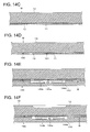
- FIG. 13 is a flowchart showing an example of a making procedure of the mechanical quantity sensor 100.
- FIG. 14A to FIG. 14K are cross-sectional views showing states of the mechanical quantity sensor 100 (corresponding to a cross section of the mechanical quantity sensor 100 taken along a line C-C in FIG. 1 ) during the making procedure in FIG. 13 .
- FIG. 14A to FIG. 14K correspond to upside-down arrangements of the mechanical quantity sensor 100 of FIG. 11 .
- FIG. 14A there is prepared a semiconductor substrate W formed by stacking three layers, first, second, and third layers 11, 12, 13.
- the first, second, and third layers 11, 12, 13 are layers for forming the first structure 110, the joining part 120, the second structure 130 respectively, and here they are formed of silicon containing impurities, a silicon oxide, and silicon containing impurities.
- the semiconductor substrate W having a stack structure of the three layers of silicon containing impurities/silicon oxide/silicon containing impurities can be made by joining a substrate obtained by stacking a silicon oxide film on a silicon substrate containing impurities and a silicon substrate containing impurities, and thereafter polishing the latter silicon substrate containing impurities to make it thin (what is called an SOI substrate).
- the silicon substrate containing impurities can be manufactured by, for example, doping boron during manufacturing of a silicon single crystal by a Czochralski method.
- An example of the impurities contained in the silicon is boron.
- the silicon containing boron for example, one containing high-concentration boron and having resistivity of 0.001 ⁇ cm to 0.01 ⁇ cm can be used.
- first layer 11 and the third layer 13 are formed of the same material (silicon containing impurities), but the first, second, and third layers 11, 12, 13 may all be formed of different materials.
- the first layer 11 is etched to form an opening 115, and form the first structure 110. That is, using an etching method which can erode the first layer 11 but does not erode the second layer 12, predetermined areas (openings 115a to 115d) of the first layer 11 is etched in a thickness direction until an upper face of the second layer 12 is exposed.
- a resist layer having a pattern corresponding to the first structure 110 is formed on an upper face of the first layer 11, and exposed portions not covered by this resist layer are eroded downward vertically.
- the second layer 12 is not eroded, and only the predetermined areas (openings 115a to 115d) of the first layer 11 are removed.
- FIG. 14B shows a state that the first layer 11 is etched as described above to form the first structure 110.
- the second layer 12 is etched to thereby form the joining part 120. Specifically, the second layer 12 is etched from its exposed portions in the thickness direction and a layer direction, by an etching method which can erode the second layer 12 but does not erode the first layer 11 and the third layer 13.
- the first structure 110 being a residue portion of the first layer 11 functions as a resist layer for the second layer 12.
- the etching is performed on an exposed portion of the second layer 12.
- the etching step (Step S12) on the second layer 12 it is necessary to perform an etching method that satisfies the following two conditions.
- the first condition is to have directions in the thickness direction as well as the layer direction.
- the second condition is that it can erode a silicon oxide layer but cannot erode a silicon layer.
- the first condition is a condition necessary for not allowing the silicon oxide layer to remain on an unnecessary portion and inhibit freedom of displacement of the weight portion 132.
- the second condition is a condition necessary for not allowing the erosion to reach the first structure 110, on which processing to make a predetermined shape is already completed, and the third layer 13, which are formed of silicon.
- the conduction portions 160 to 162 are formed as a, b below.
- Predetermined positions of the first structure 110 and the second layer 12 are wet etched, and weight-shaped through holes penetrating up to the second layer 12 are formed.
- a 20% TMAH tetramethylammonium hydroxide
- HF 5.5 wt%
- NH 4 F 20 wt
- A1 for example is deposited by a vapor deposition method, a sputtering method, or the like, so as to form the conduction portions 160 to 162.
- Unnecessary metal layers (metal layers outside edges (not shown) of upper ends of the conduction portions 160 to 162) deposited on the upper face of the first structure 110 are removed by etching.
- a substrate formed of an insulating material, for example, a glass substrate is etched to form the recessed portion 143, and then the driving electrode 144a, the detection electrodes 144b to 144e, and the wiring layers L1, L4 to L7 are formed at predetermined positions by a pattern formed of Al containing Nd for example.
- the semiconductor substrate W and the first base 140 are joined by anodic bonding for example.
- the first base 140 is anodically bonded before making the second structure 130. Since the first base 140 is anodically bonded before forming the weight portion 132, no thin area exists in the connection portions 113a to 113d, and thus they do not have flexibility. Thus, the displaceable portion 112 is not attracted to the first base 140 when electrostatic attraction occurs. Accordingly, joining of the first base 140 and the displaceable portion 112 can be prevented.
- FIG. 14E shows a state that the semiconductor substrate W and the first base 140 are joined.
- the second structure 130 is made as a to c below.
- the third layer 13 On the upper face of the third layer 13 excluding the formation area for the weight portion 132 and its vicinity, a resist layer is formed, and an exposed portion (formation area for the weight portion 132 and its vicinity) not covered by this resist layer is eroded downward vertically. As a result, the gap 10 for allowing the weight portion 132 to be displaced is formed above the area where the weight portion 132 is to be formed.
- projections 170 are formed at predetermined positions on an upper face of the area where the weight portion 132 is formed.
- Metal layers for example, a Cr layer and an Au layer are formed in this order by a vapor deposition method, a sputtering method, or the like on the upper face of the area where the weight portion 132 is formed. Unnecessary metal layers (metal layers outside the projections 170) are removed by etching, thereby forming the projections 170.
- the weight portion 132 is attracted and joined to the second base 150 by electrostatic attraction and adhering thereto, and the weight portion 132 does not operate, resulting in a state of not functioning as the mechanical quantity sensor 100.
- Providing the projections 170 allows to suppress adhesion of the weight portion 132 to the second base 150 even when the weight portion 132 is attracted to the second base 150 by electrostatic attraction, when the second base 150 and the second structure 130 are anodically bonded. This is because, when the projections 170 are provided, the contact area with respect to the second base 150 is smaller as compared to when the projections 170 are not provided.
- the tips of the projections 170 are formed of metal such as Au or the like which is difficult to be oxidized, it is possible to prevent adhesion of the weight portion 132 and the projections 170 to the second base 150 even when the weight portion 132 is attracted to the second base 150 by electrostatic attraction, when the second base 150 and the second structure 130 are anodically bonded. This is because it is possible to prevent coupling and adhesion of oxygen atoms of the glass (SiO 2 ) forming the second base 150 to the projections 170.
- the third layer 13 in which the projections 170 are formed is etched to form the opening 133, the block lower layer portions 134a to 134j, and the pocket 135, thereby forming the second structure 130.
- a predetermined area (opening 133) of the third layer 13 is etched in the thickness direction by an etching method that erodes the third layer 13 and does not erode the second layer 12.
- a resist layer having a pattern corresponding to the second structure 130 is formed on the upper face of the third layer 13, and an exposed portion not covered by this resist layer is eroded downward vertically.
- FIG. 14H shows a state that the second structure 130 is formed by etching the third layer 13 as described above.
- Step S11 it is necessary to perform an etching method as follows in the step of forming the first structure 110 (Step S11), and the step of forming the second structure 130 (Step S15).
- a first condition is to have directions in the thickness direction of each layer.
- a second condition is that it erodes a silicon layer but does not erode a silicon oxide layer.
- An etching method satisfying the first condition is ICP etching method (Inductively-Coupled Plasma Etching Method). This etching method is effective for opening a deep trench in a vertical direction, and is a kind of etching method that is generally called DRIE (Deep Reactive Ion Etching).
- ICP etching method Inductively-Coupled Plasma Etching Method
- DRIE Deep Reactive Ion Etching
- an etching stage of digging while eroding a material layer in a thickness direction and a deposition stage of forming a polymer wall on a side face of the dug hole are repeated alternately.
- the side face of the dug hole is protected by a polymer wall that is formed sequentially, and thus it becomes possible to allow the erosion to proceed almost only in the thickness direction.
- an etching material having etching selectivity between a silicon oxide and silicon may be used.
- a mixed gas of SF 6 gas and O 2 gas in the etching stage and use a C 4 F 8 gas in the deposition stage.
- the driving electrode 154a, the detection electrodes 154b to 154e, and the wiring layers L2, L8 to L11 are formed at predetermined positions with a pattern formed of A1 containing Nd for example. Further, the second base 150 is etched to form 11 truncated conical through holes 10 for forming the wiring terminals T1 to T11 at predetermined positions.
- a getter material (made by, for example, SAES Getters Japan, product name: Non-evaporable Getter St122) is put in the pocket 135, and the second base 150 and the semiconductor substrate W are joined by anodic bonding for example.
- the projections 170 having tips formed of, for example, metal such as Au which is difficult to be oxidized are provided. Accordingly, as described above, it is possible to prevent adhesion of the weight portion 132 and the projections 170 to the second base 150 even when the weight portion 132 is attracted to the second base 150 by electrostatic attraction, when the second base 150 and the second structure 130 are anodically bonded.
- FIG. 14I shows a state that the semiconductor substrate W and the second base 150 are joined.
- Metal layers for example, a Cr layer and an Au layer are formed in this order by a vapor deposition method, a sputtering method, or the like on the upper face of the second base 150 and in the conical through holes 10. Unnecessary metal layers (metal layers outside edges of upper ends of the wiring terminals T) are removed by etching, thereby forming the wiring terminals T1 to T11.
- the getter material in the pocket 135 is activated by, for example, heat treatment at 400°C, and thereafter the semiconductor substrate W, the first base 140, and the second base 150 joined together are cut by a dicing sawor the like, to thereby separate theminto individual mechanical quantity sensors 100.
- the mechanical quantity sensor 100 as above has the entire bodies or tips of the projections 170 being formed of, for example, metal such as Au, Pt or the like which is difficult to be oxidized.
- the projections may be formed of, for example, an insulating material such as a silicon oxide or a silicon nitride.
- FIG. 15 is a partial cross-sectional view showing a main part of a mechanical quantity sensor according to this modification example.
- the mechanical quantity sensor according to this modification example has projections 170a formed of an insulating material such as a silicon oxide or a silicon nitride for example on the upper face of the weight portion 132a.
- Providing the projections 170a allows to suppress adhesion of the weight portion 132 and the projections 170a to the second base 150 even when the weight portion 132 is attracted to the second base 150 by electrostatic attraction, when the second base 150 and the second structure 130 are anodically bonded. That is, the projections 170a function as adhesion preventing parts with respect to the second base 150.
- the projections 170a are arranged in the areas corresponding to areas, on the rear face of the weight portion 132 facing the second base 150, where the driving electrode 154a and the detection electrodes 154b to 154e are not arranged.
- the reason that the projections 170a are provided in the areas corresponding to the areas where the driving electrode 154a and the detection electrodes 154b to 154e are not arranged is to prevent, when the second base 150 and the second structure 130 are anodically bonded, the projections 170a from being pressed onto the driving electrode 154a and the detection electrodes 154b to 154e by electrostatic attraction, sinking into them and adhering thereto.
- projections 170 of the first embodiment shown in FIG. 6 there are provided four projections 170a in total according to this modification example on the rear face of the weight portion 132a, one by one in the areas corresponding to spaces between the driving electrode 154a and the detection electrodes 154b to 154e, respectively.
- the shape of the projections 170a can be, for example, a substantially rectangular parallelepiped, but it is not limited to a rectangular parallelepiped and may be of any shape. It is preferable that the heights of the projections 170a are thicker than thicknesses of the driving electrode 154a and the detection electrodes 154b to 154e so that they adequately function as adhesion preventing parts, and it can be 1 ⁇ m for example.
- the projections 170a formed of an insulating material such as a silicon oxide or a silicon nitride as the adhesion preventing parts when the weight portion 132 is attracted to the second base 150 by electrostatic attraction when the second base 150 and the second structure 130 are anodically bonded.
- FIG. 16 is a view showing a state that the weight portion 132 is attracted to the second base 150 by electrostatic attraction when the second base 150 and the second structure 130 are anodically bonded, and a projection 170a is in contact with the second base 150.
- a negative space-charge layer 180 is formed in the vicinity of the surface on the side close to the weight portion 132 of the second base 150.
- the projection 170a can be assumed as a capacitor C1, the space-charge layer 180 as a capacitor C2, and the second base 150 as a resistor R, and thus the structure in FIG. 16 can be represented by an equivalent circuit shown in FIG. 17 in which the resistor R and the two capacitors C1, C2 are connected in series.
- C ⁇ r ⁇ 0 (S/d) is the capacitance of a capacitor
- V 0 is applied voltage
- ⁇ r is a relative dielectric constant
- ⁇ 0 is a dielectric constant in vacuum
- S is a cross-sectional area of the projection 170a
- d is the height of the projection 170a (equal to the distance between the weight portion 132 and the second base 150 in FIG. 16 ).
- Attraction F between electrodes of the capacitor C1 is expressed by the following equation (2).
- F - ( d ⁇ / dx ⁇ )
- the electrostatic attraction working on the weight portion 132 and the second base 150 is in inverse proportion to the square of the height d of the projection 170a. Accordingly, even when the weight portion 132 is attracted to the second base 150 by electrostatic attraction during anodic bonding, the distance between the weight portion 132 and the second base 150 can be made large by providing the projection 170a, and thus the electrostatic attraction can be reduced.
- the projection 170a formed of an insulating material such as a silicon oxide, a silicon nitride, or the like functions as an adhesion preventing part that suppresses adhesion of the weight portion 132 and the projection 170a to the second base 150 during anodic bonding.
- the projections 170 in step S15 instead of making the projections 170 in step S15 (forming the second structure 130) in the method of making the mechanical quantity sensor 100 in the first embodiment, the projections 170a formed of an insulating material such as a silicon oxide, silicon nitride, or the like will be made.
- a silicon nitride layer is formed by a CVD method for example on the upper face of the area where the weight portion 132 is formed, and the projections 170a are formed by RIE (Reactive Ion Etching) with a resist being a mask.
- RIE Reactive Ion Etching
- FIG. 18 is an exploded perspective view showing a state that a mechanical quantity sensor 200 according to a second embodiment of the present invention is disassembled.
- FIG. 19 is a cross-sectional view taken along a line D-D in FIG. 18 . Parts common to FIG. 1 and FIG. 11 are given the same reference numerals, and overlapping descriptions are omitted.
- the mechanical quantity sensor 200 of this embodiment is different from the mechanical quantity sensor 100 of the first embodiment in the following points.
- wiring terminals T1a to T11a are formed in a first base 240 instead of the wiring terminals T1 to T11 formed in the second base 150 of the mechanical quantity sensor 100 in the first embodiment.
- the conduction portions 262 are provided in the block upper layer portions 114c, 114d, 114g, 114h, 114j instead of the conduction portions 162 formed in the block upper layer portions 114a, 114b, 114e, 114f, 114i of the mechanical quantity sensor 100 in the first embodiment.
- the conduction portions 262 establish conduction between the block upper layer portions 114c, 114d, 114g, 114h, 114 j and the block lower layer portions 134c, 134d, 134g, 134h, 134 j respectively, and penetrate the block upper layer portions 114c, 114d, 114g, 114h, 114j and the joining part 123 respectively.
- the structures of the conduction portions 262 are the same as those of the conduction portions 160 to 162 in the first embodiment.
- the first base 240 is formedof, for example, a glass material, has a substantially parallelepiped outer shape, and has a frame portion 241 and a bottom plate portion 242.
- the frame portion 241 and the bottom plate portion 242 can be made by forming a recessed portion 243 in a substantially rectangular parallelepiped shape (for example, 2.5 mm square and 5 ⁇ m deep) in a substrate.
- the wiring terminals Ta (T1a to T11a) are provided penetrating the frame portion 241 and the bottom plate portion 242, allowing electrical connections from the outside of the mechanical quantity sensor 200 to the driving electrodes 144a, 154a and the detection electrodes 144b to 144e, 154b to 154e.
- the structures of the wiring terminals T1a to T11a are the same as those of the wiring terminals T1 to T11 in the first embodiment.
- a lower end of the wiring terminal T1a is connected to an upper face of the projecting portion 111b of the fixed portion 111.
- Lower ends of the wiring terminals T2a to T9a are connected to upper faces of the block upper layer portions 114a to 114h, respectively (the numerical order of T2a to T9a of the wiring terminals T2a to T9a corresponds to the alphabetical order of 114a to 114h of the block upper layer portions 114a to 114h, respectively).
- the wiring terminals T10a, T11a are connected to upper faces of the block upper layer portions 114i, 114j, respectively.
- the wiring terminals T2a to T11a are connected electrically to the detection electrodes 144e, 144b, 154b, 154c, 144c, 144d, 154d, 154e, and the driving electrodes 144a, 154a, in order respectively.
- the wiring terminal T1a is connected electrically to the electrodes E1 formed in the upper face of the displaceable portion 112 and the lower face of the weight portion 132.
- a negative space-charge layer is formed in the vicinity of the surface on the side close to the weight portion 132 of the second base 250.
- the driving electrode 154a and the detection electrodes 154b to 154e are connected electrically to external grounds (grounded) via the wiring terminals T11a, T4a, T5a, T8a, T9a connected electrically to the driving electrode 154a and the detection electrodes 154b to 154e, respectively.
- These grounded driving electrode 154a and detection electrodes 154b to 154e cover the negative space-charge layer formed in the vicinity of the surface of the second base 250, and thus function as a shield layer which blocks an electrostatic force. Accordingly, when the second base 250 is anodically bonded, electrostatic attraction working on the lower face of the weight portion 132 and the upper face of the second base 250 can be reduced, and thus it is possible to suppress adherence of the weight portion 132 and the projections 170 to the second base 250.
- the projections 170 are provided in the areas corresponding to areas on the rear face of the weight portion 132 where the driving electrode 154a and the detection electrodes 154b to 154e are not arranged. Accordingly, as described above, it is possible to suppress adherence of the weight portion 132 and the projections 170 to the second base 150 even when the weight portion 132 is attracted to the second base 150 by electrostatic attraction when the second base 150 and the second structure 130 are anodically bonded.
- projections 170 instead of the projections 170 with entire bodies or tips being formed of, for example, metal such as Au, Pt, or the like which is difficult to be oxidized, it is possible to provide projections 170a formed of an insulating material such as a silicon oxide, a silicon nitride, or the like.
- the driving electrode 154a and the detection electrodes 154b to 154e can be made to function as a shield layer when the second base 250 is anodically bonded, and moreover, the projections 170 provided on the rear face of the weight portion 132 can be made to function as joining preventing parts. Accordingly, with the mechanical quantity sensor 200 and the method of manufacturing the same, it is possible to more reliably suppress adhesion of the weight portion 132 and the projections 170 to the second base 250 when the second base 250 is anodically bonded.
- the driving electrode 144a and the detection electrodes 144b to 144e are connected electrically to external grounds (grounded) via the wiring terminals T10a, T3a, T6a, T7a, T2a connected electrically to the driving electrode 144a and the detection electrodes 144b to 144e, respectively. Accordingly, even when a negative space-charge layer is formed in the vicinity of the surface of the first base 240, the driving electrode 144a and the detection electrodes 144b to 144e cover the surface of the first base 240, and thus function as a shield layer which blocks an electrostatic force.
- the wiring terminal T1a electrically connected to the weight portion 132 and the wiring terminals T2a to T11a electrically connected to the driving electrodes 144a, 154a and the detection electrodes 144b to 144e, 154b to 154e are connected electrically on the outside via conducting wires or the like.
- the driving electrode 144a and the detection electrodes 144b to 144e arranged on the upper face of the first base 240 and the upper face of the displaceable portion 112 are electrically connected on the outside via conducting wires or the like.
- electrical conduction is established between the driving electrode 144a and the detection electrodes 144b to 144e and the upper face of the displaceable portion 112, and thus they have equal potentials.
- No electrostatic attraction works between the driving electrode 144a and the detection electrodes 144b to 144e and the upper face of the displaceable portion 112, which have equal potentials.
- adhesion of the displaceable portion 112 to the first base 240 can further be suppressed when the second base 250 is anodically bonded.
- FIG. 20 is a flowchart showing an example of a making procedure of the mechanical quantity sensor 200.
- the method of making the mechanical quantity sensor 200 of this embodiment is different from the method of making the mechanical quantity sensor 100 of the first embodiment in the following points.
- the wiring terminals T1a to T11a are formed in the second base 240 in step 25, instead of forming the wiring terminals T1 to T11 on the second base 150 in step 17 in the method of making the mechanical quantity sensor 100 in the first embodiment.
- the wiring terminals T2a to T11a electrically connected to the driving electrodes 144a, 154a and the detection electrodes 144b to 144e, 154b to 154e are connected electrically to external grounds (grounded).
- the wiring terminal T1a connected electrically to the weight portion 132 and the wiring terminals T2a to T11a connected electrically to the driving electrodes 144a, 154a and the detection electrodes 144b to 144e, 154b to 154e are electrically connected on the outside via conducting wires or the like.
- step 28 the conducting wires for example which connect the wiring terminal T1a and the wiring terminals T2a to T11a on the outside of the mechanical quantity sensor 200 are removed.
- the driving electrode 154a and the detection electrodes 154b to 154e are grounded and made to function as a shield layer when the second base 250 is anodically bonded. Further, the projections 170 are provided and made to function as joining preventing parts in the areas corresponding to areas on the rear face of the weight portion 132 where the driving electrode 154a and the detection electrodes 154b to 154e are not arranged.
- the areas of the driving electrode 154a and the detection electrodes 154b to 154e which function as a shield layer may be made larger than in the second embodiment, so as to make a smaller sum total of areas of gaps of the driving electrode 154a and the detection electrodes 154b to 154e as a result.
- the electrostatic attraction working between the weight portion 132 and the second base 250 can be made smaller when the second base 250 is anodically bonded, and thus it is possible to suppress adhesion of the weight portion 132 to the second base 250.
- Embodiments of the present invention are not limited to the above-described embodiments and can be extended and modified. Extended and modified embodiments are included in the technical scope of the present invention.
- the mechanical quantity sensors 100, 200 are described with examples of using a conductive material (silicon containing impurities) for the first structure 110 and the second structure 130 (except the projections 170), but it is not always necessary that the entire body is formed of the conductive material. It may be arranged that at least necessary parts, such as the driving electrodes E1, the detection electrodes E1, parts establishing conduction between the wiring terminal T10 and the upper face of the block upper layer portion 114i, and the like, are formed of the conductive material.
- a conductive material silicon containing impurities
Abstract
Description
- The present invention relates to a mechanical quantity sensor detecting a mechanical quantity and a method of manufacturing the same.
- There has been disclosed a technique of an angular velocity sensor, which is structured such that a transducer structure formed of a semiconductor is sandwiched by a pair of glass substrates and joined thereto, for detecting an angular velocity (see Reference 1).
- Reference 1:
JP-A 2002-350138 - However, it has been found that when a glass substrate is anodically bonded to the side of the transducer structure where a movable weight (weight portion) is arranged, it is possible that the weight is attracted to the glass substrate by electrostatic attraction and adheres thereto, and it no longer functions as an angular velocity sensor. Considering this situation, an object of the present invention is to provide a mechanical quantity sensor and a method of manufacturing the same, capable of preventing adhesion of the weight (weight portion) to the glass substrate when the transducer structure formed of a semiconductor and the glass substrate are anodically bonded.
- A mechanical quantity sensor according to an aspect of the present invention includes: a first structure having a fixed portion with an opening, a displaceable portion arranged in the opening and displaceable relative to the fixed portion, and a connection portion connecting the fixed portion and the displaceable portion, the first structure being formed of a first semiconductor material in a plate shape; a second structure having a weight portion joined to the displaceable portion and a pedestal arranged surrounding the weight portion and joined to the fixed portion, the second structure being formed of a second semiconductor material and arranged and stacked on the first structure; a first base connected to the fixed portion, arranged and stacked on the first structure, and formed of an insulating material; and a second base having a driving electrode applying vibration in a stacking direction to the displaceable portion, arranged on a face facing the weight portion, and formed of a conductive material, and a detection electrode detecting a displacement of the displaceable portion, arranged on a face facing the weight portion, and formed of a conductive material, the second base formed of an insulating material, connected to the pedestal, and arranged and stacked on the second structure, in which the second structure has a projection arranged in an area on a face of the weight portion facing the second base, the area corresponding to an area where the driving electrode and the detection electrode are not arranged, the projection having a thickness larger than thicknesses of the driving electrode and the detection electrode.
- A method of manufacturing a mechanical quantity sensor according to an aspect of the present invention includes: forming a first structure having a fixed portion with an opening, a displaceable portion arranged in the opening and displaceable relative to the fixed portion, and a connection portion connecting the fixed portion and the displaceable portion, by etching a first layer of a semiconductor substrate formed by sequentially stacking the first layer formed of a first semiconductor material, a second layer formed of an insulating material, and a third layer formed of a second semiconductor material; arranging and stacking a first base formed of an insulating material on the first structure by joining the first base to the fixed portion; forming a second structure having a weight portion joined to the displaceable portion, a projection arranged on a face of the weight portion on a side opposite to a face joined to the displaceable portion or on a face of an area of the third layer where the weight portion is to be formed on a side opposite to a face joined to the displaceable portion, and a pedestal arranged surrounding the weight portion and joined to the fixed portion, by etching the third layer; and arranging and stacking a second base on the second structure by anodically bonding the second base to the pedestal, the second base formed of an insulating material and having a first driving electrode arranged on a face facing the weight portion, formed of a conductive material, and applying vibration in a stacking direction to the displaceable portion, and a first detection electrode arranged on a face facing the weight portion, formedof aconductivematerial, anddetectingadisplacement of the displaceable portion, in which the projection is arranged in an area corresponding to an area where the first driving electrode and the first detection electrode are not arranged, and has a thickness larger than thicknesses of the first driving electrode and the first detection electrode.
-
- [
FIG. 1] FIG. 1 is an exploded perspective view showing a state that a mechanical quantity sensor according to a first embodiment of the present invention is disassembled. - [
FIG. 2] FIG. 2 is an exploded perspective view showing a state that the mechanical quantity sensor inFIG. 1 is disassembled. - [
FIG. 3] FIG. 3 is a top view of a first structure. - [
FIG. 4] FIG. 4 is a top view of a joining part. - [
FIG. 5] FIG. 5 is a top view of a second structure. - [
FIG. 6] FIG. 6 is a bottom view of the second structure. - [
FIG. 7] FIG. 7 is a bottom view of a first base. - [
FIG. 8] FIG. 8 is a top view of a second base. - [
FIG. 9] FIG. 9 is a bottom view of the second base. - [
FIG. 10] FIG. 10 is a cross-sectional view taken along a line B-B inFIG. 1 . - [
FIG. 11] FIG. 11 is a cross-sectional view taken along a line C-C inFIG. 1 . - [
FIG. 12] FIG. 12 is a cross-sectional view showing six pairs of capacitor elements in the mechanical quantity sensor shown inFIG. 10 . - [
FIG. 13] FIG. 13 is a flowchart showing an example of a making procedure of the mechanical quantity sensor according to the first embodiment of the present invention. - [
FIG. 14A] FIG. 14A is a cross-sectional view showing a state of the mechanical quantity sensor in the making procedure inFIG. 13 . - [
FIG. 14B] FIG. 14B is a cross-sectional view showing a state of the mechanical quantity sensor in the making procedure inFIG. 13 . - [
FIG. 14C] FIG. 14C is a cross-sectional view showing a state of the mechanical quantity sensor in the making procedure inFIG. 13 . - [
FIG. 14D] FIG. 14D is a cross-sectional view showing a state of the mechanical quantity sensor in the making procedure inFIG. 13 . - [
FIG. 14E] FIG. 14E is a cross-sectional view showing a state of the mechanical quantity sensor in the making procedure inFIG. 13 . - [
FIG. 14F] FIG. 14F is a cross-sectional view showing a state of the mechanical quantity sensor in the making procedure inFIG. 13 . - [
FIG. 14G] FIG. 14G is a cross-sectional view showing a state of the mechanical quantity sensor in the making procedure inFIG. 13 . - [
FIG. 14H] FIG. 14H is a cross-sectional view showing a state of the mechanical quantity sensor in the making procedure inFIG. 13 . - [
FIG. 14I] FIG. 14I is a cross-sectional view showing a state of the mechanical quantity sensor in the making procedure inFIG. 13 . - [
FIG. 14J] FIG. 14J is a cross-sectional view showing a state of the mechanical quantity sensor in the making procedure inFIG. 13 . - [
FIG. 14K] FIG. 14K is a cross-sectional view showing a state of the mechanical quantity sensor in the making procedure inFIG. 13 . - [
FIG. 15] FIG. 15 is a partial cross-sectional view showing a main part of the mechanical quantity sensor according to a modification example. - [
FIG. 16] FIG. 16 is a view showing a state that a weight portion is attracted to the second base by electrostatic attraction and a projection and the second base are in contact, when the second base and the second structure are anodically bonded. - [
FIG. 17] FIG. 17 is an explanatory diagram showing the principle of functioning of a projection formed of an insulating material as an adhesion preventing part. - [
FIG. 18] FIG. 18 is an exploded perspective view showing a state that a mechanical quantity sensor according to a second embodiment of the present invention is disassembled. - [
FIG. 19] FIG. 19 is a cross-sectional view taken along a line D-D inFIG. 18 . - [
FIG. 20] FIG. 20 is a flowchart showing an example of a making procedure of the mechanical quantity sensor according to the second embodiment of the present invention. - 100, 200...mechanical quantity sensor; 110... first structure; 111... fixed portion; 111a... frame portion; 111b, 111c... projecting portion; 112 (112a - 112e)... displaceable portion; 113 (113a - 113d)... connection portion; 114 (114a - 114j)... block upper layer portion; 115 (115a - 115d)... opening; 120, 121, 122, 123... joining part; 130... second structure; 131... pedestal; 131a... frame portion; 131b - 131d... projecting portion; 132 (132a - 133e)... weight portion; 133... opening; 134 (134a - 134j)... block lower layer portion; 135... pocket; 140, 240... first base; 141... frame portion; 142... bottom plate portion; 143... recessed portion; 144a... driving electrode; 144b - 144e... detection electrode; 150, 250... second base; 154a... driving electrode; 154b - 154e... detection electrode; 160 - 162, 262... conduction portion; 170, 170a...projection; 180... space-charge layer; 10... gap; 11... weight-shaped through hole; L1, L2, L4-L11... wiring layer; T1 - T11 ... wiring terminal; E1... driving electrode, detection electrode
- Hereinafter, embodiments of the present invention will be described in detail with reference to the drawings.
-
FIG. 1 is an exploded perspective view showing a state that amechanical quantity sensor 100 is disassembled. Themechanical quantity sensor 100 has afirst structure 110, a joiningpart 120, and asecond structure 130 which are stacked one another, and afirst base 140 and asecond base 150. -
FIG. 2 is an exploded perspective view showing a state that part (first structure 110 and second structure 130) of themechanical quantity sensor 100 is further disassembled.FIG. 3, FIG. 4 ,FIG. 5 , andFIG. 6 are a top view of thefirst structure 110, a top view of the joiningpart 120, a top view of thesecond structure 130, and a bottom view of the second structure, respectively.FIG. 7, FIG. 8 , andFIG. 9 are a bottom view of thefirst base 140, a top view of thesecond base 150, and a bottom view of thesecond base 150, respectively.FIG. 10 andFIG. 11 are cross-sectional views of themechanical quantity sensor 100 taken along a line B-B and a line C-C ofFIG. 1 . - The
mechanical quantity sensor 100 functions by itself or in combination with a circuit board (for example, mounted on a board) as an electronic component. Themechanical quantity sensor 100 as an electronic component can be mounted in a game machine, a mobile terminal (for example, a cellular phone), or the like. In addition, themechanical quantity sensor 100 and the circuit board (active elements such as IC and wiring terminals on the circuit board) are connected electrically by wire bonding, flip-chip bonding, or the like. - The
mechanical quantity sensor 100 is capable of measuring one or both of an acceleration α and an angular velocity ω. That is, a mechanical quantity means one or both of the acceleration α and the angular velocity ω. Accelerations αx, αy, αz can be measured by detecting displacements of a displaceable portion 112 (which will be described later) caused by forces F0x, F0y, F0z in X, Y, Z-axis directions, respectively. Further, angular velocities ωx, ωy in X, Y-axis directions respectively can be measured by vibrating the displaceable portion 112 in the Z-axis direction and detecting displacements of the displaceable portion 112 caused by Coriolis forces Fy, Fx in Y, X-axis directions, respectively. In this manner, themechanical quantity sensor 100 is capable of measuring the accelerations αx, αy, αz in three axes and the angular velocities ωx, ωy in two axes. Note that details of this will be described later. - The
first structure 110, the joiningpart 120, thesecond structure 130, thefirst base 140, and thesecond base 150 each have a substantially square outer periphery with each side being 5 mm for example, and have heights of, for example, 20 µm, 2 µm, 675 µm, 500 µm, and 500 µm, respectively. - The
first structure 110, the joiningpart 120, and the second structure 130 (excludingprojections 170 which will be described later) can be formed of silicon, silicon oxide, and silicon, respectively, and themechanical quantity sensor 100 can be manufactured using an SOI (Silicon On Insulator) substrate forming a three-layer structure of silicon/silicon oxide/silicon. For the silicon forming thefirst structure 110 and the second structure 130 (excluding projections 170), it is preferable to use a conductive material containing impurities, for example boron or the like, in its entirety. As will be described later, use of silicon containing impurities for forming thefirst structure 110 and the second structure 130 (excluding projections 170) allows to simplify wiring of themechanical quantity sensor 100. In this embodiment, silicon containing impurities is used for thefirst structure 110 and the second structure 130 (excluding projections 170). - Further, the
first base 140 and thesecond base 150 can each be formed of a glass material. - The
first structure 110 has a substantially square outer shape, and is made up of a fixed portion 111 (111a to 111c), a displaceable portion 112 (112a to 112e), a connection portion 113 (113a to 113d), and a block upper layer portion 114 (114a to 114j). Thefirst structure 110 can be made by etching a film of a semiconductor material and formingopenings 114a to 114d and blockupper layer portions 114a to 114j. - The fixed portion 111 can be separated into a
frame portion 111a and projectingportions frame portion 111a is a frame-shaped substrate with an outer periphery and an inner periphery both being a substantially square. The projectingportion 111b is a substantially square substrate, arranged at a corner portion on the inner periphery of theframe portion 111a and projecting toward thedisplaceable portion 112b (in a 0° direction when an X direction of the X-Y plane is 0°). The projectingportion 111c is a substantially square substrate, arranged at a corner portion on the inner periphery of theframe portion 111a and projecting toward thedisplaceable portion 112d (in a 180° direction when an X direction of the X-Y plane is 0°). Theframe portion 111a and the projectingportions - The displaceable portion 112 is made up of
displaceable portions 112a to 112e. Thedisplaceable portion 112a is a substrate having a substantially square outer periphery and is arranged in the vicinity of the center of an opening of the fixed portion 111. Thedisplaceable portions 112b to 112e are substrates each having a substantially square outer periphery and are connected and arranged so as to surround thedisplaceable portion 112a from four directions (X-axis positive direction, X-axis negative direction, Y-axis positive direction, and Y-axis negative direction). Thedisplaceable portions 112a to 112e are joined respectively toweight portions 132a to 132e which will be described later by the joiningpart 120, and are displaced integrally relative to the fixed portion 111. - An upper face of the
displaceable portion 112a functions as a driving electrode E1 (which will be described later). Thedriving electrode E1 on the upper face of thedisplaceable portion 112a capacitively couples to a drivingelectrode 144a, which will be described later, disposed on a lower face of thefirst base 140, and the displaceable portion 112 is vibrated in the Z-axis direction by voltage applied therebetween. Note that details of this driving will be described later. - Upper faces of the
displaceable portions 112b to 112e each function as a detection electrode E1 (which will be described later) detecting displacements in the X-axis and Y-axis directions of the displaceable portion 112. The detection electrodes on the upper faces of thedisplaceable portions 112b to 112e capacitively couple respectively todetection electrodes 144b to 144e, which will be described later, disposed on a lower face of the first base 140 (the alphabets b to e of the displaceable portions 112 correspond to the alphabets b to e of the detection electrodes 144 in order respectively). Note that details of this detection will be described later. - The
connection portions 113a to 113d are substantially rectangular substrates connecting the fixed portion 111 and thedisplaceable portion 112a in four directions (45°, 135°, 225°, 315° directions when the X direction of the X-Y plane is 0°). - Areas of the
connection portions 113a to 113d close to theframe portion 111a are joined by the joiningpart 120 to projectingportions 131c of a pedestal 131 (which will be described later). For other areas of theconnection portions 113a to 113d, that is, areas close to thedisplaceable portion 112a, the projectingportions 131c are not formed in the corresponding areas, and these areas have a small thickness and hence have flexibility. The reason that the areas of theconnection portions 113a to 113d close to theframe portion 111a are joined to the projectingportions 131c is to prevent damage to theconnection portions 113a to 113d by large deflection. - The
connection portions 113a to 113d function as deflectable beams. Deflection of theconnection portions 113a to 113d can displace the displaceable portion 112 relative to the fixed portion 111. Specifically, the displaceable portion 112 is displaced linearly in a Z positive direction and a Z negative direction relative to the fixed portion 111. Further, the displaceable portion 112 is capable of rotating positively or negatively with the X-axis and Y-axis being rotation axes, relative to the fixed portion 111. That is, the "displacement" mentioned here can include both movement and rotation (movement in the Z-axis direction and rotation about the X, Y axes). - The block upper layer portion 114 is made up of block
upper layer portions 114a to 114j. The blockupper layer portions 114a to 114j are substantially square substrates and are arranged along the inner periphery of the fixed portion 111 so as to surround the displaceable portion 112 from its periphery. - The block
upper layer portions displaceable portion 112e, and the blockupper layer portions displaceable portion 112b. The blockupper layer portions displaceable portion 112c, and the blockupper layer portions displaceable portion 112d. As shown inFIG. 1 , the blockupper layer portions 114a to 114h each have the end face facing one of eight end faces of the displaceable portion 112, and are arranged clockwise in alphabetical order. The blockupper layer portion 114i and the blockupper layer portion 114j are arranged in 90°, 270° directions when the X direction of the X-Y plane is 0°. - The block
upper layer portions 114a to 114h are joined respectively to blocklower layer portions 134a to 134h, which will be described later, by the joining part 120 (the alphabets a to h of the block upper layer portions 114 correspond to the alphabets a to h of the blocklower layer portions 134 in order respectively). The blocks made by joining the blockupper layer portions 114a to 114h and the blocklower layer portions 134a to 134h, respectively, are used for the purpose of wiring for supplying power todetection electrodes 144b to 144e, 154b to 154e, which will be described later. - The block
upper layer portions lower layer portions part 120. The block made by joining the blockupper layer portions lower layer portions - The
second structure 130 has a substantially square outer shape, and is made up of a pedestal 131 (131a to 131d), a weight portion 132 (132a to 132e), a block lower layer portion 134 (134a to 134j), andprojections 170. Thesecond structure 130 can be made by etching a substrate of a semiconductor material to form anopening 133, blocklower layer portions 134a to 134j, and a pocket 135 (which will be described later), and forming theprojections 170 by sputtering and etching. In addition, thepedestal 131 and the blocklower layer portions 134a to 134j are substantially equal in height, and theweight portion 132 is lower in height than thepedestal 131 and the blocklower layer portions 134a to 134j. This is for securing a space (gap) between theweight portion 132 and thesecond base 150 for allowing theweight portion 132 to be displaced. Thepedestal 131, the blocklower layer portions 134a to 134j, and theweight portion 132 are arranged separately from each other. - The
pedestal 131 can be separated into aframe portion 131a and projectingportions 131b to 131d. - The
frame portion 131a is a frame-shaped substrate with an outer periphery and an inner periphery both being a substantially square, and has a shape corresponding to theframe portion 111a of the fixed portion 111. - The projecting
portion 131b is a substantially square substrate, arranged at a corner portion on the inner periphery of theframe portion 131a and projecting toward theweight portion 132b (in a 0° direction when the X direction of the X-Y plane is 0°), and has a shape corresponding to the projectingportion 111b of the fixed portion 111. - The projecting
portions 131c are four substantially rectangular substrates, projecting toward theweight portion 132a from theframe portion 131a in 45°, 135°, 225°, 315° directions respectively when the X direction of the X-Y plane is 0°, and having one ends connected to theframe portion 131a of thepedestal 131 and the other ends arranged separately from theweight portion 132a. The projectingportions 131c are formed in substantially half areas on theframe portion 131a side in the areas corresponding to theconnection portions 113a to 113d, and are not formed in other areas, that is, substantially half areas on theweight portion 132 side. - The projecting
portion 131d is a substantially square substrate, arranged at a corner portion on the inner periphery of theframe portion 131a and projecting toward theweight portion 132d (in the 180° direction when X direction of the X-Y plane is 0°), in which a pocket 135 (opening) penetrating through a front face and a rear face of this substrate is formed, and is joined to the projectingportion 111c of the fixed portion 111. - The
pocket 135 is a rectangular parallelepiped space for example, in which a getter material for maintaining a high vacuum is placed. One opening end of thepocket 135 is covered by the joiningpart 120. Most part of the other opening end of thepocket 135 is covered by thesecond base 150, but a part thereof near theweight portion 132 is not covered. This other opening end and theopening 133 in which theweight portion 132 and so on are formed communicate partly with each other (not shown). - The getter material absorbs a residue gas for the purpose of increasing the degree of vacuum in the
mechanical quantity sensor 100 which is vacuum sealed. This allows to reduce the effect of air resistance when the displaceable portion 112 (and the weight portion 132) vibrates. As the getter material used for themechanical quantity sensor 100, for example, a mixture of titanium and a Zr-V-Fe alloy (made by SAES Getters Japan, product name: Non-evaporable Getter St122) can be used. - The
frame portion 131a and the projectingportions 131b to 131d are formed integrally. - The
pedestal 131 is connected to the fixed portion 111 and predetermined areas of theconnection portions 113a to 113d by the joiningpart 120. - The
weight portion 132 functions as a heavy weight or an operating body having a mass and receiving the force F0 and the Coriolis force F caused by the acceleration α and the angular velocity ω respectively. That is, when the acceleration α and the angular velocity ω are applied, the force F0 and the Coriolis force F act on the center of gravity of theweight portion 132. - The
weight portion 132 is separated intoweight portions 132a to 132e having a rectangular parallelepiped shape. Theweight portions 132b to 132e are connected from four directions to theweight portion 132a arranged in the center, and are displaceable (movable, rotatable) integrally as a whole. That is, theweight portion 132a functions as a connection portion connecting theweight portions 132b to 132e. - The
weight portions 132a to 132e have substantially square cross-sectional shapes corresponding to thedisplaceable portions 112a to 112e, respectively, and are joined to thedisplaceable portions 112a to 112e by the joiningpart 120. The displaceable portion 112 is displaced according to the force F0 and the Coriolis force F applied to theweight portion 132, and consequently, it becomes possible to measure the acceleration α and the angular velocity ω. - The reason that the
weight portion 132 is made up of theweight portions 132a to 132e is to achieve both reduction in size and increase in sensitivity of themechanical quantity sensor 100. When themechanical quantity sensor 100 is reduced in size (reduced in capacity), the capacity of theweight portion 132 decreases, and its mass decreases, resulting in decreased sensitivity to the mechanical quantity. Dispersed arrangement of theweight portions 132b to 132e which does not hinder deflections of theconnection portions 113a to 113d assures the mass of theweight portions 132. Consequently, the reduction in size and the increase in sensitivity of themechanical quantity sensor 100 are both achieved. - A rear face of the
weight portion 132a functions as a driving electrode E1 (which will be described later). This driving electrode E1 on the rear face of theweight portion 132a capacitively couples to a drivingelectrode 154a, which will be described later, disposed on an upper face of thesecond base 150, and the displaceable portion 112 is vibrated in the Z-axis direction by voltage applied therebetween. Note that details of this driving will be described later. - Rear faces of the
weight portions 132b to 132e each function as a detection electrode E1 (which will be described later) detecting a displacement of the displaceable portion 112 in the X-axis and Y-axis directions. The detection electrodes E1 on the rear faces of theweight portions 132b to 132e capacitively couple respectively todetection electrodes 154b to 154e, which will be described later, disposed on the upper face of the second base 150 (the alphabets b to e of theweight portion 132 correspond to the alphabets b to e of the detection electrodes 154 in order respectively). Note that details of this detection will be described later. - The
projections 170 are arranged in the areas corresponding to areas on the rear face of theweight portion 132 where the drivingelectrode 154a and thedetection electrodes 154b to 154e, which will be described later, are not arranged. This arrangement is for preventing, when thesecond base 150 and thesecond structure 130 are anodically bonded, theweight portion 132 from being pressed onto the drivingelectrode 154a and thedetection electrodes 154b to 154e by electrostatic attraction, sinking into them and adhering thereto. - As shown in
FIG. 6 , in this embodiment, there are provided fourprojections 170 in total on the rear face of theweight portion 132a, one by one in the areas corresponding to spaces between the drivingelectrode 154a and thedetection electrodes 154b to 154e, respectively. - Conventionally, when the
second base 150 and thesecond structure 130 are anodically bonded (when the second glass substrate is anodically bonded), it is possible that theweight portion 132 is attracted and joined to thesecond base 150 by electrostatic attraction and adhering thereto, and theweight portion 132 does not operate, resulting in a state of not functioning as themechanical quantity sensor 100. - Providing the
projections 170 allows to suppress adhesion of theweight portion 132 and theprojections 170 to thesecond base 150 even when theweight portion 132 is attracted to thesecond base 150 by electrostatic attraction, when thesecond base 150 and thesecond structure 130 are anodically bonded. This is because, when theprojections 170 are provided, the contact area with respect to thesecond base 150 is smaller as compared to when theprojections 170 are not provided. That is, theprojections 170 function as adhesion preventing parts with respect to thesecond base 150. - As described above, the
projections 170 are arranged in the areas corresponding to the spaces between the electrodes 154 (drivingelectrode 154a anddetection electrodes 154b to 154e). That is, theprojections 170 are arranged corresponding to areas where the electrodes 154 are not provided. This provides the following advantages 1) and 2). - 1) When the
second base 150 and thesecond structure 130 are anodically bonded, adhesion of theweight portion 132 to thesecond base 150 is securely prevented. That is, adhesion of theprojections 170 to the electrodes 154 can be prevented. The electrodes 154 are formed of a relatively soft material such as metal, and thus when theprojections 170 are arranged facing the electrodes 154, it is possible that theprojections 170 sink into the electrodes 154 and adhere thereto. - 2) The
projections 170 do not easily affect signals on the electrodes 154. That is, changes of characteristics of themechanical quantity sensor 100 due to addition of theprojections 170 are prevented. When theprojections 170 are arranged facing the electrodes 154, it is possible to affect signals on the electrodes 154 as well as characteristics of themechanical quantity sensor 100. - It is preferable that the entire bodies or tips of the
projections 170 are formed of, for example, metal such as Au, Pt, or the like which is difficult to be oxidized. With the entire bodies or tips of theprojections 170 being formed of metal such as Au, Pt, or the like which is difficult to be oxidized, it is possible to prevent adhesion of theweight portion 132 and theprojections 170 to thesecond base 150 evenwhen theweight portion 132 is attracted to thesecond base 150 by electrostatic attraction, when thesecond base 150 and thesecond structure 130 are anodically bonded. This is because it is possible to prevent coupling and adhesion of oxygen atoms of the glass (SiO2) forming thesecond base 150 to theprojections 170. - The shape of the
projections 170 can be, for example, a substantially rectangular parallelepiped, but it is not limited to a rectangular parallelepiped and may be of any shape. It is preferable that the heights of theprojections 170 are thicker than thicknesses of the drivingelectrode 154a and thedetection electrodes 154b to 154e so that they adequately function as adhesion preventing parts, and it can be 1 µm for example. - The block
lower layer portions 134a to 134j have substantially square cross-sectional shapes corresponding to those of the blockupper layer portions 114a to 114j, respectively, and are joined to the blockupper layer portions 114a to 114j by the joiningpart 120. Blocks made by joining the blockupper layer portions 114a to 114h and the blocklower layer portions 134a to 134h are hereinafter referred to as "blocks a to h", respectively. The blocks a to h are used for the purpose of wirings to supply power todetection electrodes 144b to 144e, 154b to 154e, respectively. Blocks made by joining the blockupper layer portions lower layer portions - The joining
part 120 connects the first,second structures part 120 is separated into a joiningpart 121 connecting the predetermined areas of the connection portions 113 and the fixed portion 111 to thepedestal 131, a joining part 122 (122a to 122e) connecting thedisplaceable portions 112a to 112e to theweight portions 132a to 133e, and a joining part 123 (123a to 123j) connecting the blockupper layer portions 114a to 114j to the blocklower layer portions 134a to 134j. Other than these portions, the joiningpart 120 does not connect the first andsecond structures connection portions 113a to 113d to deflect and theweight portion 132 to be displaced. - In addition, the joining
parts -
Conduction portions 160 to 162 are formed for establishing conduction of thefirst structure 110 and thesecond structure 130 at necessary portions. - The
conduction portion 160 establishes conduction between the fixed portion 111 and thepedestal 131, and penetrates the projectingportion 111b of the fixed portion 111 and the joiningpart 121. - The
conduction portion 161 establishes conduction between the displaceable portion 112 and theweight portion 132, and penetrates thedisplaceable portion 112a and the joiningpart 122. - The
conduction portions 162 establish conduction between the blockupper layer portions lower layer portions upper layer portions part 123 respectively. - The
conduction portions 160 to 162 are made by forming, for example, metal layers of A1 or the like on, for example, edges, wall faces and bottom portions of through holes. In addition, although shapes of the through holes are not particularly limited, the through holes of theconduction portions 160 to 162 are preferred to be formed in truncated conical shapes because they allow to form metal layers effectively by sputtering or the like of A1 or the like. - The
first base 140 is formedof, for example, a glass material, has a substantially parallelepiped outer shape, and has aframe portion 141 and abottom plate portion 142. Theframe portion 141 and thebottom plate portion 142 can be made by forming a recessedportion 143 in a substantially rectangular parallelepiped shape (for example, 2.5 mm square and 5 µm deep) in a substrate. - The
frame portion 141 has a substrate shape that is a frame shape with an outer periphery and an inner periphery both being a substantially square. The outer periphery of theframe portion 141 matches the outer periphery of the fixed portion 111, and the inner periphery of theframe portion 141 is smaller than the inner periphery of the fixed portion 111. - The
bottom plate portion 142 has a substantially square substrate shape having an outer periphery that is substantially the same as that of theframe portion 141. - The reason that the recessed
portion 143 is formed in thefirst base 140 is to secure a space for allowing the displaceable portion 112 to be displaced. Thefirst structure 110 excluding the displaceable portion 112, that is, the fixed portion 111 and the blockupper layer portions 114a to 114j are joined to thefirst base 140 by anodic bonding for example. - On the bottom plate portion 142 (on a rear face of the first base 140), a driving
electrode 144a anddetection electrodes 144b to 144e are arranged so as to face the displaceable portion 112. The drivingelectrode 144a and thedetection electrodes 144b to 144e can all be formed of a conductive material. The drivingelectrode 144a is cross shaped for example and is formed in the vicinity of the center of the recessedportion 143 so as to face thedisplaceable portion 112a. Thedetection electrodes 144b to 144e each have a substantially square shape, surrounding the drivingelectrode 144a from four directions (the X-axis positive direction, the X-axis negative direction, the Y-axis positive direction, and the Y-axis negative direction), and are arranged to face thedisplaceable portions 112b to 112e in order respectively. The drivingelectrode 144a and thedetection electrodes 144b to 144e are separated from each other. - A wiring layer L1 electrically connected to an upper face of the block
upper layer portion 114i is connected to the drivingelectrode 144a. Awiring layer L4 electrically connected to an upper face of the blockupper layer portion 114b is connected to thedetection electrode 144b. Awiring layer L5 electrically connected to an upper face of the blockupper layer portion 114e is connected to thedetection electrode 144c. Awiring layer L6 electrically connected to an upper face of the blockupper layer portion 114f is connected to thedetection electrode 144d. Awiring layer L7 electrically connected to an upper face of the blockupper layer portion 114a is connected to thedetection electrode 144e. - As a constituent material for the driving
electrode 144a, thedetection electrodes 144b to 144e, and the wiring layers L1, L4 to L7, Al containing Nd can be used for example. - Use of the A1 containing Nd for the driving
electrode 144a, thedetection electrodes 144b to 144e, and the like allows to suppress formation of hillocks on the drivingelectrode 144a, thedetection electrodes 144b to 144e, and the like during a heat treatment process (anodic bonding of thefirst base 140 or thesecond base 150 and activation of the getter material) which will be described later. The hillocks mentioned here are, for example, hemispheric projections. Thus, dimensional accuracy can be increased for a distance between the drivingelectrode 144a and the driving electrode E1 (which capacitively couples to the drivingelectrode 144a) formed on the upper face of thedisplaceable portion 112a and distances between thedetection electrodes 144b to 144e and the detection electrodes E1 (which capacitively couple to thedetection electrodes 144b to 144e in order, respectively) formed on the upper faces of thedisplaceable portions 112b to 112e, respectively. Since the dimensional accuracy between the drivingelectrodes 144a, E1 and between thedetection electrodes 144b to 144e, E1 can thus be increased, consequently dispersion of electrostatic capacitance values can be reduced, and dispersion of characteristics among products can be suppressed. - The
second base 150 is made of a glass material for example, and has a substantially square substrate shape. Thesecond structure 130 excluding theweight portion 132, that is, thepedestal 131 and the blocklower layer portions 134a to 134j are joined to thesecond base 150 by anodic bonding for example. Theweight portion 132 is lower in height than thepedestal 131 and the blocklower layer portions 134a to 134j, and thus is not joined to thesecond base 150. This is for securing a space (gap) between theweight portion 132 and thesecond base 150 for allowing theweight portion 132 to be displaced. - On the upper face of the
second base 150, a drivingelectrode 154a anddetection electrodes 154b to 154e are arranged so as to face theweight portion 132. The drivingelectrode 154a and thedetection electrodes 154b to 154e can all be formed of a conductive material. The drivingelectrode 154a is cross shaped for example and is formed in the vicinity of the center of the upper face of thesecond base 150 so as to face theweight portion 132a. Thedetection electrodes 154b to 154e each have a substantially square shape, surrounding the drivingelectrode 154a from four directions (the X-axis positive direction, the X-axis negative direction, the Y-axis positive direction, and the Y-axis negative direction), and are arranged to face theweight portions 132b to 132e in order respectively. The drivingelectrode 154a and thedetection electrodes 154b to 154e are separated from each other. - A wiring layer L2 electrically connected to a rear face of the block
lower layer portion 134j is connected to the drivingelectrode 154a. - A wiring layer L8 electrically connected to a rear face of the block
lower layer portion 134c is connected to thedetection electrode 154b. A wiring layer L9 electrically connected to a rear face of the blocklower layer portion 134d is connected to thedetection electrode 154c. A wiring layer L10 electrically connected to a rear face of the blocklower layer portion 134g is connected to thedetection electrode 154d. A wiring layer L11 electrically connected to a rear face of the blocklower layer portion 134h is connected to thedetection electrode 154e. - As a constituent material for the driving
electrode 154a, thedetection electrodes 154b to 154e, and the wiring layers L2, L8 to L11, Al containing Nd can be used for example. - Use of the A1 containing Nd for the driving
electrode 154a and thedetection electrodes 154b to 154e allows to suppress formation of hillocks on the drivingelectrode 154a, thedetection electrodes 154b to 154e, and the like during a heat treatment process (anodic bonding of thesecond base 150 and activation of the getter material) which will be described later. Thus, dimensional accuracy can be increased for a distance between the drivingelectrode 154a and the driving electrode E1 (which capacitively couples to the drivingelectrode 154a) formed on a lower face of theweight portion 132a and distances between thedetection electrodes 154b to 154e and the detection electrodes E1 (which capacitively couple to thedetection electrodes 154b to 154e in order, respectively) formed on the upper faces of theweight portions 132b to 132e, respectively. Since the dimensional accuracy between the drivingelectrodes 154a, E1 and between thedetection electrodes 154b to 154e, E1 can thus be increased, consequently dispersion of electrostatic capacitance values can be reduced, and dispersion of characteristics among products can be suppressed. - Wiring terminals T (T1 to T11) penetrating the
second base 150 are provided in thesecond base 150, which allow electrical connection from the outside of themechanical quantity sensor 100 to the drivingelectrodes detection electrodes 144b to 144e, 154b to 154e. - An upper end of the wiring terminal T1 is connected to a rear face of the projecting
portion 131b of thepedestal 131. The wiring terminals T2 to T9 are connected to the rear faces of the blocklower layer portions 134a to 134h, respectively (the numerical order of T2 to T9 of the wiring terminals T2 to T9 corresponds to the alphabetical order of 134a to 134h of the blocklower layer portions 134a to 134h, respectively). The wiring terminals T10, T11 are connected to the rear faces of the blocklower layer portions - As shown in
FIG. 10 andFIG. 11 , the wiring terminals T are made by forming, for example, metal films of Al or the like on, for example, edges, wall faces and bottom portions of truncated conical through holes, and has structures similar to theconduction portions 160 to 162. The wiring terminals T can be used as connection terminals for connection to an external circuit by wire bonding for example. - Note that in
FIG. 1 to FIG. 11 , thesecond base 150 is illustrated to be arranged on a lower side for making it easy to see thefirst structure 110, the joiningpart 120, and thesecond structure 130. When the wiring terminals T and an external circuit are connected by wire bonding for example, thesecond base 150 of themechanical quantity sensor 100 can be arranged on an upper side for example, so as to facilitate the connection. - The wiring and electrodes of the
mechanical quantity sensor 100 will be described. -
FIG. 12 is a cross-sectional view showing six pairs of capacitor elements in themechanical quantity sensor 100 shown inFIG. 10 .FIG. 11 shows a portion to function as an electrode by hatching. Note that although the six pairs of capacitor elements are shown inFIG. 11 , ten pairs of capacitor elements are formed in themechanical quantity sensor 100 as described above. - One electrodes of the ten pairs of capacitor elements are the driving
electrode 144a and thedetection electrodes 144b to 144e formed on thefirst base 140, and the drivingelectrode 154a and thedetection electrodes 154b to 154e formed on thesecond base 150. - The other electrodes of the ten pairs of capacitor elements are the driving electrode E1 on the upper face of the
displaceable portion 112a and the detection electrodes E1 formed respectively on the upper faces of thedisplaceable portions 112b to 112e, the driving electrode E1 on a lower face of theweight portion 132a, and the detection electrodes E1 formed on lower faces of theweight portions 132b to 132e, respectively. That is, a blockmade by joining the displaceable portion 112 and theweight portion 132 functions as a common electrode for ten pairs of capacitive couplings. Since thefirst structure 110 and thesecond structure 130 are formed of the conductive material (silicon containing impurities), the block made by joining the displaceable portion 112 and theweight portion 132 can function as an electrode. - The capacitance of a capacitor is in inverse proportion to the distance between electrodes, and thus it is assumed that the driving electrodes E1 and the detection electrodes E1 are present on an upper face of the displaceable portion 112 and a lower face of the
weight portion 132. That is, the driving electrodes E1 and the detection electrodes E1 are not formed as separate bodies on outer layers of the upper face of the displaceable portion 112 and the lower face of theweight portion 132. It is understood that the upper face of the displaceable portion 112 and the lower face of theweight portion 132 function as the driving electrodes E1 and the detection electrodes E1. - The driving
electrode 144a and thedetection electrodes 144b to 144e formed on thefirst base 140 are electrically connected to the blockupper layer portions upper layer portions lower layer portions conduction portion 162. - The driving
electrode 154a and thedetection electrodes 154b to 154e formed in thesecond base 150 are electrically connected to the blocklower layer portions - Therefore, wirings to these driving
electrodes detection electrodes 144b to 144e, 154b to 154e just need to be connected to lower faces of the blocklower layer portions 134a to 134j. The wiring terminals T2 to T9 are arranged on the lower faces of the blocklower layer portions 134a to 134h respectively, and the wiring terminals T10, T11 are arranged on the lower faces of the blocklower layer portions - Accordingly, thewiringterminals T2 to T11 are electrically connected to the
detection electrodes electrodes - The driving electrodes E1 and the detection electrodes E1 are formed by the upper face of the displaceable portion 112 and the lower face of the
weight portion 132, respectively. Conduction between the displaceable portion 112 and theweight portion 132 is established by theconduction portion 161, and they are both formed of a conductive material. Conduction between thepedestal 131 and the fixed portion 111 is established by theconduction portion 160, and they are both formed of a conductive material. The displaceable portion 112, the connection portion 113, and the fixed portion 111 are formed integrally of a conductive material. Therefore, wirings to the driving electrodes E1 and the detection electrodes E1 just need to be connected to a lower face of thepedestal 131. The wiring terminal T1 is arranged on a lower face of the projectingportion 131b of thepedestal 131, and the wiring terminal T1 is electrically connected to the driving electrodes E1 and the detection electrodes E1. - As described above, since the
first structure 110 and thesecond structure 130 are formed of the conductive material (silicon containing impurities), the blocks a to j made by joining the blockupper layer portions 114a to 114j and the blocklower layer portions 134a to 134j can have a function as a wiring, and thus the wirings to the capacitor elements can be simplified. - The principle of detection of the mechanical quantity by the
mechanical quantity sensor 100 will be described. - When voltage is applied between the driving
electrodes 144a, E1, the drivingelectrodes 144a, E1 attract each other by Coulomb force, and the displaceable portion 112 (and the weight portion 132) is displaced in the Z-axis positive direction. Further, when voltage is applied between the drivingelectrodes 154a, E1, the drivingelectrodes 154a, E1 attract each other by Coulomb force, and the displaceable portion 112 (and the weight portion 132) is displaced in the Z-axis negative direction. That is, by applying voltage between the drivingelectrodes 144a, E1 and between the drivingelectrodes 154a, E1 alternately, the displaceable portion 112 (and the weight portion 132) vibrates in the Z-axis direction. For this application of voltage, a positive or negative direct-current waveform (or pulsed waveform when non-application time is considered), a half-wave waveform, or the like can be used. - In addition, the driving
electrodes 144a, E1 (the upper face of thedisplaceable portion 112a) and the drivingelectrodes 154a, E1 (the lower face of theweight portion 132a) function as a vibration applier, and thedetection electrodes 144b to 144e, 154b to 154e, and E1 (the upper faces of thedisplaceable portions 112b to 112e, and the lower faces of theweight portions 132b to 132e) function as a displacement detector. - The cycle of vibration of the displaceable portion 112 is determined by a switching cycle of voltage. It is preferable that this cycle of switching is close to the natural frequency of the displaceable portion 112 to some degree. The natural frequency of the displaceable portion 112 is determined by an elastic force of the connection portion 113, the mass of the
weight portion 132, and the like. When the cycle of vibration applied to the displaceable portion 112 does not correspond to the natural frequency, energy of the vibration applied to the displaceable portion 112 is dispersed, and the energy efficiency decreases. - In addition, alternating voltage with a 1/2 frequency of the natural frequency of the displaceable portion 212 may be applied only to either between the driving
electrodes 144a, E1 or between the drivingelectrodes 154a, E1. - When the acceleration α is applied to the weight portion 132 (displaceable portion 112), the force F0 acts on the
weight portion 132. Specifically, according to the accelerations αx, αy, αz in the X, Y, Z-axis directions respectively, the forces F0x (=m·αx), F0y (= m·αy), F0z (= m·αz) in the X, Y, Z-axis directions act on the weight portion 132 (m is the mass of the weight portion 132). As a result, slants in the X, Y directions and displacement in the Z direction occur in the displaceable portion 112. Thus, the accelerations αx, αy, αz cause the slants (displacements) in the displaceable portion 112 in the X, Y, Z directions. - When the weight portion 132 (displaceable portion 112) moves in the Z-axis direction at a velocity vz, application of the angular velocity ω causes a Coriolis force F to act on the
weight portion 132. Specifically, according to the angular velocity ωx in the X-axis direction and the angular velocity ωy in the Y-axis direction respectively, Coriolis force Fy in the Y-axis direction (= 2·m·vz·ωx) and Coriolis force Fx (= 2·m·vz·ωy) in the X-axis direction act on the weight portion 132 (m is the mass of the weight portion 132). - When the Coriolis force Fy caused by the angular velocity ωx in the X-axis direction is applied, a slant in the Y direction occurs in the displaceable portion 112. Thus, slants (displacements) in the Y direction and X direction are generated in the displaceable portion 112 by Coriolis forces Fy, Fx caused by the angular velocities ωx, ωy.
- As described above, a displacement (slant) of the displaceable portion 112 is caused by the acceleration α and the angular velocity ω. The displacement of the displaceable portion 112 can be detected by the
detection electrodes 144b to 144e, 154b to 154e. - When the force F0z in the Z positive direction is applied to the displaceable portion 112, distances between the detection electrodes E1 (the upper face of the
displaceable portion 112c), 144c and between the detection electrodes E1 (the upper face of thedisplaceable portion 112e), 144e both become small. Consequently, capacitances between the detection electrodes E1 (the upper face of thedisplaceable portion 112c), 144c and between the detection electrodes E1 (the upper face of thedisplaceable portion 112e), 144e both become large. That is, based on the sum of capacitances between the detection electrodes E1 and thedetection electrodes 144b to 144e (or the sum of capacitances between the detection electrodes E1 and thedetection electrodes 154b to 154e), the displacement in the Z direction of the displaceable portion 112 can be detected and extracted as a detection signal. - On the other hand, when the force F0y or the Coriolis force Fy in the Y positive direction is applied to the displaceable portion 112, distances between the driving electrodes E1 (the upper face of the
displaceable portion 112c), 144c and between the detection electrodes E1 (the lower face of theweight portion 132e), 154e become small, and distances between the detection electrodes E1 (the upper face of thedisplaceable portion 112e), 144e and the detection electrodes E1 (the lower face of theweight portion 132c), 154c become large. Consequently, capacitances between the detection electrodes E1 (the upper face of thedisplaceable portion 112c), 144c and between the detection electrodes E1 (the lower face of theweight portion 132e), 154e become large, and capacitances between the detection electrodes E1 (the upper face of thedisplaceable portion 112e), 144e and the detection electrodes E1 (the lower face of theweight portion 132c), 154c become small. That is, based on differences in capacitance between the detection electrodes E1 and thedetection electrodes 144b to 144e, 154b to 154e, a change in slant in the X, Y directions of the displaceable portion 112 can be detected and extracted as a detection signal. - As described above, a slant in the X direction and the Y direction and a displacement in the Z direction of the displaceable portion 112 are detected by the detection electrodes E1, 144b to 144e, 154b to 154e.
- Signals outputted from the
detection electrodes 144b to 144e, 154b to 154e, E1 include components caused by both the accelerations αx, αy, αz and the angular velocities ωx, ωy. Using a difference between these components, the acceleration and the angular velocity can be extracted. - A force Fα (= m·α) of when an acceleration α is applied to the weight portion 132 (mass m) does not depend on vibration of the
weight portion 132. Specifically, an acceleration component in a detection signal is a kind of bias component that does not correspond to vibration of theweight portion 132. On the other hand, a force Fω (= 2·m·vz·ω) of when the angular velocity ω is applied to the weight portion 132 (mass m) depends on the velocity vz in the Z-axis direction of theweight portion 132. That is, an angular velocity component in a detection signal is a kind of amplitude component that cyclically changes corresponding to vibration of theweight portion 132. - Specifically, the bias component (acceleration) with a frequency lower than a vibrationfrequency of the displaceable portion 112 and a vibration component (angular velocity) similar to the vibration frequency of the displaceable portion 112 are extracted by frequency analysis of the detection signal. Consequently, it becomes possible to measure the accelerations αx, αy, αz in the X, Y, Z directions (three axes) and the angular velocities ωx, ωy in the X, Y directions (two axes) by the
mechanical quantity sensor 100. - Steps of making the
mechanical quantity sensor 100 will be described. -
FIG. 13 is a flowchart showing an example of a making procedure of themechanical quantity sensor 100. Further,FIG. 14A to FIG. 14K are cross-sectional views showing states of the mechanical quantity sensor 100 (corresponding to a cross section of themechanical quantity sensor 100 taken along a line C-C inFIG. 1 ) during the making procedure inFIG. 13 .FIG. 14A to FIG. 14K correspond to upside-down arrangements of themechanical quantity sensor 100 ofFIG. 11 . - As shown in
FIG. 14A , there is prepared a semiconductor substrate W formed by stacking three layers, first, second, andthird layers - The first, second, and
third layers first structure 110, the joiningpart 120, thesecond structure 130 respectively, and here they are formed of silicon containing impurities, a silicon oxide, and silicon containing impurities. - The semiconductor substrate W having a stack structure of the three layers of silicon containing impurities/silicon oxide/silicon containing impurities can be made by joining a substrate obtained by stacking a silicon oxide film on a silicon substrate containing impurities and a silicon substrate containing impurities, and thereafter polishing the latter silicon substrate containing impurities to make it thin (what is called an SOI substrate).
- Here, the silicon substrate containing impurities can be manufactured by, for example, doping boron during manufacturing of a silicon single crystal by a Czochralski method.
- An example of the impurities contained in the silicon is boron. As the silicon containing boron, for example, one containing high-concentration boron and having resistivity of 0.001 Ω·cm to 0.01 Ω·cm can be used.
- Note that here the
first layer 11 and thethird layer 13 are formed of the same material (silicon containing impurities), but the first, second, andthird layers - The
first layer 11 is etched to form an opening 115, and form thefirst structure 110. That is, using an etching method which can erode thefirst layer 11 but does not erode thesecond layer 12, predetermined areas (openings 115a to 115d) of thefirst layer 11 is etched in a thickness direction until an upper face of thesecond layer 12 is exposed. - A resist layer having a pattern corresponding to the
first structure 110 is formed on an upper face of thefirst layer 11, and exposed portions not covered by this resist layer are eroded downward vertically. In this etching step, thesecond layer 12 is not eroded, and only the predetermined areas (openings 115a to 115d) of thefirst layer 11 are removed. -
FIG. 14B shows a state that thefirst layer 11 is etched as described above to form thefirst structure 110. - The
second layer 12 is etched to thereby form the joiningpart 120. Specifically, thesecond layer 12 is etched from its exposed portions in the thickness direction and a layer direction, by an etching method which can erode thesecond layer 12 but does not erode thefirst layer 11 and thethird layer 13. - In this etching step, it is unnecessary to form a resist layer separately. That is, the
first structure 110 being a residue portion of thefirst layer 11 functions as a resist layer for thesecond layer 12. The etching is performed on an exposed portion of thesecond layer 12. - In the etching step (Step S12) on the
second layer 12, it is necessary to perform an etching method that satisfies the following two conditions. The first condition is to have directions in the thickness direction as well as the layer direction. The second condition is that it can erode a silicon oxide layer but cannot erode a silicon layer. - The first condition is a condition necessary for not allowing the silicon oxide layer to remain on an unnecessary portion and inhibit freedom of displacement of the
weight portion 132. The second condition is a condition necessary for not allowing the erosion to reach thefirst structure 110, on which processing to make a predetermined shape is already completed, and thethird layer 13, which are formed of silicon. - As an etching method that satisfies the first and second conditions, there is wet etching using buffered hydrofluoric acid (for example, a mixed aqueous solution of HF = 5.5 wt%, NH4F = 20 wt%) as an etching solution. Further, dry etching by an RIE method using a mixed gas of CF4 gas and O2 gas is also applicable.
- The
conduction portions 160 to 162 are formed as a, b below. - Predetermined positions of the
first structure 110 and thesecond layer 12 are wet etched, and weight-shaped through holes penetrating up to thesecond layer 12 are formed. As the etching solution, a 20% TMAH (tetramethylammonium hydroxide) can be used for example to etch thefirst structure 110, and buffered hydrofluoric acid (for example, a mixed aqueous solution of HF = 5.5 wt%, NH4F = 20 wt%) can be used for example to etch thesecond layer 12. - On the upper face of the
first structure 110 and in the conical through holes, A1 for example is deposited by a vapor deposition method, a sputtering method, or the like, so as to form theconduction portions 160 to 162. Unnecessary metal layers (metal layers outside edges (not shown) of upper ends of theconduction portions 160 to 162) deposited on the upper face of thefirst structure 110 are removed by etching. - A substrate formed of an insulating material, for example, a glass substrate is etched to form the recessed
portion 143, and then the drivingelectrode 144a, thedetection electrodes 144b to 144e, and the wiring layers L1, L4 to L7 are formed at predetermined positions by a pattern formed of Al containing Nd for example. - The semiconductor substrate W and the
first base 140 are joined by anodic bonding for example. Thefirst base 140 is anodically bonded before making thesecond structure 130. Since thefirst base 140 is anodically bonded before forming theweight portion 132, no thin area exists in theconnection portions 113a to 113d, and thus they do not have flexibility. Thus, the displaceable portion 112 is not attracted to thefirst base 140 when electrostatic attraction occurs. Accordingly, joining of thefirst base 140 and the displaceable portion 112 can be prevented. -
FIG. 14E shows a state that the semiconductor substrate W and thefirst base 140 are joined. - The
second structure 130 is made as a to c below. - On the upper face of the
third layer 13 excluding the formation area for theweight portion 132 and its vicinity, a resist layer is formed, and an exposed portion (formation area for theweight portion 132 and its vicinity) not covered by this resist layer is eroded downward vertically. As a result, thegap 10 for allowing theweight portion 132 to be displaced is formed above the area where theweight portion 132 is to be formed. - After the
gap 10 is formed,projections 170 are formed at predetermined positions on an upper face of the area where theweight portion 132 is formed. - Metal layers, for example, a Cr layer and an Au layer are formed in this order by a vapor deposition method, a sputtering method, or the like on the upper face of the area where the
weight portion 132 is formed. Unnecessary metal layers (metal layers outside the projections 170) are removed by etching, thereby forming theprojections 170. - Conventionally, when the
second base 150 and thesecond structure 130 are anodically bonded (when the second glass substrate is anodically bonded), it is possible that theweight portion 132 is attracted and joined to thesecond base 150 by electrostatic attraction and adhering thereto, and theweight portion 132 does not operate, resulting in a state of not functioning as themechanical quantity sensor 100. - Providing the
projections 170 allows to suppress adhesion of theweight portion 132 to thesecond base 150 even when theweight portion 132 is attracted to thesecond base 150 by electrostatic attraction, when thesecond base 150 and thesecond structure 130 are anodically bonded. This is because, when theprojections 170 are provided, the contact area with respect to thesecond base 150 is smaller as compared to when theprojections 170 are not provided. - Since the tips of the
projections 170 are formed of metal such as Au or the like which is difficult to be oxidized, it is possible to prevent adhesion of theweight portion 132 and theprojections 170 to thesecond base 150 even when theweight portion 132 is attracted to thesecond base 150 by electrostatic attraction, when thesecond base 150 and thesecond structure 130 are anodically bonded. This is because it is possible to prevent coupling and adhesion of oxygen atoms of the glass (SiO2) forming thesecond base 150 to theprojections 170. - The
third layer 13 in which theprojections 170 are formed is etched to form theopening 133, the blocklower layer portions 134a to 134j, and thepocket 135, thereby forming thesecond structure 130. Specifically, a predetermined area (opening 133) of thethird layer 13 is etched in the thickness direction by an etching method that erodes thethird layer 13 and does not erode thesecond layer 12. - A resist layer having a pattern corresponding to the
second structure 130 is formed on the upper face of thethird layer 13, and an exposed portion not covered by this resist layer is eroded downward vertically. -
FIG. 14H shows a state that thesecond structure 130 is formed by etching thethird layer 13 as described above. - In the above manufacturing process, it is necessary to perform an etching method as follows in the step of forming the first structure 110 (Step S11), and the step of forming the second structure 130 (Step S15).
- A first condition is to have directions in the thickness direction of each layer. A second condition is that it erodes a silicon layer but does not erode a silicon oxide layer.
- An etching method satisfying the first condition is ICP etching method (Inductively-Coupled Plasma Etching Method). This etching method is effective for opening a deep trench in a vertical direction, and is a kind of etching method that is generally called DRIE (Deep Reactive Ion Etching).
- In this method, an etching stage of digging while eroding a material layer in a thickness direction and a deposition stage of forming a polymer wall on a side face of the dug hole are repeated alternately. The side face of the dug hole is protected by a polymer wall that is formed sequentially, and thus it becomes possible to allow the erosion to proceed almost only in the thickness direction.
- On the other hand, to perform etching satisfying the second condition, an etching material having etching selectivity between a silicon oxide and silicon may be used. For example, it is conceivable to use a mixed gas of SF6 gas and O2 gas in the etching stage, and use a C4F8 gas in the deposition stage.
- Incidentally, the order of the above-described formation of the projections 170 (b) and formation of the second structure 130 (c) may be switched.
- In a substrate formed of an insulatingmaterial, the driving
electrode 154a, thedetection electrodes 154b to 154e, and the wiring layers L2, L8 to L11 are formed at predetermined positions with a pattern formed of A1 containing Nd for example. Further, thesecond base 150 is etched to form 11 truncated conical throughholes 10 for forming the wiring terminals T1 to T11 at predetermined positions. - A getter material (made by, for example, SAES Getters Japan, product name: Non-evaporable Getter St122) is put in the
pocket 135, and thesecond base 150 and the semiconductor substrate W are joined by anodic bonding for example. - On the rear face of the
weight portion 132, theprojections 170 having tips formed of, for example, metal such as Au which is difficult to be oxidized are provided. Accordingly, as described above, it is possible to prevent adhesion of theweight portion 132 and theprojections 170 to thesecond base 150 even when theweight portion 132 is attracted to thesecond base 150 by electrostatic attraction, when thesecond base 150 and thesecond structure 130 are anodically bonded. -
FIG. 14I shows a state that the semiconductor substrate W and thesecond base 150 are joined. - Metal layers, for example, a Cr layer and an Au layer are formed in this order by a vapor deposition method, a sputtering method, or the like on the upper face of the
second base 150 and in the conical through holes 10. Unnecessary metal layers (metal layers outside edges of upper ends of the wiring terminals T) are removed by etching, thereby forming the wiring terminals T1 to T11. - The getter material in the
pocket 135 is activated by, for example, heat treatment at 400°C, and thereafter the semiconductor substrate W, thefirst base 140, and thesecond base 150 joined together are cut by a dicing sawor the like, to thereby separate theminto individualmechanical quantity sensors 100. - The
mechanical quantity sensor 100 as above has the entire bodies or tips of theprojections 170 being formed of, for example, metal such as Au, Pt or the like which is difficult to be oxidized. - On the other hand, the projections may be formed of, for example, an insulating material such as a silicon oxide or a silicon nitride.
-
FIG. 15 is a partial cross-sectional view showing a main part of a mechanical quantity sensor according to this modification example. - The mechanical quantity sensor according to this modification example has
projections 170a formed of an insulating material such as a silicon oxide or a silicon nitride for example on the upper face of theweight portion 132a. Providing theprojections 170a allows to suppress adhesion of theweight portion 132 and theprojections 170a to thesecond base 150 even when theweight portion 132 is attracted to thesecond base 150 by electrostatic attraction, when thesecond base 150 and thesecond structure 130 are anodically bonded. That is, theprojections 170a function as adhesion preventing parts with respect to thesecond base 150. - The
projections 170a are arranged in the areas corresponding to areas, on the rear face of theweight portion 132 facing thesecond base 150, where the drivingelectrode 154a and thedetection electrodes 154b to 154e are not arranged. The reason that theprojections 170a are provided in the areas corresponding to the areas where the drivingelectrode 154a and thedetection electrodes 154b to 154e are not arranged is to prevent, when thesecond base 150 and thesecond structure 130 are anodically bonded, theprojections 170a from being pressed onto the drivingelectrode 154a and thedetection electrodes 154b to 154e by electrostatic attraction, sinking into them and adhering thereto. - Similarly to the
projections 170 of the first embodiment shown inFIG. 6 , there are provided fourprojections 170a in total according to this modification example on the rear face of theweight portion 132a, one by one in the areas corresponding to spaces between the drivingelectrode 154a and thedetection electrodes 154b to 154e, respectively. - The shape of the
projections 170a can be, for example, a substantially rectangular parallelepiped, but it is not limited to a rectangular parallelepiped and may be of any shape. It is preferable that the heights of theprojections 170a are thicker than thicknesses of the drivingelectrode 154a and thedetection electrodes 154b to 154e so that they adequately function as adhesion preventing parts, and it can be 1 µm for example. - Here, it will be described the principle of functioning of the
projections 170a formed of an insulating material such as a silicon oxide or a silicon nitride as the adhesion preventing parts when theweight portion 132 is attracted to thesecond base 150 by electrostatic attraction when thesecond base 150 and thesecond structure 130 are anodically bonded. -
FIG. 16 is a view showing a state that theweight portion 132 is attracted to thesecond base 150 by electrostatic attraction when thesecond base 150 and thesecond structure 130 are anodically bonded, and aprojection 170a is in contact with thesecond base 150. As a result of movement of cations from thesecond base 150 due to the anodic bonding, a negative space-charge layer 180 is formed in the vicinity of the surface on the side close to theweight portion 132 of thesecond base 150. Theprojection 170a can be assumed as a capacitor C1, the space-charge layer 180 as a capacitor C2, and thesecond base 150 as a resistor R, and thus the structure inFIG. 16 can be represented by an equivalent circuit shown inFIG. 17 in which the resistor R and the two capacitors C1, C2 are connected in series. - At the moment that voltage is applied (t = 0), the voltage to be applied to the capacitors C1, C2 is zero since no charge is accumulated, and thus the entire voltage is applied to the resistor R.
- After a sufficiently long time has elapsed (t = ∞), the current becomes zero, and the voltage is applied to the two capacitors C1, C2. In practice, the voltage to be applied to the space-
charge layer 180 is sufficiently small, and it can be approximated that the entire voltage is applied to theprojection 170a. After the sufficiently long time has elapsed, energy φ accumulated in theprojection 170a can be expressed by the following equation (1).
- Here, C = εrε0(S/d) is the capacitance of a capacitor, V0 is applied voltage, εr is a relative dielectric constant, ε0 is a dielectric constant in vacuum, S is a cross-sectional area of the
projection 170a, d is the height of theprojection 170a (equal to the distance between theweight portion 132 and thesecond base 150 inFIG. 16 ). - Attraction F between electrodes of the capacitor C1 is expressed by the following equation (2).

- Therefore, when the
second base 150 is anodically bonded, in a state that theweight portion 132 is attracted to thesecond base 150 by electrostatic attraction and theprojection 170a is in contact with thesecond base 150, the electrostatic attraction working on theweight portion 132 and thesecond base 150 is in inverse proportion to the square of the height d of theprojection 170a. Accordingly, even when theweight portion 132 is attracted to thesecond base 150 by electrostatic attraction during anodic bonding, the distance between theweight portion 132 and thesecond base 150 can be made large by providing theprojection 170a, and thus the electrostatic attraction can be reduced. In this manner, theprojection 170a formed of an insulating material such as a silicon oxide, a silicon nitride, or the like functions as an adhesion preventing part that suppresses adhesion of theweight portion 132 and theprojection 170a to thesecond base 150 during anodic bonding. - Next, a method of making the
projections 170a will be described. - In this example, instead of making the
projections 170 in step S15 (forming the second structure 130) in the method of making themechanical quantity sensor 100 in the first embodiment, theprojections 170a formed of an insulating material such as a silicon oxide, silicon nitride, or the like will be made. - A silicon nitride layer is formed by a CVD method for example on the upper face of the area where the
weight portion 132 is formed, and theprojections 170a are formed by RIE (Reactive Ion Etching) with a resist being a mask. -
FIG. 18 is an exploded perspective view showing a state that amechanical quantity sensor 200 according to a second embodiment of the present invention is disassembled.FIG. 19 is a cross-sectional view taken along a line D-D inFIG. 18 . Parts common toFIG. 1 andFIG. 11 are given the same reference numerals, and overlapping descriptions are omitted. - As shown in
FIG. 18 andFIG. 19 , themechanical quantity sensor 200 of this embodiment is different from themechanical quantity sensor 100 of the first embodiment in the following points. - First, in the
mechanical quantity sensor 200 of this embodiment, wiring terminals T1a to T11a are formed in afirst base 240 instead of the wiring terminals T1 to T11 formed in thesecond base 150 of themechanical quantity sensor 100 in the first embodiment. - Secondly, in the
mechanical quantity sensor 200 of this embodiment, theconduction portions 262 are provided in the blockupper layer portions conduction portions 162 formed in the blockupper layer portions mechanical quantity sensor 100 in the first embodiment. - The
conduction portions 262 establish conduction between the blockupper layer portions lower layer portions upper layer portions part 123 respectively. The structures of theconduction portions 262 are the same as those of theconduction portions 160 to 162 in the first embodiment. - The
first base 240 is formedof, for example, a glass material, has a substantially parallelepiped outer shape, and has a frame portion 241 and abottom plate portion 242. The frame portion 241 and thebottom plate portion 242 can be made by forming a recessedportion 243 in a substantially rectangular parallelepiped shape (for example, 2.5 mm square and 5 µm deep) in a substrate. - In the
first base 240, the wiring terminals Ta (T1a to T11a) are provided penetrating the frame portion 241 and thebottom plate portion 242, allowing electrical connections from the outside of themechanical quantity sensor 200 to the drivingelectrodes detection electrodes 144b to 144e, 154b to 154e. The structures of the wiring terminals T1a to T11a are the same as those of the wiring terminals T1 to T11 in the first embodiment. - A lower end of the wiring terminal T1a is connected to an upper face of the projecting
portion 111b of the fixed portion 111. Lower ends of the wiring terminals T2a to T9a are connected to upper faces of the blockupper layer portions 114a to 114h, respectively (the numerical order of T2a to T9a of the wiring terminals T2a to T9a corresponds to the alphabetical order of 114a to 114h of the blockupper layer portions 114a to 114h, respectively). The wiring terminals T10a, T11a are connected to upper faces of the blockupper layer portions - Therefore, similarly to the wiring terminals T2 to T11 in the first embodiment, the wiring terminals T2a to T11a are connected electrically to the
detection electrodes electrodes - Further, similarly to the wiring terminal T1 in the first embodiment, the wiring terminal T1a is connected electrically to the electrodes E1 formed in the upper face of the displaceable portion 112 and the lower face of the
weight portion 132. - As a result of movement of cations from the
second base 250 due to the anodic bonding of thesecond base 250, a negative space-charge layer is formed in the vicinity of the surface on the side close to theweight portion 132 of thesecond base 250. In this embodiment, when thesecond base 250 is anodically bonded, the drivingelectrode 154a and thedetection electrodes 154b to 154e are connected electrically to external grounds (grounded) via the wiring terminals T11a, T4a, T5a, T8a, T9a connected electrically to the drivingelectrode 154a and thedetection electrodes 154b to 154e, respectively. These grounded drivingelectrode 154a anddetection electrodes 154b to 154e cover the negative space-charge layer formed in the vicinity of the surface of thesecond base 250, and thus function as a shield layer which blocks an electrostatic force. Accordingly, when thesecond base 250 is anodically bonded, electrostatic attraction working on the lower face of theweight portion 132 and the upper face of thesecond base 250 can be reduced, and thus it is possible to suppress adherence of theweight portion 132 and theprojections 170 to thesecond base 250. - Further, the
projections 170 are provided in the areas corresponding to areas on the rear face of theweight portion 132 where the drivingelectrode 154a and thedetection electrodes 154b to 154e are not arranged. Accordingly, as described above, it is possible to suppress adherence of theweight portion 132 and theprojections 170 to thesecond base 150 even when theweight portion 132 is attracted to thesecond base 150 by electrostatic attraction when thesecond base 150 and thesecond structure 130 are anodically bonded. - In addition, instead of the
projections 170 with entire bodies or tips being formed of, for example, metal such as Au, Pt, or the like which is difficult to be oxidized, it is possible to provideprojections 170a formed of an insulating material such as a silicon oxide, a silicon nitride, or the like. - As described above, with the
mechanical quantity sensor 200 and the method of manufacturing the same, the drivingelectrode 154a and thedetection electrodes 154b to 154e can be made to function as a shield layer when thesecond base 250 is anodically bonded, and moreover, theprojections 170 provided on the rear face of theweight portion 132 can be made to function as joining preventing parts. Accordingly, with themechanical quantity sensor 200 and the method of manufacturing the same, it is possible to more reliably suppress adhesion of theweight portion 132 and theprojections 170 to thesecond base 250 when thesecond base 250 is anodically bonded. - Further, in this embodiment, when the
second base 250 is anodically bonded, the drivingelectrode 144a and thedetection electrodes 144b to 144e are connected electrically to external grounds (grounded) via the wiring terminals T10a, T3a, T6a, T7a, T2a connected electrically to the drivingelectrode 144a and thedetection electrodes 144b to 144e, respectively. Accordingly, even when a negative space-charge layer is formed in the vicinity of the surface of thefirst base 240, the drivingelectrode 144a and thedetection electrodes 144b to 144e cover the surface of thefirst base 240, and thus function as a shield layer which blocks an electrostatic force. Accordingly, when thesecond base 250 is anodically bonded, electrostatic attraction working on the upper face of the displaceable portion 112 and the lower face of thefirst base 240 can be reduced, and thus it is possible to further suppress adhesion of the displaceable portion 112 to thefirst base 240. - Moreover, in this embodiment, when the semiconductor substrate W and the
second base 250 are anodically bonded, the wiring terminal T1a electrically connected to theweight portion 132 and the wiring terminals T2a to T11a electrically connected to the drivingelectrodes detection electrodes 144b to 144e, 154b to 154e are connected electrically on the outside via conducting wires or the like. - Thus, when the
second base 250 is anodically bonded, electrical conduction is established between the drivingelectrode 154a and thedetection electrodes 154b to 154e arranged on the upper face of thesecond base 250 and the lower face of theweight portion 132, and they have equal potentials. No electrostatic attraction works between the drivingelectrode 154a and thedetection electrodes 154b to 154e and the lower face of theweight portion 132, which have equal potentials. Thus, in themechanical quantity sensor 200 and the method of manufacturing the same, adhesion of theweight portion 132 and theprojections 170 to thesecond base 250 can further be suppressed when thesecond base 250 is anodically bonded. - Further, when the
second base 250 is anodically bonded, the drivingelectrode 144a and thedetection electrodes 144b to 144e arranged on the upper face of thefirst base 240 and the upper face of the displaceable portion 112 are electrically connected on the outside via conducting wires or the like. Thus, electrical conduction is established between the drivingelectrode 144a and thedetection electrodes 144b to 144e and the upper face of the displaceable portion 112, and thus they have equal potentials. No electrostatic attraction works between the drivingelectrode 144a and thedetection electrodes 144b to 144e and the upper face of the displaceable portion 112, which have equal potentials. Thus, in themechanical quantity sensor 200 and the method of manufacturing the same, adhesion of the displaceable portion 112 to thefirst base 240 can further be suppressed when thesecond base 250 is anodically bonded. - Steps of making the
mechanical quantity sensor 200 will be described. -
FIG. 20 is a flowchart showing an example of a making procedure of themechanical quantity sensor 200. - The method of making the
mechanical quantity sensor 200 of this embodiment is different from the method of making themechanical quantity sensor 100 of the first embodiment in the following points. - First, in this embodiment, the wiring terminals T1a to T11a are formed in the
second base 240 in step 25, instead of forming the wiring terminals T1 to T11 on thesecond base 150 in step 17 in the method of making themechanical quantity sensor 100 in the first embodiment. - Secondly, in this embodiment, in bonding of the
second base 250 in step 47, the wiring terminals T2a to T11a electrically connected to the drivingelectrodes detection electrodes 144b to 144e, 154b to 154e are connected electrically to external grounds (grounded). - Thirdly, in this embodiment, in bonding of the
second base 250 in step 47, the wiring terminal T1a connected electrically to theweight portion 132 and the wiring terminals T2a to T11a connected electrically to the drivingelectrodes detection electrodes 144b to 144e, 154b to 154e are electrically connected on the outside via conducting wires or the like. - Thirdly, in step 28, the conducting wires for example which connect the wiring terminal T1a and the wiring terminals T2a to T11a on the outside of the
mechanical quantity sensor 200 are removed. - Note that in this embodiment, the driving
electrode 154a and thedetection electrodes 154b to 154e are grounded and made to function as a shield layer when thesecond base 250 is anodically bonded. Further, theprojections 170 are provided and made to function as joining preventing parts in the areas corresponding to areas on the rear face of theweight portion 132 where the drivingelectrode 154a and thedetection electrodes 154b to 154e are not arranged. - On the other hand, instead of providing the
projections 170, the areas of the drivingelectrode 154a and thedetection electrodes 154b to 154e which function as a shield layer may be made larger than in the second embodiment, so as to make a smaller sum total of areas of gaps of the drivingelectrode 154a and thedetection electrodes 154b to 154e as a result. By having the smaller sum total of the areas of gaps of the drivingelectrode 154a and thedetection electrodes 154b to 154e, the electrostatic attraction working between theweight portion 132 and thesecond base 250 can be made smaller when thesecond base 250 is anodically bonded, and thus it is possible to suppress adhesion of theweight portion 132 to thesecond base 250. - Embodiments of the present invention are not limited to the above-described embodiments and can be extended and modified. Extended and modified embodiments are included in the technical scope of the present invention.
- For example, the
mechanical quantity sensors first structure 110 and the second structure 130 (except the projections 170), but it is not always necessary that the entire body is formed of the conductive material. It may be arranged that at least necessary parts, such as the driving electrodes E1, the detection electrodes E1, parts establishing conduction between the wiring terminal T10 and the upper face of the blockupper layer portion 114i, and the like, are formed of the conductive material.
Claims (10)
- A mechanical quantity sensor, comprising:a first structure having a fixed portion with an opening, a displaceable portion arranged in the opening and displaceable relative to the fixed portion, and a connection portion connecting the fixed portion and the displaceable portion, the first structure being formed of a first semiconductor material in a plate shape;a second structure having a weight portion joined to the displaceable portion and a pedestal arranged surrounding the weight portion and joined to the fixed portion, the second structure being formed of a second semiconductor material and arranged and stacked on the first structure;a first base connected to the fixed portion, arranged and stacked on the first structure, and formed of an insulating material; anda second base having a driving electrode applying vibration in a stacking direction to the displaceable portion, arranged on a face facing the weight portion, and formed of a conductive material, and a detection electrode detecting a displacement of the displaceable portion, arranged on a face facing the weight portion, and formed of a conductive material, the second base formed of an insulating material, connected to the pedestal, and arranged and stacked on the second structure,wherein the second structure has a projection arranged in an area on a face of the weight portion facing the second base, the area corresponding to an area where the driving electrode and the detection electrode are not arranged, the projection having a thickness larger than thicknesses of the driving electrode and the detection electrode.
- The mechanical quantity sensor according to claim 1,
wherein a tip of the projection is formed of at least one selected from gold and platinum. - The mechanical quantity sensor according to claim 1,
wherein the projection is formed of at least one selected from a silicon oxide and a silicon nitride. - A method of manufacturing a mechanical quantity sensor, comprising:forming a first structure having a fixed portion with an opening, a displaceable portion arranged in the opening and displaceable relative to the fixed portion, and a connection portion connecting the fixed portion and the displaceable portion, by etching a first layer of a semiconductor substrate formed by sequentially stacking the first layer formed of a first semiconductor material, a second layer formed of an insulating material, and a third layer formed of a second semiconductor material;arranging and stacking a first base formed of an insulating material on the first structure by joining the first base to the fixed portion;forming a second structure having a weight portion joined to the displaceable portion, a projection arranged on a face of the weight portion on a side opposite to a face joined to the displaceable portion or on a face of an area of the third layer where the weight portion is to be formed on a side opposite to a face joined to the displaceable portion, and a pedestal arranged surrounding the weight portion and joined to the fixed portion, by etching the third layer;
andarranging and stacking a second base on the second structure by anodically bonding the second base to the pedestal, the second base formed of an insulating material and having a first driving electrode arranged on a face facing the weight portion, formed of a conductive material, and applying vibration in a stacking direction to the displaceable portion, and a first detection electrode arranged on a face facing the weight portion, formed of a conductive material, and detecting a displacement of the displaceable portion,wherein the projection is arranged in an area corresponding to an area where the first driving electrode and the first detection electrode are not arranged, and has a thickness larger than thicknesses of the first driving electrode and the first detection electrode. - The method of manufacturing the mechanical quantity sensor according to claim 4,
wherein a tip of the projection is formed of at least one selected from gold and platinum. - The method of manufacturing the mechanical quantity sensor according to claim 4,
wherein the projection is formed of at least one selected from a silicon oxide and a silicon nitride. - The method of manufacturing the mechanical quantity sensor according to claim 4,
wherein the arranging and stacking the second base on the second structure is performed while the first driving electrode and the first detection electrode are grounded. - The method of manufacturing the mechanical quantity sensor according to claim 4, further comprising:forming a first conduction portion electrically connecting the fixed portion and the third layer between the forming the first structure and the arranging and stacking the first base on the first structure; andforming a second conduction portion electrically connecting the displaceable portion and the third layer,wherein the arranging and stacking the second base on the second structure is performed while conduction is established between the first driving electrode and the first detection electrode and the pedestal.
- The method of manufacturing the mechanical quantity sensor according to claim 4,
wherein the first base has a second driving electrode applying vibration in a stacking direction to the displaceable portion, arranged on a face facing the displaceable portion, and formed of a conductive material, and a second detection electrode detecting a displacement of the displaceable portion, arranged on a face facing the displaceable portion, and formed of a conductive material; and
wherein the arranging and stacking the second base on the second structure is performed while the second driving electrode and the second detection electrode are grounded. - The method of manufacturing the mechanical quantity sensor according to claim 4,
wherein the arranging and stacking the second base on the second structure is performed while conduction is established between the second driving electrode and the second detection electrode and the fixed portion.
Applications Claiming Priority (2)
| Application Number | Priority Date | Filing Date | Title |
|---|---|---|---|
| JP2007167833A JP4924238B2 (en) | 2007-06-26 | 2007-06-26 | Manufacturing method of angular velocity sensor |
| PCT/JP2008/061444 WO2009001815A1 (en) | 2007-06-26 | 2008-06-24 | Mechanical quantity sensor and its manufacturing method |
Publications (3)
| Publication Number | Publication Date |
|---|---|
| EP2159540A1 true EP2159540A1 (en) | 2010-03-03 |
| EP2159540A4 EP2159540A4 (en) | 2011-10-26 |
| EP2159540B1 EP2159540B1 (en) | 2017-04-26 |
Family
ID=40185629
Family Applications (1)
| Application Number | Title | Priority Date | Filing Date |
|---|---|---|---|
| EP08777536.7A Active EP2159540B1 (en) | 2007-06-26 | 2008-06-24 | Method of manufacturing a mechanical quantity sensor |
Country Status (4)
| Country | Link |
|---|---|
| US (1) | US8240205B2 (en) |
| EP (1) | EP2159540B1 (en) |
| JP (1) | JP4924238B2 (en) |
| WO (1) | WO2009001815A1 (en) |
Cited By (1)
| Publication number | Priority date | Publication date | Assignee | Title |
|---|---|---|---|---|
| DE102018111079A1 (en) * | 2018-05-08 | 2019-11-14 | Infineon Technologies Dresden Gmbh | MICROMECHANICAL SENSOR AND METHOD FOR PRODUCING A MICROELECTROMECHANICAL SENSOR |
Families Citing this family (8)
| Publication number | Priority date | Publication date | Assignee | Title |
|---|---|---|---|---|
| SE531775C2 (en) * | 2006-04-26 | 2009-08-04 | Nems Ab | Device and component for real-time parallel detection of individual nanomechanical movements of a collection / array of individual and independent oscillating beams |
| EP2096407B1 (en) * | 2006-12-27 | 2016-11-16 | Dai Nippon Printing Co., Ltd. | Angular velocity and/or acceleration sensor and method for manufacturing the same |
| JP2009008438A (en) * | 2007-06-26 | 2009-01-15 | Dainippon Printing Co Ltd | Angular velocity sensor and its manufacturing method |
| JP4924238B2 (en) * | 2007-06-26 | 2012-04-25 | 大日本印刷株式会社 | Manufacturing method of angular velocity sensor |
| JP5724342B2 (en) * | 2009-12-10 | 2015-05-27 | 大日本印刷株式会社 | Pattern arrangement method, silicon wafer and semiconductor device manufacturing method |
| US8343789B2 (en) | 2010-08-17 | 2013-01-01 | Taiwan Semiconductor Manufacturing Company, Ltd. | Microstructure device with an improved anchor |
| JP2013171009A (en) * | 2012-02-23 | 2013-09-02 | Hitachi Automotive Systems Ltd | Inertial force sensor |
| JP6247122B2 (en) * | 2014-03-17 | 2017-12-13 | セイコーインスツル株式会社 | Electronic devices |
Citations (4)
| Publication number | Priority date | Publication date | Assignee | Title |
|---|---|---|---|---|
| US20040079154A1 (en) * | 2001-11-19 | 2004-04-29 | Mitsubishi Denki Kabushiki Kaisha | Acceleration sensor |
| US20050056096A1 (en) * | 2003-07-30 | 2005-03-17 | Nobuo Ozawa | Acceleration sensor and manufacturing method thereof |
| US20050194652A1 (en) * | 2004-03-02 | 2005-09-08 | Colibrys Sa | Microelectromechannical system |
| US20060266862A1 (en) * | 2005-05-27 | 2006-11-30 | Dai Nippon Printing Co., Ltd. | Angular rate sensor and method of manufacturing the same |
Family Cites Families (29)
| Publication number | Priority date | Publication date | Assignee | Title |
|---|---|---|---|---|
| US5233213A (en) * | 1990-07-14 | 1993-08-03 | Robert Bosch Gmbh | Silicon-mass angular acceleration sensor |
| JPH10270719A (en) | 1997-03-26 | 1998-10-09 | Mitsubishi Materials Corp | Semiconductor inertia sensor and its production |
| JPH11173851A (en) * | 1997-12-08 | 1999-07-02 | Murata Mfg Co Ltd | Angular velocity sensor |
| DE10036106B4 (en) * | 1999-07-26 | 2009-09-03 | DENSO CORPORATION, Kariya-shi | Semiconductor sensor for a physical quantity |
| JP2001091262A (en) * | 1999-09-21 | 2001-04-06 | Toyota Motor Corp | Semiconductor sensor and manufacturing method therefor |
| US6400009B1 (en) * | 1999-10-15 | 2002-06-04 | Lucent Technologies Inc. | Hermatic firewall for MEMS packaging in flip-chip bonded geometry |
| JP2001174265A (en) * | 1999-12-21 | 2001-06-29 | Mitsubishi Electric Corp | Angular velocity sensor |
| US6973829B2 (en) * | 2000-08-29 | 2005-12-13 | Denso Corporation | Semiconductor dynamic quantity sensor with movable electrode and fixed electrode supported by support substrate |
| JP2002350138A (en) | 2001-05-28 | 2002-12-04 | Wacoh Corp | Detector of both of acceleration and angular velocity |
| WO2002103368A1 (en) * | 2001-06-13 | 2002-12-27 | Mitsubishi Denki Kabushiki Kaisha | Silicon device |
| ATE477577T1 (en) * | 2002-06-28 | 2010-08-15 | Sumitomo Prec Products Company | CONDUCTOR FOR A MOVABLE ELECTRICAL CIRCUIT AND VIBRATION TYPE GYRO |
| JP4248222B2 (en) * | 2002-10-24 | 2009-04-02 | 株式会社ワコー | Angular velocity sensor |
| JP4159895B2 (en) * | 2003-02-17 | 2008-10-01 | キヤノンアネルバ株式会社 | Capacitance type pressure sensor and manufacturing method thereof |
| US7394138B2 (en) * | 2003-05-22 | 2008-07-01 | Seiko Instruments Inc. | Capacitance-type dynamic-quantity sensor and manufacturing method therefor |
| JP2005127745A (en) * | 2003-10-21 | 2005-05-19 | Hitachi Metals Ltd | Integrated circuit-equipped acceleration sensor |
| JP2005221450A (en) * | 2004-02-09 | 2005-08-18 | Yamaha Corp | Physical quantity sensor |
| JP2005249454A (en) | 2004-03-02 | 2005-09-15 | Mitsubishi Electric Corp | Capacity type acceleration sensor |
| JP4654668B2 (en) * | 2004-03-12 | 2011-03-23 | パナソニック電工株式会社 | Gyro sensor and sensor device using the same |
| JP2005265565A (en) * | 2004-03-18 | 2005-09-29 | Sony Corp | Manufacturing method for capacitance sensing type sensor, and the capacitance sensing type sensor |
| US7178400B2 (en) * | 2004-04-14 | 2007-02-20 | Denso Corporation | Physical quantity sensor having multiple through holes |
| US20050253283A1 (en) * | 2004-05-13 | 2005-11-17 | Dcamp Jon B | Getter deposition for vacuum packaging |
| JP4445340B2 (en) * | 2004-08-02 | 2010-04-07 | セイコーインスツル株式会社 | Sealed MEMS and manufacturing method of sealed MEMS |
| JP2006226770A (en) | 2005-02-16 | 2006-08-31 | Seiko Instruments Inc | Mechanical quantity sensor |
| JP2007047069A (en) | 2005-08-11 | 2007-02-22 | Seiko Instruments Inc | Dynamic quantity sensor, electronic equipment, and method of manufacturing physical quantity sensor |
| JP4851748B2 (en) * | 2005-08-26 | 2012-01-11 | セイコーインスツル株式会社 | Mechanical quantity sensor |
| US8329491B2 (en) * | 2006-11-20 | 2012-12-11 | Dai Nippon Printing Co., Ltd. | Mechanical quantity sensor and method of manufacturing the same |
| JP4994098B2 (en) * | 2007-04-25 | 2012-08-08 | 株式会社リコー | Semiconductor sensor and manufacturing method thereof |
| JP2009008438A (en) * | 2007-06-26 | 2009-01-15 | Dainippon Printing Co Ltd | Angular velocity sensor and its manufacturing method |
| JP4924238B2 (en) * | 2007-06-26 | 2012-04-25 | 大日本印刷株式会社 | Manufacturing method of angular velocity sensor |
-
2007
- 2007-06-26 JP JP2007167833A patent/JP4924238B2/en active Active
-
2008
- 2008-06-24 US US12/527,554 patent/US8240205B2/en active Active
- 2008-06-24 EP EP08777536.7A patent/EP2159540B1/en active Active
- 2008-06-24 WO PCT/JP2008/061444 patent/WO2009001815A1/en active Application Filing
Patent Citations (4)
| Publication number | Priority date | Publication date | Assignee | Title |
|---|---|---|---|---|
| US20040079154A1 (en) * | 2001-11-19 | 2004-04-29 | Mitsubishi Denki Kabushiki Kaisha | Acceleration sensor |
| US20050056096A1 (en) * | 2003-07-30 | 2005-03-17 | Nobuo Ozawa | Acceleration sensor and manufacturing method thereof |
| US20050194652A1 (en) * | 2004-03-02 | 2005-09-08 | Colibrys Sa | Microelectromechannical system |
| US20060266862A1 (en) * | 2005-05-27 | 2006-11-30 | Dai Nippon Printing Co., Ltd. | Angular rate sensor and method of manufacturing the same |
Non-Patent Citations (1)
| Title |
|---|
| See also references of WO2009001815A1 * |
Cited By (1)
| Publication number | Priority date | Publication date | Assignee | Title |
|---|---|---|---|---|
| DE102018111079A1 (en) * | 2018-05-08 | 2019-11-14 | Infineon Technologies Dresden Gmbh | MICROMECHANICAL SENSOR AND METHOD FOR PRODUCING A MICROELECTROMECHANICAL SENSOR |
Also Published As
| Publication number | Publication date |
|---|---|
| US8240205B2 (en) | 2012-08-14 |
| WO2009001815A1 (en) | 2008-12-31 |
| US20100089156A1 (en) | 2010-04-15 |
| JP4924238B2 (en) | 2012-04-25 |
| EP2159540B1 (en) | 2017-04-26 |
| JP2009008437A (en) | 2009-01-15 |
| EP2159540A4 (en) | 2011-10-26 |
Similar Documents
| Publication | Publication Date | Title |
|---|---|---|
| EP2159540B1 (en) | Method of manufacturing a mechanical quantity sensor | |
| US6263735B1 (en) | Acceleration sensor | |
| EP2161539B1 (en) | Mechanical quantity sensor and its manufacturing method | |
| US7540191B2 (en) | Angular rate sensor and method of manufacturing the same | |
| US20110030473A1 (en) | Micromachined inertial sensor devices | |
| JP5176965B2 (en) | Method for manufacturing mechanical quantity sensor | |
| EP3657178B1 (en) | Accelerometer | |
| EP2090866A1 (en) | Dynamic quantity sensor and method of manufacturing it | |
| JP5598515B2 (en) | Physical quantity sensor and manufacturing method thereof | |
| JP5120176B2 (en) | Physical quantity sensor and manufacturing method thereof | |
| JP5292825B2 (en) | Method for manufacturing mechanical quantity sensor | |
| JP5262658B2 (en) | Mechanical quantity sensor and manufacturing method thereof | |
| JP5176461B2 (en) | Mechanical quantity sensor and manufacturing method thereof | |
| JP5298508B2 (en) | Mechanical quantity detection sensor | |
| JP5293010B2 (en) | Mechanical quantity sensor and laminate manufacturing method | |
| JP5257115B2 (en) | Mechanical quantity sensor and manufacturing method thereof |
Legal Events
| Date | Code | Title | Description |
|---|---|---|---|
| PUAI | Public reference made under article 153(3) epc to a published international application that has entered the european phase |
Free format text: ORIGINAL CODE: 0009012 |
|
| 17P | Request for examination filed |
Effective date: 20090812 |
|
| AK | Designated contracting states |
Kind code of ref document: A1 Designated state(s): AT BE BG CH CY CZ DE DK EE ES FI FR GB GR HR HU IE IS IT LI LT LU LV MC MT NL NO PL PT RO SE SI SK TR |
|
| AX | Request for extension of the european patent |
Extension state: AL BA MK RS |
|
| DAX | Request for extension of the european patent (deleted) | ||
| A4 | Supplementary search report drawn up and despatched |
Effective date: 20110928 |
|
| RIC1 | Information provided on ipc code assigned before grant |
Ipc: B81B 3/00 20060101ALI20110922BHEP Ipc: G01C 25/00 20060101ALI20110922BHEP Ipc: G01P 15/18 20060101ALI20110922BHEP Ipc: G01C 19/56 20060101AFI20110922BHEP Ipc: G01P 15/08 20060101ALI20110922BHEP Ipc: G01P 15/125 20060101ALI20110922BHEP |
|
| GRAP | Despatch of communication of intention to grant a patent |
Free format text: ORIGINAL CODE: EPIDOSNIGR1 |
|
| INTG | Intention to grant announced |
Effective date: 20161212 |
|
| GRAS | Grant fee paid |
Free format text: ORIGINAL CODE: EPIDOSNIGR3 |
|
| GRAA | (expected) grant |
Free format text: ORIGINAL CODE: 0009210 |
|
| AK | Designated contracting states |
Kind code of ref document: B1 Designated state(s): AT BE BG CH CY CZ DE DK EE ES FI FR GB GR HR HU IE IS IT LI LT LU LV MC MT NL NO PL PT RO SE SI SK TR |
|
| REG | Reference to a national code |
Ref country code: GB Ref legal event code: FG4D |
|
| REG | Reference to a national code |
Ref country code: CH Ref legal event code: EP |
|
| REG | Reference to a national code |
Ref country code: AT Ref legal event code: REF Ref document number: 888277 Country of ref document: AT Kind code of ref document: T Effective date: 20170515 |
|
| REG | Reference to a national code |
Ref country code: IE Ref legal event code: FG4D |
|
| REG | Reference to a national code |
Ref country code: DE Ref legal event code: R096 Ref document number: 602008049963 Country of ref document: DE |
|
| REG | Reference to a national code |
Ref country code: NL Ref legal event code: MP Effective date: 20170426 |
|
| REG | Reference to a national code |
Ref country code: LT Ref legal event code: MG4D |
|
| REG | Reference to a national code |
Ref country code: AT Ref legal event code: MK05 Ref document number: 888277 Country of ref document: AT Kind code of ref document: T Effective date: 20170426 |
|
| PG25 | Lapsed in a contracting state [announced via postgrant information from national office to epo] |
Ref country code: NL Free format text: LAPSE BECAUSE OF FAILURE TO SUBMIT A TRANSLATION OF THE DESCRIPTION OR TO PAY THE FEE WITHIN THE PRESCRIBED TIME-LIMIT Effective date: 20170426 |
|
| PG25 | Lapsed in a contracting state [announced via postgrant information from national office to epo] |
Ref country code: ES Free format text: LAPSE BECAUSE OF FAILURE TO SUBMIT A TRANSLATION OF THE DESCRIPTION OR TO PAY THE FEE WITHIN THE PRESCRIBED TIME-LIMIT Effective date: 20170426 Ref country code: NO Free format text: LAPSE BECAUSE OF FAILURE TO SUBMIT A TRANSLATION OF THE DESCRIPTION OR TO PAY THE FEE WITHIN THE PRESCRIBED TIME-LIMIT Effective date: 20170726 Ref country code: FI Free format text: LAPSE BECAUSE OF FAILURE TO SUBMIT A TRANSLATION OF THE DESCRIPTION OR TO PAY THE FEE WITHIN THE PRESCRIBED TIME-LIMIT Effective date: 20170426 Ref country code: LT Free format text: LAPSE BECAUSE OF FAILURE TO SUBMIT A TRANSLATION OF THE DESCRIPTION OR TO PAY THE FEE WITHIN THE PRESCRIBED TIME-LIMIT Effective date: 20170426 Ref country code: HR Free format text: LAPSE BECAUSE OF FAILURE TO SUBMIT A TRANSLATION OF THE DESCRIPTION OR TO PAY THE FEE WITHIN THE PRESCRIBED TIME-LIMIT Effective date: 20170426 Ref country code: AT Free format text: LAPSE BECAUSE OF FAILURE TO SUBMIT A TRANSLATION OF THE DESCRIPTION OR TO PAY THE FEE WITHIN THE PRESCRIBED TIME-LIMIT Effective date: 20170426 Ref country code: GR Free format text: LAPSE BECAUSE OF FAILURE TO SUBMIT A TRANSLATION OF THE DESCRIPTION OR TO PAY THE FEE WITHIN THE PRESCRIBED TIME-LIMIT Effective date: 20170727 |
|
| PG25 | Lapsed in a contracting state [announced via postgrant information from national office to epo] |
Ref country code: PL Free format text: LAPSE BECAUSE OF FAILURE TO SUBMIT A TRANSLATION OF THE DESCRIPTION OR TO PAY THE FEE WITHIN THE PRESCRIBED TIME-LIMIT Effective date: 20170426 Ref country code: SE Free format text: LAPSE BECAUSE OF FAILURE TO SUBMIT A TRANSLATION OF THE DESCRIPTION OR TO PAY THE FEE WITHIN THE PRESCRIBED TIME-LIMIT Effective date: 20170426 Ref country code: LV Free format text: LAPSE BECAUSE OF FAILURE TO SUBMIT A TRANSLATION OF THE DESCRIPTION OR TO PAY THE FEE WITHIN THE PRESCRIBED TIME-LIMIT Effective date: 20170426 Ref country code: BG Free format text: LAPSE BECAUSE OF FAILURE TO SUBMIT A TRANSLATION OF THE DESCRIPTION OR TO PAY THE FEE WITHIN THE PRESCRIBED TIME-LIMIT Effective date: 20170726 Ref country code: IS Free format text: LAPSE BECAUSE OF FAILURE TO SUBMIT A TRANSLATION OF THE DESCRIPTION OR TO PAY THE FEE WITHIN THE PRESCRIBED TIME-LIMIT Effective date: 20170826 |
|
| REG | Reference to a national code |
Ref country code: DE Ref legal event code: R119 Ref document number: 602008049963 Country of ref document: DE |
|
| PG25 | Lapsed in a contracting state [announced via postgrant information from national office to epo] |
Ref country code: MC Free format text: LAPSE BECAUSE OF FAILURE TO SUBMIT A TRANSLATION OF THE DESCRIPTION OR TO PAY THE FEE WITHIN THE PRESCRIBED TIME-LIMIT Effective date: 20170426 Ref country code: CZ Free format text: LAPSE BECAUSE OF FAILURE TO SUBMIT A TRANSLATION OF THE DESCRIPTION OR TO PAY THE FEE WITHIN THE PRESCRIBED TIME-LIMIT Effective date: 20170426 Ref country code: RO Free format text: LAPSE BECAUSE OF FAILURE TO SUBMIT A TRANSLATION OF THE DESCRIPTION OR TO PAY THE FEE WITHIN THE PRESCRIBED TIME-LIMIT Effective date: 20170426 Ref country code: DK Free format text: LAPSE BECAUSE OF FAILURE TO SUBMIT A TRANSLATION OF THE DESCRIPTION OR TO PAY THE FEE WITHIN THE PRESCRIBED TIME-LIMIT Effective date: 20170426 Ref country code: SK Free format text: LAPSE BECAUSE OF FAILURE TO SUBMIT A TRANSLATION OF THE DESCRIPTION OR TO PAY THE FEE WITHIN THE PRESCRIBED TIME-LIMIT Effective date: 20170426 Ref country code: EE Free format text: LAPSE BECAUSE OF FAILURE TO SUBMIT A TRANSLATION OF THE DESCRIPTION OR TO PAY THE FEE WITHIN THE PRESCRIBED TIME-LIMIT Effective date: 20170426 |
|
| REG | Reference to a national code |
Ref country code: CH Ref legal event code: PL |
|
| PG25 | Lapsed in a contracting state [announced via postgrant information from national office to epo] |
Ref country code: IT Free format text: LAPSE BECAUSE OF FAILURE TO SUBMIT A TRANSLATION OF THE DESCRIPTION OR TO PAY THE FEE WITHIN THE PRESCRIBED TIME-LIMIT Effective date: 20170426 |
|
| PLBE | No opposition filed within time limit |
Free format text: ORIGINAL CODE: 0009261 |
|
| STAA | Information on the status of an ep patent application or granted ep patent |
Free format text: STATUS: NO OPPOSITION FILED WITHIN TIME LIMIT |
|
| REG | Reference to a national code |
Ref country code: IE Ref legal event code: MM4A |
|
| REG | Reference to a national code |
Ref country code: FR Ref legal event code: ST Effective date: 20180228 |
|
| 26N | No opposition filed |
Effective date: 20180129 |
|
| PG25 | Lapsed in a contracting state [announced via postgrant information from national office to epo] |
Ref country code: LU Free format text: LAPSE BECAUSE OF NON-PAYMENT OF DUE FEES Effective date: 20170624 Ref country code: DE Free format text: LAPSE BECAUSE OF NON-PAYMENT OF DUE FEES Effective date: 20180103 Ref country code: IE Free format text: LAPSE BECAUSE OF NON-PAYMENT OF DUE FEES Effective date: 20170624 Ref country code: CH Free format text: LAPSE BECAUSE OF NON-PAYMENT OF DUE FEES Effective date: 20170630 Ref country code: LI Free format text: LAPSE BECAUSE OF NON-PAYMENT OF DUE FEES Effective date: 20170630 |
|
| PG25 | Lapsed in a contracting state [announced via postgrant information from national office to epo] |
Ref country code: SI Free format text: LAPSE BECAUSE OF FAILURE TO SUBMIT A TRANSLATION OF THE DESCRIPTION OR TO PAY THE FEE WITHIN THE PRESCRIBED TIME-LIMIT Effective date: 20170426 Ref country code: FR Free format text: LAPSE BECAUSE OF NON-PAYMENT OF DUE FEES Effective date: 20170630 |
|
| REG | Reference to a national code |
Ref country code: BE Ref legal event code: MM Effective date: 20170630 |
|
| PG25 | Lapsed in a contracting state [announced via postgrant information from national office to epo] |
Ref country code: BE Free format text: LAPSE BECAUSE OF NON-PAYMENT OF DUE FEES Effective date: 20170630 |
|
| PG25 | Lapsed in a contracting state [announced via postgrant information from national office to epo] |
Ref country code: MT Free format text: LAPSE BECAUSE OF NON-PAYMENT OF DUE FEES Effective date: 20170624 |
|
| PG25 | Lapsed in a contracting state [announced via postgrant information from national office to epo] |
Ref country code: HU Free format text: LAPSE BECAUSE OF FAILURE TO SUBMIT A TRANSLATION OF THE DESCRIPTION OR TO PAY THE FEE WITHIN THE PRESCRIBED TIME-LIMIT; INVALID AB INITIO Effective date: 20080624 |
|
| PG25 | Lapsed in a contracting state [announced via postgrant information from national office to epo] |
Ref country code: CY Free format text: LAPSE BECAUSE OF NON-PAYMENT OF DUE FEES Effective date: 20170426 |
|
| PG25 | Lapsed in a contracting state [announced via postgrant information from national office to epo] |
Ref country code: TR Free format text: LAPSE BECAUSE OF FAILURE TO SUBMIT A TRANSLATION OF THE DESCRIPTION OR TO PAY THE FEE WITHIN THE PRESCRIBED TIME-LIMIT Effective date: 20170426 |
|
| PG25 | Lapsed in a contracting state [announced via postgrant information from national office to epo] |
Ref country code: PT Free format text: LAPSE BECAUSE OF FAILURE TO SUBMIT A TRANSLATION OF THE DESCRIPTION OR TO PAY THE FEE WITHIN THE PRESCRIBED TIME-LIMIT Effective date: 20170426 |
|
| PGFP | Annual fee paid to national office [announced via postgrant information from national office to epo] |
Ref country code: GB Payment date: 20230620 Year of fee payment: 16 |