EP2157627A1 - Organic light emitting diode including light-efficiency-improvement layer - Google Patents
Organic light emitting diode including light-efficiency-improvement layer Download PDFInfo
- Publication number
- EP2157627A1 EP2157627A1 EP09252012A EP09252012A EP2157627A1 EP 2157627 A1 EP2157627 A1 EP 2157627A1 EP 09252012 A EP09252012 A EP 09252012A EP 09252012 A EP09252012 A EP 09252012A EP 2157627 A1 EP2157627 A1 EP 2157627A1
- Authority
- EP
- European Patent Office
- Prior art keywords
- unsubstituted
- substituted
- groups
- group
- light emitting
- Prior art date
- Legal status (The legal status is an assumption and is not a legal conclusion. Google has not performed a legal analysis and makes no representation as to the accuracy of the status listed.)
- Granted
Links
- 0 *C(*)(Cc1c-2cccc1)*1c-2c2ccccc2cc1 Chemical compound *C(*)(Cc1c-2cccc1)*1c-2c2ccccc2cc1 0.000 description 7
- QVKHZQKLTQWPAU-UHFFFAOYSA-N C=[Br]c(cc1)ccc1-c1c[n](cccc2)c2n1 Chemical compound C=[Br]c(cc1)ccc1-c1c[n](cccc2)c2n1 QVKHZQKLTQWPAU-UHFFFAOYSA-N 0.000 description 2
- FYNJCFHAAQIJFS-UHFFFAOYSA-N C=[Br]CC(c(cc1)ccc1Br)=O Chemical compound C=[Br]CC(c(cc1)ccc1Br)=O FYNJCFHAAQIJFS-UHFFFAOYSA-N 0.000 description 1
- ICSNLGPSRYBMBD-UHFFFAOYSA-N Nc1ncccc1 Chemical compound Nc1ncccc1 ICSNLGPSRYBMBD-UHFFFAOYSA-N 0.000 description 1
- PDCGXPGTFDVAMT-UHFFFAOYSA-N c1c(-c(cc2)ccc2-c2ccc(cc3)c4c2ccc2c4c3ccc2)nc2[n]1cccc2 Chemical compound c1c(-c(cc2)ccc2-c2ccc(cc3)c4c2ccc2c4c3ccc2)nc2[n]1cccc2 PDCGXPGTFDVAMT-UHFFFAOYSA-N 0.000 description 1
Images
Classifications
-
- H—ELECTRICITY
- H10—SEMICONDUCTOR DEVICES; ELECTRIC SOLID-STATE DEVICES NOT OTHERWISE PROVIDED FOR
- H10K—ORGANIC ELECTRIC SOLID-STATE DEVICES
- H10K85/00—Organic materials used in the body or electrodes of devices covered by this subclass
- H10K85/60—Organic compounds having low molecular weight
- H10K85/615—Polycyclic condensed aromatic hydrocarbons, e.g. anthracene
- H10K85/626—Polycyclic condensed aromatic hydrocarbons, e.g. anthracene containing more than one polycyclic condensed aromatic rings, e.g. bis-anthracene
-
- C—CHEMISTRY; METALLURGY
- C09—DYES; PAINTS; POLISHES; NATURAL RESINS; ADHESIVES; COMPOSITIONS NOT OTHERWISE PROVIDED FOR; APPLICATIONS OF MATERIALS NOT OTHERWISE PROVIDED FOR
- C09K—MATERIALS FOR MISCELLANEOUS APPLICATIONS, NOT PROVIDED FOR ELSEWHERE
- C09K11/00—Luminescent materials, e.g. electroluminescent or chemiluminescent
- C09K11/06—Luminescent materials, e.g. electroluminescent or chemiluminescent containing organic luminescent materials
-
- H—ELECTRICITY
- H10—SEMICONDUCTOR DEVICES; ELECTRIC SOLID-STATE DEVICES NOT OTHERWISE PROVIDED FOR
- H10K—ORGANIC ELECTRIC SOLID-STATE DEVICES
- H10K50/00—Organic light-emitting devices
-
- H—ELECTRICITY
- H10—SEMICONDUCTOR DEVICES; ELECTRIC SOLID-STATE DEVICES NOT OTHERWISE PROVIDED FOR
- H10K—ORGANIC ELECTRIC SOLID-STATE DEVICES
- H10K50/00—Organic light-emitting devices
- H10K50/10—OLEDs or polymer light-emitting diodes [PLED]
-
- H—ELECTRICITY
- H10—SEMICONDUCTOR DEVICES; ELECTRIC SOLID-STATE DEVICES NOT OTHERWISE PROVIDED FOR
- H10K—ORGANIC ELECTRIC SOLID-STATE DEVICES
- H10K59/00—Integrated devices, or assemblies of multiple devices, comprising at least one organic light-emitting element covered by group H10K50/00
- H10K59/80—Constructional details
- H10K59/875—Arrangements for extracting light from the devices
-
- H—ELECTRICITY
- H10—SEMICONDUCTOR DEVICES; ELECTRIC SOLID-STATE DEVICES NOT OTHERWISE PROVIDED FOR
- H10K—ORGANIC ELECTRIC SOLID-STATE DEVICES
- H10K85/00—Organic materials used in the body or electrodes of devices covered by this subclass
- H10K85/60—Organic compounds having low molecular weight
- H10K85/649—Aromatic compounds comprising a hetero atom
- H10K85/657—Polycyclic condensed heteroaromatic hydrocarbons
- H10K85/6572—Polycyclic condensed heteroaromatic hydrocarbons comprising only nitrogen in the heteroaromatic polycondensed ring system, e.g. phenanthroline or carbazole
-
- C—CHEMISTRY; METALLURGY
- C09—DYES; PAINTS; POLISHES; NATURAL RESINS; ADHESIVES; COMPOSITIONS NOT OTHERWISE PROVIDED FOR; APPLICATIONS OF MATERIALS NOT OTHERWISE PROVIDED FOR
- C09K—MATERIALS FOR MISCELLANEOUS APPLICATIONS, NOT PROVIDED FOR ELSEWHERE
- C09K2211/00—Chemical nature of organic luminescent or tenebrescent compounds
- C09K2211/10—Non-macromolecular compounds
- C09K2211/1018—Heterocyclic compounds
- C09K2211/1025—Heterocyclic compounds characterised by ligands
- C09K2211/1044—Heterocyclic compounds characterised by ligands containing two nitrogen atoms as heteroatoms
-
- C—CHEMISTRY; METALLURGY
- C09—DYES; PAINTS; POLISHES; NATURAL RESINS; ADHESIVES; COMPOSITIONS NOT OTHERWISE PROVIDED FOR; APPLICATIONS OF MATERIALS NOT OTHERWISE PROVIDED FOR
- C09K—MATERIALS FOR MISCELLANEOUS APPLICATIONS, NOT PROVIDED FOR ELSEWHERE
- C09K2211/00—Chemical nature of organic luminescent or tenebrescent compounds
- C09K2211/10—Non-macromolecular compounds
- C09K2211/1018—Heterocyclic compounds
- C09K2211/1025—Heterocyclic compounds characterised by ligands
- C09K2211/1059—Heterocyclic compounds characterised by ligands containing three nitrogen atoms as heteroatoms
-
- H—ELECTRICITY
- H10—SEMICONDUCTOR DEVICES; ELECTRIC SOLID-STATE DEVICES NOT OTHERWISE PROVIDED FOR
- H10K—ORGANIC ELECTRIC SOLID-STATE DEVICES
- H10K50/00—Organic light-emitting devices
- H10K50/80—Constructional details
- H10K50/84—Passivation; Containers; Encapsulations
-
- H—ELECTRICITY
- H10—SEMICONDUCTOR DEVICES; ELECTRIC SOLID-STATE DEVICES NOT OTHERWISE PROVIDED FOR
- H10K—ORGANIC ELECTRIC SOLID-STATE DEVICES
- H10K50/00—Organic light-emitting devices
- H10K50/80—Constructional details
- H10K50/85—Arrangements for extracting light from the devices
Definitions
- the present invention relates to an organic light emitting diode including a light-efficiency-improvement layer.
- Organic light emitting diodes are self-emission devices.
- Organic light emitting diodes have wide viewing angles, high contrast ratios, quick response speeds, excellent luminescent characteristics, low driving voltages, and excellent colorizing characteristics.
- an organic light emitting diode includes a substrate, an anode disposed on the substrate, a hole transport layer, an emission layer, an electron transport layer and a cathode, which are sequentially disposed on the anode in this order.
- the hole transport layer, the emission layer and the electron transport layer are organic thin films.
- Light efficiency of organic light emitting diodes can be categorized into internal luminescent efficiency and external luminescent efficiency.
- Internal luminescent efficiency relates to how efficiently excitons are generated in an organic layer interposed between a first electrode and a second electrode, that is, between the anode and the cathode and light is converted, wherein the organic layer may be a hole transport layer, an emission layer, or an electron transport layer.
- External luminescent efficiency (hereinafter also referred to as light coupling efficiency) relates to how efficiently light generated in the organic layer is emitted outside the organic light emitting diode. Accordingly, even if the organic layer has high light conversion efficiency, that is, the internal luminescent efficiency is high, when the light coupling efficiency is low, the whole light efficiency of the organic light emitting diode may be decreased.
- the present invention provides an organic light emitting diode that has improved light efficiency.
- the present invention provides an organic light emitting diode as claimed in claim 1 of the appended set of claims. Preferred features of this aspect of the invention are set out in the claims that are dependent on claim 1.
- an organic light emitting diode includes: a substrate; a first electrode disposed on the substrate; an organic layer disposed on the first electrode; a second electrode disposed on the organic layer; and a light-efficiency-improvement layer, wherein the first electrode has a first surface contacting with the organic layer and a second surface being opposite to the organic layer, the second electrode has a first surface contacting with the organic layer and a second surface being opposite to the organic layer, and the light-efficiency-improvement layer is formed on at least one of the second surface of the first electrode and the second surface of the second electrode and comprises a compound represented by Formula 1: where Ar is a substituted or unsubstituted C 5 -C 30 aromatic ring system or a substituted or unsubstituted C 2 -C 30 hetero aromatic ring system; L 1 is independently selected from a substituted or unsubstituted C 1 -C 30 alkylene group, a substituted or unsubstituted C 5 -C 30 alkylene group, a substitute
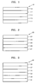
- FIG. 1 is a schematic view of an organic light emitting diode according to an embodiment of the present invention
- FIG. 2 is a schematic view of an organic light emitting diode according to another embodiment of the present invention.
- FIG. 3 is a schematic view of an organic light emitting diode according to another embodiment of the present invention.
- FIG. 1 is a schematic view of an organic light emitting diode (OLED) 10 according to an embodiment of the present invention.
- the OLED 10 includes a substrate 11, a first electrode 13, an organic layer 15, a second electrode 17, and a light-efficiency-improvement layer 18, which are sequentially formed in this order.
- the second electrode 17 may be a transmission-type electrode, and light generated in the organic layer 15 is emitted outside the organic light emitting diode 10 through the second electrode 17 and the light-efficiency-improvement layer 18.
- the substrate 11 may be any substrate that is used in a conventional organic light emitting diode.
- the substrate 11 may be a glass or transparent plastic substrate that has mechanical strength, thermal stability, a flat surface, convenience for handling, is transparent, and is waterproof.
- the first electrode 13 may be formed by depositing or sputtering a first electrode forming material on the substrate 11.
- the first electrode 13 has a first surface contacting the organic layer 15 and a second surface opposite the organic layer 15.
- the first electrode forming material may be selected from materials having a high work function so that holes are easily injected.
- the first electrode 13 may be a reflection-type electrode or a transmission-type electrode.
- the first electrode forming material may be a transparent, conductive material, such as indium tin oxide (ITO), indium zinc oxide (IZO), tin oxide (SnO 2 ), or zinc oxide (ZnO).
- the first electrode forming material may be magnesium (Mg), aluminum (Al), aluminum-lithium (Al-Li), calcium (Ca, magnesium-indium (Mg-In), or magnesium-silver (Mg-Ag).
- the organic layer 15 may be disposed on the first electrode 13.
- the term "organic layer” refers to a layer interposed between the first electrode 13 and the second electrode 17, and the organic layer may include materials other than purely organic materials.
- the organic layer can also include a metal complex.
- the organic layer 15 may include at least one layer selected from the group consisting of a hole injection layer (HIL), a hole transport layer (HTL), an emission layer (EML), a hole blocking layer (HBL), an electron transport layer (ETL), and an electron injection layer (EIL).
- HIL hole injection layer
- HTL hole transport layer
- EML emission layer
- HBL hole blocking layer
- ETL electron transport layer
- EIL electron injection layer
- An HIL may be formed on the first electrode 13 using any known method, such as a vacuum-deposition method, a spin-coating method, a casting method, or a Langmuir-Blodgett (LB) deposition method.
- a vacuum-deposition method such as a spin-coating method, a casting method, or a Langmuir-Blodgett (LB) deposition method.
- LB Langmuir-Blodgett
- deposition conditions may differ according to an HIL forming material, the target layer structure, and thermal characteristics.
- the deposition temperature may be 100 to 500°C
- the vacuum deposition pressure may be 10 -8 to 10 -3 torr (wherein 1 torr ⁇ 133 Pa)
- coating conditions may differ according to the HIL forming material, the target layer structure, and thermal characteristics.
- the coating rate may be about 2000 rpm to about 5000 rpm
- the heat treatment temperature at which solvent is removed after coating may be about 80°C to about 200°C.
- the HIL forming material may be any known hole injectable material.
- the hole injectable material include: a phthalocyanine compound such as copper phthalocyanine; 4,4',4"-tris (3-methylphenylphenylamino) triphenylamine (m-MTDATA) illustrated below; N,N'-di(1-naphthyl)-N,N'-diphenylbenzidine (NPB); TDATA illustrated below; 2T-NATA illustrated below; polyaniline/dodecylbenzenesulfonic acid (Pani/DBSA); poly(3,4-ethylenedioxythiophene)/poly(4-styrenesulfonate) (PEDOT/PSS); polyaniline/camphor sulfonic acid (Pani/CSA); and (polyaniline)/poly(4-styrenesulfonate) (PANI/PSS).
- the HIL forming material is not limited to these materials.
- the thickness of the HIL is about 100 ⁇ to about 10000 ⁇ . In another embodiment, the thickness is 100 ⁇ to 1000 ⁇ . If the thickness of the HIL is within this range, appropriate hole injection characteristics may be obtained without a substantial increase in the driving voltage. Although it is preferred to operate within this range, it may be possible to operate outside this range without departing from the scope of the present invention.
- an HTL may be formed on the HIL using any known method, such as a vacuum-deposition method, a spin-coating method, a casting method, or an LB deposition method.
- a vacuum-deposition method such as a vacuum-deposition method, a spin-coating method, a casting method, or an LB deposition method.
- deposition conditions and coating conditions may differ according to an HTL forming material.
- deposition conditions and coating conditions may be the same or similar to those described with reference to the HIL.
- the HTL forming material may be any known hole transportable material.
- the hole transportable material include: a carbazole derivative such as N-phenylcarbazole or polyvinylcarbazole; an amine derivative having an aromatic condensation ring, such as N,N'-bis(3-methylphenyl)-N,N'-diphenyl-[1,1-biphenyl]-4,4'-diamine (TPD) illustrated below or N,N'-di(naphthalene-1-yl)-N,N'-diphenyl benzidine ( ⁇ -NPD) illustrated below ; and a triphenylamine-based material, such as 4,4',4"-tris(N-carbazolyl)triphenylamine(4,4',4"-tris(N-carbazolyl)triphenylamine) (TCTA).
- TCTA may have, in addition to a hole transporting capability, a capability of blocking diffusion of excitons generated in the EML.
- the thickness of the HTL is about 50 ⁇ to about 1000 ⁇ . In another embodiment, the thickness may be 100 ⁇ to 800 ⁇ . If the thickness of the HTL is within this range, appropriate hole transporting characteristics can be obtained without a substantial increase in the driving voltage. Although it is preferred to operate within this range, it may be possible to operate outside this range without departing from the scope of the present invention.
- an EML may be formed on the HTL using any known method, such as a vacuum-deposition method, a spin-coating method, a casting method, or an LB deposition method.
- a vacuum-deposition method such as a vacuum-deposition method, a spin-coating method, a casting method, or an LB deposition method.
- deposition conditions and coating conditions may differ according to an EML forming material.
- deposition conditions and coating conditions may be the same or similar to those described with reference to the HIL.
- the EML may include a compound or a combination of a host and a dopant.
- Examples of the host include Alq 3 , 4,4'-N,N'-dicarbazole-biphenyl (CBP), poly(n-vinylcarbazole) (PVK) illustrated below, 9,10-di(naphthalene-2-yl)anthracene (ADN) illustrated below, TCTA, 1,3,5-tris(N-phenylbenzimidazole-2-yl)benzene(1,3,5-tris(N-phenylbenzimidazole-2-yl)benzene) (TPBI) illustrated below, 3-tert-butyl-9,10-di(naphth-2-yl) anthracene (TBADN) illustrated below, E3 illustrated below, and distyrylarylene (DSA).
- CBP 4,4'-N,N'-dicarbazole-biphenyl
- PVK poly(n-vinylcarbazole)
- ADN 9,10-di(naphthalene-2-y
- red dopant examples include PtOEP, Ir(piq) 3 , Btp 2 Ir(acac), which are illustrated below, and DCJTB.
- the red dopant is not limited to these materials.
- the green dopant is not limited to these materials.
- Examples of a known blue dopant include F 2 Irpic illustrated below, (F 2 ppy) 2 Ir(tmd) illustrated below, Ir(dfppz) 3 illustrated below, ter-fluorene, 4,4'-bis[4-(dip-tolylamino)styryl] biphenyl (DPAVBi) illustrated below, and 2,5,8,11-tetra- tert -butyl perylene (TBPe) illustrated below.
- the blue dopant is not limited to these materials.
- the doping concentration of the dopant is not limited.
- the content of the dopant may be 0.01 to 15 parts by weight based on 100 parts by weight of the host.
- the thickness of the EML is about 100 ⁇ to about 1000 ⁇ . In another embodiment, the thickness is 200 ⁇ to 600 ⁇ . If the thickness of the EML is within this range, excellent luminescent characteristics can be obtained without a substantial increase in the driving voltage. Although it is preferred to operate within this range, it may be possible to operate outside this range without departing from the scope of the present invention.
- the EML When the EML is formed using a phosphorescent dopant, diffusion of triplet excitons or holes into the ETL can be prevented by forming an HBL between the ETL and the EML using any method selected from a vacuum-deposition method, a spin-coating method, a casting method, and an LB deposition method.
- deposition conditions and coating conditions may differ according to an HBL forming material.
- deposition conditions and coating conditions may be the same or similar to those described with reference to the HIL.
- the HBL forming material may be any known hole blocking material.
- examples of the hole blocking material include an oxadiazole derivative, a triazole derivative, and a phenanthroline derivative.
- the thickness of the HBL is about 50 ⁇ to about 1000 ⁇ . In another embodiment, the thickness is 100 ⁇ to 300 ⁇ . If the thickness of the HBL is within this range, excellent hole blocking characteristics can be obtained without a substantial increase in the driving voltage. Although it is preferred to operate within this range, it may be possible to operate outside this range without departing from the scope of the present invention.
- an ETL may be formed using any known method, such as a vacuum-deposition method, a spin-coating method, or a casting method.
- deposition conditions and coating conditions may differ according to an ETL forming material.
- deposition conditions and coating conditions may be the same or similar to those described with reference to the HIL.
- the ETL forming material may be any known electron transporting material that stably transports electrons injected from an electron injection electrode, that is, a cathode.
- the electron transporting material include quinoline derivatives, such as tris(8-quinolinolate)aluminum (Alq 3 ), TAZ illustrated below, and BAlq illustrated below.
- the ETL forming material is not limited to these materials.
- the thickness of the ETL is about 100 ⁇ to about 1000 ⁇ . In another embodiment, the thickness is 150 ⁇ to 500 ⁇ . If the thickness of the ETL is within this range, appropriate electron transporting characteristics can be obtained without a substantial increase in the driving voltage. Although it is preferred to operate within this range, it may be possible to operate outside this range without departing from the scope of the present invention.
- an EIL may be formed by depositing an EIL forming material on the ETL.
- the EIL forming material may be a material that allows electrons to be easily injected.
- the EIL forming material is not limited, and may be any known EIL forming material, such as LiF, NaCl, CsF, Li 2 O, or BaO.
- Deposition conditions of the EIL may differ according to the EIL forming material. In general, deposition conditions may be the same or similar to those described with reference to the HIL.
- the thickness of the EIL may be about 1 ⁇ to about 100 ⁇ . In another embodiment, the thickness may be 5 ⁇ to 90 ⁇ . If the thickness of the EIL is within this range, appropriate electron injection characteristics can be obtained without a substantial increase in the driving voltage. Although it is preferred to operate within this range, it may be possible to operate outside this range without departing from the scope of the present invention.
- the second electrode 17 that is a transmission-type electrode may be disposed on the organic layer 15.
- the second electrode 17 has a first surface contacting with the organic layer 15 and a second surface being opposite to the organic layer 15.
- the second electrode 17 may be a cathode that is an electron injection electrode.
- a second electrode forming metal may be a metal having a low work function, an alloy having a low work function, an electro-conductive compound, or mixtures thereof.
- examples of the second electrode forming metal include lithium (Li), magnesium (Mg), aluminum (Al), aluminum-lithium (Al-Li), calcium (Ca), magnesium-indium (Mg-In), and magnesium-silver (Mg-Ag).
- the second electrode 17 may be a transmission-type electrode formed of ITO or IZO.
- the light-efficiency-improvement layer 18 is disposed on the second surface of the second electrode 17.
- the light-efficiency-improvement layer 18 contains a compound represented by Formula 1: where Ar may be a substituted or unsubstituted C 5 -C 30 aromatic ring system or a substituted or unsubstituted C 2 -C 30 hetero aromatic ring system.
- Ar examples include substituted or unsubstituted pentalenes, substituted or unsubstituted indenes, substituted or unsubstituted naphthalenes, substituted or unsubstituted azulenes, substituted or unsubstituted heptalenes, substituted or unsubstituted indacenes, substituted or unsubstituted acenaphthylenes, substituted or unsubstituted fluorenes, substituted or unsubstituted phenalenes, substituted or unsubstituted phenanthrenes, substituted or unsubstituted anthracenes, substituted or unsubstituted fluoranthenes, substituted or unsubstituted triphenylenes, substituted or unsubstituted pyrenes, substituted or unsubstituted chrysenes, substituted or unsubstituted naphthacenes, substituted or unsubsti
- Ar may be, as described above, in addition to the unsubstituted C 5 -C 30 aromatic ring system or the unsubstituted C 2 -C 30 hetero aromatic ring system, the substituted C 5 -C 30 aromatic ring system or the substituted C 2 -C 30 hetero aromatic ring system.
- a substituent may be substituted or unsubstituted C 6 -C 14 aryl groups or substituted or unsubstituted C 2 -C 14 hetero aryl groups.
- the substituent may be a phenyl group, a halophenyl group, a C 1 -C 10 alkylphenyl group, a C 1 -C 10 alkoxyphenyl group, a naphthyl group, a halonaphthyl group, a C 1 -C 10 alkylnaphthyl group, a C 1 -C 10 alkoxynaphthyl group, a pyridinyl group, a halopyridinyl group, a C 1 -C 10 alkylpyridinyl group, a C 1 -C 10 alkoxypyridinyl group, a quinolinyl group, a haloquinolinyl group, a C 1 -C 10 alkylquinolinyl group, a C 1 -C 10 alkoxyquinolinyl group, an isoquinolinyl group, a haloisoquinoliny
- L 1 may be a substituted or unsubstituted C 1 -C 30 alkylene group, a substituted or unsubstituted C 5 -C 30 arylene group, or a substituted or unsubstituted C 2 -C 30 hetero arylene group.
- L 1 may be a substituted or unsubstituted C 6 -C 14 arylene group or a substituted or unsubstituted C 2 -C 14 hetero arylene group.
- L 1 may be a phenylene group, a halophenylene group, a C 1 -C 10 alkylphenylene group, a C 1 -C 10 alkoxyphenylene group, a naphthylene group, a halonaphthylene group, a C 1 -C 10 alkylnaphthylene group, or a C 1 -C 10 alkoxynaphthylene group, but is not limited thereto.
- a denotes a repeat number of L 1 , and may be an integer of 0 to 10. If a is 0, in Formula 1, a cyclic or heterocyclic ring situated at the right side of L 1 may be directly connected to Ar. If a is 2 or greater, a plurality of L 1 may be identical to or different from each other. In a preferred embodiment, a is from 0 to 3, in a particularly preferred embodiment, a is 0, and in another particularly preferred embodiment, a is 1.
- -(L 1 ) a - may be represented by any one of Formulae 2A through 2G, but is not limited thereto:
- * represents a binding site with Ar
- *' represents a binding site with the heterocycle at the right side of L 1 in Formula 1.
- -(L 1 ) a - is represented by Formula 2a.
- X 1 is N, CY 1 , or a binding site with L 1 or Ar
- X 2 is N, CY 2 , or a binding site with L 1 or Ar
- X 3 is N, CY 3 , or a binding site with L 1 or Ar
- X 4 is N, CY 4 , or a binding site with L 1 or Ar
- X 5 is N, CY 5 , or a binding site with L 1 or Ar
- X 6 is N, CY 6 , or a binding site with L 1 or Ar, wherein any one of X 1 through X 6 is a binding site with L 1 or Ar.
- X 1 is X 1 is N, CY 1 , or a carbon atom bonded to L 1 or Ar;
- X 2 is N, CY 2 , or a carbon atom bonded to L 1 or Ar;
- X 3 is N, CY 3 , or a carbon atom bonded to L 1 or Ar;
- X 4 is N;
- X 5 is a carbon atom;
- X 6 is N or CY 6 ; wherein one of X 1 , X 2 and X 3 is a carbon atom bonded to L 1 or Ar.
- X 1 is preferably CY 1 or N;
- X 2 is preferably a carbon atom bonded to L 1 or Ar;
- X 3 is preferably CY 3 or N;
- X 4 is preferably N;
- X 5 is preferably a carbon atom;
- X 6 is preferably N or CY 6 .
- At least one of X 1 , X 4 and X 6 is N. In certain embodiments, each of X 1 and X 4 is N. In certain other embodiments, each of X 1 , X 4 and X 6 is N.
- each of R 1 through R 3 , and Y 1 through Y 6 in X 1 through X 6 is independently a hydrogen atom, a halogen atom, a hydroxyl group, a cyano group, a substituted or unsubstituted C 1 -C 30 alkyl group, a substituted or unsubstituted C 1 -C 30 alkoxy group, a substituted or unsubstituted C 1 -C 30 acyl group, a substituted or unsubstituted C 2 -C 30 alkenyl group, a substituted or unsubstituted C 2 -C 30 alkynyl group, a substituted or unsubstituted C 5 -C 30 aryl group, or a substituted or unsubstituted C 2 -C 30 hetero aryl group.
- two or more neighboring substituents selected from R 1 through R 3 and Y 1 through Y 6 may be selectively bonded to each other to form
- each of R 1 through R 3 and Y 1 through Y 6 is independently a hydrogen atom, a substituted or unsubstituted C 1 -C 10 alkyl group, a substituted or unsubstituted C 2 -C 10 alkenyl group, a substituted or unsubstituted C 6 -C 14 aryl group, or a C 2 -C 14 hetero aryl group.
- each of R 1 through R 3 and Y 1 through Y 6 is independently selected from a hydrogen atom, C 1 -C 10 alkyl groups, C 1 -C 10 halo alkyl groups, C 2 -C 10 alkenyl groups, C 2 -C 10 halo alkenyl groups, phenyl groups, halophenyl groups, C 1 -C 10 alkylphenyl groups, C 1 -C 10 alkoxyphenyl groups, naphthyl groups, halonaphthyl groups, C 1 -C 10 alkylnaphthyl groups, or C 1 -C 10 alkoxynaphthyl groups, but is not limited thereto.
- each of R 1 , through R 3 and Y 1 through through Y 6 is independently selected from a hydrogen atom, a methyl group and a phenyl group.
- Y 3 , Y 6 , R 1 , R 2 and R 3 are a hydrogen atom.
- R 3 is selected from a hydrogen atom, a methyl group and a phenyl group.
- Y 6 and R 1 are bonded to each other to form a saturated or unsaturated ring, preferably a phenyl ring.
- m denotes the number of the heterocyclic ring situated at the right side of L 1 , wherein the heterocyclic ring can be bonded to L 1 or Ar and m is dependent upon the structure of Ar or L 1 .
- m may be an integer from 1 to 5.
- m is 1.
- m is 2.
- n is an integer from 1 to 10, and is dependent upon the structure of Ar. In a preferred embodiment, n is 1.
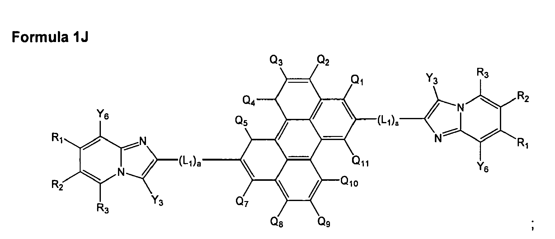
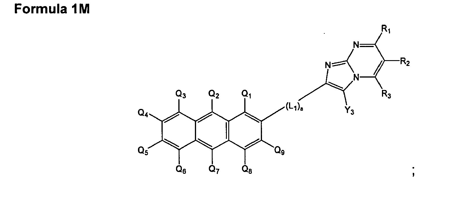
- the compound represented by Formula 1 may be any one compound selected from compounds represented by Formulae 1A through 1X, but is not limited thereto:
- each of Q 1 through Q 11 may be independently a hydrogen atom, a substituted or unsubstituted C 6 -C 14 aryl group, or a substituted or unsubstituted C 2 -C 14 hetero aryl group.
- each of Q 1 through Q 11 is independently selected from a hydrogen atom, phenyl group, a halophenyl group, a C 1 -C 10 alkylphenyl group, a C 1 -C 10 alkoxyphenyl group, a naphthyl group, a halonaphthyl group, a C 1 -C 10 alkylnaphthyl group, a C 1 -C 10 alkoxynaphthyl group, a pyridinyl group, a halopyridinyl group, a C 1 -C 10 alkylpyridinyl group, a C 1 -C 10 alkoxypyridinyl group, a quinolinyl group, a haloquinolinyl group, a C 1 -C 10 alkylquinolinyl group, a C 1 -C 10 alkoxyquinolinyl group, an isoquinolinyl group
- each of Q 2 and Q 7 is a substituted or unsubstituted C 6 -C 14 aryl group or a substituted or unsubstituted C 2 -C 14 hetero aryl group.
- each of Q 2 and Q 7 is independently selected from a phenyl group and a naphthyl group and Q 1 , Q3-Q6 and Q8-Q9 are all a hydrogen atom.
- L 1 may be a substituted or unsubstituted C 6 -C 14 arylene group, or a substituted or unsubstituted C 2 -C 14 hetero arylene group.
- L 1 may be a phenylene group, a halophenylene group, a C 1 -C 10 alkylphenylene group, a C 1 -C 10 alkoxyphenylene group, a naphthylene group, a halonaphthylene group, a C 1 -C 10 alkylnaphthylene group, or a C 1 -C 10 alkoxynaphthylene group, but is not limited thereto.
- each of R 1 , R 2 , R 3 , Y 2 , Y 3 and Y 6 may be independently a hydrogen atom, a substituted or unsubstituted C 1 -C 10 alkyl group, a substituted or unsubstituted C 2 -C 10 alkenyl group, a substituted or unsubstituted C 6 -C 14 aryl group, or a C 2 -C 14 hetero aryl group.
- two or more neighboring elements selected from R 1 , R 2 , R 3 and Y 6 may be selectively bonded to each other to form a C 6 -C 12 aromatic ring.
- a is 1 or 2, and is preferably 1.
- the compound represented by Formula 1 may be any compound selected from Compounds 1 through 64, but is not limited thereto:
- the unsubstituted C 1 -C 30 alkyl group may be methyl, ethyl, propyl, isobutyl, sec-butyl, pentyl, iso-amyl, or hexyl.
- one or more hydrogen atoms may be substituted with a halogen atom, a hydroxyl group, a nitro group, a cyano group, an amino group, an amidino group, a hydrazine, a hydrazone, a carboxylic group or salt thereof, a sulfonic acid group or salt thereof, a phosphoric acid or salt thereof, a C 1 -C 30 alkyl group, a C 1 -C 30 alkenyl group, a C 1 -C 30 alkynyl group, a C 6 -C 30 aryl group, a C 7 -C 20 aryl alkyl group, a C 2 -C 20 hetero aryl group, or a C 3 -C 30 hetero aryl alkyl group.
- the unsubstituted C 1 -C 30 alkylene group refers to a divalent group having the same structure as the unsubstituted C 1 -C 30 alkyl group described above.
- the unsubstituted C 1 -C 30 alkoxy group may be represented by -OA where A is an unsubstituted C 1 -C 30 alkyl group described above.
- suitable unsubstituted C 1 -C 30 alkoxy groups include methoxys, ethoxys, and isopropyloxys.
- one or more hydrogen atoms may be substituted with the substituents which have been described with the unsubstituted C 1 -C 30 alkyl group.
- examples of unsubstituted C 1 -C 30 acyl groups include acetyls, ethylcarbonyls, isopropylcarbonyls, phenylcarbonyls, naphthylenecarbonyls, diphenylcarbonyls, and cyclohexylcarbonyls.
- one or more hydrogen atoms may be substituted with the substituents which have been described with the unsubstituted C 1 -C 30 alkyl group.
- the unsubstituted C 2 -C 30 alkenyl group refers to unsubstituted C 1 -C 30 alkyl groups which have a C-C double bond in the center or end thereof.
- suitable unsubstituted C 2 -C 30 alkenyl group include ethenyls, propenyls, and butenyls.
- one or more hydrogen atoms may be substituted with the substituents which have been described with the unsubstituted C 1 -C 30 alkyl group.
- the unsubstituted C 2 -C 30 alkynyl group refers to unsubstituted C 1 -C 30 alkyl groups that have a C-C triple bond in the center or end thereof.
- suitable unsubstituted C 2 -C 30 alkynyl groups include acetylenes, propylenes, phenylacetylenes, naphthylacetylenes, isopropylacetylenes, t-butylacetylenes, and diphenylacetylenes.
- one or more hydrogen atoms may be substituted with the substituents which have been described with the unsubstituted C 1 -C 30 alkyl group.
- the unsubstituted C 5 -C 30 aromatic ring system refers to a carbocyclic aromatic system having one or more aromatic rings and 5-30 carbon atoms.
- the aromatic ring system includes 2 or more rings, the 2 or more rings may be fused together or connected to each other through a single bond.
- one or more hydrogen atoms may be substituted with the substituents which have been described with the unsubstituted C 1 -C 30 alkyl group.
- the unsubstituted C 2 -C 30 hetero aromatic ring system refers to an aromatic system including one or more aromatic rings that have one or more hetero atoms selected from N, O, P and S, wherein, in the one or more aromatic rings, the other ring atoms are carbon atoms (C).
- the unsubstituted C 2 -C 30 hetero aromatic ring system includes two or more rings, the two or more rings may be fused together or connected to each other through a single bond.
- one or more hydrogen atoms may be substituted with the substituents which have been described with the unsubstituted C 1 -C 30 alkyl group.
- unlimited examples of the substituted or unsubstituted C 2 -C 30 hetero aromatic ring system and unlimited examples of the substituent thereof have already been described above.
- the unsubstituted C 5 -C 30 aryl group refers to a monovalent group including a carbocyclic aromatic system having one or more aromatic rings and 5-30 carbon atoms
- the unsubstituted C 5 -C 30 arylene group refers to a divalent group including a carbocyclic aromatic system having one or more aromatic rings and 5-30 carbon atoms.
- the two or more rings may be fused together or connected to each other through a single bond.
- one or more hydrogen atoms may be substituted with the substituents which have been described with the unsubstituted C 1 -C 30 alkyl group.
- substituted or unsubstituted C 5 -C 30 aryl groups include: phenyl groups; C 1 -C 10 alkylphenyl groups such as ethylphenyl groups, C 1 -C 10 alkylbiphenyl groups such as ethylbiphenyl groups, halophenyl groups such as o-, m- and p-fluorophenyl groups or dichlorophenyl groups, dicyanophenyl groups, trifluoromethoxyphenyl groups, o-, m-, and p-tolyl groups, o-, m- and p-cumenyl groups, mesityl groups, phenoxyphenyl groups, ( ⁇ , ⁇ -dimethylbenzene)phenyl groups, (N,N'-dimethyl)aminophenyl groups, (N,N'-diphenyl)aminophenyl groups, pentalenyl groups, indenyl groups, naph
- the unsubstituted C 2 -C 30 hetero aryl group refers to a monovalent group including one or more aromatic rings that has one or more hetero atoms selected from N, O, P and S, wherein, in the one or more aromatic rings, the other ring atoms are carbon atoms (C); and the unsubstituted C 2 -C 30 hetero arylene group refers to a bivalent group including one or more aromatic rings that has one or more hetero atoms selected from N, O, P and S, wherein, in the one or more aromatic rings, the other ring atoms are carbon atoms (C).
- the unsubstituted C 2 -C 30 hetero aryl group or the unsubstituted C 2 -C 30 hetero arylene group includes two or more rings, the two or more rings may be fused together or connected to each other through a single bond.
- one or more hydrogen atoms may be substituted with the substituents which have been described with the unsubstituted C 1 -C 30 alkyl group.
- Suitable unsubstituted C 2 -C 30 hetero aryl groups include pyrazolyl groups, imidazolyl groups, oxazolyl groups, thiazolyl groups, triazolyl groups, tetrazolyl groups, oxadiazolyl groups, pyridinyl groups, pyridazinyls, pyrimidinyl groups, triazinyl groups, carbazolyl groups, indolyl groups, quinolinyl groups, and isoquinolinyl groups.
- suitable substituted or unsubstituted C 2 -C 30 hetero arylene groups may be easily recognized with reference to examples of substituted or unsubstituted C 5 -C 30 arylene groups.
- the compound represented by Formula 1 may be prepared using various known methods, which would be obvious to one of ordinary skill in the art.
- the compound represented by Formula 1 can be obtained by reacting the compound represented by Formula 3 with the compound represented by Formula 4: Ar-[B(OH) 2 ] n Formula 3
- the light-efficiency-improvement layer 18 including the compound represented by Formula 1 has a high refractive index, and thus, light efficiency, specifically external luminescent efficiency, of the OLED 10 is relatively high.
- the light-efficiency-improvement layer 18 may have a refractive index of 1.8 or more, specifically 1.9 or more, at a wavelength of about 630 nm.
- an organic light emitting diode includes a plurality of layers formed of various materials. Accordingly, at least some of the light generated in an organic layer may be reflected due to total internal reflection while passing through the layers and thus, may not be emitted outside the organic light emitting diode. Where the external luminescent efficiency of the organic light emitting diode is low, even when the light conversion efficiency in the organic layer is high, the entire light efficiency of the organic light emitting diode can be relatively low. However, when light generated in the organic layer 15 is emitted outside the organic light emitting diode through the second electrode 17 and the light-efficiency-improvement layer 18, the light-efficiency-improvement layer 18 may increase the external luminescent efficiency by constructive interference.
- the light-efficiency-improvement layer 18 is disposed on a surface of the second electrode 17.
- various layers may be further disposed between the light-efficiency-improvement layer 18 and the second electrode 17.
- a sealing layer for sealing the OLED 10 may be further disposed on the light-efficiency-improvement layer 18.
- the OLED 10 according to the current embodiment may have various modifications.
- FIG. 2 is a schematic view of an OLED 20 according to another embodiment of the present invention.
- the organic light emitting diode 20 includes a substrate 21, a light-efficiency-improvement layer 28, a first electrode 23, an organic layer 25, and a second electrode 27 which are sequentially disposed in this order.
- the first electrode 23 has a first surface contacting with the organic layer 25 and a second surface being opposite to the organic layer 25.
- the light-efficiency-improvement layer 28 is formed on the second surface of the first electrode 23.
- the first electrode 23 is a transmission-type electrode, and light generated in the organic layer 25 is emitted outside the organic light emitting diode 20 through the first electrode 23 and the light-efficiency-improvement layer 28.
- the layers of the organic light emitting diode 20 are the same as the corresponding layers of the OLED 10, and thus detailed descriptions thereof will not be provided here.
- the light-efficiency-improvement layer 28 includes the compound represented by Formula 1 and thus, has a high refractive index. Accordingly, light generated in the organic layer 25 can be efficiently emitted outside the OLED 20 by constructive interference. Therefore, the light efficiency of the OLED 20 is relatively high.
- FIG. 3 is a schematic view of an OLED 30 according to another embodiment of the present invention.
- the OLED 30 according to the present embodiment includes a substrate 31, a first light-efficiency-improvement layer 38, a first electrode 33, an organic layer 35, a second electrode 37, and a second light-efficiency-improvement layer 39 which are sequentially disposed in this order.
- the first electrode 31 and the second electrode 37 are transmission-type electrodes. Accordingly, light generated in the organic layer 35 can be emitted outside the OLED 30 through the first electrode 31 and the first light-efficiency-improvement layer 38 and also through the second electrode 37 and the second light-efficiency-improvement layer 39.
- the layers of the OLED 30 are the same as the corresponding layers of the OLED 10, and thus detailed descriptions thereof will not be provided here.
- Each of the first light-efficiency-improvement layer 38 and the second light-efficiency-improvement layer 39 contain the compound represented by Formula 1 and thus, have a high refractive index. Accordingly, light generated in the organic layer 35 can be efficiently emitted outside the OLED 30 according to constructive interference. Therefore, the light efficiency of the OLED 30 is relatively high.
- an organic layer may be individually patterned corresponding to R, G and B pixels. Accordingly, the organic layer may include a red light emitting organic layer, a green light emitting organic layer, and a blue light emitting organic layer.
- a light-efficiency-improvement layer including the compound represented by Formula 1 described above may be a common layer with respect to the R, G and B pixels.
- the thickness of the light-efficiency-improvement layer may be 500 ⁇ to 800 ⁇ . In other embodiments, the thickness may be 600 ⁇ to 700 ⁇ . If the thickness of the light-efficiency-improvement layer is within this range, the light efficiency of the organic light emitting diode may be improved. Although it is preferred to operate within this range, it may be possible to operate outside this range without departing from the scope of the present invention.
- the light-efficiency-improvement layer may include one or more layers selected from a light-efficiency-improvement layer-R, a light-efficiency-improvement layer-G, and a light-efficiency-improvement layer-B. That is, the light-efficiency-improvement layer can be individually patterned corresponding to the R, G and B pixels.
- the term "light-efficiency-improvement layer-R” refers to a light-efficiency-improvement layer formed in an area corresponding to the R pixel.
- the term "light-efficiency-improvement layer-G” refers to a light-efficiency-improvement layer formed in an area corresponding to the G pixel.
- the term "light-efficiency-improvement layer-B" refers to a light-efficiency-improvement layer formed in an area corresponding to the B pixel.
- the light-efficiency-improvement layer-R, the light-efficiency-improvement layer-G and the light-efficiency-improvement layer-B may be formed on at least one of the second surface of the first electrode and the second surface of the second electrode.
- the light-efficiency-improvement layer-R, the light-efficiency-improvement layer-G and the light-efficiency-improvement layer-B may have the same or different thicknesses.
- the resultant mixture was dissolved with ethylether, and petroleum ether was added thereto and stirred, thereby obtaining a solid compound.
- the solid compound was dried in a vacuum condition to obtain 17.6 g of dinaphthyldialcohol.
- Compound 2 was prepared in the same manner as in Synthesis Example 1, except that Intermediate 2c was used instead of Intermediate 1c, wherein Intermediate 2c was prepared using phenylmagnesiumbromide instead of 2-naphthylmagnesiumbromide that was used to obtain Intermediates 1 b and 1 c in Synthesis Example 1.
- 4.6 g (Yield: 73%) of Compound 2 that was yellow powder was obtained through a Suzuki reaction between 5 g (13.36 mmol) of Intermediate 2c and 3.32 g (12.15 mmol) of Intermediate 1d.
- Compound 3 was prepared in the same manner as in Synthesis Example 1, except that Intermediate 3d was used instead of Intermediate 1d, wherein Intermediate 3d was prepared using 2,4'-diboromopropiophenone instead of 2,4'-dibromoacetophenone that was used to prepare Intermediate 1 d. 4.15 g (Yield: 68%) of Compound 3 that was yellow powder was obtained through a Suzuki reaction between 5 g (10.54 mmol) of Intermediate 1c and 2.75 g (9.58 mmol) of Intermediate 3d.
- Compound 7 was prepared in the same manner as in Synthesis Example 1, except that Intermediate 7d was used instead of Intermediate 1d, wherein Intermediate 7d was prepared using 1-aminoisoquinoline instead of 2-aminopyridine. 9.03 g (Yield: 70%) of Compound 7 that was light yellow powder was prepared through a Suzuki reaction between 10 g (21.08 mmol) of Intermediate 1c and 6.19 g (19.16 mmol) of Intermediate 7d.
- Intermediate 1d was prepared in the same manner as in Synthesis Example 1, and then, 5 g of Intermediate 1d, 4.5 g of pyrene-1-yl-1-boronic acid, 0.46 g of tetrakis(triphenylphosphine)paladium, 6 g of potassium carbonate were dissolved in a solvent mixture including 80 ml of THF and 80 ml of water. The resultant mixture was stirred at a reflux temperature for 18 hours. The reaction product was cooled to room temperature and a first organic layer was separated. 80 ml of dichloromethane was added to an aqueous layer to extract a second organic layer.
- the first and second organic layers were put together and dried with magnesium sulfate to remove the solvent used, thereby obtaining a crude product.
- the crude product was refined by silica-gel-column chromatography to obtain 5.5 g of Compound 12.
- the resulting compound was evaluated by NMR analysis with the following results: 1H NMR (DMSO-d6, 400MHz) ⁇ (ppm) 8.56 (1H, d), 8.51 (1H, s), 8.36 (1H, d), 8.31 (1H, d), 8.28 (1H, d), 8.22 ⁇ 8.18 (6H, m), 8.10 ⁇ 8.05 (2H, m), 7.70 (2H, d), 7.61 (1H, d), 7.26 (1H, t), 6.91 (1H, t)
- Intermediate 4d was prepared in the same manner as in Synthesis Example 4, and then, 2.9 g of Intermediate 4d, 2.0 g of pyrene-1-yl-1-boronic acid, 1.03 g of tetrakis(triphenylphosphine)palladium, and 13 g of potassium carbonate were dissolved in a solvent mixture including 40 ml of THF and 40 ml of water. The resultant mixture was stirred at a reflux temperature for 18 hours. The reaction product was cooled to room temperature and a first organic layer was separated. 40 ml of dichloromethane was added to an aqueous layer to extract a second organic layer.
- the first and second organic layers were put together and were dried with magnesium sulfate to remove the solvent used, thereby obtaining a crude product.
- the crude product was refined by silica-gel-column chromatography to obtain 3.0 g of Compound 14.
- the resulting compound was evaluated by NMR analysis with the following results: 1H NMR (DMSO-d6, 400MHz) d (ppm) 8.24 ⁇ 8.13 (4H, m), 8.07 (2H, s), 8.01 ⁇ 7.97 (4H, m), 7.89 (2H, d), 7.73 (1H, d), 7.57 (7H, br s), 7.22 (1H, t), 6.74 (1H, t)
- Intermediate 7d was prepared in the same manner as in Synthesis Example 5, and then 3.94 g of Intermediate 7d, 3.0 g of pyrene-1-yl-1-boronic acid, 0.7 g of tetrakis(triphenylphosphine)palladium, and 8 g of potassium carbonate were dissolved in a solvent mixture including 70 ml of THF and 70 ml of water. The resultant mixture was stirred at a reflux temperature for 18 hours. The reaction product was cooled to room temperature and a first organic layer was separated. 70 ml of dichloromethane was added to an aqueous layer to extract a second organic layer.
- the first and second organic layers were put together and were dried with magnesium sulfate to remove the solvent used, thereby obtaining a crude product.
- the crude product was refined by silica-gel-column chromatography to obtain 3.7 g of Compound 17.
- the resulting compound was evaluated by NMR analysis with the following results: 1H NMR (DMSO-d6, 400MHz) d (ppm) 8.59 (1H, d), 8.56 (1H, s), 8.41 (1H, d), 8.40 (1H, d), 8.34 (1H, d), 8.32 (1H, d), 8.27 ⁇ 8.19 (6H, m), 8.13 ⁇ 8.10 (2H, m), 7.91 (1H, d), 7.75 (2H, d), 7.72 ⁇ 7.66 (2H, m), 7.31 (1H, d)
- Compound 38 was prepared in the same manner as in Synthesis Example 10 for preparing Compound 36, except that phenylmagnesiumbromide was used instead of 2-naphthylmagnesiumbromide used to prepare Intermediate 1 b in Synthesis Example 10 and 2,4'-dibromopropiophenone was used instead of 2,4'-dibromoacetophenone used to prepare Intermediate 36d.
- the resulting compound was evaluated by NMR analysis with the following results: 1H NMR (400MHz, CDCl3) 8.54 (1H), 8.22 (1H), 7.97 (1H), 7.93 (2H), 7.70 (1H), 7.71-7.52 (15H), 7.35 (2H), 6.92 (1H), 2.73 (3H)
- Intermediate 36d was prepared in the same manner as in Synthesis Example 10, and then 3.3 g of Intermediate 36d, 3 g of pyrene-1-yl-1-boronic acid, 0.7 g of tetrakis(triphenylphosphin)palladium, and 8 g of potassium carbonate were dissolved in a solvent mixture including 70 ml of THF and 70 ml of water. The resultant mixture was stirred at a reflux temperature for 18 hours. The reaction mixture was cooled to room temperature. Then a solid product in an organic layer was filtered and washed with a solvent mixture including water and THF, thereby obtaining 2.7 g of Compound 45.
- Compound 1 prepared according to Synthesis Example 1 was vacuum-deposited on a substrate to form a light-efficiency-improvement layer having a thickness of 600 ⁇ . Then an anode was disposed on the light-efficiency-improvement layer by forming a 15 ⁇ /cm 2 (1200 A) ITO. Then, m-MTDATA was vacuum-deposited on the anode to form an HIL having a thickness of 750 ⁇ and then ⁇ -NPD was vacuum-deposited on the HIL to form an HTL having a thickness of 150 ⁇ . An EML having a thickness of 300 ⁇ was formed on the HTL by using 97 weight% of DSA constituting a host and 3 weight% of TBPe as a dopant.
- Organic light emitting diodes were manufactured in the same manner as in Example 1, except that Compounds 2, 3, 4, 7, 11, 36, 37 and 38 were used instead of Compound 1 to form the light-efficiency-improvement layer.
- An organic light emitting diode was manufactured in the same manner as in Example 1, except that Alq3 was used instead of Compound 1 to form the light-efficiency-improvement layer.
- an organic light emitting diode including a light-efficiency-improvement layer containing the compound represented by Formula 1 has excellent light efficiency.
Landscapes
- Physics & Mathematics (AREA)
- Chemical & Material Sciences (AREA)
- Engineering & Computer Science (AREA)
- Materials Engineering (AREA)
- Spectroscopy & Molecular Physics (AREA)
- Optics & Photonics (AREA)
- Organic Chemistry (AREA)
- Electroluminescent Light Sources (AREA)
- Nitrogen Condensed Heterocyclic Rings (AREA)
Abstract

Description
- The present invention relates to an organic light emitting diode including a light-efficiency-improvement layer.
- Organic light emitting diodes are self-emission devices. Organic light emitting diodes have wide viewing angles, high contrast ratios, quick response speeds, excellent luminescent characteristics, low driving voltages, and excellent colorizing characteristics.
- In general, an organic light emitting diode includes a substrate, an anode disposed on the substrate, a hole transport layer, an emission layer, an electron transport layer and a cathode, which are sequentially disposed on the anode in this order. Herein, the hole transport layer, the emission layer and the electron transport layer are organic thin films.
- An operational principle of the organic light emitting diode will now be described in detail.
- When voltage is applied between the anode and the cathode, holes injected from the anode move to the emission layer through the hole transport layer and electrons injected from the cathode move to the emission layer through the electron transport layer. The holes and electrons which are charge carriers are recombined in the emission layer, thereby generating excitons. The excitons are transferred from an excited state to a ground state, thereby generating light.
- Light efficiency of organic light emitting diodes can be categorized into internal luminescent efficiency and external luminescent efficiency. Internal luminescent efficiency relates to how efficiently excitons are generated in an organic layer interposed between a first electrode and a second electrode, that is, between the anode and the cathode and light is converted, wherein the organic layer may be a hole transport layer, an emission layer, or an electron transport layer. External luminescent efficiency (hereinafter also referred to as light coupling efficiency) relates to how efficiently light generated in the organic layer is emitted outside the organic light emitting diode. Accordingly, even if the organic layer has high light conversion efficiency, that is, the internal luminescent efficiency is high, when the light coupling efficiency is low, the whole light efficiency of the organic light emitting diode may be decreased.
- The present invention provides an organic light emitting diode that has improved light efficiency.
- According to one aspect, the present invention provides an organic light emitting diode as claimed in claim 1 of the appended set of claims. Preferred features of this aspect of the invention are set out in the claims that are dependent on claim 1.
- According to an aspect of the present invention, an organic light emitting diode is provided that includes: a substrate; a first electrode disposed on the substrate; an organic layer disposed on the first electrode; a second electrode disposed on the organic layer; and a light-efficiency-improvement layer, wherein the first electrode has a first surface contacting with the organic layer and a second surface being opposite to the organic layer, the second electrode has a first surface contacting with the organic layer and a second surface being opposite to the organic layer, and the light-efficiency-improvement layer is formed on at least one of the second surface of the first electrode and the second surface of the second electrode and comprises a compound represented by Formula 1:

- The above and other features and advantages of the present invention will become more apparent by describing in detail various embodiments thereof with reference to the attached drawings in which:
-
FIG. 1 is a schematic view of an organic light emitting diode according to an embodiment of the present invention; -
FIG. 2 is a schematic view of an organic light emitting diode according to another embodiment of the present invention; and -
FIG. 3 is a schematic view of an organic light emitting diode according to another embodiment of the present invention. - The present invention will now be described more fully with reference to the accompanying drawings, in which various embodiments of the invention are shown.
-
FIG. 1 is a schematic view of an organic light emitting diode (OLED) 10 according to an embodiment of the present invention. - Referring to
FIG. 1 , the OLED 10 according to the present embodiment includes asubstrate 11, afirst electrode 13, anorganic layer 15, asecond electrode 17, and a light-efficiency-improvement layer 18, which are sequentially formed in this order. Thesecond electrode 17 may be a transmission-type electrode, and light generated in theorganic layer 15 is emitted outside the organiclight emitting diode 10 through thesecond electrode 17 and the light-efficiency-improvement layer 18. - The
substrate 11 may be any substrate that is used in a conventional organic light emitting diode. In this regard, thesubstrate 11 may be a glass or transparent plastic substrate that has mechanical strength, thermal stability, a flat surface, convenience for handling, is transparent, and is waterproof. - The
first electrode 13 may be formed by depositing or sputtering a first electrode forming material on thesubstrate 11. Thefirst electrode 13 has a first surface contacting theorganic layer 15 and a second surface opposite theorganic layer 15. When thefirst electrode 13 is an anode, the first electrode forming material may be selected from materials having a high work function so that holes are easily injected. Thefirst electrode 13 may be a reflection-type electrode or a transmission-type electrode. The first electrode forming material may be a transparent, conductive material, such as indium tin oxide (ITO), indium zinc oxide (IZO), tin oxide (SnO2), or zinc oxide (ZnO). When thefirst electrode 13 is a reflection-type electrode, the first electrode forming material may be magnesium (Mg), aluminum (Al), aluminum-lithium (Al-Li), calcium (Ca, magnesium-indium (Mg-In), or magnesium-silver (Mg-Ag). - The
organic layer 15 may be disposed on thefirst electrode 13. In the current specification, the term "organic layer" refers to a layer interposed between thefirst electrode 13 and thesecond electrode 17, and the organic layer may include materials other than purely organic materials. In this regard, the organic layer can also include a metal complex. - The
organic layer 15 may include at least one layer selected from the group consisting of a hole injection layer (HIL), a hole transport layer (HTL), an emission layer (EML), a hole blocking layer (HBL), an electron transport layer (ETL), and an electron injection layer (EIL). - An HIL may be formed on the
first electrode 13 using any known method, such as a vacuum-deposition method, a spin-coating method, a casting method, or a Langmuir-Blodgett (LB) deposition method. - If the HIL is formed using the vacuum-deposition method, deposition conditions may differ according to an HIL forming material, the target layer structure, and thermal characteristics. In this regard, in general, the deposition temperature may be 100 to 500°C, the vacuum deposition pressure may be 10-8 to 10-3 torr (wherein 1 torr ≈ 133 Pa), and the deposition rate may be 0.01 to 100 Å/sec (wherein 1 Å = 10 -10 m).
- If the HIL is formed using the spin-coating method, coating conditions may differ according to the HIL forming material, the target layer structure, and thermal characteristics. In this regard, in general, the coating rate may be about 2000 rpm to about 5000 rpm, and the heat treatment temperature at which solvent is removed after coating may be about 80°C to about 200°C.
- The HIL forming material may be any known hole injectable material. Examples of the hole injectable material include: a phthalocyanine compound such as copper phthalocyanine; 4,4',4"-tris (3-methylphenylphenylamino) triphenylamine (m-MTDATA) illustrated below; N,N'-di(1-naphthyl)-N,N'-diphenylbenzidine (NPB); TDATA illustrated below; 2T-NATA illustrated below; polyaniline/dodecylbenzenesulfonic acid (Pani/DBSA); poly(3,4-ethylenedioxythiophene)/poly(4-styrenesulfonate) (PEDOT/PSS); polyaniline/camphor sulfonic acid (Pani/CSA); and (polyaniline)/poly(4-styrenesulfonate) (PANI/PSS). However, the HIL forming material is not limited to these materials.


- In an embodiment, the thickness of the HIL is about 100 Å to about 10000 Å. In another embodiment, the thickness is 100 Å to 1000 Å. If the thickness of the HIL is within this range, appropriate hole injection characteristics may be obtained without a substantial increase in the driving voltage. Although it is preferred to operate within this range, it may be possible to operate outside this range without departing from the scope of the present invention.
- Then an HTL may be formed on the HIL using any known method, such as a vacuum-deposition method, a spin-coating method, a casting method, or an LB deposition method. When the HTL is formed using the vacuum-deposition method or the spin-coating method, deposition conditions and coating conditions may differ according to an HTL forming material. In this regard, deposition conditions and coating conditions may be the same or similar to those described with reference to the HIL.
- The HTL forming material may be any known hole transportable material. Examples of the hole transportable material include: a carbazole derivative such as N-phenylcarbazole or polyvinylcarbazole; an amine derivative having an aromatic condensation ring, such as N,N'-bis(3-methylphenyl)-N,N'-diphenyl-[1,1-biphenyl]-4,4'-diamine (TPD) illustrated below or N,N'-di(naphthalene-1-yl)-N,N'-diphenyl benzidine (α-NPD) illustrated below ; and a triphenylamine-based material, such as 4,4',4"-tris(N-carbazolyl)triphenylamine(4,4',4"-tris(N-carbazolyl)triphenylamine) (TCTA). Specifically, TCTA may have, in addition to a hole transporting capability, a capability of blocking diffusion of excitons generated in the EML.

- In an embodiment, the thickness of the HTL is about 50 Å to about 1000 Å. In another embodiment, the thickness may be 100 Å to 800 Å. If the thickness of the HTL is within this range, appropriate hole transporting characteristics can be obtained without a substantial increase in the driving voltage. Although it is preferred to operate within this range, it may be possible to operate outside this range without departing from the scope of the present invention.
- Then an EML may be formed on the HTL using any known method, such as a vacuum-deposition method, a spin-coating method, a casting method, or an LB deposition method. When the EML is formed using the vacuum-deposition method or the spin-coating method, deposition conditions and coating conditions may differ according to an EML forming material. In this regard, deposition conditions and coating conditions may be the same or similar to those described with reference to the HIL.
- The EML may include a compound or a combination of a host and a dopant.
- Examples of the host include Alq3, 4,4'-N,N'-dicarbazole-biphenyl (CBP), poly(n-vinylcarbazole) (PVK) illustrated below, 9,10-di(naphthalene-2-yl)anthracene (ADN) illustrated below, TCTA, 1,3,5-tris(N-phenylbenzimidazole-2-yl)benzene(1,3,5-tris(N-phenylbenzimidazole-2-yl)benzene) (TPBI) illustrated below, 3-tert-butyl-9,10-di(naphth-2-yl) anthracene (TBADN) illustrated below, E3 illustrated below, and distyrylarylene (DSA). However, the host is not limited to these materials.


- Meanwhile, examples of a known red dopant include PtOEP, Ir(piq)3, Btp2Ir(acac), which are illustrated below, and DCJTB. However, the red dopant is not limited to these materials.

- Examples of a known green dopant include Ir(ppy)3 where ppy = phenylpyridine, Ir(ppy)2(acac), Ir(mpyp)3 which are illustrated below, and C545T. However, the green dopant is not limited to these materials.

- Examples of a known blue dopant include F2Irpic illustrated below, (F2ppy)2Ir(tmd) illustrated below, Ir(dfppz)3 illustrated below, ter-fluorene, 4,4'-bis[4-(dip-tolylamino)styryl] biphenyl (DPAVBi) illustrated below, and 2,5,8,11-tetra-tert-butyl perylene (TBPe) illustrated below. However, the blue dopant is not limited to these materials.


- When the dopant and the host are used together, the doping concentration of the dopant is not limited. In this regard, the content of the dopant may be 0.01 to 15 parts by weight based on 100 parts by weight of the host.
- In an embodiment, the thickness of the EML is about 100 Å to about 1000 Å. In another embodiment, the thickness is 200 Å to 600 Å. If the thickness of the EML is within this range, excellent luminescent characteristics can be obtained without a substantial increase in the driving voltage. Although it is preferred to operate within this range, it may be possible to operate outside this range without departing from the scope of the present invention.
- When the EML is formed using a phosphorescent dopant, diffusion of triplet excitons or holes into the ETL can be prevented by forming an HBL between the ETL and the EML using any method selected from a vacuum-deposition method, a spin-coating method, a casting method, and an LB deposition method. When the HBL is formed using the vacuum-deposition method or the spin-coating method, deposition conditions and coating conditions may differ according to an HBL forming material. In this regard, deposition conditions and coating conditions may be the same or similar to those described with reference to the HIL. The HBL forming material may be any known hole blocking material. In this regard, examples of the hole blocking material include an oxadiazole derivative, a triazole derivative, and a phenanthroline derivative.
- In an embodiment, the thickness of the HBL is about 50 Å to about 1000 Å. In another embodiment, the thickness is 100 Å to 300 Å. If the thickness of the HBL is within this range, excellent hole blocking characteristics can be obtained without a substantial increase in the driving voltage. Although it is preferred to operate within this range, it may be possible to operate outside this range without departing from the scope of the present invention.
- Then an ETL may be formed using any known method, such as a vacuum-deposition method, a spin-coating method, or a casting method. When the ETL is formed using the vacuum-deposition method or the spin-coating method, deposition conditions and coating conditions may differ according to an ETL forming material. In this regard, deposition conditions and coating conditions may be the same or similar to those described with reference to the HIL.
- The ETL forming material may be any known electron transporting material that stably transports electrons injected from an electron injection electrode, that is, a cathode. Examples of the electron transporting material include quinoline derivatives, such as tris(8-quinolinolate)aluminum (Alq3), TAZ illustrated below, and BAlq illustrated below. However, the ETL forming material is not limited to these materials.

- In an embodiment, the thickness of the ETL is about 100 Å to about 1000 Å. In another embodiment, the thickness is 150 Å to 500 Å. If the thickness of the ETL is within this range, appropriate electron transporting characteristics can be obtained without a substantial increase in the driving voltage. Although it is preferred to operate within this range, it may be possible to operate outside this range without departing from the scope of the present invention.
- Then an EIL may be formed by depositing an EIL forming material on the ETL. The EIL forming material may be a material that allows electrons to be easily injected. The EIL forming material is not limited, and may be any known EIL forming material, such as LiF, NaCl, CsF, Li2O, or BaO. Deposition conditions of the EIL may differ according to the EIL forming material. In general, deposition conditions may be the same or similar to those described with reference to the HIL.
- The thickness of the EIL may be about 1 Å to about 100 Å. In another embodiment, the thickness may be 5 Å to 90 Å. If the thickness of the EIL is within this range, appropriate electron injection characteristics can be obtained without a substantial increase in the driving voltage. Although it is preferred to operate within this range, it may be possible to operate outside this range without departing from the scope of the present invention.
- The
second electrode 17 that is a transmission-type electrode may be disposed on theorganic layer 15. Thesecond electrode 17 has a first surface contacting with theorganic layer 15 and a second surface being opposite to theorganic layer 15. Thesecond electrode 17 may be a cathode that is an electron injection electrode. A second electrode forming metal may be a metal having a low work function, an alloy having a low work function, an electro-conductive compound, or mixtures thereof. Specifically, examples of the second electrode forming metal include lithium (Li), magnesium (Mg), aluminum (Al), aluminum-lithium (Al-Li), calcium (Ca), magnesium-indium (Mg-In), and magnesium-silver (Mg-Ag). Meanwhile, if theOLED 10 according to the current embodiment is a front emission type device, thesecond electrode 17 may be a transmission-type electrode formed of ITO or IZO. - The light-efficiency-
improvement layer 18 is disposed on the second surface of thesecond electrode 17. - The light-efficiency-
improvement layer 18 contains a compound represented by Formula 1:
- Examples of Ar include substituted or unsubstituted pentalenes, substituted or unsubstituted indenes, substituted or unsubstituted naphthalenes, substituted or unsubstituted azulenes, substituted or unsubstituted heptalenes, substituted or unsubstituted indacenes, substituted or unsubstituted acenaphthylenes, substituted or unsubstituted fluorenes, substituted or unsubstituted phenalenes, substituted or unsubstituted phenanthrenes, substituted or unsubstituted anthracenes, substituted or unsubstituted fluoranthenes, substituted or unsubstituted triphenylenes, substituted or unsubstituted pyrenes, substituted or unsubstituted chrysenes, substituted or unsubstituted naphthacenes, substituted or unsubstituted picenes, substituted or unsubstituted perylenes, substituted or unsubstituted pentaphenes, substituted or unsubstituted hexacenes, substituted or unsubstituted pyrroles, substituted or unsubstituted pyrazoles, substituted or unsubstituted imidazoles, substituted or unsubstituted imidazolines, substituted or unsubstituted pyridines, substituted or unsubstituted pyrazines, substituted or unsubstituted pyrimidines, substituted or unsubstituted indoles, substituted or unsubstituted purines, substituted or unsubstituted quinolines, substituted or unsubstituted phthalazines, substituted or unsubstituted indolizines, substituted or unsubstituted naphthyridines, substituted or unsubstituted quinazolines, substituted or unsubstituted cinnolines, substituted or unsubstituted indazoles, substituted or unsubstituted carbazoles, substituted or unsubstituted phenazines, substituted or unsubstituted phenanthridines, substituted or unsubstituted pyrans, substituted or unsubstituted chromenes, substituted or unsubstituted benzofurans, substituted or unsubstituted thiophenes, substituted or unsubstituted benzothiophenes, substituted or unsubstituted isothiazoles, or substituted or unsubstituted isoxazoles.
- In certain embodiments, Ar may be, as described above, in addition to the unsubstituted C5-C30 aromatic ring system or the unsubstituted C2-C30 hetero aromatic ring system, the substituted C5-C30 aromatic ring system or the substituted C2-C30 hetero aromatic ring system. In the substituted C5-C30 aromatic ring system or the substituted C2-C30 hetero aromatic ring system, a substituent may be substituted or unsubstituted C6-C14 aryl groups or substituted or unsubstituted C2-C14 hetero aryl groups.
- In certain embodiments, the substituent may be a phenyl group, a halophenyl group, a C1-C10 alkylphenyl group, a C1-C10 alkoxyphenyl group, a naphthyl group, a halonaphthyl group, a C1-C10 alkylnaphthyl group, a C1-C10 alkoxynaphthyl group, a pyridinyl group, a halopyridinyl group, a C1-C10 alkylpyridinyl group, a C1-C10 alkoxypyridinyl group, a quinolinyl group, a haloquinolinyl group, a C1-C10 alkylquinolinyl group, a C1-C10 alkoxyquinolinyl group, an isoquinolinyl group, a haloisoquinolinyl group, a C1-C10 alkylisoquinolinyl group, or a C1-C10 alkoxyisoquinolinyl group, but is not limited thereto.
- In Formula 1, L1 may be a substituted or unsubstituted C1-C30 alkylene group, a substituted or unsubstituted C5-C30 arylene group, or a substituted or unsubstituted C2-C30 hetero arylene group.
- In certain embodiments, L1 may be a substituted or unsubstituted C6-C14 arylene group or a substituted or unsubstituted C2-C14 hetero arylene group. In certain embodiments, L1 may be a phenylene group, a halophenylene group, a C1-C10 alkylphenylene group, a C1-C10 alkoxyphenylene group, a naphthylene group, a halonaphthylene group, a C1-C10 alkylnaphthylene group, or a C1-C10 alkoxynaphthylene group, but is not limited thereto.
- In Formula 1, a denotes a repeat number of L1, and may be an integer of 0 to 10. If a is 0, in Formula 1, a cyclic or heterocyclic ring situated at the right side of L1 may be directly connected to Ar. If a is 2 or greater, a plurality of L1 may be identical to or different from each other. In a preferred embodiment, a is from 0 to 3, in a particularly preferred embodiment, a is 0, and in another particularly preferred embodiment, a is 1.
- In Formula 1, -(L1)a- may be represented by any one of Formulae 2A through 2G, but is not limited thereto:


- In one preferred embodiment, -(L1)a- is represented by Formula 2a.
- In Formula 1, X1 is N, CY1, or a binding site with L1 or Ar, X2 is N, CY2, or a binding site with L1 or Ar, X3 is N, CY3, or a binding site with L1 or Ar, X4 is N, CY4, or a binding site with L1 or Ar, X5 is N, CY5, or a binding site with L1 or Ar, and X6 is N, CY6, or a binding site with L1 or Ar, wherein any one of X1 through X6 is a binding site with L1 or Ar. In a preferred embodiment X1 is X1 is N, CY1, or a carbon atom bonded to L1 or Ar; X2 is N, CY2, or a carbon atom bonded to L1 or Ar; X3 is N, CY3, or a carbon atom bonded to L1 or Ar; X4 is N; X5 is a carbon atom; X6 is N or CY6; wherein one of X1, X2 and X3 is a carbon atom bonded to L1 or Ar.
- X1 is preferably CY1 or N; X2 is preferably a carbon atom bonded to L1 or Ar; X3 is preferably CY3 or N; X4 is preferably N; X5 is preferably a carbon atom; X6 is preferably N or CY6.
- In certain embodiments, at least one of X1, X4 and X6 is N. In certain embodiments, each of X1 and X4 is N. In certain other embodiments, each of X1, X4 and X6 is N.
- In Formula 1, each of R1 through R3, and Y1 through Y6 in X1 through X6 is independently a hydrogen atom, a halogen atom, a hydroxyl group, a cyano group, a substituted or unsubstituted C1-C30 alkyl group, a substituted or unsubstituted C1-C30 alkoxy group, a substituted or unsubstituted C1-C30 acyl group, a substituted or unsubstituted C2-C30 alkenyl group, a substituted or unsubstituted C2-C30 alkynyl group, a substituted or unsubstituted C5-C30 aryl group, or a substituted or unsubstituted C2-C30 hetero aryl group. In this regard, two or more neighboring substituents selected from R1 through R3 and Y1 through Y6 may be selectively bonded to each other to form a saturated or an unsaturated ring.
- In certain embodiments, each of R1 through R3 and Y1 through Y6 is independently a hydrogen atom, a substituted or unsubstituted C1-C10 alkyl group, a substituted or unsubstituted C2-C10 alkenyl group, a substituted or unsubstituted C6-C14 aryl group, or a C2-C14 hetero aryl group.
- In certain embodiments, each of R1 through R3 and Y1 through Y6 is independently selected from a hydrogen atom, C1-C10 alkyl groups, C1-C10 halo alkyl groups, C2-C10 alkenyl groups, C2-C10 halo alkenyl groups, phenyl groups, halophenyl groups, C1-C10 alkylphenyl groups, C1-C10 alkoxyphenyl groups, naphthyl groups, halonaphthyl groups, C1-C10 alkylnaphthyl groups, or C1-C10 alkoxynaphthyl groups, but is not limited thereto.
- In certain preferred embodiments, each of R1, through R3 and Y1 through through Y6 is independently selected from a hydrogen atom, a methyl group and a phenyl group. In certain preferred embodiments, Y3, Y6, R1, R2 and R3 are a hydrogen atom. In certain preferred embodiments, R3 is selected from a hydrogen atom, a methyl group and a phenyl group. In certain preferred embodiments, Y6 and R1 are bonded to each other to form a saturated or unsaturated ring, preferably a phenyl ring.
- In Formula 1, m denotes the number of the heterocyclic ring situated at the right side of L1, wherein the heterocyclic ring can be bonded to L1 or Ar and m is dependent upon the structure of Ar or L1. For example, m may be an integer from 1 to 5. In a preferred embodiment, m is 1. In another preferred embodiment, m is 2.
- In Formula 1, n is an integer from 1 to 10, and is dependent upon the structure of Ar. In a preferred embodiment, n is 1.
- According to an embodiment of the present invention, the compound represented by Formula 1 may be any one compound selected from compounds represented by Formulae 1A through 1X, but is not limited thereto:






- In Formulae 1A through 1X, each of Q1 through Q11 may be independently a hydrogen atom, a substituted or unsubstituted C6-C14 aryl group, or a substituted or unsubstituted C2-C14 hetero aryl group.
- In certain embodiments, each of Q1 through Q11 is independently selected from a hydrogen atom, phenyl group, a halophenyl group, a C1-C10 alkylphenyl group, a C1-C10 alkoxyphenyl group, a naphthyl group, a halonaphthyl group, a C1-C10 alkylnaphthyl group, a C1-C10 alkoxynaphthyl group, a pyridinyl group, a halopyridinyl group, a C1-C10 alkylpyridinyl group, a C1-C10 alkoxypyridinyl group, a quinolinyl group, a haloquinolinyl group, a C1-C10 alkylquinolinyl group, a C1-C10 alkoxyquinolinyl group, an isoquinolinyl group, a haloisoquinolinyl group, a C1-C10 alkylisoquinolinyl group, or a C1-C10 alkoxyisoquinolinyl group, but is not limited thereto.
- In certain embodiments, in Formulae 1A-1 D, and 1 M-1 P, each of Q2 and Q7 is a substituted or unsubstituted C6-C14 aryl group or a substituted or unsubstituted C2-C14 hetero aryl group. In a preferred embodiment, in Formulae 1A-1D and 1M-1P, each of Q2 and Q7 is independently selected from a phenyl group and a naphthyl group and Q1, Q3-Q6 and Q8-Q9 are all a hydrogen atom.
- In Formula 1A through 1X, L1 may be a substituted or unsubstituted C6-C14 arylene group, or a substituted or unsubstituted C2-C14 hetero arylene group.
- In certain embodiments, L1 may be a phenylene group, a halophenylene group, a C1-C10 alkylphenylene group, a C1-C10 alkoxyphenylene group, a naphthylene group, a halonaphthylene group, a C1-C10 alkylnaphthylene group, or a C1-C10 alkoxynaphthylene group, but is not limited thereto.
- In Formulae 1A through 1X, each of R1, R2, R3, Y2, Y3 and Y6 may be independently a hydrogen atom, a substituted or unsubstituted C1-C10 alkyl group, a substituted or unsubstituted C2-C10 alkenyl group, a substituted or unsubstituted C6-C14 aryl group, or a C2-C14 hetero aryl group. In this regard, two or more neighboring elements selected from R1, R2, R3 and Y6 may be selectively bonded to each other to form a C6-C12 aromatic ring.
- In Formula 1A through 1X, a is 1 or 2, and is preferably 1.
- The compound represented by Formula 1 may be any compound selected from Compounds 1 through 64, but is not limited thereto:

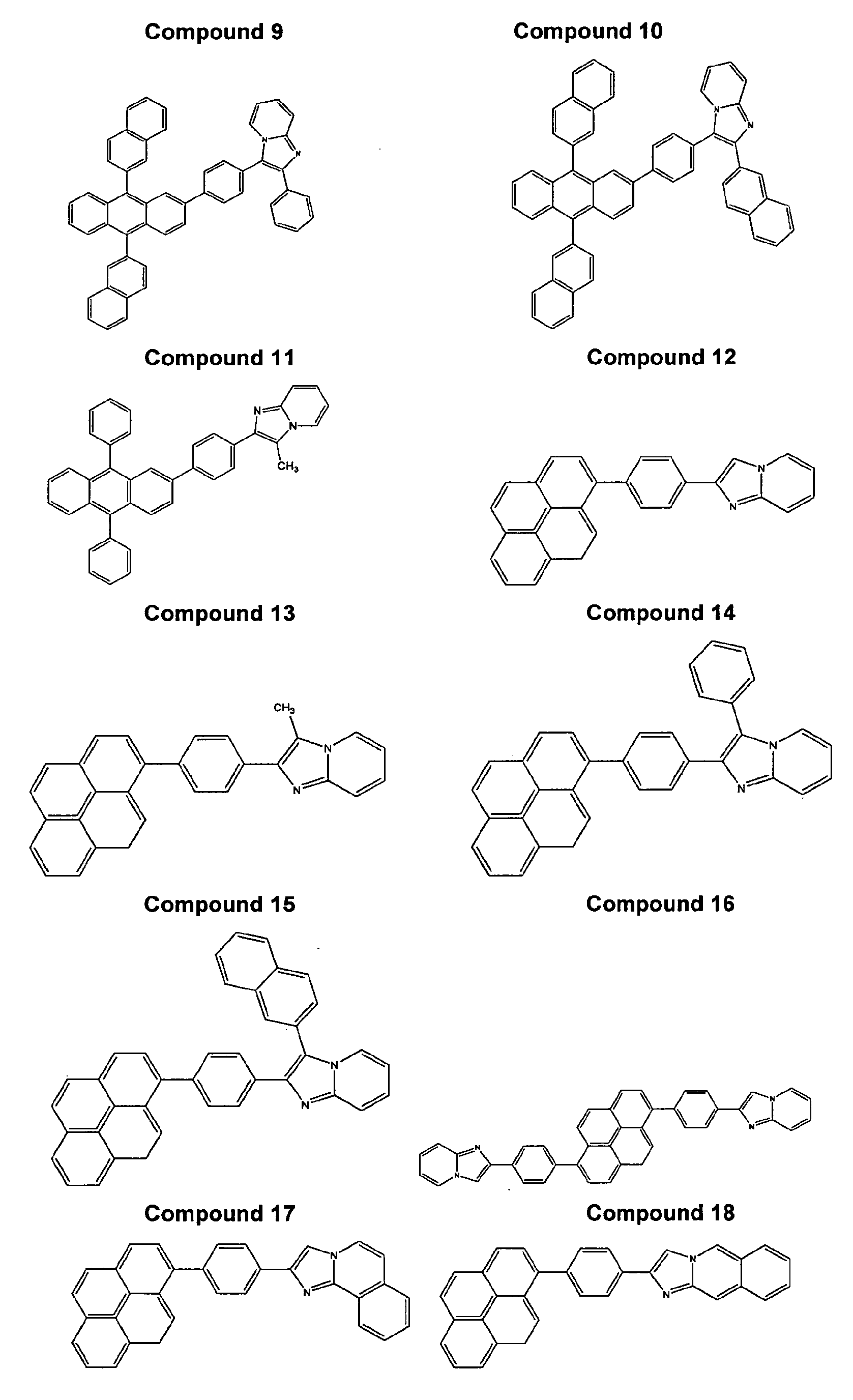


- In certain embodiments, the unsubstituted C1-C30 alkyl group may be methyl, ethyl, propyl, isobutyl, sec-butyl, pentyl, iso-amyl, or hexyl. In the unsubstituted C1-C30 alkyl group, one or more hydrogen atoms may be substituted with a halogen atom, a hydroxyl group, a nitro group, a cyano group, an amino group, an amidino group, a hydrazine, a hydrazone, a carboxylic group or salt thereof, a sulfonic acid group or salt thereof, a phosphoric acid or salt thereof, a C1-C30 alkyl group, a C1-C30 alkenyl group, a C1-C30 alkynyl group, a C6-C30 aryl group, a C7-C20 aryl alkyl group, a C2-C20 hetero aryl group, or a C3-C30 hetero aryl alkyl group.
- In certain embodiments, the unsubstituted C1-C30 alkylene group refers to a divalent group having the same structure as the unsubstituted C1-C30 alkyl group described above.
- In certain embodiments, the unsubstituted C1-C30 alkoxy group may be represented by -OA where A is an unsubstituted C1-C30 alkyl group described above. Examples of suitable unsubstituted C1-C30 alkoxy groups include methoxys, ethoxys, and isopropyloxys. In the unsubstituted C1-C30 alkoxy group, one or more hydrogen atoms may be substituted with the substituents which have been described with the unsubstituted C1-C30 alkyl group.
- In certain embodiments, examples of unsubstituted C1-C30 acyl groups include acetyls, ethylcarbonyls, isopropylcarbonyls, phenylcarbonyls, naphthylenecarbonyls, diphenylcarbonyls, and cyclohexylcarbonyls. In the unsubstituted C1-C30 acyl group, one or more hydrogen atoms may be substituted with the substituents which have been described with the unsubstituted C1-C30 alkyl group.
- In certain embodiments, the unsubstituted C2-C30 alkenyl group refers to unsubstituted C1-C30 alkyl groups which have a C-C double bond in the center or end thereof. Examples of suitable unsubstituted C2-C30 alkenyl group include ethenyls, propenyls, and butenyls. In the unsubstituted C2-C30 alkenyl group, one or more hydrogen atoms may be substituted with the substituents which have been described with the unsubstituted C1-C30 alkyl group.
- In certain embodiments, the unsubstituted C2-C30 alkynyl group refers to unsubstituted C1-C30 alkyl groups that have a C-C triple bond in the center or end thereof. Examples of suitable unsubstituted C2-C30 alkynyl groups include acetylenes, propylenes, phenylacetylenes, naphthylacetylenes, isopropylacetylenes, t-butylacetylenes, and diphenylacetylenes. In the unsubstituted C2-C30 alkynyl group, one or more hydrogen atoms may be substituted with the substituents which have been described with the unsubstituted C1-C30 alkyl group.
- In certain embodiments, the unsubstituted C5-C30 aromatic ring system refers to a carbocyclic aromatic system having one or more aromatic rings and 5-30 carbon atoms. When the aromatic ring system includes 2 or more rings, the 2 or more rings may be fused together or connected to each other through a single bond. In the unsubstituted C5-C30 aromatic ring system, one or more hydrogen atoms may be substituted with the substituents which have been described with the unsubstituted C1-C30 alkyl group. Specifically, non-limiting examples of the substituted or unsubstituted C5-C30 aromatic ring system and non-limiting examples of the substituent of the substituted or unsubstituted C5-C30 aromatic ring system have already been described above.
- In certain embodiments, the unsubstituted C2-C30 hetero aromatic ring system refers to an aromatic system including one or more aromatic rings that have one or more hetero atoms selected from N, O, P and S, wherein, in the one or more aromatic rings, the other ring atoms are carbon atoms (C). In this regard, when the unsubstituted C2-C30 hetero aromatic ring system includes two or more rings, the two or more rings may be fused together or connected to each other through a single bond. In the unsubstituted C2-C30 hetero aromatic ring system, one or more hydrogen atoms may be substituted with the substituents which have been described with the unsubstituted C1-C30 alkyl group. Specifically, unlimited examples of the substituted or unsubstituted C2-C30 hetero aromatic ring system and unlimited examples of the substituent thereof have already been described above.
- In certain embodiments, the unsubstituted C5-C30 aryl group refers to a monovalent group including a carbocyclic aromatic system having one or more aromatic rings and 5-30 carbon atoms, and the unsubstituted C5-C30 arylene group refers to a divalent group including a carbocyclic aromatic system having one or more aromatic rings and 5-30 carbon atoms. When the unsubstituted C5-C30 aryl group and the unsubstituted C5-C30 arylene group include two or more rings, the two or more rings may be fused together or connected to each other through a single bond. In each of the unsubstituted C5-C30 aryl group and the unsubstituted C5-C30 arylene group, one or more hydrogen atoms may be substituted with the substituents which have been described with the unsubstituted C1-C30 alkyl group.
- Examples of substituted or unsubstituted C5-C30 aryl groups include: phenyl groups; C1-C10 alkylphenyl groups such as ethylphenyl groups, C1-C10 alkylbiphenyl groups such as ethylbiphenyl groups, halophenyl groups such as o-, m- and p-fluorophenyl groups or dichlorophenyl groups, dicyanophenyl groups, trifluoromethoxyphenyl groups, o-, m-, and p-tolyl groups, o-, m- and p-cumenyl groups, mesityl groups, phenoxyphenyl groups, (α,α-dimethylbenzene)phenyl groups, (N,N'-dimethyl)aminophenyl groups, (N,N'-diphenyl)aminophenyl groups, pentalenyl groups, indenyl groups, naphthyl groups, halonaphthyl groups such as fluoronaphthyl groups, C1-C10 alkylnaphthyl groups such as methylnaphthyl groups, C1-C10 alkoxynaphthyl groups such as methoxynaphthyl groups, anthracenyl groups, azulenyl groups, heptarenyl groups, acenaphthylenyl groups, phenalenyl groups, fluorenyl groups, anthraquinolyl groups, methylanthryl groups, phenanthryl groups, triphenylene groups, pyrenyl groups, chrysenyl groups, ethyl-chrysenyl groups, picenyl groups, perylenyl groups, chloroperilenyl groups, pentaphenyl groups, pentacenyl groups, tetraphenylenyl groups, hexaphenyl groups, hexacenyl groups, rubicenyl groups, coroneryl groups, trinaphthylenyl groups, heptaphenyl groups, heptacenyl groups, pyranthrenyl groups, and ovalenyl groups. Examples of substituted or unsubstituted C5-C30 arylene groups may be easily recognized with reference to the examples of substituted or unsubstituted C5-C30 arylene groups.
- In certain embodiments, the unsubstituted C2-C30 hetero aryl group refers to a monovalent group including one or more aromatic rings that has one or more hetero atoms selected from N, O, P and S, wherein, in the one or more aromatic rings, the other ring atoms are carbon atoms (C); and the unsubstituted C2-C30 hetero arylene group refers to a bivalent group including one or more aromatic rings that has one or more hetero atoms selected from N, O, P and S, wherein, in the one or more aromatic rings, the other ring atoms are carbon atoms (C). In this regard, if the unsubstituted C2-C30 hetero aryl group or the unsubstituted C2-C30 hetero arylene group includes two or more rings, the two or more rings may be fused together or connected to each other through a single bond. In each of the unsubstituted C2-C30 hetero aryl group and the unsubstituted C2-C30 hetero arylene group, one or more hydrogen atoms may be substituted with the substituents which have been described with the unsubstituted C1-C30 alkyl group.
- Examples of suitable unsubstituted C2-C30 hetero aryl groups include pyrazolyl groups, imidazolyl groups, oxazolyl groups, thiazolyl groups, triazolyl groups, tetrazolyl groups, oxadiazolyl groups, pyridinyl groups, pyridazinyls, pyrimidinyl groups, triazinyl groups, carbazolyl groups, indolyl groups, quinolinyl groups, and isoquinolinyl groups. Examples of suitable substituted or unsubstituted C2-C30 hetero arylene groups may be easily recognized with reference to examples of substituted or unsubstituted C5-C30 arylene groups.
- The compound represented by Formula 1 may be prepared using various known methods, which would be obvious to one of ordinary skill in the art.
- For example, the compound represented by Formula 1 can be obtained by reacting the compound represented by Formula 3 with the compound represented by Formula 4:
Ar-[B(OH)2]n Formula 3

- In Formulae 3 and 4, Ar, X1 through X6, R1 through R3, L1, a, m and n have already been defined. In Formula 4, Ha may be a halogen atom. The compound represented by Formula 1 can be obtained through a Suzuki reaction between the compound represented by Formula 3 and the compound represented by Formula 4.
- The light-efficiency-
improvement layer 18 including the compound represented by Formula 1 has a high refractive index, and thus, light efficiency, specifically external luminescent efficiency, of theOLED 10 is relatively high. For example, the light-efficiency-improvement layer 18 may have a refractive index of 1.8 or more, specifically 1.9 or more, at a wavelength of about 630 nm. - In general, an organic light emitting diode includes a plurality of layers formed of various materials. Accordingly, at least some of the light generated in an organic layer may be reflected due to total internal reflection while passing through the layers and thus, may not be emitted outside the organic light emitting diode. Where the external luminescent efficiency of the organic light emitting diode is low, even when the light conversion efficiency in the organic layer is high, the entire light efficiency of the organic light emitting diode can be relatively low. However, when light generated in the
organic layer 15 is emitted outside the organic light emitting diode through thesecond electrode 17 and the light-efficiency-improvement layer 18, the light-efficiency-improvement layer 18 may increase the external luminescent efficiency by constructive interference. - In
FIG. 1 , the light-efficiency-improvement layer 18 is disposed on a surface of thesecond electrode 17. However, various layers may be further disposed between the light-efficiency-improvement layer 18 and thesecond electrode 17. Meanwhile, although not illustrated inFIG. 1 , a sealing layer for sealing theOLED 10 may be further disposed on the light-efficiency-improvement layer 18. As described above, theOLED 10 according to the current embodiment may have various modifications. -
FIG. 2 is a schematic view of anOLED 20 according to another embodiment of the present invention. Referring toFIG. 2 , the organiclight emitting diode 20 according to the current embodiment includes asubstrate 21, a light-efficiency-improvement layer 28, afirst electrode 23, anorganic layer 25, and asecond electrode 27 which are sequentially disposed in this order. Thefirst electrode 23 has a first surface contacting with theorganic layer 25 and a second surface being opposite to theorganic layer 25. The light-efficiency-improvement layer 28 is formed on the second surface of thefirst electrode 23. Thefirst electrode 23 is a transmission-type electrode, and light generated in theorganic layer 25 is emitted outside the organiclight emitting diode 20 through thefirst electrode 23 and the light-efficiency-improvement layer 28. The layers of the organiclight emitting diode 20 are the same as the corresponding layers of theOLED 10, and thus detailed descriptions thereof will not be provided here. The light-efficiency-improvement layer 28 includes the compound represented by Formula 1 and thus, has a high refractive index. Accordingly, light generated in theorganic layer 25 can be efficiently emitted outside theOLED 20 by constructive interference. Therefore, the light efficiency of theOLED 20 is relatively high. -
FIG. 3 is a schematic view of anOLED 30 according to another embodiment of the present invention. Referring toFIG. 3 , theOLED 30 according to the present embodiment includes asubstrate 31, a first light-efficiency-improvement layer 38, afirst electrode 33, anorganic layer 35, asecond electrode 37, and a second light-efficiency-improvement layer 39 which are sequentially disposed in this order. In theOLED 30, thefirst electrode 31 and thesecond electrode 37 are transmission-type electrodes. Accordingly, light generated in theorganic layer 35 can be emitted outside theOLED 30 through thefirst electrode 31 and the first light-efficiency-improvement layer 38 and also through thesecond electrode 37 and the second light-efficiency-improvement layer 39. The layers of theOLED 30 are the same as the corresponding layers of theOLED 10, and thus detailed descriptions thereof will not be provided here. Each of the first light-efficiency-improvement layer 38 and the second light-efficiency-improvement layer 39 contain the compound represented by Formula 1 and thus, have a high refractive index. Accordingly, light generated in theorganic layer 35 can be efficiently emitted outside theOLED 30 according to constructive interference. Therefore, the light efficiency of theOLED 30 is relatively high. - Meanwhile, in an OLED according to an embodiment of the present invention, an organic layer may be individually patterned corresponding to R, G and B pixels. Accordingly, the organic layer may include a red light emitting organic layer, a green light emitting organic layer, and a blue light emitting organic layer.
- In this regard, a light-efficiency-improvement layer including the compound represented by Formula 1 described above may be a common layer with respect to the R, G and B pixels. When the light-efficiency-improvement layer is a common layer with respect to the R, G and B pixels, the thickness of the light-efficiency-improvement layer may be 500 Å to 800 Å. In other embodiments, the thickness may be 600 Å to 700Å. If the thickness of the light-efficiency-improvement layer is within this range, the light efficiency of the organic light emitting diode may be improved. Although it is preferred to operate within this range, it may be possible to operate outside this range without departing from the scope of the present invention.
- Alternatively, the light-efficiency-improvement layer may include one or more layers selected from a light-efficiency-improvement layer-R, a light-efficiency-improvement layer-G, and a light-efficiency-improvement layer-B. That is, the light-efficiency-improvement layer can be individually patterned corresponding to the R, G and B pixels.
- In the current specification, the term "light-efficiency-improvement layer-R" refers to a light-efficiency-improvement layer formed in an area corresponding to the R pixel.
- In the current specification, the term "light-efficiency-improvement layer-G" refers to a light-efficiency-improvement layer formed in an area corresponding to the G pixel.
- In the current specification, the term "light-efficiency-improvement layer-B" refers to a light-efficiency-improvement layer formed in an area corresponding to the B pixel.
- The light-efficiency-improvement layer-R, the light-efficiency-improvement layer-G and the light-efficiency-improvement layer-B may be formed on at least one of the second surface of the first electrode and the second surface of the second electrode.
- The light-efficiency-improvement layer-R, the light-efficiency-improvement layer-G and the light-efficiency-improvement layer-B may have the same or different thicknesses.
- The present invention will now be described in further detail with reference to the following Synthesis Examples and Examples. These Synthesis Examples and Examples are for illustrative purposes only and are not intended to limit the scope of the present invention.
- Compound 1 was synthesized according to Reaction Scheme 1:


- 10 g (44 mmol) of copper bromide and 8 g (35.8 mmol) of 2-aminoanthraqinone were added to 25 ml of a bromic acid and the mixture was heated at 65°C until gas was not generated any more. Then the heated mixture was cooled to room temperature. 1000 ml of 20% hydrochloric acid solution was added to the reaction product and then dichloromethane was added thereto to extract an organic layer. The residual humidity of the organic layer was removed with anhydrous magnesium sulfate and then dried under a reduced pressure. The resultant reaction product was refined by column chromatography (dichloromethane:normalhexane=4:1), thereby obtaining 7.7 g of Intermediate 1a (Yield: 75%).
- 10 g (34.8 mmol) of Intermediate 1a was added to 100 ml of tetrahydrofuran (THF) that had been dried in a nitrogen atmosphere and the temperature was decreased to -78°C, and then, 0.5M (10 mmol) of 2-naphthylmagnesiumbromide was slowly added thereto. The temperature was increased to room temperature and the resultant product was stirred for 3 hours. Then an ammonium chloride solution was added to the reaction product and then methylenechloride was added thereto to extract an organic layer. The organic layer was dried over anhydrous magnesium sulfate to remove the solvent used. The resultant mixture was dissolved with ethylether, and petroleum ether was added thereto and stirred, thereby obtaining a solid compound. The solid compound was dried in a vacuum condition to obtain 17.6 g of dinaphthyldialcohol.
- 17.6 g (32.4 mmol) of the dinaphthyldialcohol was dispersed in 200 ml of acetic acid in a nitrogen atmosphere and then, 53.4 g (330 mmol) of potassium iodide and 58 g (660 mmol) of sodium hypo phosphate hydrate were added thereto and stirred and refluxed for three hours. The resultant product was cooled to room temperature to generate a solid product. The solid product was filtered, washed with a mixture including water and methanol, and dried in a vacuum condition, thereby obtaining 11.3 g of Intermediate 1 b that was light yellow in color.
- 5 g (9.81 mmol) of Intermediate 1 b was dissolved in 70 ml of THF that had been dried in a nitrogen atmosphere and then, 4.7 ml (11.8 mmol) of butyllithium was dropped thereto at -78°C. The resultant mixture was stirred at -78°C for one hour and then 2.20 ml (29.4 mmol) of trimethylborate was added thereto. The temperature was increased to room temperature and left to sit for one hour. Then 2N hydrochloric acid solution was added to the resultant product and stirred for three hours to generate a solid compound. The solid compound was filtered and washed with toluene to obtain 3.27 g (Yield: 70%) of Intermediate 1 c that was light yellow in color.
- 3.39 g (35.98 mmol) of 2-aminopyridine and 10 g (35.98 mmol) of 2,4'-dibromoacetophenone were dissolved in 150 ml of ethanol and refluxed for 12 hours. The reaction product was cooled to room temperature to generate a white solid and the white solid was washed with a solution saturated with NaHCO3 to obtain an organic layer. The residual humidity of the organic layer was removed with anhydrous magnesium sulfate, and then the resultant organic layer was dried under a reduced pressure and re-crystallized with dichloromethane and normalhexane to obtain 8.02 g (Yield: 82%) of Intermediate 1d having a plate crystalline structure.
- 1.85 g (3.90 mmol) of Intermediate 1c and 1 g (3.90 mmol) of Intermediate 1d were added to a solvent mixture including 2.7 g (19.5 mmol) of potassium carbonate solution and THF, and then 225 mg (0.196 mmol) of Pd(PPh3)4 was added thereto while stirring and the resultant mixture was refluxed for 6 hours. Then the reaction product was cooled to generate a solid compound. The solid compound was filtered and washed with water, ethanol, and THF to obtain 1.73 g (Yield: 71%) of Compound 1 that was light yellow powder. The resulting compound was evaluated by NMR analysis with the following results: 1H NMR (400MHz, CDCl3) 8.13-8.04 (7H), 8.01 (1H), 7.97-7.92 (4H), 7.86-7.82 (2H), 7.75 (2H), 7.71-7.58 (10H), 7.32 (2H), 7.15 (1H), 6.75 (1H)
- Compound 2 was synthesized according to Reaction Scheme 2:

- Compound 2 was prepared in the same manner as in Synthesis Example 1, except that Intermediate 2c was used instead of Intermediate 1c, wherein Intermediate 2c was prepared using phenylmagnesiumbromide instead of 2-naphthylmagnesiumbromide that was used to obtain Intermediates 1 b and 1 c in Synthesis Example 1. 4.6 g (Yield: 73%) of Compound 2 that was yellow powder was obtained through a Suzuki reaction between 5 g (13.36 mmol) of Intermediate 2c and 3.32 g (12.15 mmol) of Intermediate 1d. The resulting compound was evaluated by NMR analysis with the following results: 1H NMR (400MHz, CDCl3) 8.11 (1H), 7.99 (2H), 7.95 (1H), 7.86 (1H), 7.64 (1H), 7.73-7.70 (2H), 7.69 (1H), 7.66-7.61 (7H), 7.58 (2H), 7.56-7.50 (4H), 7.34 (2H), 7.17 (1H), 6.78 (1 H)
- Compound 3 was synthesized according to Reaction Scheme 3:

- Compound 3 was prepared in the same manner as in Synthesis Example 1, except that Intermediate 3d was used instead of Intermediate 1d, wherein Intermediate 3d was prepared using 2,4'-diboromopropiophenone instead of 2,4'-dibromoacetophenone that was used to prepare Intermediate 1 d. 4.15 g (Yield: 68%) of Compound 3 that was yellow powder was obtained through a Suzuki reaction between 5 g (10.54 mmol) of Intermediate 1c and 2.75 g (9.58 mmol) of Intermediate 3d. The resulting compound was evaluated by NMR analysis with the following results: 1 H NMR (400MHz, CDCl3) 8.12 (2H), 8.07-8.02 (5H), 7.97-7.95 (2H), 7.89-7.84 (2H), 7.80-7.71 (4H), 7.70-7.66 (3H), 7.63-7.60 (7H), 7.32 (2H), 7.15 (1H), 6.83 (1H), 2.62 (3H)
- Compound 4 was synthesized according to Reaction Scheme 4:

- 5 g (18.3 mmol) of Intermediate 1d (see Synthesis Example 1) and 4.12 g (18.3 mmol) of N-iodosuccinimide (NIS) were dissolved in an acetonitrile solvent and stirred at room temperature for 1 hour, and then 100 ml of chloroform was added thereto. Then the reaction product was washed with 10% sodium hydroxide solution and then washed with a sodium thiosulfuric acid-saturated solution and water. The resultant product was dried over anhydrous magnesium sulfate and filtered to remove the solvent used, thereby obtaining a solid product. The solid product was filtered and washed with methanol to obtain 5.8 g (Yield: 79%) of an iodine compound. The iodine compound and 1.76 g (14.5 mmol) of phenyl boronic acid were added to a solvent mixture including 10 g of potassium carbonate solution and THF, and then 335 mg of Pd(PPh3)4 was added thereto while stirring. The resultant mixture was refluxed for 24 hours. Dichloromethane was added to the reaction solution to extract an organic layer, and the residual humidity of the organic layer was removed with anhydrous magnesium sulfate and the resultant organic layer was dried under a reduced pressure. The resultant product was refined by column chromatography (ethylacetate:normalhexane=2:3) to obtain 2.93 g (Yield: 58%) of Intermediate 4d.
- Compound 4 was prepared in the same manner as in the method of preparing Compound 1 of Synthesis Example 1, except that Intermediate 4d was used instead of Intermediate 1d of Synthesis Example 1. 9.72 g (Yield: 73%) of Compound 4 that was light yellow powder was obtained through a Suzuki reaction between 10 g (21.08 mmol) of Intermediate 1c and 6.69 g (19.16 mmol) of Intermediate 4d. The resulting compound was evaluated by NMR analysis with the following results: 1H NMR (400MHz, CDCl3) 8.08 (1H), 8.03-8.01 (2H), 7.97-7.88 (3H), 7.81 (1H), 7.74-7.58 (12), 7.51-7.40 (10), 7.29-7.23 (3H), 7.15 (1H), 6.69 (1H)
- Compound 7 was synthesized according to Reaction Scheme 5:


- Compound 7 was prepared in the same manner as in Synthesis Example 1, except that Intermediate 7d was used instead of Intermediate 1d, wherein Intermediate 7d was prepared using 1-aminoisoquinoline instead of 2-aminopyridine. 9.03 g (Yield: 70%) of Compound 7 that was light yellow powder was prepared through a Suzuki reaction between 10 g (21.08 mmol) of Intermediate 1c and 6.19 g (19.16 mmol) of Intermediate 7d. The resulting compound was evaluated by NMR analysis with the following results: 1H NMR (400MHz, CDCl3) 8.69 (1H), 8.12 (2H), 8.07-8.02 (5H), 7.99-7.95 (4H), 7.89-7.84 (2H), 7.79-7.75 (3H), 7.71-7.65 (4H), 7.64-7.54 (8H), 7.33 (2H), 7.02 (1H)
-
Compound 11 was synthesized according to Reaction Scheme 6: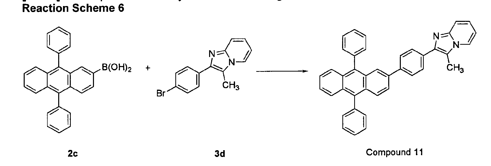
-
Compound 11 was prepared using Intermediate 2c prepared in the same manner as in Synthesis Example 2 and Intermediate 3d prepared in the same manner as in Synthesis Example 3. 4.72 g (Yield: 72%) ofCompound 11 that was light yellow powder was obtained through a Suzuki reaction between Intermediate 2c 5 g (13.36 mmol) and 3.49 g (12.15 mmol) of Intermediate 3d. The resulting compound was evaluated by NMR analysis with the following results: 1H NMR (400MHz, CDCl3) 7.97 (1H), 7.91 (1H), 7.85 (2H), 7.80 (1H), 7.73-7.70 (2H), 7.69 (1H), 7.66-7.61 (7H), 7.58 (2H), 7.56-7.50 (4H), 7.34 (2H), 7.19 (1H), 6.86 (1 H), 2.67 (3H) - Compound 12 was synthesized according to Reaction Scheme 7.

- Intermediate 1d was prepared in the same manner as in Synthesis Example 1, and then, 5 g of Intermediate 1d, 4.5 g of pyrene-1-yl-1-boronic acid, 0.46 g of tetrakis(triphenylphosphine)paladium, 6 g of potassium carbonate were dissolved in a solvent mixture including 80 ml of THF and 80 ml of water. The resultant mixture was stirred at a reflux temperature for 18 hours. The reaction product was cooled to room temperature and a first organic layer was separated. 80 ml of dichloromethane was added to an aqueous layer to extract a second organic layer. The first and second organic layers were put together and dried with magnesium sulfate to remove the solvent used, thereby obtaining a crude product. The crude product was refined by silica-gel-column chromatography to obtain 5.5 g of Compound 12. The resulting compound was evaluated by NMR analysis with the following results: 1H NMR (DMSO-d6, 400MHz) δ (ppm) 8.56 (1H, d), 8.51 (1H, s), 8.36 (1H, d), 8.31 (1H, d), 8.28 (1H, d), 8.22∼8.18 (6H, m), 8.10∼8.05 (2H, m), 7.70 (2H, d), 7.61 (1H, d), 7.26 (1H, t), 6.91 (1H, t)
- Compound 14 was synthesized according to Reaction Scheme 8:

- Intermediate 4d was prepared in the same manner as in Synthesis Example 4, and then, 2.9 g of Intermediate 4d, 2.0 g of pyrene-1-yl-1-boronic acid, 1.03 g of tetrakis(triphenylphosphine)palladium, and 13 g of potassium carbonate were dissolved in a solvent mixture including 40 ml of THF and 40 ml of water. The resultant mixture was stirred at a reflux temperature for 18 hours. The reaction product was cooled to room temperature and a first organic layer was separated. 40 ml of dichloromethane was added to an aqueous layer to extract a second organic layer. The first and second organic layers were put together and were dried with magnesium sulfate to remove the solvent used, thereby obtaining a crude product. The crude product was refined by silica-gel-column chromatography to obtain 3.0 g of Compound 14. The resulting compound was evaluated by NMR analysis with the following results: 1H NMR (DMSO-d6, 400MHz) d (ppm) 8.24∼8.13 (4H, m), 8.07 (2H, s), 8.01∼7.97 (4H, m), 7.89 (2H, d), 7.73 (1H, d), 7.57 (7H, br s), 7.22 (1H, t), 6.74 (1H, t)
-
Compound 17 was synthesized according to Reaction Scheme 9:
- Intermediate 7d was prepared in the same manner as in Synthesis Example 5, and then 3.94 g of Intermediate 7d, 3.0 g of pyrene-1-yl-1-boronic acid, 0.7 g of tetrakis(triphenylphosphine)palladium, and 8 g of potassium carbonate were dissolved in a solvent mixture including 70 ml of THF and 70 ml of water. The resultant mixture was stirred at a reflux temperature for 18 hours. The reaction product was cooled to room temperature and a first organic layer was separated. 70 ml of dichloromethane was added to an aqueous layer to extract a second organic layer. The first and second organic layers were put together and were dried with magnesium sulfate to remove the solvent used, thereby obtaining a crude product. The crude product was refined by silica-gel-column chromatography to obtain 3.7 g of
Compound 17. The resulting compound was evaluated by NMR analysis with the following results: 1H NMR (DMSO-d6, 400MHz) d (ppm) 8.59 (1H, d), 8.56 (1H, s), 8.41 (1H, d), 8.40 (1H, d), 8.34 (1H, d), 8.32 (1H, d), 8.27∼8.19 (6H, m), 8.13∼8.10 (2H, m), 7.91 (1H, d), 7.75 (2H, d), 7.72∼7.66 (2H, m), 7.31 (1H, d) - Compound 36 was synthesized according to Reaction Scheme 10:


- Intermediates 1a, 1b and 1c were synthesized in the same manner as in Synthesis Example 1.
- 3.39 g (35.98 mmol) of 2-aminopyrimidine and 10 g (35.98 mmol) of 2,4'-dibromoacetophenone were dissolved in 150 ml of ethanol and the mixture was refluxed for 12 hours. The reaction product was cooled to room temperature to form a white solid. The white solid was filtered and washed with a NaHCO3 -saturated solution. The residual humidity of an organic layer was removed with anhydrous magnesium sulfate, and dried under a reduced pressure. Then the resultant organic layer was re-crystallized with dichloromethane and normalhexane, thereby obtaining 8.02 g (Yield: 82%) of Intermediate 36d having a plate crystalline state.
- 1.85 g (3.90 mmol) of Intermediate 1c and 1g (3.90 mmol) of Intermediate 36d were added to a solution mixture of 2.7 g (19.5 mmol) of potassium carbonate solution and THF, and then 225 mg (0.196 mmol) of Pd(PPh3)4 was added thereto while stirring. The resultant mixture was refluxed for 6 hours. The reaction product was cooled to room temperature to form a solid compound, and the solid compound was filtered and washed with water, ethanol, and toluene, thereby obtaining 1.73 g (Yield: 71 %) of Compound 36. The resulting compound was evaluated by NMR analysis with the following results: 1H NMR (400MHz, CDCl3) 8.51 (1H), 8.40 (1H), 8.12 (1H), 8.06-7.99 (5H), 7.96 (2H), 7.85 (1H), 7.78-7.59 (15H), 7.32 (2H), 6.84 (1H)
-
Compound 37 was prepared in the same manner as in Synthesis Example 10, except that phenylmagnesiumbromide was used instead of 2-naphthylmagnesiumbromide used to form Intermediate 1 b in Synthesis Example 10. The resulting compound was evaluated by NMR analysis with the following results: 1H NMR (400MHz, CDCl3) 8.54 (1H), 8.42 (1H), 8.07 (2H), 7.96 (1H), 7.83 (1H), 7.80 (1H), 7.73-7.48 (15H), 7.35 (2H), 6.87 (1H) -
Compound 38 was prepared in the same manner as in Synthesis Example 10 for preparing Compound 36, except that phenylmagnesiumbromide was used instead of 2-naphthylmagnesiumbromide used to prepare Intermediate 1 b in Synthesis Example 10 and 2,4'-dibromopropiophenone was used instead of 2,4'-dibromoacetophenone used to prepare Intermediate 36d. The resulting compound was evaluated by NMR analysis with the following results: 1H NMR (400MHz, CDCl3) 8.54 (1H), 8.22 (1H), 7.97 (1H), 7.93 (2H), 7.70 (1H), 7.71-7.52 (15H), 7.35 (2H), 6.92 (1H), 2.73 (3H) - Compound 45 was synthesized according to Reaction Scheme 11:

- Intermediate 36d was prepared in the same manner as in Synthesis Example 10, and then 3.3 g of Intermediate 36d, 3 g of pyrene-1-yl-1-boronic acid, 0.7 g of tetrakis(triphenylphosphin)palladium, and 8 g of potassium carbonate were dissolved in a solvent mixture including 70 ml of THF and 70 ml of water. The resultant mixture was stirred at a reflux temperature for 18 hours. The reaction mixture was cooled to room temperature. Then a solid product in an organic layer was filtered and washed with a solvent mixture including water and THF, thereby obtaining 2.7 g of Compound 45. The resulting compound was evaluated by NMR analysis with the following results: 1H NMR (DMSO-d6, 400MHz) d (ppm) 9.01 (1H, dd), 8.56 (1H, q), 8.51 (1H, s), 8.39 (1H, d), 8.32 (2H, q), 8.25∼8.19 (6H, m), 8.10 (2H, t), 7.75 (2H, d), 7.09 (1H, dd)
- Compound 1 prepared according to Synthesis Example 1 was vacuum-deposited on a substrate to form a light-efficiency-improvement layer having a thickness of 600 Å. Then an anode was disposed on the light-efficiency-improvement layer by forming a 15 Ω/cm2 (1200 A) ITO. Then, m-MTDATA was vacuum-deposited on the anode to form an HIL having a thickness of 750 Å and then α-NPD was vacuum-deposited on the HIL to form an HTL having a thickness of 150 Å. An EML having a thickness of 300 Å was formed on the HTL by using 97 weight% of DSA constituting a host and 3 weight% of TBPe as a dopant. Then Alq3 was vacuum-deposited on the EML to form an ETL having a thickness of 200 Å. Then LiF was vacuum-deposited on the ETL to form an EIL having a thickness of 80 Å and then Al was vacuum-deposited on the EIL to form a cathode having a thickness of 3000 Å, thereby completing the manufacture of an organic light emitting diode.
- Organic light emitting diodes were manufactured in the same manner as in Example 1, except that Compounds 2, 3, 4, 7, 11, 36, 37 and 38 were used instead of Compound 1 to form the light-efficiency-improvement layer.
- An organic light emitting diode was manufactured in the same manner as in Example 1, except that Alq3 was used instead of Compound 1 to form the light-efficiency-improvement layer.
- Efficiency (cd/A) of each organic light emitting diodes prepared according to Examples 1 through 8 and Comparative Example was measured with a PR650 Spectroscan Source Measurement Unit. (produced by PhotoResearch Co.). The results are shown in Table 1.
Table 1 Example No. Light-efficiency-improvement layer forming compound Device efficiency (cd/A) Example 1 Compound 1 3.8 Example 3 Compound 3 3.6 Example 4 Compound 4 3.6 Example 5 Compound 7 3.5 Example 9 Compound 383.5 Example 7 Compound 36 3.6 Example 8 Compound 373.6 Comparative Example Alq3 3.1 - As described in the embodiments of the present invention, an organic light emitting diode including a light-efficiency-improvement layer containing the compound represented by Formula 1 has excellent light efficiency.
- While the present invention has been particularly shown and described with reference to exemplary embodiments thereof, it will be understood by those of ordinary skill in the art that various changes in form and details may be made therein without departing from the scope of the present invention as defined by the following claims.
Claims (21)
- An organic light emitting diode comprising:a substrate;a first electrode defining first and second surfaces opposite one another, the second surface facing the substrate;an organic layer facing the first surface of the first electrode;a second electrode defining first and second surfaces opposite one another, the first surface facing the organic layer; anda light-efficiency-improvement layer in contact with at least one of the second surface of the first electrode or the second surface of the second electrode and comprising a compound represented by Formula 1:
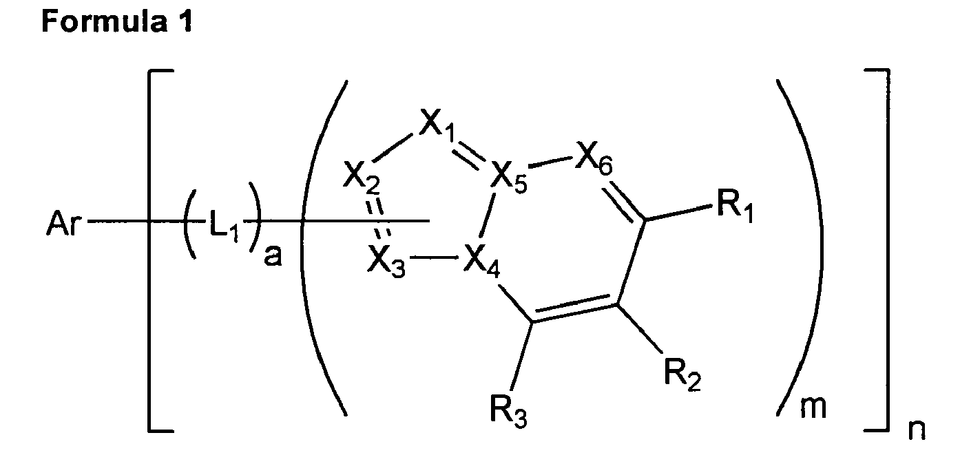 Ar is a substituted or unsubstituted C5-C30 aromatic ring system or a substituted or unsubstituted C2-C30 hetero aromatic ring system;each L1 is independently selected from the group consisting of substituted or unsubstituted C1-C30 alkylene groups, substituted or unsubstituted C5-C30 arylene groups, and substituted or unsubstituted C2-C30 hetero arylene groups;X1 is N, CY1, or a carbon atom bonded to L1 or Ar;X2 is N, CY2, or a carbon atom bonded to L1 or Ar;X3 is N, CY3, or a carbon atom bonded to L1 or Ar;X4 is N;X5 is a carbon atom;X6 is N or CY6;
wherein one of X1 through X6 is a carbon atom bonded to L1 or Ar;
each of R1 through R3 and Y1 through Y6 is independently selected from the group consisting of a hydrogen atom, halogen atoms, a hydroxyl group, a cyano group, substituted or unsubstituted C1-C30 alkyl groups, substituted or unsubstituted C1-C30 alkoxy groups, substituted or unsubstituted C1-C30 acyl groups, substituted or unsubstituted C2-C30 alkenyl groups, substituted or unsubstituted C2-C30 alkynyl groups, substituted or unsubstituted C5-C30 aryl groups, and substituted or unsubstituted C2-C30 hetero aryl groups, wherein two or more adjacent substituents selected from R1 through R3 and Y1 through Y6 may be bonded to each other to form a saturated or unsaturated ring;a is an integer from 0 to 10;m is an integer from 1 to 5; andn is an integer from 1 to 10. - An organic light emitting diode according to claim 1, wherein Ar is selected from the group consisting of substituted or unsubstituted pentalenes, substituted or unsubstituted indenes, substituted or unsubstituted naphthalenes, substituted or unsubstituted azulenes, a substituted or unsubstituted heptalenes, substituted or unsubstituted indacenes, substituted or unsubstituted acenaphthylenes, substituted or unsubstituted fluorenes, substituted or unsubstituted phenalenes, substituted or unsubstituted phenanthrenes, substituted or unsubstituted anthracenes, substituted or unsubstituted fluoranthenes, substituted or unsubstituted triphenylenes, substituted or unsubstituted pyrenes, substituted or unsubstituted chrysenes, substituted or unsubstituted naphthacenes, substituted or unsubstituted picenes, substituted or unsubstituted perylenes, substituted or unsubstituted pentaphenes, substituted or unsubstituted hexacenes, substituted or unsubstituted pyrroles, substituted or unsubstituted pyrazoles, substituted or unsubstituted imidazoles, substituted or unsubstituted imidazolines, substituted or unsubstituted pyridines, substituted or unsubstituted pyrazines, substituted or unsubstituted pyrimidines, substituted or unsubstituted indoles, substituted or unsubstituted purines, substituted or unsubstituted quinolines, substituted or unsubstituted phthalazines, substituted or unsubstituted indolizines, substituted or unsubstituted naphthyridines, substituted or unsubstituted quinazolines, substituted or unsubstituted cinnolines, substituted or unsubstituted indazoles, substituted or unsubstituted carbazoles, substituted or unsubstituted phenazines, substituted or unsubstituted phenanthridines, substituted or unsubstituted pyrans, substituted or unsubstituted chromenes, substituted or unsubstituted benzofurans, substituted or unsubstituted thiophenes, substituted or unsubstituted benzothiophenes, substituted or unsubstituted isothiazoles, and substituted or unsubstituted isoxazoles.
- An organic light emitting diode according to claim or claim 2, wherein, when Ar is a substituted C5-C30 aromatic ring system or a substituted C2-C30 hetero aromatic ring system, at least one substituent is selected from the group consisting of substituted or unsubstituted C6-C14 aryl groups and substituted or unsubstituted C2-C14 hetero aryl groups.
- An organic light emitting diode according to claim or claim 2, wherein, when Ar is a substituted C5-C30 aromatic ring system or a substituted C2-C30 hetero aromatic ring system, at least one substituent is selected from the group consisting of phenyl groups, halophenyl groups, C1-C10 alkylphenyl groups, C1-C10 alkoxyphenyl groups, naphthyl groups, halonaphthyl groups, C1-C10 alkylnaphthyl groups, C1-C10 alkoxynaphthyl groups, pyridinyl groups, halopyridinyl groups, C1-C10 alkylpyridinyl groups, C1-C10 alkoxypyridinyl groups, quinolinyl groups, haloquinolinyl groups, C1-C10 alkylquinolinyl groups, C1-C10 alkoxyquinolinyl groups, isoquinolinyl groups, haloisoquinolinyl groups, C1-C10 alkylisoquinolinyl groups, and C1-C10 alkoxyisoquinolinyl groups.
- An organic light emitting diode according to any preceding claim, wherein each L1 is independently selected from the group consisting of substituted or unsubstituted C6-C14 arylene groups and substituted or unsubstituted C2-C14 hetero arylene groups.
- An organic light emitting diode according to any preceding claim, wherein each L1 is independently selected from the group consisting of phenylene groups, halophenylene groups, C1-C10 alkylphenylene groups, C1-C10 alkoxyphenylene groups, naphthylene groups, halonaphthylene groups, C1-C10 alkylnaphthylene groups, and C1-C10 alkoxynaphthylene groups.
- An organic light emitting diode according to any of claims 1 to 4, wherein -(L1)a- is represented by any one formula selected from Formulae 2a through 2g:


- An organic light emitting diode according to any preceding claim, wherein at least one of X1, X4 and X6 is N.
- An organic light emitting diode according to claim 8, wherein each of X1 and X4 is N.
- An organic light emitting diode according to claim 8, wherein each of X1, X4 and X6 is N.
- An organic light emitting diode according to any preceding claim, wherein each of R1 through R3 and Y1 through Y6 is independently selected from the group consisting of a hydrogen atom, substituted or unsubstituted C1-C10 alkyl groups, substituted or unsubstituted C2-C10 alkenyl groups, substituted or unsubstituted C6-C14 aryl groups, and substituted or unsubstituted C2-C14 hetero aryl groups.
- An organic light emitting diode according to any of claims 1 to 11, wherein each of R1 through R3 and Y1 through Y6 is independently selected from the group consisting of a hydrogen atom, C1-C10 alkyl groups, C1-C10 halo alkyl groups, C2-C10 alkenyl groups, C2-C10 halo alkenyl groups, phenyl groups, halophenyl groups, C1-C10 alkylphenyl groups, C1-C10 alkoxyphenyl groups, naphthyl groups, halonaphthyl groups, C1-C10 alkyl naphthyl groups, and C1-C10 alkoxynaphthyl groups.
- An organic light emitting diode according to any preceding claim, wherein n is 1 or 2.
- An organic light emitting diode according to claim 1, wherein the compound represented by Formula 1 is a compound represented by any one formula selected from Formulae 1A through 1X:


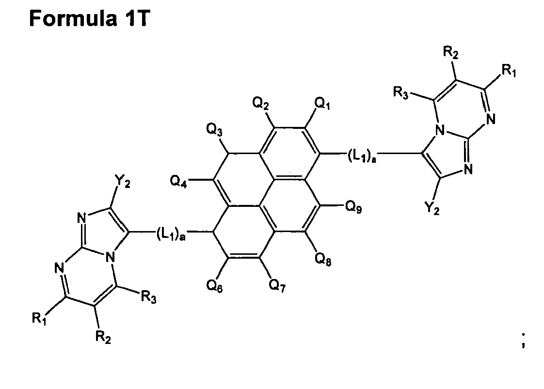


each of Q1 through Q11 is independently selected from the group consisting of a hydrogen atom, substituted or unsubstituted C6-C14 aryl groups, and substituted or unsubstituted C2-C14 hetero aryl groups;
each of L1 is independently selected from the group consisting of substituted or unsubstituted C6-C14 arylene groups and substituted or unsubstituted C2-C14 hetero arylene groups;
each of R1, R2, R3, Y2 and Y3 is independently selected from the group consisting of a hydrogen atom, substituted or unsubstituted C1-C10 alkyl groups, substituted or unsubstituted C2-C10 alkenyl groups, substituted or unsubstituted C6-C14 aryl groups, and C2-C14 hetero aryl groups, wherein two or more adjacent substituents selected from R1, R2, R3, Y2 and Y3 may be bonded to each other to form a C6-C12 aromatic ring; and
a is 1 or 2. - An organic light emitting diode according to claim 14, wherein Q1 through Q11 are each independently a hydrogen atom, a phenyl group, a halophenyl group, a C1-C10 alkylphenyl group, a C1-C10 alkoxyphenyl group, a naphthyl group, a halonaphthyl group, a C1-C10 alkylnaphthyl group, a C1-C10 alkoxynaphthyl group, a pyridinyl group, a halopyridinyl group, a C1-C10 alkylpyridinyl group, a C1-C10 alkoxypyridinyl group, a quinolinyl group, a haloquinolinyl group, a C1-C10 alkylquinolinyl group, a C1-C10 alkoxyquinolinyl group, an isoquinolinyl group, a haloisoquinolinyl group, a C1-C10 alkylisoquinolinyl group, or a C1-C10 alkoxyisoquinolinyl group.
- An organic light emitting diode according to any preceding claim, wherein the second electrode is a transmission-type electrode and the light-efficiency-improvement layer is in contact with the second surface of the second electrode.
- An organic light emitting diode according to any preceding claim, wherein the first electrode is a transmission-type electrode and the light-efficiency-improvement layer is in contact with the second surface of the first electrode.
- An organic light emitting diode according to any preceding claim, wherein the first electrode and the second electrode are transmission-type electrodes and a light-efficiency-improvement layer is in contact with the second surface of the first electrode and a light-efficiency-improvement layer is in contact with the second surface of the second electrode.
- An organic light emitting according to any preceding claim, wherein the organic layer is individually formed corresponding to R, G and B pixels and the light-efficiency-improvement layer is a common layer with respect to the R, G and B pixels.
- An organic light emitting diode according to any of claims 1-18, wherein the organic layer is individually formed corresponding to R, G and B pixels and the light-efficiency-improvement layer comprises at least one layer selected from the group consisting of a light-efficiency-improvement layer-R formed corresponding to the R pixel, a light-efficiency-improvement layer-G formed corresponding to the G pixel, and a light-efficiency-improvement layer-B formed corresponding to the B pixel.
- An organic light emitting diode according to claim 19, wherein the light-efficiency-improvement layer comprises the light-efficiency-improvement layer-R, the light-efficiency-improvement layer- G, and the light-efficiency-improvement layer-B.
Applications Claiming Priority (1)
| Application Number | Priority Date | Filing Date | Title |
|---|---|---|---|
| KR1020080080567A KR100994115B1 (en) | 2008-08-18 | 2008-08-18 | Organic light emitting device having a light efficiency improving layer |
Publications (2)
| Publication Number | Publication Date |
|---|---|
| EP2157627A1 true EP2157627A1 (en) | 2010-02-24 |
| EP2157627B1 EP2157627B1 (en) | 2013-01-23 |
Family
ID=41258751
Family Applications (1)
| Application Number | Title | Priority Date | Filing Date |
|---|---|---|---|
| EP09252012A Active EP2157627B1 (en) | 2008-08-18 | 2009-08-18 | Organic light emitting diode including light-efficiency-improvement layer |
Country Status (6)
| Country | Link |
|---|---|
| US (1) | US8343638B2 (en) |
| EP (1) | EP2157627B1 (en) |
| JP (1) | JP4949443B2 (en) |
| KR (1) | KR100994115B1 (en) |
| CN (1) | CN101656300B (en) |
| TW (1) | TWI392720B (en) |
Cited By (1)
| Publication number | Priority date | Publication date | Assignee | Title |
|---|---|---|---|---|
| EP3089232A4 (en) * | 2013-12-26 | 2017-06-21 | Toray Industries, Inc. | Organic light-emitting element |
Families Citing this family (25)
| Publication number | Priority date | Publication date | Assignee | Title |
|---|---|---|---|---|
| KR101182444B1 (en) * | 2010-04-01 | 2012-09-12 | 삼성디스플레이 주식회사 | Organic light emitting diode comprising the same |
| JP5315420B2 (en) * | 2010-07-09 | 2013-10-16 | 出光興産株式会社 | IMIDAZOPYRIDINE DERIVATIVE AND ORGANIC ELECTROLUMINESCENT DEVICE COMPRISING THE SAME |
| JP5979947B2 (en) * | 2011-04-12 | 2016-08-31 | ユー・ディー・シー アイルランド リミテッド | ORGANIC ELECTROLUMINESCENT ELEMENT, COMPOUND USED FOR THE ELEMENT, LIGHT EMITTING DEVICE, DISPLAY DEVICE AND LIGHTING DEVICE USING THE ELEMENT |
| KR101181281B1 (en) * | 2012-03-13 | 2012-09-10 | 덕산하이메탈(주) | An organic electronic element comprising a layer for improving light efficiency, a electronic device comprising the same, and compound used for the same |
| CN103664937B (en) * | 2012-08-30 | 2016-06-29 | 昆山维信诺显示技术有限公司 | A kind of quinoline [7,8-h] quinolines and application thereof |
| CN103709180B (en) * | 2012-09-29 | 2016-12-21 | 昆山维信诺显示技术有限公司 | Containing the condensed-nuclei aromatics derivant of imidazo [1,2-a] pyridine groups and the application in OLED thereof |
| CN103788087B (en) * | 2012-10-30 | 2017-05-10 | 昆山维信诺显示技术有限公司 | Anthracene derivatives containing imidazo[1,2,a]pyridine group and applications thereof in OLEDs |
| KR102098093B1 (en) | 2012-12-06 | 2020-04-08 | 덕산네오룩스 주식회사 | Compound for organic electronic element, organic electronic element using the same, and an electronic device thereof |
| KR102077776B1 (en) * | 2013-05-22 | 2020-02-17 | 덕산네오룩스 주식회사 | An organic electronic element comprising a layer for improving light efficiency, and an electronic device comprising the same |
| KR102231935B1 (en) * | 2013-08-05 | 2021-03-25 | 덕산네오룩스 주식회사 | Organic electric element comprising compound for organic electric element and electronic device thereof |
| WO2015020348A1 (en) * | 2013-08-05 | 2015-02-12 | 덕산하이메탈(주) | Organic electrical element using compound for organic electrical element, and electronic device therefor |
| KR102177211B1 (en) * | 2013-12-05 | 2020-11-11 | 삼성디스플레이 주식회사 | Organic light emitting device |
| CN104650117B (en) * | 2013-12-26 | 2017-08-01 | 北京鼎材科技有限公司 | A kind of organic compound and its application in organic electroluminescence device |
| CN104650116B (en) * | 2013-12-26 | 2017-12-05 | 北京鼎材科技有限公司 | A kind of organic compound and its application in organic electroluminescence device |
| KR102163320B1 (en) * | 2014-04-10 | 2020-10-08 | 덕산네오룩스 주식회사 | Compound for organic electronic element, organic electronic element using the same, and an electronic device thereof |
| KR102208247B1 (en) * | 2014-05-29 | 2021-01-27 | 덕산네오룩스 주식회사 | Organic electronic element using a compound for organic electronic element, and an electronic device thereof |
| KR102249062B1 (en) * | 2014-11-28 | 2021-05-10 | 덕산네오룩스 주식회사 | Compound for organic electronic element, organic electronic element using the same, and an electronic device thereof |
| KR102396300B1 (en) | 2014-12-30 | 2022-05-11 | 삼성디스플레이 주식회사 | An organic light emitting device employing a layer for improving a light efficiency |
| KR102706485B1 (en) * | 2016-11-14 | 2024-09-12 | 삼성디스플레이 주식회사 | Light emitting diode |
| EP3765459A1 (en) | 2018-03-13 | 2021-01-20 | Shire Human Genetic Therapies, Inc. | Substituted imidazopyridines as inhibitors of plasma kallikrein and uses thereof |
| CN108503646A (en) * | 2018-03-27 | 2018-09-07 | 上海道亦化工科技有限公司 | A kind of Pyrazolopyrimidine compound and application thereof and luminescent device |
| CN108484608A (en) * | 2018-03-28 | 2018-09-04 | 上海道亦化工科技有限公司 | A kind of Pyrazolopyrimidine compound and application thereof and luminescent device |
| CN108847447B (en) * | 2018-07-12 | 2022-09-09 | 长春海谱润斯科技股份有限公司 | Top-emitting organic electroluminescent device |
| DK4031547T3 (en) | 2019-09-18 | 2024-09-09 | Takeda Pharmaceuticals Co | PLASMA KALLIKREIN INHIBITORS AND USES THEREOF |
| EP4031245A1 (en) | 2019-09-18 | 2022-07-27 | Takeda Pharmaceutical Company Limited | Heteroaryl plasma kallikrein inhibitors |
Citations (3)
| Publication number | Priority date | Publication date | Assignee | Title |
|---|---|---|---|---|
| US6737800B1 (en) * | 2003-02-18 | 2004-05-18 | Eastman Kodak Company | White-emitting organic electroluminescent device with color filters and reflective layer for causing colored light constructive interference |
| EP1925618A1 (en) * | 2006-11-24 | 2008-05-28 | Samsung SDI Co., Ltd. | Imidazopyridine-based compounds and organic light emitting diode including organic layer comprising the imidazopyridine-based compounds |
| KR100852118B1 (en) * | 2007-03-13 | 2008-08-13 | 삼성에스디아이 주식회사 | An imidazopyrimidine compound and an organic light emitting device comprising an organic film |
Family Cites Families (8)
| Publication number | Priority date | Publication date | Assignee | Title |
|---|---|---|---|---|
| EP1582516B1 (en) * | 2003-01-10 | 2013-07-17 | Idemitsu Kosan Co., Ltd. | Nitrogenous heterocyclic derivative and organic electroluminescent element employing the same |
| JP4481930B2 (en) * | 2003-07-11 | 2010-06-16 | 出光興産株式会社 | White organic electroluminescence device |
| KR100968191B1 (en) * | 2004-11-16 | 2010-07-06 | 인터내셔널 비지네스 머신즈 코포레이션 | Organic Light-Emitting Devices Including Dielectric Capping Layers |
| US20070104977A1 (en) | 2005-11-07 | 2007-05-10 | Idemitsu Kosan Co., Ltd. | Organic electroluminescent device |
| KR100721953B1 (en) * | 2005-11-30 | 2007-05-25 | 삼성에스디아이 주식회사 | Full color organic light emitting display device and manufacturing method thereof |
| KR101230316B1 (en) | 2006-03-21 | 2013-02-06 | 삼성디스플레이 주식회사 | Display device and manufacturing method of the same |
| KR100903102B1 (en) * | 2006-11-24 | 2009-06-16 | 삼성모바일디스플레이주식회사 | An imidazopyridine-based compound and an organic light emitting diode employing an organic layer comprising the same |
| KR100958641B1 (en) * | 2008-08-18 | 2010-05-20 | 삼성모바일디스플레이주식회사 | Organic light emitting device having a light efficiency improving layer |
-
2008
- 2008-08-18 KR KR1020080080567A patent/KR100994115B1/en active Active
-
2009
- 2009-08-17 CN CN200910163380XA patent/CN101656300B/en active Active
- 2009-08-17 JP JP2009188534A patent/JP4949443B2/en not_active Expired - Fee Related
- 2009-08-17 TW TW098127565A patent/TWI392720B/en not_active IP Right Cessation
- 2009-08-18 US US12/543,334 patent/US8343638B2/en active Active
- 2009-08-18 EP EP09252012A patent/EP2157627B1/en active Active
Patent Citations (3)
| Publication number | Priority date | Publication date | Assignee | Title |
|---|---|---|---|---|
| US6737800B1 (en) * | 2003-02-18 | 2004-05-18 | Eastman Kodak Company | White-emitting organic electroluminescent device with color filters and reflective layer for causing colored light constructive interference |
| EP1925618A1 (en) * | 2006-11-24 | 2008-05-28 | Samsung SDI Co., Ltd. | Imidazopyridine-based compounds and organic light emitting diode including organic layer comprising the imidazopyridine-based compounds |
| KR100852118B1 (en) * | 2007-03-13 | 2008-08-13 | 삼성에스디아이 주식회사 | An imidazopyrimidine compound and an organic light emitting device comprising an organic film |
Non-Patent Citations (2)
| Title |
|---|
| WANG, L:, LING, Y., CHANG, C., DUAN, L. AND QIU, Y.: "Research on the adhesive ability between ITO anode and PET substrate improved by polyimide buffer layer", CHINESE SCIENCE BULLETIN, vol. 50, no. 6, 2005, pages 505 - 508, XP002555403 * |
| ZHU X ET AL: "High-performance top-emitting white organic light-emitting devices", JAPANESE JOURNAL OF APPLIED PHYSICS, JAPAN SOCIETY OF APPLIED PHYSICS, TOKYO,JP, vol. 46, no. 7A, 1 July 2007 (2007-07-01), pages 4054 - 4058, XP001517970, ISSN: 0021-4922 * |
Cited By (2)
| Publication number | Priority date | Publication date | Assignee | Title |
|---|---|---|---|---|
| EP3089232A4 (en) * | 2013-12-26 | 2017-06-21 | Toray Industries, Inc. | Organic light-emitting element |
| US10483488B2 (en) | 2013-12-26 | 2019-11-19 | Toray Industries, Inc. | Organic light-emitting element |
Also Published As
| Publication number | Publication date |
|---|---|
| CN101656300B (en) | 2013-10-09 |
| TWI392720B (en) | 2013-04-11 |
| JP4949443B2 (en) | 2012-06-06 |
| KR20100021907A (en) | 2010-02-26 |
| JP2010045033A (en) | 2010-02-25 |
| EP2157627B1 (en) | 2013-01-23 |
| KR100994115B1 (en) | 2010-11-15 |
| TW201016825A (en) | 2010-05-01 |
| US8343638B2 (en) | 2013-01-01 |
| US20100039029A1 (en) | 2010-02-18 |
| CN101656300A (en) | 2010-02-24 |
Similar Documents
| Publication | Publication Date | Title |
|---|---|---|
| EP2157627B1 (en) | Organic light emitting diode including light-efficiency-improvement layer | |
| KR101722027B1 (en) | A condensed-cyclic compound and an organic light emitting diode comprising the same | |
| EP1925618B1 (en) | Imidazopyridine-based compounds and organic light emitting diode including organic layer comprising the imidazopyridine-based compounds | |
| KR101528241B1 (en) | An aromatic cyclic compound, an organic light emitting device having an organic film containing the same, and a method for manufacturing the organic light emitting device | |
| EP2298741B1 (en) | 1H-benzo[g]indole compounds and organic luminescence device using the same | |
| EP2289877B1 (en) | Organic light emitting device containing polycyclic heteroaryl compounds | |
| EP2554545B1 (en) | Carbazole-based compound and organic light-emitting diode comprising the same | |
| EP2292618B1 (en) | Organic light emitting device containing polycyclic heteroaryl compounds | |
| JP5823731B2 (en) | Organic light emitting device | |
| EP2110373B1 (en) | Bipyridine-based compound and organic light emitting diode employing organic layer comprising the same | |
| EP2292601B1 (en) | Phenanthro[2,3-b]pyrroles and Phenanthro[3,2-b]pyrroles for organic light-emitting devices | |
| TWI642756B (en) | Carbazole-based compound and organic light-emitting diode comprising the same | |
| KR102098736B1 (en) | Compound for organic light emitting device and organic light emitting device comprising the same | |
| TWI596096B (en) | Compound, organic light-emitting device comprising the same, and flat display device comprising the same | |
| KR101853875B1 (en) | Heterocyclic compound and organic light emitting device containing same | |
| KR20130100633A (en) | Pyrene-based compound, organic light emitting diode comprising the same and organic light emitting apparatus comprising the same | |
| EP2392563B1 (en) | Nitrogen containing polycyclic derivatives useful in organic light-emitting devices | |
| KR102052071B1 (en) | Organic light emitting device | |
| TWI614236B (en) | Novel compound with electron injection and/or electron transport capabilities and organic light-emitting device including the same | |
| EP2301920A1 (en) | Organic light emitting device containing naphthoindole derivatives | |
| KR102087950B1 (en) | Heterocyclic compound and organic light emitting device comprising the same | |
| KR101940103B1 (en) | Novel heterocyclic compound and organic light emitting device containing same | |
| KR101736987B1 (en) | Heterocyclic compound and organic light emitting device comprising the same | |
| KR20150068144A (en) | Compound and organic light emitting device comprising same | |
| EP2772493B1 (en) | Condensed benzoindoles and organic light emitting device comprising the same |
Legal Events
| Date | Code | Title | Description |
|---|---|---|---|
| PUAI | Public reference made under article 153(3) epc to a published international application that has entered the european phase |
Free format text: ORIGINAL CODE: 0009012 |
|
| 17P | Request for examination filed |
Effective date: 20090826 |
|
| AK | Designated contracting states |
Kind code of ref document: A1 Designated state(s): AT BE BG CH CY CZ DE DK EE ES FI FR GB GR HR HU IE IS IT LI LT LU LV MC MK MT NL NO PL PT RO SE SI SK SM TR |
|
| AX | Request for extension of the european patent |
Extension state: AL BA RS |
|
| REG | Reference to a national code |
Ref country code: DE Ref legal event code: R079 Ref document number: 602009012975 Country of ref document: DE Free format text: PREVIOUS MAIN CLASS: H01L0051000000 Ipc: H01L0051540000 |
|
| GRAP | Despatch of communication of intention to grant a patent |
Free format text: ORIGINAL CODE: EPIDOSNIGR1 |
|
| RIC1 | Information provided on ipc code assigned before grant |
Ipc: H01L 51/54 20060101AFI20120723BHEP |
|
| RAP1 | Party data changed (applicant data changed or rights of an application transferred) |
Owner name: SAMSUNG DISPLAY CO., LTD. |
|
| GRAS | Grant fee paid |
Free format text: ORIGINAL CODE: EPIDOSNIGR3 |
|
| GRAA | (expected) grant |
Free format text: ORIGINAL CODE: 0009210 |
|
| RIN1 | Information on inventor provided before grant (corrected) |
Inventor name: YANG, SEUNG-GAK, Inventor name: LEE, JONG-HYUK, Inventor name: KIM, HEE-YEON, Inventor name: LEE, JAE-YONG, |
|
| AK | Designated contracting states |
Kind code of ref document: B1 Designated state(s): AT BE BG CH CY CZ DE DK EE ES FI FR GB GR HR HU IE IS IT LI LT LU LV MC MK MT NL NO PL PT RO SE SI SK SM TR |
|
| REG | Reference to a national code |
Ref country code: GB Ref legal event code: FG4D |
|
| REG | Reference to a national code |
Ref country code: CH Ref legal event code: EP |
|
| REG | Reference to a national code |
Ref country code: AT Ref legal event code: REF Ref document number: 595376 Country of ref document: AT Kind code of ref document: T Effective date: 20130215 Ref country code: CH Ref legal event code: EP |
|
| REG | Reference to a national code |
Ref country code: IE Ref legal event code: FG4D |
|
| REG | Reference to a national code |
Ref country code: DE Ref legal event code: R096 Ref document number: 602009012975 Country of ref document: DE Effective date: 20130321 |
|
| REG | Reference to a national code |
Ref country code: AT Ref legal event code: MK05 Ref document number: 595376 Country of ref document: AT Kind code of ref document: T Effective date: 20130123 |
|
| REG | Reference to a national code |
Ref country code: LT Ref legal event code: MG4D |
|
| REG | Reference to a national code |
Ref country code: NL Ref legal event code: VDEP Effective date: 20130123 |
|
| PG25 | Lapsed in a contracting state [announced via postgrant information from national office to epo] |
Ref country code: BE Free format text: LAPSE BECAUSE OF FAILURE TO SUBMIT A TRANSLATION OF THE DESCRIPTION OR TO PAY THE FEE WITHIN THE PRESCRIBED TIME-LIMIT Effective date: 20130123 Ref country code: IS Free format text: LAPSE BECAUSE OF FAILURE TO SUBMIT A TRANSLATION OF THE DESCRIPTION OR TO PAY THE FEE WITHIN THE PRESCRIBED TIME-LIMIT Effective date: 20130523 Ref country code: BG Free format text: LAPSE BECAUSE OF FAILURE TO SUBMIT A TRANSLATION OF THE DESCRIPTION OR TO PAY THE FEE WITHIN THE PRESCRIBED TIME-LIMIT Effective date: 20130423 Ref country code: AT Free format text: LAPSE BECAUSE OF FAILURE TO SUBMIT A TRANSLATION OF THE DESCRIPTION OR TO PAY THE FEE WITHIN THE PRESCRIBED TIME-LIMIT Effective date: 20130123 Ref country code: NO Free format text: LAPSE BECAUSE OF FAILURE TO SUBMIT A TRANSLATION OF THE DESCRIPTION OR TO PAY THE FEE WITHIN THE PRESCRIBED TIME-LIMIT Effective date: 20130423 Ref country code: LT Free format text: LAPSE BECAUSE OF FAILURE TO SUBMIT A TRANSLATION OF THE DESCRIPTION OR TO PAY THE FEE WITHIN THE PRESCRIBED TIME-LIMIT Effective date: 20130123 Ref country code: ES Free format text: LAPSE BECAUSE OF FAILURE TO SUBMIT A TRANSLATION OF THE DESCRIPTION OR TO PAY THE FEE WITHIN THE PRESCRIBED TIME-LIMIT Effective date: 20130504 Ref country code: SE Free format text: LAPSE BECAUSE OF FAILURE TO SUBMIT A TRANSLATION OF THE DESCRIPTION OR TO PAY THE FEE WITHIN THE PRESCRIBED TIME-LIMIT Effective date: 20130123 |
|
| PG25 | Lapsed in a contracting state [announced via postgrant information from national office to epo] |
Ref country code: SI Free format text: LAPSE BECAUSE OF FAILURE TO SUBMIT A TRANSLATION OF THE DESCRIPTION OR TO PAY THE FEE WITHIN THE PRESCRIBED TIME-LIMIT Effective date: 20130123 Ref country code: PL Free format text: LAPSE BECAUSE OF FAILURE TO SUBMIT A TRANSLATION OF THE DESCRIPTION OR TO PAY THE FEE WITHIN THE PRESCRIBED TIME-LIMIT Effective date: 20130123 Ref country code: FI Free format text: LAPSE BECAUSE OF FAILURE TO SUBMIT A TRANSLATION OF THE DESCRIPTION OR TO PAY THE FEE WITHIN THE PRESCRIBED TIME-LIMIT Effective date: 20130123 Ref country code: PT Free format text: LAPSE BECAUSE OF FAILURE TO SUBMIT A TRANSLATION OF THE DESCRIPTION OR TO PAY THE FEE WITHIN THE PRESCRIBED TIME-LIMIT Effective date: 20130523 Ref country code: LV Free format text: LAPSE BECAUSE OF FAILURE TO SUBMIT A TRANSLATION OF THE DESCRIPTION OR TO PAY THE FEE WITHIN THE PRESCRIBED TIME-LIMIT Effective date: 20130123 Ref country code: NL Free format text: LAPSE BECAUSE OF FAILURE TO SUBMIT A TRANSLATION OF THE DESCRIPTION OR TO PAY THE FEE WITHIN THE PRESCRIBED TIME-LIMIT Effective date: 20130123 Ref country code: GR Free format text: LAPSE BECAUSE OF FAILURE TO SUBMIT A TRANSLATION OF THE DESCRIPTION OR TO PAY THE FEE WITHIN THE PRESCRIBED TIME-LIMIT Effective date: 20130424 |
|
| PG25 | Lapsed in a contracting state [announced via postgrant information from national office to epo] |
Ref country code: HR Free format text: LAPSE BECAUSE OF FAILURE TO SUBMIT A TRANSLATION OF THE DESCRIPTION OR TO PAY THE FEE WITHIN THE PRESCRIBED TIME-LIMIT Effective date: 20130123 |
|
| PG25 | Lapsed in a contracting state [announced via postgrant information from national office to epo] |
Ref country code: EE Free format text: LAPSE BECAUSE OF FAILURE TO SUBMIT A TRANSLATION OF THE DESCRIPTION OR TO PAY THE FEE WITHIN THE PRESCRIBED TIME-LIMIT Effective date: 20130123 Ref country code: CZ Free format text: LAPSE BECAUSE OF FAILURE TO SUBMIT A TRANSLATION OF THE DESCRIPTION OR TO PAY THE FEE WITHIN THE PRESCRIBED TIME-LIMIT Effective date: 20130123 Ref country code: RO Free format text: LAPSE BECAUSE OF FAILURE TO SUBMIT A TRANSLATION OF THE DESCRIPTION OR TO PAY THE FEE WITHIN THE PRESCRIBED TIME-LIMIT Effective date: 20130123 Ref country code: DK Free format text: LAPSE BECAUSE OF FAILURE TO SUBMIT A TRANSLATION OF THE DESCRIPTION OR TO PAY THE FEE WITHIN THE PRESCRIBED TIME-LIMIT Effective date: 20130123 Ref country code: SK Free format text: LAPSE BECAUSE OF FAILURE TO SUBMIT A TRANSLATION OF THE DESCRIPTION OR TO PAY THE FEE WITHIN THE PRESCRIBED TIME-LIMIT Effective date: 20130123 |
|
| PG25 | Lapsed in a contracting state [announced via postgrant information from national office to epo] |
Ref country code: CY Free format text: LAPSE BECAUSE OF FAILURE TO SUBMIT A TRANSLATION OF THE DESCRIPTION OR TO PAY THE FEE WITHIN THE PRESCRIBED TIME-LIMIT Effective date: 20130123 |
|
| PLBE | No opposition filed within time limit |
Free format text: ORIGINAL CODE: 0009261 |
|
| STAA | Information on the status of an ep patent application or granted ep patent |
Free format text: STATUS: NO OPPOSITION FILED WITHIN TIME LIMIT |
|
| PG25 | Lapsed in a contracting state [announced via postgrant information from national office to epo] |
Ref country code: IT Free format text: LAPSE BECAUSE OF FAILURE TO SUBMIT A TRANSLATION OF THE DESCRIPTION OR TO PAY THE FEE WITHIN THE PRESCRIBED TIME-LIMIT Effective date: 20130123 |
|
| 26N | No opposition filed |
Effective date: 20131024 |
|
| REG | Reference to a national code |
Ref country code: DE Ref legal event code: R097 Ref document number: 602009012975 Country of ref document: DE Effective date: 20131024 |
|
| REG | Reference to a national code |
Ref country code: CH Ref legal event code: PL |
|
| PG25 | Lapsed in a contracting state [announced via postgrant information from national office to epo] |
Ref country code: CH Free format text: LAPSE BECAUSE OF NON-PAYMENT OF DUE FEES Effective date: 20130831 Ref country code: MC Free format text: LAPSE BECAUSE OF FAILURE TO SUBMIT A TRANSLATION OF THE DESCRIPTION OR TO PAY THE FEE WITHIN THE PRESCRIBED TIME-LIMIT Effective date: 20130123 Ref country code: LI Free format text: LAPSE BECAUSE OF NON-PAYMENT OF DUE FEES Effective date: 20130831 |
|
| REG | Reference to a national code |
Ref country code: IE Ref legal event code: MM4A |
|
| PG25 | Lapsed in a contracting state [announced via postgrant information from national office to epo] |
Ref country code: IE Free format text: LAPSE BECAUSE OF NON-PAYMENT OF DUE FEES Effective date: 20130818 |
|
| PG25 | Lapsed in a contracting state [announced via postgrant information from national office to epo] |
Ref country code: SM Free format text: LAPSE BECAUSE OF FAILURE TO SUBMIT A TRANSLATION OF THE DESCRIPTION OR TO PAY THE FEE WITHIN THE PRESCRIBED TIME-LIMIT Effective date: 20130123 |
|
| PG25 | Lapsed in a contracting state [announced via postgrant information from national office to epo] |
Ref country code: TR Free format text: LAPSE BECAUSE OF FAILURE TO SUBMIT A TRANSLATION OF THE DESCRIPTION OR TO PAY THE FEE WITHIN THE PRESCRIBED TIME-LIMIT Effective date: 20130123 Ref country code: MT Free format text: LAPSE BECAUSE OF FAILURE TO SUBMIT A TRANSLATION OF THE DESCRIPTION OR TO PAY THE FEE WITHIN THE PRESCRIBED TIME-LIMIT Effective date: 20130123 |
|
| PG25 | Lapsed in a contracting state [announced via postgrant information from national office to epo] |
Ref country code: HU Free format text: LAPSE BECAUSE OF FAILURE TO SUBMIT A TRANSLATION OF THE DESCRIPTION OR TO PAY THE FEE WITHIN THE PRESCRIBED TIME-LIMIT; INVALID AB INITIO Effective date: 20090818 Ref country code: LU Free format text: LAPSE BECAUSE OF NON-PAYMENT OF DUE FEES Effective date: 20130818 Ref country code: MK Free format text: LAPSE BECAUSE OF FAILURE TO SUBMIT A TRANSLATION OF THE DESCRIPTION OR TO PAY THE FEE WITHIN THE PRESCRIBED TIME-LIMIT Effective date: 20130123 |
|
| REG | Reference to a national code |
Ref country code: FR Ref legal event code: PLFP Year of fee payment: 8 |
|
| REG | Reference to a national code |
Ref country code: FR Ref legal event code: PLFP Year of fee payment: 9 |
|
| REG | Reference to a national code |
Ref country code: FR Ref legal event code: PLFP Year of fee payment: 10 |
|
| REG | Reference to a national code |
Ref country code: DE Ref legal event code: R079 Ref document number: 602009012975 Country of ref document: DE Free format text: PREVIOUS MAIN CLASS: H01L0051540000 Ipc: H10K0085000000 |
|
| P01 | Opt-out of the competence of the unified patent court (upc) registered |
Effective date: 20230515 |
|
| PGFP | Annual fee paid to national office [announced via postgrant information from national office to epo] |
Ref country code: DE Payment date: 20240722 Year of fee payment: 16 |
|
| PGFP | Annual fee paid to national office [announced via postgrant information from national office to epo] |
Ref country code: GB Payment date: 20240723 Year of fee payment: 16 |
|
| PGFP | Annual fee paid to national office [announced via postgrant information from national office to epo] |
Ref country code: FR Payment date: 20240723 Year of fee payment: 16 |
|
| REG | Reference to a national code |
Ref country code: DE Ref legal event code: R119 Ref document number: 602009012975 Country of ref document: DE |