EP2154731A1 - Photodetector and display device provided with same - Google Patents
Photodetector and display device provided with same Download PDFInfo
- Publication number
- EP2154731A1 EP2154731A1 EP08765516A EP08765516A EP2154731A1 EP 2154731 A1 EP2154731 A1 EP 2154731A1 EP 08765516 A EP08765516 A EP 08765516A EP 08765516 A EP08765516 A EP 08765516A EP 2154731 A1 EP2154731 A1 EP 2154731A1
- Authority
- EP
- European Patent Office
- Prior art keywords
- layer
- photodiode
- light
- electrode
- metal layer
- Prior art date
- Legal status (The legal status is an assumption and is not a legal conclusion. Google has not performed a legal analysis and makes no representation as to the accuracy of the status listed.)
- Granted
Links
Images





Classifications
-
- G—PHYSICS
- G02—OPTICS
- G02F—OPTICAL DEVICES OR ARRANGEMENTS FOR THE CONTROL OF LIGHT BY MODIFICATION OF THE OPTICAL PROPERTIES OF THE MEDIA OF THE ELEMENTS INVOLVED THEREIN; NON-LINEAR OPTICS; FREQUENCY-CHANGING OF LIGHT; OPTICAL LOGIC ELEMENTS; OPTICAL ANALOGUE/DIGITAL CONVERTERS
- G02F1/00—Devices or arrangements for the control of the intensity, colour, phase, polarisation or direction of light arriving from an independent light source, e.g. switching, gating or modulating; Non-linear optics
- G02F1/01—Devices or arrangements for the control of the intensity, colour, phase, polarisation or direction of light arriving from an independent light source, e.g. switching, gating or modulating; Non-linear optics for the control of the intensity, phase, polarisation or colour
- G02F1/13—Devices or arrangements for the control of the intensity, colour, phase, polarisation or direction of light arriving from an independent light source, e.g. switching, gating or modulating; Non-linear optics for the control of the intensity, phase, polarisation or colour based on liquid crystals, e.g. single liquid crystal display cells
- G02F1/133—Constructional arrangements; Operation of liquid crystal cells; Circuit arrangements
- G02F1/13306—Circuit arrangements or driving methods for the control of single liquid crystal cells
- G02F1/13318—Circuits comprising a photodetector
-
- H—ELECTRICITY
- H10—SEMICONDUCTOR DEVICES; ELECTRIC SOLID-STATE DEVICES NOT OTHERWISE PROVIDED FOR
- H10F—INORGANIC SEMICONDUCTOR DEVICES SENSITIVE TO INFRARED RADIATION, LIGHT, ELECTROMAGNETIC RADIATION OF SHORTER WAVELENGTH OR CORPUSCULAR RADIATION
- H10F30/00—Individual radiation-sensitive semiconductor devices in which radiation controls the flow of current through the devices, e.g. photodetectors
- H10F30/20—Individual radiation-sensitive semiconductor devices in which radiation controls the flow of current through the devices, e.g. photodetectors the devices having potential barriers, e.g. phototransistors
- H10F30/21—Individual radiation-sensitive semiconductor devices in which radiation controls the flow of current through the devices, e.g. photodetectors the devices having potential barriers, e.g. phototransistors the devices being sensitive to infrared, visible or ultraviolet radiation
- H10F30/22—Individual radiation-sensitive semiconductor devices in which radiation controls the flow of current through the devices, e.g. photodetectors the devices having potential barriers, e.g. phototransistors the devices being sensitive to infrared, visible or ultraviolet radiation the devices having only one potential barrier, e.g. photodiodes
- H10F30/223—Individual radiation-sensitive semiconductor devices in which radiation controls the flow of current through the devices, e.g. photodetectors the devices having potential barriers, e.g. phototransistors the devices being sensitive to infrared, visible or ultraviolet radiation the devices having only one potential barrier, e.g. photodiodes the potential barrier being a PIN barrier
-
- H—ELECTRICITY
- H10—SEMICONDUCTOR DEVICES; ELECTRIC SOLID-STATE DEVICES NOT OTHERWISE PROVIDED FOR
- H10F—INORGANIC SEMICONDUCTOR DEVICES SENSITIVE TO INFRARED RADIATION, LIGHT, ELECTROMAGNETIC RADIATION OF SHORTER WAVELENGTH OR CORPUSCULAR RADIATION
- H10F77/00—Constructional details of devices covered by this subclass
- H10F77/10—Semiconductor bodies
- H10F77/14—Shape of semiconductor bodies; Shapes, relative sizes or dispositions of semiconductor regions within semiconductor bodies
- H10F77/147—Shapes of bodies
-
- H—ELECTRICITY
- H10—SEMICONDUCTOR DEVICES; ELECTRIC SOLID-STATE DEVICES NOT OTHERWISE PROVIDED FOR
- H10F—INORGANIC SEMICONDUCTOR DEVICES SENSITIVE TO INFRARED RADIATION, LIGHT, ELECTROMAGNETIC RADIATION OF SHORTER WAVELENGTH OR CORPUSCULAR RADIATION
- H10F77/00—Constructional details of devices covered by this subclass
- H10F77/30—Coatings
- H10F77/306—Coatings for devices having potential barriers
- H10F77/331—Coatings for devices having potential barriers for filtering or shielding light, e.g. multicolour filters for photodetectors
- H10F77/334—Coatings for devices having potential barriers for filtering or shielding light, e.g. multicolour filters for photodetectors for shielding light, e.g. light blocking layers or cold shields for infrared detectors
-
- H—ELECTRICITY
- H10—SEMICONDUCTOR DEVICES; ELECTRIC SOLID-STATE DEVICES NOT OTHERWISE PROVIDED FOR
- H10F—INORGANIC SEMICONDUCTOR DEVICES SENSITIVE TO INFRARED RADIATION, LIGHT, ELECTROMAGNETIC RADIATION OF SHORTER WAVELENGTH OR CORPUSCULAR RADIATION
- H10F77/00—Constructional details of devices covered by this subclass
- H10F77/30—Coatings
- H10F77/306—Coatings for devices having potential barriers
- H10F77/331—Coatings for devices having potential barriers for filtering or shielding light, e.g. multicolour filters for photodetectors
- H10F77/337—Coatings for devices having potential barriers for filtering or shielding light, e.g. multicolour filters for photodetectors using interference filters, e.g. multilayer dielectric filters
-
- G—PHYSICS
- G02—OPTICS
- G02F—OPTICAL DEVICES OR ARRANGEMENTS FOR THE CONTROL OF LIGHT BY MODIFICATION OF THE OPTICAL PROPERTIES OF THE MEDIA OF THE ELEMENTS INVOLVED THEREIN; NON-LINEAR OPTICS; FREQUENCY-CHANGING OF LIGHT; OPTICAL LOGIC ELEMENTS; OPTICAL ANALOGUE/DIGITAL CONVERTERS
- G02F1/00—Devices or arrangements for the control of the intensity, colour, phase, polarisation or direction of light arriving from an independent light source, e.g. switching, gating or modulating; Non-linear optics
- G02F1/01—Devices or arrangements for the control of the intensity, colour, phase, polarisation or direction of light arriving from an independent light source, e.g. switching, gating or modulating; Non-linear optics for the control of the intensity, phase, polarisation or colour
- G02F1/13—Devices or arrangements for the control of the intensity, colour, phase, polarisation or direction of light arriving from an independent light source, e.g. switching, gating or modulating; Non-linear optics for the control of the intensity, phase, polarisation or colour based on liquid crystals, e.g. single liquid crystal display cells
- G02F1/133—Constructional arrangements; Operation of liquid crystal cells; Circuit arrangements
- G02F1/13306—Circuit arrangements or driving methods for the control of single liquid crystal cells
- G02F1/13312—Circuits comprising photodetectors for purposes other than feedback
-
- G—PHYSICS
- G02—OPTICS
- G02F—OPTICAL DEVICES OR ARRANGEMENTS FOR THE CONTROL OF LIGHT BY MODIFICATION OF THE OPTICAL PROPERTIES OF THE MEDIA OF THE ELEMENTS INVOLVED THEREIN; NON-LINEAR OPTICS; FREQUENCY-CHANGING OF LIGHT; OPTICAL LOGIC ELEMENTS; OPTICAL ANALOGUE/DIGITAL CONVERTERS
- G02F1/00—Devices or arrangements for the control of the intensity, colour, phase, polarisation or direction of light arriving from an independent light source, e.g. switching, gating or modulating; Non-linear optics
- G02F1/01—Devices or arrangements for the control of the intensity, colour, phase, polarisation or direction of light arriving from an independent light source, e.g. switching, gating or modulating; Non-linear optics for the control of the intensity, phase, polarisation or colour
- G02F1/13—Devices or arrangements for the control of the intensity, colour, phase, polarisation or direction of light arriving from an independent light source, e.g. switching, gating or modulating; Non-linear optics for the control of the intensity, phase, polarisation or colour based on liquid crystals, e.g. single liquid crystal display cells
- G02F1/133—Constructional arrangements; Operation of liquid crystal cells; Circuit arrangements
- G02F1/136—Liquid crystal cells structurally associated with a semi-conducting layer or substrate, e.g. cells forming part of an integrated circuit
- G02F1/1362—Active matrix addressed cells
-
- G—PHYSICS
- G02—OPTICS
- G02F—OPTICAL DEVICES OR ARRANGEMENTS FOR THE CONTROL OF LIGHT BY MODIFICATION OF THE OPTICAL PROPERTIES OF THE MEDIA OF THE ELEMENTS INVOLVED THEREIN; NON-LINEAR OPTICS; FREQUENCY-CHANGING OF LIGHT; OPTICAL LOGIC ELEMENTS; OPTICAL ANALOGUE/DIGITAL CONVERTERS
- G02F2201/00—Constructional arrangements not provided for in groups G02F1/00 - G02F7/00
- G02F2201/58—Arrangements comprising a monitoring photodetector
-
- Y—GENERAL TAGGING OF NEW TECHNOLOGICAL DEVELOPMENTS; GENERAL TAGGING OF CROSS-SECTIONAL TECHNOLOGIES SPANNING OVER SEVERAL SECTIONS OF THE IPC; TECHNICAL SUBJECTS COVERED BY FORMER USPC CROSS-REFERENCE ART COLLECTIONS [XRACs] AND DIGESTS
- Y02—TECHNOLOGIES OR APPLICATIONS FOR MITIGATION OR ADAPTATION AGAINST CLIMATE CHANGE
- Y02E—REDUCTION OF GREENHOUSE GAS [GHG] EMISSIONS, RELATED TO ENERGY GENERATION, TRANSMISSION OR DISTRIBUTION
- Y02E10/00—Energy generation through renewable energy sources
- Y02E10/50—Photovoltaic [PV] energy
Definitions
- the present invention relates to a photodetector and a display device provided with the same.
- a display device represented by a liquid crystal display device often is equipped with a photo sensor for automatically adjusting brightness of a display screen in accordance with the intensity of light surrounding the display device.
- a display device having a plurality of photo sensors arranged in a matrix also has been known.
- the plural photo sensors function as one area sensor, thereby capturing an image at the observer side.
- the incorporation of the photo sensor in the display device can be achieved by mounting a photo sensor as a discrete component on a display panel thereof.
- a photo sensor can be formed monolithically on an active matrix substrate by utilizing a process for forming an active element (TFT) or a peripheral circuit.
- TFT active element
- the photo sensor is required to be formed monolithically on the active matrix substrate, from the viewpoint of reducing the number of components and downsizing the display device.
- a photodiode formed of a silicon layer for instance, is known (see, for instance, JP 2006-3857 A : FIGs. 2 and 3 ).
- FIG. 12 is a cross-sectional view showing a configuration of a liquid crystal display panel having a photodiode.
- a photodiode 51 is a PIN diode having a lateral structure, which is formed monolithically on an active matrix substrate 50 that forms a liquid crystal display panel.
- the photodiode 51 includes a silicon layer 60.
- the silicon layer 60 is formed on a glass substrate 52 as the base substrate of the active matrix substrate 50, by utilizing a process of forming a thin film transistor (TFT) that functions as an active element, at the same time of forming the TFT.
- TFT thin film transistor
- an n-type semiconductor region (n-layer) 51a, an intrinsic semiconductor region (i-layer) 51b and a p-type semiconductor region (p-layer) 51c are formed in this order along the planar direction.
- the i-layer 51b serves as a photodetection region of the photodiode 51.
- a light-shielding layer 53 for shielding light from a backlight device (not shown) is provided on an under layer of the photodiode 51.
- the light-shielding layer 53 is covered with an insulating base coat 54.
- the light-shielding layer 53 is formed of a metal material.
- the light-shielding layer 53 is in an electrically suspended state, insulated from the ambience.
- the photodiode 51 is covered further with interlayer insulating layers 55 and 56.
- numeral 57 denotes a wiring connected to the n-layer 51a
- 58 denotes a wiring connected to the p-layer 51c
- Numeral 59 denotes a flattening layer
- 61 denotes a protective layer
- Numeral 62 denotes a liquid crystal layer. For a filter substrate 63, only the appearance is shown.
- the metal light-shielding layer 53 is arranged on the under layer of the photodiode 51, the output characteristics of the photodiode 51 fluctuate with the fluctuation in an electric potential of the light-shielding layer 53. And the electric potential of the light-shielding layer 53 fluctuates in connection with the fluctuation in an electric potential of the photodiode p-layer 51c.
- the light-shielding layer 53, the photodiode 51 and the other films positioned in the vicinity of the photodiode 51 contain a fixed charge captured during the formation process.
- the amount of the fixed charge varies among the photodiodes or the active matrix substrates, and the difference in the fixed charge results in the difference in the relationship between the electric potential of the light-shielding layer 53 and the output characteristics of the photodiode.
- the output characteristics may vary among the photodiodes even though an equal voltage is applied to the respective p-layers 51c and the electric potentials in the respective light-shielding layers are set to be equivalent.
- the relationship between the electric potential of the light-shielding layer 53 and the output characteristics of the photodiode will vary due to not only the fixed charge but the variations in the diffusion concentration of impurities in the semiconductor regions of the photodiode 51. Similarly to the above-described case, the output characteristics may be varied among the photodiodes even though an equivalent voltage is applied to the respective p-layers 51c.
- the output characteristics vary among the photodiodes. Specifically for instance, the output characteristics are different from one product to another even for the photodiodes of the same specification. Alternatively, the output characteristics are different from one photodiode to another even for photodiodes of the same specification mounted on the same active matrix substrate. In such a case, it will be difficult to adjust the brightness of the display screen with the photo sensor or to capture a high-resolution picture.
- An object of the present invention is to provide a photodetector capable of solve the above-mentioned problems and suppressing variations in the output characteristics among the photodiodes, and a display device provided with the photodetector.
- a photodetector is characterized in that it includes a transparency base substrate, a metal layer provided on one main surface of the base substrate, a photodiode arranged on an upper layer of the metal layer, and an electrode arranged in the vicinity of the photodiode on the upper layer of the metal layer, wherein the photodiode comprises a silicon layer having a semiconductor region, the silicon layer is insulated electrically from the metal layer; the electrode is insulated electrically from the metal layer and the silicon layer; and the metal layer is formed so that a part of the metal layer is overlapped with the silicon layer and the other part of the metal layer is overlapped with the electrode in the thickness direction of the base substrate.
- a display device is characterized in that it has an active matrix substrate, wherein the active matrix substrate comprises a transparency base substrate, a plurality of active elements formed on one main surface of the base substrate, and a photodetector, where the photodetector comprises a metal layer provided on one main surface of the base substrate, a photodiode arranged on an upper layer of the metal layer, and an electrode arranged in the vicinity of the photodiode on the upper layer of the metal layer; the photodiode comprises a silicon layer having a semiconductor region, the silicon layer is insulated electrically from the metal layer; the electrode is insulated electrically from the metal layer and the silicon layer; and the metal layer is formed so that a part of the metal layer is overlapped with the silicon layer and the other part of the metal layer is overlapped with the electrode in the thickness direction of the base substrate.
- the active matrix substrate comprises a transparency base substrate, a plurality of active elements formed on one main surface of the base substrate, and a photodetector, where the photodet
- the metal layer to form a light-shielding layer for the photodiode spreads to the under layer of the electrode arranged in the vicinity of the photodiode, and thus the electric potential of the light-shielding layer (metal layer) can be adjusted by applying the electrode with voltage. Further, the relationship between the electric potential of the light-shielding layer and the output characteristics of the photodiode can be controlled by adjusting the electric potential of the light-shielding layer, thereby a problem that the output characteristics vary among the photodiodes even if the voltages applied to the photodiodes are equivalent can be avoided. Therefore, according to the present invention, variations in the output characteristics among the photodiodes can be suppressed.
- a photodetector is characterized in that it includes a transparency base substrate, a metal layer provided on one main surface of the base substrate, a photodiode arranged on an upper layer of the metal layer, and an electrode arranged in the vicinity of the photodiode on the upper layer of the metal layer, wherein the photodiode comprises a silicon layer having a semiconductor region, the silicon layer is insulated electrically from the metal layer; the electrode is insulated electrically from the metal layer and the silicon layer; and the metal layer is formed so that a part of the metal layer is overlapped with the silicon layer and the other part of the metal layer is overlapped with the electrode in the thickness direction of the base substrate.
- a display device is characterized in that it has an active matrix substrate, wherein the active matrix substrate comprises a transparency base substrate, a plurality of active elements formed on one main surface of the base substrate, and a photodetector, where the photodetector comprises a metal layer provided on one main surface of the base substrate, a photodiode arranged on an upper layer of the metal layer, and an electrode arranged in the vicinity of the photodiode on the upper layer of the metal layer; the photodiode comprises a silicon layer having a semiconductor region, the silicon layer is insulated electrically from the metal layer; the electrode is insulated electrically from the metal layer and the silicon layer; and the metal layer is formed so that a part of the metal layer is overlapped with the silicon layer and the other part of the metal layer is overlapped with the electrode in the thickness direction of the base substrate.
- the silicon layer includes a p-type semiconductor region, an intrinsic semiconductor region and an n-type semiconductor region, and that the p-type semiconductor region, the intrinsic semiconductor region and the n-type semiconductor region are adjacent to each other in the planar direction of the silicon layer.
- the electrode can be a part of a wiring connected to any of the plurality of active elements.
- the electrode can be a part of a gate wiring connected to a gate electrode of the transistor element or a part of a source wiring.
- FIG. 1 is a cross-sectional view showing a schematic configuration of a photodetector according to the embodiment of the present invention.
- FIG. 2 is a plan view showing from above the photodetector shown in FIG. 1 .
- FIG. 3 is a plan view showing a schematic configuration of a part of the display device provided with the photodetector shown in FIG.1 .
- FIG.1 only the conductive and semi-conductive members for forming an active matrix substrate 20 as described below are hatched.
- FIGs. 2 and 3 show the main components only.
- a photodetector according to the present embodiment is provided to the active matrix substrate 20.
- the active matrix substrate 20 composes a part of the display device according to the present embodiment.
- the display device according to the present embodiment is a liquid crystal display device, which is formed by interposing a liquid crystal layer 21 between the active matrix substrate 20 and a filter substrate 22.
- the filter substrate 22 is shown only in the appearance. Though not shown, the filter substrate 22 is provided with a counter electrode and a color filter.
- a plurality of thin film transistors (TFTs) 15 are formed on the active matrix substrate 20.
- the TFTs 15 are arranged in a matrix together with transparency pixel electrodes 16 on one main surface of the base substrate 2 (see FIG. 1 ).
- the TFTs 15 function as active elements for turning on and off the pixel electrodes 16.
- One TFT 15 and one pixel electrode 16 compose one sub-pixel, and one pixel is composed of a set of three sub-pixels. The three sub-pixels composing one pixel are different from each other in the color of the corresponding color filters.
- each of the TFTs 15 is provided with a silicon layer 15a on which a source region and a drain region are formed, and a gate electrode 15b.
- the gate electrode 15b is formed integrally with a gate wiring 13 arranged along the horizontal direction of a screen.
- a source electrode 17 is connected to the source region, and a drain electrode 18 is connected to the drain region.
- the source electrode 17 is formed integrally with a source wiring 14 arranged along the vertical direction of the screen.
- the drain electrode 18 is connected to the pixel electrode 16.
- the photodetector includes the transparency base substrate 2, a metal layer 3 provided on a main surface of the base substrate 2, a photodiode 1 arranged on an upper layer of the metal layer 3, and an electrode 12 also arranged on the upper layer of the metal layer 3.
- the base substrate 2 composes a part of the active matrix substrate 20.
- the metal layer 3 is a light-shielding layer provided to prevent incidence of light from a backlight device into the photodiode 1 (hereinafter referred to as "light-shielding layer 3").
- the light-shielding layer 3 is insulated electrically in the entire circumference so that it is in an electrically suspended state.
- the photodiode 1 includes a silicon layer 11 having a semiconductor region.
- the silicon layer 11 is formed on an insulating layer 4 that covers the light-shielding layer 3, and insulated electrically from the light-shielding layer 3.
- the photodiode 1 is a PIN diode having a lateral structure.
- an n-type semiconductor region (n-layer) 11a, an intrinsic semiconductor region (i-layer) 11b and a p-type semiconductor region (p-layer) 11c are provided in this order.
- the i-layer 11b serves as the photodetection region of the photodiode 1.
- the n-layer 11a, the i-layer 11b and the p-layer 11c are formed adjacent to each other in the planar direction of the silicon layer 11.
- the i-layer 11b is not limited particularly as long as it is electrically neutral in comparison with the adjacent n-layer 11a and the p-layer 11c. It is preferable that the i-layer 11b is completely free of impurities and/or it is a region where the conduction electron density and the hole density are equal to each other. Alternatively however, the i-layer 11b can be an n- region where the diffusion concentration of the n-type impurity is lower than that of the n-layer 11a, or a p- region where the diffusion concentration of the p-type impurity is lower than that of the p-layer 11c.
- the type of the silicon composing the silicon layer 11 is not limited particularly.
- the silicon layer 11 is formed preferably of a continuous grain boundary silicon or a low-temperature polysilicon. It is also preferable that the silicon layer 11 is formed by using the process for forming the TFT 15 (see FIG. 3 ).
- the electrode 12 is formed in the vicinity of the photodiode 1 so as to be electrically insulated from both the light-shielding layer 3 and the silicon layer 11.
- the electrode 12 is formed on the interlayer insulating layer 5 that covers the silicon layer 11.
- the electrode 12 is insulated electrically from the silicon layer 11 by the interlayer insulating layer 5, and is insulated electrically from the light-shielding layer 3 by both the insulating layer 4 and the interlayer insulating layer 5.
- the electrode 12 is adjacent to the silicon layer 11 when viewed from above.
- an interlayer insulating layer 6 is formed further to cover the electrode 12.
- the light-shielding layer 3 is formed so that a part thereof is overlapped with the silicon layer 11 and the other part is overlapped with the electrode 12 in the thickness direction of the base substrate 2. Namely, the light-shielding layer 3 is formed to cover not only the region right below the silicon layer 11 but the region right below the electrode 12. In the present embodiment, only the i-layer 11b of the silicon layer 11 is the photodetection region.
- the light-shielding layer 3 is not limited particularly as long as it shields at least the i-layer 11b of the silicon layer 11.
- the light-shielding layer 3 is formed beyond the region right below the photodiode 1 according to the present embodiment, and the electrode 12 is formed further thereon. Therefore, the electric potential of the light-shielding layer (metal layer) 3 can be adjusted by applying a voltage to the electrode 12, and thus the relationship between the electric potential of the light-shielding layer 3 and the output characteristics of the photodiode 1 can be controlled.
- the electrode 12 composes a part of the gate wiring 13. Application of voltage to the electrode 12 is carried out when a corresponding gate wiring 13 is not selected. And the level of the voltage to be applied to the electrode 12 at this time is set to a value lower than the threshold voltage of the TFT 15 so as to prevent the TFT 15 (see FIG. 3 ) from being unnecessarily turned on.
- the electrode 12 is not limited to the above-described example as long as it composes a part of the wiring connected to any of the TFTs (active elements) 15.
- it can be a part of the source wiring connected to the TFT 15.
- a voltage signal is applied to the electrode 12 at a selected timing that the source wiring is not used for sending a display signal.
- numeral 9 denotes a flattening layer
- 10 denotes a protective layer
- Numeral 7 denotes a wiring connected to the n-layer 11a
- 8 denotes a wiring connected to the p-layer 11c.
- the wirings 7 and 8 are formed to penetrate the interlayer insulating layers 5, 6 and the flattening layer 9.
- the wirings 7 and 8 are not shown in FIG. 3 .
- FIGs. 4-6 are diagrams respectively showing the electric potentials of the light-shielding layers and the states of the photodiodes.
- FIGs. 4A , 5A and 6A show the flows of free electrons and positive holes
- FIGs. 4B , 5B and 6B show energy bands in the photodiodes
- FIGs. 4C , 5C and 6C show equivalent circuits.
- the electric potential V G of the light-shielding layer 3 in FIG. 4 satisfies the formula (1) below
- the same electric potential in FIG. 5 satisfies the formula (2) below
- the same electric potential in FIG. 6 satisfies the formula (3) below.
- V C denotes an electric potential in the n-layer 11a of the photodiode 1
- V A denotes an electric potential in the p-layer 11c of the photodiode 1.
- V th_n denotes a threshold voltage for a case of a n-channel MOS transistor having the n-layer 11a as a source-drain region, the light-shielding layer 3 as a gate electrode, and the insulating layer 4 as a gate insulating layer.
- V th_p denotes a threshold voltage for a case of a p-channel MOS transistor having the p-layer 11c as a source-drain region, the light-shielding layer 3 as a gate electrode, and the insulating layer 4 as a gate insulating layer.
- E C denotes an energy level in a conduction band
- E F denotes an energy level in a forbidden band
- E V denotes an energy level in a valence band.
- mode C in a case where the electric potential V G of the light-shielding layer 3 satisfies the above formula (3) (hereinafter, this case is referred to as "mode C"), transfer of the free electrons and the positive holes will occur easily only in the vicinity of the interface of the i-layer 11b at the p-layer 11c side. As shown in FIG. 6C , in the mode C, the current flow is hindered by the i-layer 11b similarly to the case of the mode B.
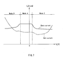
- FIG. 7 is a diagram showing the relationship between a photocurrent in the photodiode and the electric potential of the light-shielding layer.
- the y-axis indicates a current value [A/ ⁇ m] of a current outputted from the photodiode 1
- the x-axis indicates the electric potential V G [V] of the light-shielding layer 3.
- the photocurrent and the dark current of the photodiode 1 fluctuate depending on the electric potential V G of the light-shielding layer 3. And there is a tendency that the photocurrent increases the most and the dark current becomes the lowest at the time of the mode A as shown in FIG. 4 .
- the ratio of the photocurrent to the dark current S/N ratio
- the output characteristics of the photodiode 1 turns to be a preferable state. That is, as shown in FIGs. 4-7 , the output characteristics of the photodiode 1 fluctuate together with the fluctuation in the electric potential of the light-shielding layer 3.
- the photocurrent and the dark current fluctuate remarkably when there occurs a switchover between the modes. In light of this, it is preferable that a switchover from one mode to another does not occur.
- FIG. 7 shows only one example, and actually the mode A range varies among the photodiodes.
- the relationship between the electric potential V G of the light-shielding layer 3 and the output characteristics of the photodiode 1 varies among the photodiodes 1.
- the diffusion concentrations of the n-layer 11a and the p-layer 11c vary even among the photodiodes of the same specification, and thus variations exist in the threshold voltages V th_n and V th_p .
- the electric charge amount of the fixed charge contained in the photodiode 1, the light-shielding layer 3 and the like varies among the photodiodes.
- the variations in the range of the mode A will be described with reference to FIGs. 8-10 .
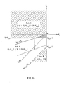
- FIGs. 8-10 are diagrams showing the respective ranges of the mode A to the mode C, which are different from each other in the relationship between the electric potentials of the light-shielding layers and the output characteristics of the photodiodes.
- the y-axis indicates the electric potential V G of the light-shielding layer
- the x-axis indicates the electric potential V A of the p-layer 11c.
- the electric potential V G of the light-shielding layer 3 will be discussed.
- capacitances are formed by the insulating layer 4.
- C gc the capacitance between the n-layer 11a and the light-shielding layer 3
- C ga the capacitance between the p-layer 11c and the light-shielding layer 3
- the electric potential V G of the light-shielding layer 3 can be approximated as shown in the formula (4) below by using the electric potential V A of the p-layer 11c.
- the ⁇ value becomes (1/2).
- the ⁇ value is not constant but it varies among the modes. Therefore in the example as shown in FIGs. 9 and 10 , the gradient of the straight line indicating the above formula (5) will vary among the modes.
- the region of the p-layer 11c is increased substantially as shown in FIG. 5 , and the C ga value becomes greater in comparison with the case of the mode A. Therefore in the mode B, the ⁇ value become greater and the gradient of the straight line indicating the above formula (5) becomes larger.
- the region of the n-layer 11a is increased substantially as shown in FIG. 6 , and the C gc value becomes greater in comparison with the case of the mode A. Therefore in the mode C, the ⁇ value become smaller and the gradient of the straight line indicating the above formula (5) becomes smaller.
- the fluctuation width of the actual ⁇ value is trivial, it is not shown in FIGs. 8-10 .
- FIGs. 8-10 will be reviewed.
- a straight line indicating the above formula (5) exists constantly within the range of the mode A irrespective of the electric potential V A of the p-layer 11c. Therefore in this case, the photodiode 1 is in the state of mode A constantly
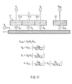
- FIG. 11 is an explanatory view showing the relationship between the light-shielding layer, the photodiode, and the electrode.
- the electrode 12 is arranged in the vicinity of the photodiode. Therefore, when the voltage V CTRL is applied to the electrode 12, an electric field is provided by the electrode 12 to the light-shielding layer 3, and thus the electric potential V G of the light-shielding layer 3 fluctuates.
- the electric potential V G of the light-shielding layer 3 can be expressed by the formula (6) below.
- the capacitance C CTRL denotes a capacitance formed between the electrode 12 and the light-shielding layer 3.
- the capacitance C gi denotes a capacitance formed between the i-layer 11b and the light-shielding layer 3 (see FIG. 11 ).
- V g0 denotes an electric potential that rises due to application of a voltage to the electrode 12.
- V g0 can be expressed by the formula (7) below.
- the electric potential V G of the light-shielding layer can be expressed by the formula (8) below.
- V g ⁇ 0 V CTRL ⁇ C CTRL C CTRL + C diode
- V G of the light-shielding layer 3 it is possible to adjust the electric potential V G of the light-shielding layer 3 by adjusting the voltage V CTRL applied to the electrode 12. Therefore for instance, in the example as shown in FIGs. 9 and 10 , by adjusting the voltage V CTRL , V g0 becomes an intercept of a straight line as indicated with the arrows of broken lines in these drawings, and thus the straight line can be translated. In this case, even when the electric potential V A of the p-layer 11c approaches zero, the photodiode 1 is still in the mode A.
- the photodetector and the display device by controlling the electric potential V G of the light-shielding layer 3 corresponding to the respective photodiodes 1, it is possible to suppress fluctuation in the output characteristics among the photodiodes 1. Namely, it is possible to avoid a situation that a part of the plural photodiodes of the same specification is in the mode A while the remaining part is in the mode B or the mode C during a reverse bias voltage of an equal electric potential is applied to the photodiodes 1.
- the display device is the liquid crystal display device
- the display device according to the present embodiment will not be limited to the example.
- the display device can be an organic EL display device or an inorganic EL display device for instance other than the liquid crystal display device.
- the photodetector of the present invention can be incorporated in a display device such as a liquid crystal display device or an EL display device.
- a display device of the present invention further can be used as a liquid crystal display device, an EL display device or the like.
- the photodetector and the display device of the present invention have industrial availability.
Landscapes
- Physics & Mathematics (AREA)
- Nonlinear Science (AREA)
- Mathematical Physics (AREA)
- Chemical & Material Sciences (AREA)
- Crystallography & Structural Chemistry (AREA)
- General Physics & Mathematics (AREA)
- Optics & Photonics (AREA)
- Light Receiving Elements (AREA)
- Solid State Image Pick-Up Elements (AREA)
- Liquid Crystal (AREA)
Abstract
Description
- The present invention relates to a photodetector and a display device provided with the same.
- Recently, a display device represented by a liquid crystal display device often is equipped with a photo sensor for automatically adjusting brightness of a display screen in accordance with the intensity of light surrounding the display device. A display device having a plurality of photo sensors arranged in a matrix also has been known. In this display device, the plural photo sensors function as one area sensor, thereby capturing an image at the observer side.
- The incorporation of the photo sensor in the display device can be achieved by mounting a photo sensor as a discrete component on a display panel thereof. Alternatively, a photo sensor can be formed monolithically on an active matrix substrate by utilizing a process for forming an active element (TFT) or a peripheral circuit.
- In the field of a display device for a mobile terminal device in particular, the photo sensor is required to be formed monolithically on the active matrix substrate, from the viewpoint of reducing the number of components and downsizing the display device. As the photo sensor formed monolithically, a photodiode formed of a silicon layer, for instance, is known (see, for instance,
JP 2006-3857 A FIGs. 2 and3 ). - Hereinafter, a conventional photodiode (photo sensor) will be explained with reference to
FIG. 12. FIG. 12 is a cross-sectional view showing a configuration of a liquid crystal display panel having a photodiode. As shown inFIG. 12 , aphotodiode 51 is a PIN diode having a lateral structure, which is formed monolithically on anactive matrix substrate 50 that forms a liquid crystal display panel. - As shown in
FIG. 12 , thephotodiode 51 includes asilicon layer 60. Thesilicon layer 60 is formed on aglass substrate 52 as the base substrate of theactive matrix substrate 50, by utilizing a process of forming a thin film transistor (TFT) that functions as an active element, at the same time of forming the TFT. Further on thesilicon layer 60, an n-type semiconductor region (n-layer) 51a, an intrinsic semiconductor region (i-layer) 51b and a p-type semiconductor region (p-layer) 51c are formed in this order along the planar direction. The i-layer 51b serves as a photodetection region of thephotodiode 51. - On an under layer of the
photodiode 51, a light-shielding layer 53 for shielding light from a backlight device (not shown) is provided. The light-shielding layer 53 is covered with aninsulating base coat 54. Typically the light-shielding layer 53 is formed of a metal material. The light-shielding layer 53 is in an electrically suspended state, insulated from the ambience. Thephotodiode 51 is covered further withinterlayer insulating layers - In
FIG. 12 ,numeral 57 denotes a wiring connected to the n-layer layer 51c. Numeral 59 denotes a flattening layer, and 61 denotes a protective layer. Numeral 62 denotes a liquid crystal layer. For afilter substrate 63, only the appearance is shown. - In the example as shown in
FIG. 12 , since the metal light-shielding layer 53 is arranged on the under layer of thephotodiode 51, the output characteristics of thephotodiode 51 fluctuate with the fluctuation in an electric potential of the light-shielding layer 53. And the electric potential of the light-shielding layer 53 fluctuates in connection with the fluctuation in an electric potential of the photodiode p-layer 51c. - However, the light-
shielding layer 53, thephotodiode 51 and the other films positioned in the vicinity of thephotodiode 51 contain a fixed charge captured during the formation process. The amount of the fixed charge varies among the photodiodes or the active matrix substrates, and the difference in the fixed charge results in the difference in the relationship between the electric potential of the light-shielding layer 53 and the output characteristics of the photodiode. Namely, in a case where a plurality ofphotodiodes 51 of the same specification are provided, the output characteristics may vary among the photodiodes even though an equal voltage is applied to the respective p-layers 51c and the electric potentials in the respective light-shielding layers are set to be equivalent. - The relationship between the electric potential of the light-
shielding layer 53 and the output characteristics of the photodiode will vary due to not only the fixed charge but the variations in the diffusion concentration of impurities in the semiconductor regions of thephotodiode 51. Similarly to the above-described case, the output characteristics may be varied among the photodiodes even though an equivalent voltage is applied to the respective p-layers 51c. - As mentioned above, in the example as shown in
FIG. 12 , a problem that the output characteristics vary among the photodiodes arises. Specifically for instance, the output characteristics are different from one product to another even for the photodiodes of the same specification. Alternatively, the output characteristics are different from one photodiode to another even for photodiodes of the same specification mounted on the same active matrix substrate. In such a case, it will be difficult to adjust the brightness of the display screen with the photo sensor or to capture a high-resolution picture. - An object of the present invention is to provide a photodetector capable of solve the above-mentioned problems and suppressing variations in the output characteristics among the photodiodes, and a display device provided with the photodetector.
- For achieving the above-described object, a photodetector according to the present invention is characterized in that it includes a transparency base substrate, a metal layer provided on one main surface of the base substrate, a photodiode arranged on an upper layer of the metal layer, and an electrode arranged in the vicinity of the photodiode on the upper layer of the metal layer, wherein the photodiode comprises a silicon layer having a semiconductor region, the silicon layer is insulated electrically from the metal layer; the electrode is insulated electrically from the metal layer and the silicon layer; and the metal layer is formed so that a part of the metal layer is overlapped with the silicon layer and the other part of the metal layer is overlapped with the electrode in the thickness direction of the base substrate.
- And, for achieving the above-described object, a display device according to the present invention is characterized in that it has an active matrix substrate, wherein the active matrix substrate comprises a transparency base substrate, a plurality of active elements formed on one main surface of the base substrate, and a photodetector, where the photodetector comprises a metal layer provided on one main surface of the base substrate, a photodiode arranged on an upper layer of the metal layer, and an electrode arranged in the vicinity of the photodiode on the upper layer of the metal layer; the photodiode comprises a silicon layer having a semiconductor region, the silicon layer is insulated electrically from the metal layer; the electrode is insulated electrically from the metal layer and the silicon layer; and the metal layer is formed so that a part of the metal layer is overlapped with the silicon layer and the other part of the metal layer is overlapped with the electrode in the thickness direction of the base substrate.
- As mentioned above, according to the present invention, the metal layer to form a light-shielding layer for the photodiode spreads to the under layer of the electrode arranged in the vicinity of the photodiode, and thus the electric potential of the light-shielding layer (metal layer) can be adjusted by applying the electrode with voltage. Further, the relationship between the electric potential of the light-shielding layer and the output characteristics of the photodiode can be controlled by adjusting the electric potential of the light-shielding layer, thereby a problem that the output characteristics vary among the photodiodes even if the voltages applied to the photodiodes are equivalent can be avoided. Therefore, according to the present invention, variations in the output characteristics among the photodiodes can be suppressed.
-
- [
FIG. 1] FIG.1 is a cross-sectional view showing a schematic configuration of a photodetector according to an embodiment of the present invention. - [
FIG. 2] FIG. 2 is a plan view showing from above the photodetector shown inFIG. 1 . - [
FIG. 3] FIG. 3 is a plan view showing a schematic configuration of a part of a display device provided with the photodetector shown inFIG.1 . - [
FIG. 4] FIG. 4 includes diagrams showing an electric potential of a light-shielding layer and a state of a photodiode.FIG. 4A shows flows of free electrons and positive holes;FIG. 4B shows an energy band in the photodiode; andFIG. 4C shows an equivalent circuit. - [
FIG. 5] FIG. 5 includes diagrams showing an electric potential of a light-shielding layer and a state of a photodiode.FIG. 5 is distinguished fromFIG. 4 in the electric potential level of the light-shielding layer.FIG. 5A shows flows of free electrons and positive holes;FIG. 5B shows an energy band in the photodiode; andFIG. 5C shows an equivalent circuit. - [
FIG. 6] FIG. 6 includes diagrams showing an electric potential of a light-shielding layer and a state of a photodiode.FIG. 6 is distinguished fromFIGs. 4 and5 in the electric potential level of the light-shielding layer.FIG. 6A shows flows of free electrons and positive holes;FIG. 6B shows an energy band in the photodiode; andFIG. 6C shows an equivalent circuit. - [
FIG. 7] FIG. 7 is a diagram showing a relationship between a photocurrent in the photodiode and an electric potential of the light-shielding layer. - [
FIG. 8] FIG. 8 is a diagram showing the respective ranges of a mode A to a mode C. - [
FIG. 9] FIG. 9 is a diagram showing the respective ranges of a mode A to a mode C, andFIG. 9 shows an example distinguished fromFIG. 8 in the relationship between the electric potential of the light-shielding layer and the output characteristics of the photodiode. - [
FIG.10] FIG. 10 is a diagram showing the respective ranges of a mode A to a mode C, andFIG. 10 shows an example distinguished fromFIGs. 8 and9 in the relationship between the electric potential of the light-shielding layer and the output characteristics of the photodiode. - [
FIG. 11] FIG. 11 is an explanatory view showing a relationship between the light-shielding layer, the photodiode and the electrode. - [
FIG. 12] FIG. 12 is a cross-sectional view showing a configuration of a conventional liquid crystal display panel provided with a photodiode. - A photodetector according to the present invention is characterized in that it includes a transparency base substrate, a metal layer provided on one main surface of the base substrate, a photodiode arranged on an upper layer of the metal layer, and an electrode arranged in the vicinity of the photodiode on the upper layer of the metal layer, wherein the photodiode comprises a silicon layer having a semiconductor region, the silicon layer is insulated electrically from the metal layer; the electrode is insulated electrically from the metal layer and the silicon layer; and the metal layer is formed so that a part of the metal layer is overlapped with the silicon layer and the other part of the metal layer is overlapped with the electrode in the thickness direction of the base substrate.
- A display device according to the present invention is characterized in that it has an active matrix substrate, wherein the active matrix substrate comprises a transparency base substrate, a plurality of active elements formed on one main surface of the base substrate, and a photodetector, where the photodetector comprises a metal layer provided on one main surface of the base substrate, a photodiode arranged on an upper layer of the metal layer, and an electrode arranged in the vicinity of the photodiode on the upper layer of the metal layer; the photodiode comprises a silicon layer having a semiconductor region, the silicon layer is insulated electrically from the metal layer; the electrode is insulated electrically from the metal layer and the silicon layer; and the metal layer is formed so that a part of the metal layer is overlapped with the silicon layer and the other part of the metal layer is overlapped with the electrode in the thickness direction of the base substrate.
- In the photodetector and the display device according to the present invention, it is preferable that the silicon layer includes a p-type semiconductor region, an intrinsic semiconductor region and an n-type semiconductor region, and that the p-type semiconductor region, the intrinsic semiconductor region and the n-type semiconductor region are adjacent to each other in the planar direction of the silicon layer.
- Further, in the display device according to the present invention, the electrode can be a part of a wiring connected to any of the plurality of active elements. Specifically, in a case where the active element is a transistor element, the electrode can be a part of a gate wiring connected to a gate electrode of the transistor element or a part of a source wiring.
- Hereinafter, a photodetector and a display device according to an embodiment of the present invention will be described with reference to
FIGs. 1-11 . First, schematic configurations of a photodetector and a display device according to the present embodiment will be described.FIG. 1 is a cross-sectional view showing a schematic configuration of a photodetector according to the embodiment of the present invention.FIG. 2 is a plan view showing from above the photodetector shown inFIG. 1 .FIG. 3 is a plan view showing a schematic configuration of a part of the display device provided with the photodetector shown inFIG.1 . InFIG.1 , only the conductive and semi-conductive members for forming anactive matrix substrate 20 as described below are hatched.FIGs. 2 and3 show the main components only. - As shown in
FIG. 1 , a photodetector according to the present embodiment is provided to theactive matrix substrate 20. Theactive matrix substrate 20 composes a part of the display device according to the present embodiment. The display device according to the present embodiment is a liquid crystal display device, which is formed by interposing aliquid crystal layer 21 between theactive matrix substrate 20 and afilter substrate 22. InFIG. 1 , thefilter substrate 22 is shown only in the appearance. Though not shown, thefilter substrate 22 is provided with a counter electrode and a color filter. - In the present embodiment, as shown in
FIG. 3 , a plurality of thin film transistors (TFTs) 15 are formed on theactive matrix substrate 20. TheTFTs 15 are arranged in a matrix together withtransparency pixel electrodes 16 on one main surface of the base substrate 2 (seeFIG. 1 ). TheTFTs 15 function as active elements for turning on and off thepixel electrodes 16. OneTFT 15 and onepixel electrode 16 compose one sub-pixel, and one pixel is composed of a set of three sub-pixels. The three sub-pixels composing one pixel are different from each other in the color of the corresponding color filters. - Furthermore, each of the
TFTs 15 is provided with asilicon layer 15a on which a source region and a drain region are formed, and agate electrode 15b. Thegate electrode 15b is formed integrally with agate wiring 13 arranged along the horizontal direction of a screen. Asource electrode 17 is connected to the source region, and adrain electrode 18 is connected to the drain region. Thesource electrode 17 is formed integrally with asource wiring 14 arranged along the vertical direction of the screen. Thedrain electrode 18 is connected to thepixel electrode 16. - As shown in
FIGs. 1 and2 , the photodetector includes thetransparency base substrate 2, ametal layer 3 provided on a main surface of thebase substrate 2, aphotodiode 1 arranged on an upper layer of themetal layer 3, and anelectrode 12 also arranged on the upper layer of themetal layer 3. In the present embodiment, thebase substrate 2 composes a part of theactive matrix substrate 20. Themetal layer 3 is a light-shielding layer provided to prevent incidence of light from a backlight device into the photodiode 1 (hereinafter referred to as "light-shielding layer 3"). The light-shielding layer 3 is insulated electrically in the entire circumference so that it is in an electrically suspended state. - Further as shown in
FIGs. 1 and2 , thephotodiode 1 includes asilicon layer 11 having a semiconductor region. Thesilicon layer 11 is formed on an insulatinglayer 4 that covers the light-shielding layer 3, and insulated electrically from the light-shielding layer 3. In the present embodiment, thephotodiode 1 is a PIN diode having a lateral structure. In thesilicon layer 11, an n-type semiconductor region (n-layer) 11a, an intrinsic semiconductor region (i-layer) 11b and a p-type semiconductor region (p-layer) 11c are provided in this order. Among these semiconductor regions, the i-layer 11b serves as the photodetection region of thephotodiode 1. The n-layer 11a, the i-layer 11b and the p-layer 11c are formed adjacent to each other in the planar direction of thesilicon layer 11. - The i-
layer 11b is not limited particularly as long as it is electrically neutral in comparison with the adjacent n-layer 11a and the p-layer 11c. It is preferable that the i-layer 11b is completely free of impurities and/or it is a region where the conduction electron density and the hole density are equal to each other. Alternatively however, the i-layer 11b can be an n- region where the diffusion concentration of the n-type impurity is lower than that of the n-layer 11a, or a p- region where the diffusion concentration of the p-type impurity is lower than that of the p-layer 11c. - In the present embodiment, the type of the silicon composing the
silicon layer 11 is not limited particularly. However, from the viewpoint of the charge-transfer rate, thesilicon layer 11 is formed preferably of a continuous grain boundary silicon or a low-temperature polysilicon. It is also preferable that thesilicon layer 11 is formed by using the process for forming the TFT 15 (seeFIG. 3 ). - Further, as shown in
FIGs. 1 and2 , theelectrode 12 is formed in the vicinity of thephotodiode 1 so as to be electrically insulated from both the light-shielding layer 3 and thesilicon layer 11. In the present embodiment, theelectrode 12 is formed on the interlayer insulating layer 5 that covers thesilicon layer 11. Theelectrode 12 is insulated electrically from thesilicon layer 11 by the interlayer insulating layer 5, and is insulated electrically from the light-shielding layer 3 by both the insulatinglayer 4 and the interlayer insulating layer 5. Furthermore, as shown inFIG. 2 , theelectrode 12 is adjacent to thesilicon layer 11 when viewed from above. On theelectrode 12, aninterlayer insulating layer 6 is formed further to cover theelectrode 12. - Furthermore as shown in
FIG. 2 , the light-shielding layer 3 is formed so that a part thereof is overlapped with thesilicon layer 11 and the other part is overlapped with theelectrode 12 in the thickness direction of thebase substrate 2. Namely, the light-shielding layer 3 is formed to cover not only the region right below thesilicon layer 11 but the region right below theelectrode 12. In the present embodiment, only the i-layer 11b of thesilicon layer 11 is the photodetection region. The light-shielding layer 3 is not limited particularly as long as it shields at least the i-layer 11b of thesilicon layer 11. - As mentioned above, unlike the example described in the Technical Field with reference to
FIG. 12 , the light-shielding layer 3 is formed beyond the region right below thephotodiode 1 according to the present embodiment, and theelectrode 12 is formed further thereon. Therefore, the electric potential of the light-shielding layer (metal layer) 3 can be adjusted by applying a voltage to theelectrode 12, and thus the relationship between the electric potential of the light-shielding layer 3 and the output characteristics of thephotodiode 1 can be controlled. - Therefore, as shown in
FIG. 3 , in a case where a plurality ofphotodiodes 1 of the same specification are formed on oneactive matrix substrate 20, voltages of theelectrodes 12 corresponding respectively thereto are adjusted. And in a case where the reverse bias voltages are uniform, the output characteristics of therespective photodiodes 1 also will be uniform, and occurrence of variations in the output characteristics among thephotodiodes 1 is suppressed. This will be described later in detail. - Furthermore in the present embodiment, as shown in
FIG. 3 , theelectrode 12 composes a part of thegate wiring 13. Application of voltage to theelectrode 12 is carried out when acorresponding gate wiring 13 is not selected. And the level of the voltage to be applied to theelectrode 12 at this time is set to a value lower than the threshold voltage of theTFT 15 so as to prevent the TFT 15 (seeFIG. 3 ) from being unnecessarily turned on. - In the present embodiment, the
electrode 12 is not limited to the above-described example as long as it composes a part of the wiring connected to any of the TFTs (active elements) 15. For instance, it can be a part of the source wiring connected to theTFT 15. In this case, a voltage signal is applied to theelectrode 12 at a selected timing that the source wiring is not used for sending a display signal. - In
FIG. 1 ,numeral 9 denotes a flattening layer, and 10 denotes a protective layer.Numeral 7 denotes a wiring connected to the n-layer layer 11c. Thewirings interlayer insulating layers 5, 6 and theflattening layer 9. Thewirings FIG. 3 . - Next, setting of a voltage VCTRL to be applied to the electrode 12 (see
FIGs. 1-3 ) will be described with reference toFIGs. 4-11 . First, an influence imposed on thephotodiode 1 by an electric potential VG of the light-shielding layer 3 in a state where no voltage is applied to the electrode 12 (a state where there is no electrode 12) is explained with reference toFIGs. 4-6 . -
FIGs. 4-6 are diagrams respectively showing the electric potentials of the light-shielding layers and the states of the photodiodes.FIGs. 4A ,5A and6A show the flows of free electrons and positive holes,FIGs. 4B ,5B and6B show energy bands in the photodiodes, andFIGs. 4C ,5C and6C show equivalent circuits. The electric potential VG of the light-shielding layer 3 inFIG. 4 satisfies the formula (1) below, the same electric potential inFIG. 5 satisfies the formula (2) below, and the same electric potential inFIG. 6 satisfies the formula (3) below. - In
FIGs. 4-6 , VC denotes an electric potential in the n-layer 11a of thephotodiode 1, and VA denotes an electric potential in the p-layer 11c of thephotodiode 1. Vth_n denotes a threshold voltage for a case of a n-channel MOS transistor having the n-layer 11a as a source-drain region, the light-shielding layer 3 as a gate electrode, and the insulatinglayer 4 as a gate insulating layer. Similarly, Vth_p denotes a threshold voltage for a case of a p-channel MOS transistor having the p-layer 11c as a source-drain region, the light-shielding layer 3 as a gate electrode, and the insulatinglayer 4 as a gate insulating layer. EC denotes an energy level in a conduction band, EF denotes an energy level in a forbidden band, and EV denotes an energy level in a valence band. -

-

-

- As shown in
FIGs. 4A and 4B , in a case where the electric potential VG of the light-shielding layer 3 satisfies the above formula (1) (hereinafter, this case is referred to as "mode A"), transfer of the free electrons and the positive holes will occur easily in the vicinity of both the interfaces of the i-layer 11b. As shown inFIG. 4C , in the mode A, a current can flow smoothly within thephotodiode 1. - As shown in
FIGs. 5A and 5B , in a case where the electric potential VG of the light-shielding layer 3 satisfies the above formula (2) (hereinafter, this case is referred to as "mode B"), transfer of the free electrons and the positive holes will occur easily only in the vicinity of the interface of the i-layer 11b at the n-layer 11a side. As shown inFIG. 5C , in the mode B, the current flow is hindered by the i-layer 11b. - As shown in
FIGs. 6A and 6B , in a case where the electric potential VG of the light-shielding layer 3 satisfies the above formula (3) (hereinafter, this case is referred to as "mode C"), transfer of the free electrons and the positive holes will occur easily only in the vicinity of the interface of the i-layer 11b at the p-layer 11c side. As shown inFIG. 6C , in the mode C, the current flow is hindered by the i-layer 11b similarly to the case of the mode B. - Here, the relationship between the respective modes and a photocurrent will be explained with reference to
FIG. 7. FIG. 7 is a diagram showing the relationship between a photocurrent in the photodiode and the electric potential of the light-shielding layer. In PIG. 7, the y-axis indicates a current value [A/µm] of a current outputted from thephotodiode 1, and the x-axis indicates the electric potential VG [V] of the light-shielding layer 3. - As shown in
FIG. 7 , the photocurrent and the dark current of thephotodiode 1 fluctuate depending on the electric potential VG of the light-shielding layer 3. And there is a tendency that the photocurrent increases the most and the dark current becomes the lowest at the time of the mode A as shown inFIG. 4 . Namely, when thephotodiode 1 is in the mode A, the ratio of the photocurrent to the dark current (S/N ratio) is raised, and the output characteristics of thephotodiode 1 turns to be a preferable state. That is, as shown inFIGs. 4-7 , the output characteristics of thephotodiode 1 fluctuate together with the fluctuation in the electric potential of the light-shielding layer 3. And the photocurrent and the dark current fluctuate remarkably when there occurs a switchover between the modes. In light of this, it is preferable that a switchover from one mode to another does not occur. - It should be noted that
FIG. 7 shows only one example, and actually the mode A range varies among the photodiodes. Namely, the relationship between the electric potential VG of the light-shielding layer 3 and the output characteristics of thephotodiode 1 varies among thephotodiodes 1. This is because that the diffusion concentrations of the n-layer 11a and the p-layer 11c vary even among the photodiodes of the same specification, and thus variations exist in the threshold voltages Vth_n and Vth_p. Another reason is that the electric charge amount of the fixed charge contained in thephotodiode 1, the light-shielding layer 3 and the like varies among the photodiodes. Hereinafter, the variations in the range of the mode A will be described with reference toFIGs. 8-10 . -
FIGs. 8-10 are diagrams showing the respective ranges of the mode A to the mode C, which are different from each other in the relationship between the electric potentials of the light-shielding layers and the output characteristics of the photodiodes. In each of the drawings, the y-axis indicates the electric potential VG of the light-shielding layer, and the x-axis indicates the electric potential VA of the p-layer 11c. - Here, the electric potential VG of the light-
shielding layer 3 will be discussed. First, between the light-shielding layer 3 and thephotodiode 1, capacitances are formed by the insulatinglayer 4. When the capacitance between the n-layer 11a and the light-shielding layer 3 is expressed as Cgc and the capacitance between the p-layer 11c and the light-shielding layer 3 is expressed as Cga (seeFIG. 11 ), the electric potential VG of the light-shielding layer 3 can be approximated as shown in the formula (4) below by using the electric potential VA of the p-layer 11c. -

- In the above formula (4), when (Cga/Cgc + Cga) = α, the electric potential VG of the light-
shielding layer 3 can be approximated further by using the formula (5) below. InFIGs. 8-10 , the electric potential VG of the light-shielding layer 3 is expressed by the formula (5) below. -

- For instance, when the length Lp of the p-
layer 11c in the forward direction and the length Ln of the n-layer 11a in the forward direction are equal to each other, the α value becomes (1/2). In fact however, in the above formula (5), the α value is not constant but it varies among the modes. Therefore in the example as shown inFIGs. 9 and10 , the gradient of the straight line indicating the above formula (5) will vary among the modes. - For example, in the mode B, the region of the p-
layer 11c is increased substantially as shown inFIG. 5 , and the Cga value becomes greater in comparison with the case of the mode A. Therefore in the mode B, the α value become greater and the gradient of the straight line indicating the above formula (5) becomes larger. On the other hand, in the mode C, the region of the n-layer 11a is increased substantially as shown inFIG. 6 , and the Cgc value becomes greater in comparison with the case of the mode A. Therefore in the mode C, the α value become smaller and the gradient of the straight line indicating the above formula (5) becomes smaller. However, since the fluctuation width of the actual α value is trivial, it is not shown inFIGs. 8-10 . - Hereinafter,
FIGs. 8-10 will be reviewed. In an example as shown inFIG. 8 where the threshold voltage Vth_n is positive and the threshold voltage Vth_p is negative, a straight line indicating the above formula (5) exists constantly within the range of the mode A irrespective of the electric potential VA of the p-layer 11c. Therefore in this case, thephotodiode 1 is in the state of mode A constantly - In contrast, in an example as shown in
FIG. 9 where both the threshold voltages Vth_n and Vth_p are positive, the straight line indicating the above formula (5) crosses the boundary line between the mode A and the mode B when the electric potential VA of the p-layer 11c approaches zero. At this time, the mode of thephotodiode 1 is changed from the mode A to the mode B, and the output characteristics fluctuate considerably. - Further in an example as shown in
FIG. 10 where both the threshold voltages Vth_n and Vth_p are negative, the straight line indicating the above formula (5) crosses the boundary line between the mode A and the mode C when the electric potential VA of the p-layer 11c approaches zero. At this time, the mode of thephotodiode 1 is changed from the mode A to the mode C, and the output characteristics fluctuate considerably. - As shown in
FIGs. 8-10 , even when the voltages VA applied to the p-layers 11c of therespective photodetectors 1 are equivalent, the modes of therespective photodiodes 1 may vary and thus the respective output characteristics may vary. - Next, adjustment of the electric potential VG of the light-
shielding layer 3 will be explained with reference toFIG. 11. FIG. 11 is an explanatory view showing the relationship between the light-shielding layer, the photodiode, and the electrode. As shown inFIG. 11 , according to the present embodiment, theelectrode 12 is arranged in the vicinity of the photodiode. Therefore, when the voltage VCTRL is applied to theelectrode 12, an electric field is provided by theelectrode 12 to the light-shielding layer 3, and thus the electric potential VG of the light-shielding layer 3 fluctuates. In this case, the electric potential VG of the light-shielding layer 3 can be expressed by the formula (6) below. -

- In the above formula (6), the capacitance CCTRL, denotes a capacitance formed between the
electrode 12 and the light-shielding layer 3. The capacitance Cdiode is a capacitance between theentire photodiode 1 and the light-shielding layer 3, which is the total of the capacitance Cgc, a capacitance Cgi and the capacitance Cga (Cdiode =Cgc + Cgi + Cga). The capacitance Cgi denotes a capacitance formed between the i-layer 11b and the light-shielding layer 3 (seeFIG. 11 ). - Further in the above formula (6), Vg0 denotes an electric potential that rises due to application of a voltage to the
electrode 12. Vg0 can be expressed by the formula (7) below. By substituting the formula (7) into the above formula (6), the electric potential VG of the light-shielding layer can be expressed by the formula (8) below. -

-

- In this manner, according to the present embodiment, it is possible to adjust the electric potential VG of the light-
shielding layer 3 by adjusting the voltage VCTRL applied to theelectrode 12. Therefore for instance, in the example as shown inFIGs. 9 and10 , by adjusting the voltage VCTRL, Vg0 becomes an intercept of a straight line as indicated with the arrows of broken lines in these drawings, and thus the straight line can be translated. In this case, even when the electric potential VA of the p-layer 11c approaches zero, thephotodiode 1 is still in the mode A. - In the photodetector and the display device according to the present embodiment, by controlling the electric potential VG of the light-
shielding layer 3 corresponding to therespective photodiodes 1, it is possible to suppress fluctuation in the output characteristics among thephotodiodes 1. Namely, it is possible to avoid a situation that a part of the plural photodiodes of the same specification is in the mode A while the remaining part is in the mode B or the mode C during a reverse bias voltage of an equal electric potential is applied to thephotodiodes 1. - Although the present embodiment refers to a case where the display device is the liquid crystal display device, the display device according to the present embodiment will not be limited to the example. The display device can be an organic EL display device or an inorganic EL display device for instance other than the liquid crystal display device.
- As mentioned above, the photodetector of the present invention can be incorporated in a display device such as a liquid crystal display device or an EL display device. A display device of the present invention further can be used as a liquid crystal display device, an EL display device or the like. The photodetector and the display device of the present invention have industrial availability.
Claims (5)
- A photodetector comprising: a transparency base substrate, a metal layer provided on one main surface of the base substrate, a photodiode arranged on an upper layer of the metal layer, and an electrode arranged in the vicinity of the photodiode on the upper layer of the metal layer, whereinthe photodiode comprises a silicon layer having a semiconductor region, the silicon layer is insulated electrically from the metal layer;the electrode is insulated electrically from the metal layer and the silicon layer; andthe metal layer is formed so that a part of the metal layer is overlapped with the silicon layer and the other part of the metal layer is overlapped with the electrode in the thickness direction of the base substrate.
- The photodetector according to claim 1, wherein the silicon layer comprises a p-type semiconductor region, an intrinsic semiconductor region and an n-type semiconductor region; and
the p-type semiconductor region, the intrinsic semiconductor region and the n-type semiconductor region are adjacent to each other in the planar direction of the silicon layer. - A display device having an active matrix substrate, whereinthe active matrix substrate comprises a transparency base substrate, a plurality of active elements formed on one main surface of the base substrate, and a photodetector,the photodetector comprises a metal layer provided on one main surface of the base substrate, a photodiode arranged on an upper layer of the metal layer, and an electrode arranged in the vicinity of the photodiode on the upper layer of the metal layer;the photodiode comprises a silicon layer having a semiconductor region, the silicon layer is insulated electrically from the metal layer;the electrode is insulated electrically from the metal layer and the silicon layer; andthe metal layer is formed so that a part of the metal layer is overlapped with the silicon layer and the other part of the metal layer is overlapped with the electrode in the thickness direction of the base substrate.
- The display device according to claim 3, wherein the silicon layer comprises a p-type semiconductor region, an intrinsic semiconductor region and an n-type semiconductor region; and
the p-type semiconductor region, the intrinsic semiconductor region and the n-type semiconductor region are formed to be adjacent to each other in the planar direction of the silicon layer. - The display device according to claim 3, wherein the electrode is a part of a wiring connected to any of the plurality of active elements.
Applications Claiming Priority (2)
| Application Number | Priority Date | Filing Date | Title |
|---|---|---|---|
| JP2007164283 | 2007-06-21 | ||
| PCT/JP2008/060772 WO2008156023A1 (en) | 2007-06-21 | 2008-06-12 | Photodetector and display device provided with same |
Publications (3)
| Publication Number | Publication Date |
|---|---|
| EP2154731A1 true EP2154731A1 (en) | 2010-02-17 |
| EP2154731A4 EP2154731A4 (en) | 2014-06-18 |
| EP2154731B1 EP2154731B1 (en) | 2015-05-13 |
Family
ID=40156180
Family Applications (1)
| Application Number | Title | Priority Date | Filing Date |
|---|---|---|---|
| EP20080765516 Not-in-force EP2154731B1 (en) | 2007-06-21 | 2008-06-12 | Photodetector and display device provided with same |
Country Status (5)
| Country | Link |
|---|---|
| US (1) | US8227887B2 (en) |
| EP (1) | EP2154731B1 (en) |
| JP (1) | JP5058255B2 (en) |
| CN (1) | CN101669217B (en) |
| WO (1) | WO2008156023A1 (en) |
Cited By (2)
| Publication number | Priority date | Publication date | Assignee | Title |
|---|---|---|---|---|
| US9871526B2 (en) | 2010-01-15 | 2018-01-16 | Semiconductor Energy Laboratory Co., Ltd. | Semiconductor device and electronic device including analog/digital converter |
| US11205669B2 (en) | 2014-06-09 | 2021-12-21 | Semiconductor Energy Laboratory Co., Ltd. | Semiconductor device including photoelectric conversion element |
Families Citing this family (16)
| Publication number | Priority date | Publication date | Assignee | Title |
|---|---|---|---|---|
| US20100004518A1 (en) | 2008-07-03 | 2010-01-07 | Masimo Laboratories, Inc. | Heat sink for noninvasive medical sensor |
| US20120001880A1 (en) * | 2009-02-10 | 2012-01-05 | Christopher Brown | Display device |
| US9335854B2 (en) | 2009-09-30 | 2016-05-10 | Sharp Kabushiki Kaisha | Display device |
| CN102511025B (en) * | 2009-09-30 | 2015-02-04 | 夏普株式会社 | Display device |
| US9001096B2 (en) | 2009-11-30 | 2015-04-07 | Sharp Kabushiki Kaisha | Display device |
| JP5284487B2 (en) * | 2009-11-30 | 2013-09-11 | シャープ株式会社 | Display device |
| CN102906807B (en) | 2010-05-20 | 2015-06-17 | 夏普株式会社 | Display device with touch sensor |
| US9877650B2 (en) | 2012-09-20 | 2018-01-30 | Masimo Corporation | Physiological monitor with mobile computing device connectivity |
| US9122349B1 (en) * | 2014-03-19 | 2015-09-01 | Bidirectional Display Inc. | Image sensor panel and method for capturing graphical information using same |
| WO2015143011A1 (en) * | 2014-03-19 | 2015-09-24 | Bidirectional Display Inc. | Image sensor panel and method for capturing graphical information using same |
| KR102389626B1 (en) * | 2014-12-11 | 2022-04-25 | 삼성디스플레이 주식회사 | Display panel and organic light emitting display device including an display panel |
| CN108376678B (en) * | 2018-01-31 | 2019-11-05 | 昆山国显光电有限公司 | Oled panel and the method for detecting cathode layer deviation |
| KR20220129033A (en) | 2020-01-13 | 2022-09-22 | 마시모 코오퍼레이션 | Wearable device with physiological parameter monitoring function |
| CN111430414A (en) * | 2020-03-31 | 2020-07-17 | 京东方科技集团股份有限公司 | OLED display panel, preparation method and display device |
| EP4370022A1 (en) | 2021-07-13 | 2024-05-22 | Masimo Corporation | Wearable device with physiological parameters monitoring |
| US12396686B2 (en) | 2021-08-31 | 2025-08-26 | Apple Inc. | Sensing health parameters in wearable devices |
Family Cites Families (17)
| Publication number | Priority date | Publication date | Assignee | Title |
|---|---|---|---|---|
| US5459595A (en) * | 1992-02-07 | 1995-10-17 | Sharp Kabushiki Kaisha | Active matrix liquid crystal display |
| JPH11326954A (en) | 1998-05-15 | 1999-11-26 | Semiconductor Energy Lab Co Ltd | Semiconductor device |
| US6455836B1 (en) * | 2000-04-25 | 2002-09-24 | Agilent Technologies, Inc. | Metallic optical barrier for photo-detector array is also interconnecting electrode |
| GB0014961D0 (en) | 2000-06-20 | 2000-08-09 | Koninkl Philips Electronics Nv | Light-emitting matrix array display devices with light sensing elements |
| US7205641B2 (en) | 2000-12-28 | 2007-04-17 | Industrial Technology Research Institute | Polydiode structure for photo diode |
| JP2003273361A (en) | 2002-03-15 | 2003-09-26 | Sharp Corp | Semiconductor device and method of manufacturing the same |
| KR100669270B1 (en) | 2003-08-25 | 2007-01-16 | 도시바 마쯔시따 디스플레이 테크놀로지 컴퍼니, 리미티드 | Display device and photoelectric conversion element |
| JP4737956B2 (en) | 2003-08-25 | 2011-08-03 | 東芝モバイルディスプレイ株式会社 | Display device and photoelectric conversion element |
| JP2004054281A (en) * | 2003-08-28 | 2004-02-19 | Seiko Epson Corp | Electro-optical devices and electronic equipment |
| WO2005059971A2 (en) | 2003-12-15 | 2005-06-30 | Koninklijke Philips Electronics N.V. | Active matrix pixel device with photo sensor |
| US7863660B2 (en) | 2005-05-31 | 2011-01-04 | Sharp Kabushiki Kaisha | Photodiode and display device |
| US20070069632A1 (en) | 2005-09-26 | 2007-03-29 | Toppoly Optoelectronics Corp. | Electroluminescent device and pixel device |
| JP2007114315A (en) * | 2005-10-18 | 2007-05-10 | Toshiba Matsushita Display Technology Co Ltd | Display device |
| KR100840098B1 (en) | 2007-07-04 | 2008-06-19 | 삼성에스디아이 주식회사 | Organic electroluminescent device and manufacturing method thereof |
| TWI344026B (en) | 2007-07-18 | 2011-06-21 | Au Optronics Corp | A photo detector and a display panel having the same |
| TWI324832B (en) | 2007-10-23 | 2010-05-11 | Au Optronics Corp | Photo sensor and fabrication method thereof |
| US7955890B2 (en) | 2008-06-24 | 2011-06-07 | Applied Materials, Inc. | Methods for forming an amorphous silicon film in display devices |
-
2008
- 2008-06-12 WO PCT/JP2008/060772 patent/WO2008156023A1/en not_active Ceased
- 2008-06-12 JP JP2009520451A patent/JP5058255B2/en not_active Expired - Fee Related
- 2008-06-12 CN CN2008800139549A patent/CN101669217B/en not_active Expired - Fee Related
- 2008-06-12 US US12/601,990 patent/US8227887B2/en not_active Expired - Fee Related
- 2008-06-12 EP EP20080765516 patent/EP2154731B1/en not_active Not-in-force
Cited By (4)
| Publication number | Priority date | Publication date | Assignee | Title |
|---|---|---|---|---|
| US9871526B2 (en) | 2010-01-15 | 2018-01-16 | Semiconductor Energy Laboratory Co., Ltd. | Semiconductor device and electronic device including analog/digital converter |
| US11205669B2 (en) | 2014-06-09 | 2021-12-21 | Semiconductor Energy Laboratory Co., Ltd. | Semiconductor device including photoelectric conversion element |
| US11908876B2 (en) | 2014-06-09 | 2024-02-20 | Semiconductor Energy Laboratory Co., Ltd. | Semiconductor device including photoelectric conversion element |
| US12581755B2 (en) | 2014-06-09 | 2026-03-17 | Semiconductor Energy Laboratory Co., Ltd. | Imaging device comprising net shape wiring |
Also Published As
| Publication number | Publication date |
|---|---|
| JP5058255B2 (en) | 2012-10-24 |
| JPWO2008156023A1 (en) | 2010-08-26 |
| US8227887B2 (en) | 2012-07-24 |
| WO2008156023A1 (en) | 2008-12-24 |
| US20100193804A1 (en) | 2010-08-05 |
| CN101669217B (en) | 2012-04-25 |
| CN101669217A (en) | 2010-03-10 |
| EP2154731A4 (en) | 2014-06-18 |
| EP2154731B1 (en) | 2015-05-13 |
Similar Documents
| Publication | Publication Date | Title |
|---|---|---|
| EP2154731B1 (en) | Photodetector and display device provided with same | |
| US7898619B2 (en) | Liquid crystal display | |
| US8581257B2 (en) | Circuit board and display device | |
| US9111810B2 (en) | Circuit board and display device including first and second channel layers made of different semiconductor materials | |
| JP4737956B2 (en) | Display device and photoelectric conversion element | |
| KR101343293B1 (en) | Circuit board and display device | |
| US20120241769A1 (en) | Photodiode and manufacturing method for same, substrate for display panel, and display device | |
| CN101675375B (en) | Liquid crystal display device and method for driving the same | |
| US20190155119A1 (en) | Semiconductor apparatus and method for manufacturing semiconductor apparatus | |
| EP2154732B1 (en) | Photodetector and display device provided with same | |
| KR101790161B1 (en) | Optical sensor, manufacturing method thereof, and liquid crystal display device comprising optical sensor | |
| US8085256B2 (en) | Electronic device | |
| US20090122039A1 (en) | Display apparatus and electronic device provided with the same | |
| KR101113421B1 (en) | Liquid crystal display | |
| CN101657902B (en) | Optical sensor and display | |
| US20120104530A1 (en) | Substrate for display panel, and display device | |
| US8810762B2 (en) | Display device equipped with touch sensor | |
| JP2008224896A (en) | Display device | |
| US20130207190A1 (en) | Semiconductor device, and method for producing same | |
| US20110194036A1 (en) | Photodiode, photodiode-equipped display device, and fabrication method therefor | |
| US20120058589A1 (en) | Method of producing semiconductor device | |
| JP2008170460A (en) | Active matrix substrate, display device and electronic device | |
| JP2008294137A (en) | Optical sensor and display device | |
| WO2012063910A1 (en) | Liquid crystal display device |
Legal Events
| Date | Code | Title | Description |
|---|---|---|---|
| PUAI | Public reference made under article 153(3) epc to a published international application that has entered the european phase |
Free format text: ORIGINAL CODE: 0009012 |
|
| 17P | Request for examination filed |
Effective date: 20091123 |
|
| AK | Designated contracting states |
Kind code of ref document: A1 Designated state(s): AT BE BG CH CY CZ DE DK EE ES FI FR GB GR HR HU IE IS IT LI LT LU LV MC MT NL NO PL PT RO SE SI SK TR |
|
| AX | Request for extension of the european patent |
Extension state: AL BA MK RS |
|
| DAX | Request for extension of the european patent (deleted) | ||
| A4 | Supplementary search report drawn up and despatched |
Effective date: 20140519 |
|
| RIC1 | Information provided on ipc code assigned before grant |
Ipc: G09F 9/30 20060101ALI20140513BHEP Ipc: H01L 31/10 20060101AFI20140513BHEP Ipc: G02F 1/1368 20060101ALI20140513BHEP Ipc: G09F 9/00 20060101ALI20140513BHEP Ipc: H01L 27/146 20060101ALI20140513BHEP |
|
| GRAP | Despatch of communication of intention to grant a patent |
Free format text: ORIGINAL CODE: EPIDOSNIGR1 |
|
| INTG | Intention to grant announced |
Effective date: 20150210 |
|
| GRAS | Grant fee paid |
Free format text: ORIGINAL CODE: EPIDOSNIGR3 |
|
| GRAA | (expected) grant |
Free format text: ORIGINAL CODE: 0009210 |
|
| AK | Designated contracting states |
Kind code of ref document: B1 Designated state(s): AT BE BG CH CY CZ DE DK EE ES FI FR GB GR HR HU IE IS IT LI LT LU LV MC MT NL NO PL PT RO SE SI SK TR |
|
| REG | Reference to a national code |
Ref country code: GB Ref legal event code: FG4D |
|
| REG | Reference to a national code |
Ref country code: CH Ref legal event code: EP |
|
| REG | Reference to a national code |
Ref country code: IE Ref legal event code: FG4D |
|
| REG | Reference to a national code |
Ref country code: AT Ref legal event code: REF Ref document number: 727111 Country of ref document: AT Kind code of ref document: T Effective date: 20150615 |
|
| REG | Reference to a national code |
Ref country code: DE Ref legal event code: R096 Ref document number: 602008038150 Country of ref document: DE Effective date: 20150625 |
|
| REG | Reference to a national code |
Ref country code: NL Ref legal event code: T3 |
|
| REG | Reference to a national code |
Ref country code: AT Ref legal event code: MK05 Ref document number: 727111 Country of ref document: AT Kind code of ref document: T Effective date: 20150513 |
|
| REG | Reference to a national code |
Ref country code: LT Ref legal event code: MG4D |
|
| PG25 | Lapsed in a contracting state [announced via postgrant information from national office to epo] |
Ref country code: NO Free format text: LAPSE BECAUSE OF FAILURE TO SUBMIT A TRANSLATION OF THE DESCRIPTION OR TO PAY THE FEE WITHIN THE PRESCRIBED TIME-LIMIT Effective date: 20150813 Ref country code: PT Free format text: LAPSE BECAUSE OF FAILURE TO SUBMIT A TRANSLATION OF THE DESCRIPTION OR TO PAY THE FEE WITHIN THE PRESCRIBED TIME-LIMIT Effective date: 20150914 Ref country code: HR Free format text: LAPSE BECAUSE OF FAILURE TO SUBMIT A TRANSLATION OF THE DESCRIPTION OR TO PAY THE FEE WITHIN THE PRESCRIBED TIME-LIMIT Effective date: 20150513 Ref country code: LT Free format text: LAPSE BECAUSE OF FAILURE TO SUBMIT A TRANSLATION OF THE DESCRIPTION OR TO PAY THE FEE WITHIN THE PRESCRIBED TIME-LIMIT Effective date: 20150513 Ref country code: FI Free format text: LAPSE BECAUSE OF FAILURE TO SUBMIT A TRANSLATION OF THE DESCRIPTION OR TO PAY THE FEE WITHIN THE PRESCRIBED TIME-LIMIT Effective date: 20150513 Ref country code: ES Free format text: LAPSE BECAUSE OF FAILURE TO SUBMIT A TRANSLATION OF THE DESCRIPTION OR TO PAY THE FEE WITHIN THE PRESCRIBED TIME-LIMIT Effective date: 20150513 |
|
| PG25 | Lapsed in a contracting state [announced via postgrant information from national office to epo] |
Ref country code: AT Free format text: LAPSE BECAUSE OF FAILURE TO SUBMIT A TRANSLATION OF THE DESCRIPTION OR TO PAY THE FEE WITHIN THE PRESCRIBED TIME-LIMIT Effective date: 20150513 Ref country code: GR Free format text: LAPSE BECAUSE OF FAILURE TO SUBMIT A TRANSLATION OF THE DESCRIPTION OR TO PAY THE FEE WITHIN THE PRESCRIBED TIME-LIMIT Effective date: 20150814 Ref country code: IS Free format text: LAPSE BECAUSE OF FAILURE TO SUBMIT A TRANSLATION OF THE DESCRIPTION OR TO PAY THE FEE WITHIN THE PRESCRIBED TIME-LIMIT Effective date: 20150913 Ref country code: BG Free format text: LAPSE BECAUSE OF FAILURE TO SUBMIT A TRANSLATION OF THE DESCRIPTION OR TO PAY THE FEE WITHIN THE PRESCRIBED TIME-LIMIT Effective date: 20150813 Ref country code: LV Free format text: LAPSE BECAUSE OF FAILURE TO SUBMIT A TRANSLATION OF THE DESCRIPTION OR TO PAY THE FEE WITHIN THE PRESCRIBED TIME-LIMIT Effective date: 20150513 |
|
| PG25 | Lapsed in a contracting state [announced via postgrant information from national office to epo] |
Ref country code: IT Free format text: LAPSE BECAUSE OF FAILURE TO SUBMIT A TRANSLATION OF THE DESCRIPTION OR TO PAY THE FEE WITHIN THE PRESCRIBED TIME-LIMIT Effective date: 20150513 Ref country code: DK Free format text: LAPSE BECAUSE OF FAILURE TO SUBMIT A TRANSLATION OF THE DESCRIPTION OR TO PAY THE FEE WITHIN THE PRESCRIBED TIME-LIMIT Effective date: 20150513 Ref country code: EE Free format text: LAPSE BECAUSE OF FAILURE TO SUBMIT A TRANSLATION OF THE DESCRIPTION OR TO PAY THE FEE WITHIN THE PRESCRIBED TIME-LIMIT Effective date: 20150513 |
|
| REG | Reference to a national code |
Ref country code: CH Ref legal event code: PL |
|
| REG | Reference to a national code |
Ref country code: DE Ref legal event code: R097 Ref document number: 602008038150 Country of ref document: DE |
|
| PG25 | Lapsed in a contracting state [announced via postgrant information from national office to epo] |
Ref country code: SK Free format text: LAPSE BECAUSE OF FAILURE TO SUBMIT A TRANSLATION OF THE DESCRIPTION OR TO PAY THE FEE WITHIN THE PRESCRIBED TIME-LIMIT Effective date: 20150513 Ref country code: RO Free format text: LAPSE BECAUSE OF NON-PAYMENT OF DUE FEES Effective date: 20150513 Ref country code: MC Free format text: LAPSE BECAUSE OF FAILURE TO SUBMIT A TRANSLATION OF THE DESCRIPTION OR TO PAY THE FEE WITHIN THE PRESCRIBED TIME-LIMIT Effective date: 20150513 Ref country code: PL Free format text: LAPSE BECAUSE OF FAILURE TO SUBMIT A TRANSLATION OF THE DESCRIPTION OR TO PAY THE FEE WITHIN THE PRESCRIBED TIME-LIMIT Effective date: 20150513 Ref country code: CZ Free format text: LAPSE BECAUSE OF FAILURE TO SUBMIT A TRANSLATION OF THE DESCRIPTION OR TO PAY THE FEE WITHIN THE PRESCRIBED TIME-LIMIT Effective date: 20150513 |
|
| PLBE | No opposition filed within time limit |
Free format text: ORIGINAL CODE: 0009261 |
|
| STAA | Information on the status of an ep patent application or granted ep patent |
Free format text: STATUS: NO OPPOSITION FILED WITHIN TIME LIMIT |
|
| REG | Reference to a national code |
Ref country code: IE Ref legal event code: MM4A |
|
| REG | Reference to a national code |
Ref country code: FR Ref legal event code: ST Effective date: 20160229 |
|
| 26N | No opposition filed |
Effective date: 20160216 |
|
| PG25 | Lapsed in a contracting state [announced via postgrant information from national office to epo] |
Ref country code: CH Free format text: LAPSE BECAUSE OF NON-PAYMENT OF DUE FEES Effective date: 20150630 Ref country code: LI Free format text: LAPSE BECAUSE OF NON-PAYMENT OF DUE FEES Effective date: 20150630 Ref country code: IE Free format text: LAPSE BECAUSE OF NON-PAYMENT OF DUE FEES Effective date: 20150612 |
|
| PG25 | Lapsed in a contracting state [announced via postgrant information from national office to epo] |
Ref country code: SI Free format text: LAPSE BECAUSE OF FAILURE TO SUBMIT A TRANSLATION OF THE DESCRIPTION OR TO PAY THE FEE WITHIN THE PRESCRIBED TIME-LIMIT Effective date: 20150513 Ref country code: FR Free format text: LAPSE BECAUSE OF NON-PAYMENT OF DUE FEES Effective date: 20150713 |
|
| PG25 | Lapsed in a contracting state [announced via postgrant information from national office to epo] |
Ref country code: BE Free format text: LAPSE BECAUSE OF FAILURE TO SUBMIT A TRANSLATION OF THE DESCRIPTION OR TO PAY THE FEE WITHIN THE PRESCRIBED TIME-LIMIT Effective date: 20150513 |
|
| PG25 | Lapsed in a contracting state [announced via postgrant information from national office to epo] |
Ref country code: MT Free format text: LAPSE BECAUSE OF FAILURE TO SUBMIT A TRANSLATION OF THE DESCRIPTION OR TO PAY THE FEE WITHIN THE PRESCRIBED TIME-LIMIT Effective date: 20150513 |
|
| PG25 | Lapsed in a contracting state [announced via postgrant information from national office to epo] |
Ref country code: HU Free format text: LAPSE BECAUSE OF FAILURE TO SUBMIT A TRANSLATION OF THE DESCRIPTION OR TO PAY THE FEE WITHIN THE PRESCRIBED TIME-LIMIT; INVALID AB INITIO Effective date: 20080612 |
|
| PG25 | Lapsed in a contracting state [announced via postgrant information from national office to epo] |
Ref country code: CY Free format text: LAPSE BECAUSE OF FAILURE TO SUBMIT A TRANSLATION OF THE DESCRIPTION OR TO PAY THE FEE WITHIN THE PRESCRIBED TIME-LIMIT Effective date: 20150513 Ref country code: SE Free format text: LAPSE BECAUSE OF FAILURE TO SUBMIT A TRANSLATION OF THE DESCRIPTION OR TO PAY THE FEE WITHIN THE PRESCRIBED TIME-LIMIT Effective date: 20150513 |
|
| PG25 | Lapsed in a contracting state [announced via postgrant information from national office to epo] |
Ref country code: TR Free format text: LAPSE BECAUSE OF FAILURE TO SUBMIT A TRANSLATION OF THE DESCRIPTION OR TO PAY THE FEE WITHIN THE PRESCRIBED TIME-LIMIT Effective date: 20150513 |
|
| PG25 | Lapsed in a contracting state [announced via postgrant information from national office to epo] |
Ref country code: LU Free format text: LAPSE BECAUSE OF NON-PAYMENT OF DUE FEES Effective date: 20150612 |
|
| PGFP | Annual fee paid to national office [announced via postgrant information from national office to epo] |
Ref country code: NL Payment date: 20190619 Year of fee payment: 12 Ref country code: DE Payment date: 20190619 Year of fee payment: 12 |
|
| PGFP | Annual fee paid to national office [announced via postgrant information from national office to epo] |
Ref country code: GB Payment date: 20190619 Year of fee payment: 12 |
|
| REG | Reference to a national code |
Ref country code: DE Ref legal event code: R119 Ref document number: 602008038150 Country of ref document: DE |
|
| REG | Reference to a national code |
Ref country code: NL Ref legal event code: MM Effective date: 20200701 |
|
| GBPC | Gb: european patent ceased through non-payment of renewal fee |
Effective date: 20200612 |
|
| PG25 | Lapsed in a contracting state [announced via postgrant information from national office to epo] |
Ref country code: GB Free format text: LAPSE BECAUSE OF NON-PAYMENT OF DUE FEES Effective date: 20200612 Ref country code: NL Free format text: LAPSE BECAUSE OF NON-PAYMENT OF DUE FEES Effective date: 20200701 |
|
| PG25 | Lapsed in a contracting state [announced via postgrant information from national office to epo] |
Ref country code: DE Free format text: LAPSE BECAUSE OF NON-PAYMENT OF DUE FEES Effective date: 20210101 |