EP2149836A2 - Optimisation de la consommation d'une puce auxiliaire multimedia dans un terminal de radiocommunication mobile - Google Patents
Optimisation de la consommation d'une puce auxiliaire multimedia dans un terminal de radiocommunication mobile Download PDFInfo
- Publication number
- EP2149836A2 EP2149836A2 EP09172808A EP09172808A EP2149836A2 EP 2149836 A2 EP2149836 A2 EP 2149836A2 EP 09172808 A EP09172808 A EP 09172808A EP 09172808 A EP09172808 A EP 09172808A EP 2149836 A2 EP2149836 A2 EP 2149836A2
- Authority
- EP
- European Patent Office
- Prior art keywords
- microprocessor
- terminal
- control module
- chip
- radio communication
- Prior art date
- Legal status (The legal status is an assumption and is not a legal conclusion. Google has not performed a legal analysis and makes no representation as to the accuracy of the status listed.)
- Granted
Links
Images
Classifications
-
- H—ELECTRICITY
- H04—ELECTRIC COMMUNICATION TECHNIQUE
- H04W—WIRELESS COMMUNICATION NETWORKS
- H04W88/00—Devices specially adapted for wireless communication networks, e.g. terminals, base stations or access point devices
- H04W88/02—Terminal devices
-
- H—ELECTRICITY
- H04—ELECTRIC COMMUNICATION TECHNIQUE
- H04W—WIRELESS COMMUNICATION NETWORKS
- H04W52/00—Power management, e.g. Transmission Power Control [TPC] or power classes
- H04W52/02—Power saving arrangements
- H04W52/0209—Power saving arrangements in terminal devices
- H04W52/0261—Power saving arrangements in terminal devices managing power supply demand, e.g. depending on battery level
- H04W52/0274—Power saving arrangements in terminal devices managing power supply demand, e.g. depending on battery level by switching on or off the equipment or parts thereof
- H04W52/028—Power saving arrangements in terminal devices managing power supply demand, e.g. depending on battery level by switching on or off the equipment or parts thereof switching on or off only a part of the equipment circuit blocks
-
- Y—GENERAL TAGGING OF NEW TECHNOLOGICAL DEVELOPMENTS; GENERAL TAGGING OF CROSS-SECTIONAL TECHNOLOGIES SPANNING OVER SEVERAL SECTIONS OF THE IPC; TECHNICAL SUBJECTS COVERED BY FORMER USPC CROSS-REFERENCE ART COLLECTIONS [XRACs] AND DIGESTS
- Y02—TECHNOLOGIES OR APPLICATIONS FOR MITIGATION OR ADAPTATION AGAINST CLIMATE CHANGE
- Y02D—CLIMATE CHANGE MITIGATION TECHNOLOGIES IN INFORMATION AND COMMUNICATION TECHNOLOGIES [ICT], I.E. INFORMATION AND COMMUNICATION TECHNOLOGIES AIMING AT THE REDUCTION OF THEIR OWN ENERGY USE
- Y02D30/00—Reducing energy consumption in communication networks
- Y02D30/70—Reducing energy consumption in communication networks in wireless communication networks
Definitions
- the present invention relates to a radiocommunication terminal where the consumption of a multimedia auxiliary chip integrated in the terminal is optimized so as to increase the autonomy of the terminal in standby mode.
- the invention therefore relates more particularly to the field of telecommunications and in particular to the field of GSM type radiocommunication terminals (acronym for the English expression "Global System Mobil”) capable of implementing multimedia type functions.
- GSM Global System Mobil
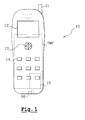
- the figure 1 shows such a radiocommunication terminal 10, essentially comprising a reception antenna 11, a screen 12, typically a liquid crystal display screen, a navigation key 13 and a keypad 14.
- the terminal 10 further comprises a battery 15 integrated and a plug 16 for connecting the battery with a battery charger.
- the terminal 10 comprises a printed circuit IMP to accommodate all the circuits of the radio communication terminal including microprocessor chips of different types.
- the screen of LCD screen type is managed by a microprocessor made on a chip called the GSM chip, which can display on the screen the field bars, the state of the battery etc ..., and allows possible to spin games.
- the GSM chip a microprocessor made on a chip
- Multimedia Support Chips MMCC Multimedia Companion Chip
- Such components have very strong signal processing capabilities to enable the management of multimedia applications such as audio or video for example.
- the auxiliary chips requiring increased display performance, they are directly connected to a screen and it is these components that manage access to the screen.
- the multimedia auxiliary chip must drive the control module of the liquid crystal display screen of the GSM radiocommunication terminal. To do this, such components therefore generally have an internal RAM corresponding to the image of the screen and allowing them to implement their image processing.
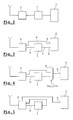
- the figure 2 shows such an architecture where a multimedia auxiliary chip 1 is connected to a GSM chip 2 via a serial link, the GSM chip 2 being provided to manage the conventional functions related to the GSM protocol.
- a parallel bus link is provided to ensure the transfer of information between the multimedia auxiliary chip 1 and a control module 3 which manages the liquid crystal display screen of the mobile radio terminal.
- the standby mode is characterized by a simple listening network, the terminal emitting nothing.
- the liquid crystal display screen must be regularly refreshed with information concerning in particular the state of the network, the state of the battery, etc.
- the GSM standard it is stipulated that a listening of the network must be carried out every 2.5 seconds on average.
- the GSM chip has potentially information to be transmitted to the multimedia auxiliary chip every 2.5 seconds.
- the multimedia auxiliary chip must then exit the standby state to implement the refresh operation of the LCD display screen. In all other cases, modes of de-energizing the auxiliary chip are implemented. The auxiliary chip then deactivates all its unnecessary resources and remains in standby mode.
- FIG. figure 2 Compared to an architecture of a conventional mobile radio terminal where the GSM chip directly controls the liquid crystal display screen via its control module, the architecture illustrated in FIG. figure 2 a "smart" mobile radio terminal where a multimedia auxiliary chip is integrated therefore requires to turn on the multimedia auxiliary chip even when the terminal is in standby mode to refresh the LCD display screen.
- a mobile radio terminal architecture as shown in FIG. figure 2 where the multimedia auxiliary chip controls the control module of the LCD display thus has low performance in terms of power consumption in the standby mode of the terminal.
- the invention provides to avoid using the multimedia auxiliary chip when the radiocommunication terminal is in standby mode.
- the invention provides for deactivating the multimedia auxiliary chip and the liquid crystal display screen is then refreshed directly. via the GSM chip.
- the invention thus relates to a radiocommunication terminal comprising a screen managed by a control module and at least two different types of microprocessor, said first type of microprocessor improves the graphical functionalities of said terminal and controls said control module of the screen, said second type of microprocessor manages the other functionalities of said terminal, which terminal is characterized in that during the duration of the standby mode, said first type of microprocessor is deactivated while said second type of microprocessor controls the control module of the screen.
- the figure 3 shows a first type of microprocessor 1 realized on a chip called multimedia auxiliary chip.
- the auxiliary chip 1 is dedicated specifically to the processing of the multimedia functionalities of the terminal in which it is integrated, thus making it possible to greatly improve the graphical functionalities of the terminal.
- a second type of microprocessor 2 is made on another chip called GSM chip.
- the GSM chip 2 is in fact intended to process the other functionalities of the radio terminal in which it is integrated and in particular the functions related to the management of the GSM protocol.
- the figure 3 finally shows a control module 3 of the liquid crystal display screen having both a serial interface 4 and a parallel interface 5.
- the two types of microprocessor 1 and 2 are each connected to the control module 3 of the liquid crystal display screen.
- the GSM chip 2 having the least information to be transmitted is connected to the serial interface of the control module 3 via a serial bus link 6, while the multimedia auxiliary chip 1 is connected to the parallel interface. of the control module 3 via a parallel bus link 7, the GSM chip 2 and the multimedia auxiliary chip 1 being also connected together via a data transmission line 8.
- a parallel bus link 7 the GSM chip 2 and the multimedia auxiliary chip 1 being also connected together via a data transmission line 8.
- the control module of the liquid crystal display screen is controlled by the multimedia auxiliary chip 1, the GSM chip being as for it planned to manage the other functionalities of the terminal.
- the information concerning, in particular, the display of the field bars, the state of the battery, etc., which are conventionally processed by the GSM chip 2 are then transferred to the auxiliary chip 1 via the data transmission line. 8 so that the auxiliary chip 1 controls the display of this information on the screen.
- the GSM chip 2 becomes the sole master of the control module 3 of the screen via the serial bus link 6.
- the GSM chip 2 that works.
- an information transfer must be performed before deactivating the multimedia auxiliary chip 1, from the auxiliary chip 1 to the GSM chip 2 via the data transmission line 8, so that the GSM chip retrieves the context in which the screen of the terminal was before it takes control and in turn controls the control module of the screen.
- the multimedia auxiliary chip and its memories can therefore be disabled in standby mode, thus allowing better performance in terms of energy saving.
- a deactivation mechanism is therefore implemented to share the control module of the LCD screen between the GSM chip, when the terminal is in standby mode, and the multimedia auxiliary chip in all other cases, which increases the standby time of the terminal or at least make it equivalent to that of a standard radio terminal not implementing a multimedia auxiliary chip.
- liquid crystal display control modules have two types of interface, serial and parallel, as with reference to the figure 1 , but for the most part only a parallel interface.
- the figure 4 proposes then a particular embodiment of the invention capable of adapting to such screen control modules.
- the control module 3 of the liquid crystal display screen of the figure 4 therefore has a single parallel interface 5, which implies that only one circuit can be connected to it.
- the architecture of the figure 4 then additionally comprises an external multiplexer 2x1 9 whose two inputs are respectively connected, one to the first type of microprocessor made on the multimedia auxiliary chip 1, the other to the second type of microprocessor made on the GSM chip 2, by the intermediate of parallel bus type links.
- the output of the multiplexer 9 is connected to the parallel interface of the control module 3 of the liquid crystal display screen via a parallel bus type link.
- the GSM chip 2 and the auxiliary chip 1 are interconnected by the data transmission line 8.
- the role of the multiplexer 9 is to manage an access priority to the control module 3 of the screen between the multimedia auxiliary chip 1 and the GSM chip 2.
- the multiplexer 9 makes it possible to take into account either the data stream that comes from the GSM chip when the terminal is in standby mode, ie the data stream that comes from the multimedia auxiliary chip in other cases.
- the external multiplexer 9 is controlled by a cde-standby command, which can for example be driven by the GSM chip.
- a cde-standby command which can for example be driven by the GSM chip.
- the cde-veille command is applied to the multiplexer 9 via the GSM chip and the data stream taken into account.
- account for controlling the control module of the screen is the one from the GSM chip 2.
- the GSM chip 2 controls the control module 3 of the screen while the multimedia auxiliary chip 1 is deactivated, which allows optimize the power consumption of the terminal in standby mode.
- the auxiliary chip 1 transfers information to the GSM chip 2 via the line 8 so that the GSM chip 2 recovers the context in which the screen was located before it took the hand to control the screen in turn.
- the cde-veille command is not applied to the multiplexer 9 and the data stream taken into account. by the multiplexer will be the one from the multimedia auxiliary chip 1 which will then drive the control module 3 of the screen.
- the auxiliary chip 1 is activated, data is transmitted on the line 8 of the GSM chip 2 to the auxiliary chip 1 which now controls the screen so as to take into account the information conventionally processed by the GSM chip concerning the field bars , the state of the battery etc ...
- the embodiment of the figure 5 illustrates a variant of the embodiment which has just been described with reference to the figure 4 .
- an evolution of the conventional GSM chip is implemented in order to use the minimum component.
- the multiplexer 9 of the figure 4 is advantageously integrated with the GSM chip 2, which must then include additional inputs / outputs. Nevertheless, the connections between the different components remain identical with respect to the figure 4 .
- the integration of the multiplexer 9 with the GSM chip 2 therefore does not modify the operation as it has been described with reference to the figure 4 but allows on the other hand to further optimize the architecture of the figure 4 in terms of cost and space, in addition to allowing an optimization of the autonomy of the terminal in standby mode.
Landscapes
- Engineering & Computer Science (AREA)
- Computer Networks & Wireless Communication (AREA)
- Signal Processing (AREA)
- Telephone Function (AREA)
- Mobile Radio Communication Systems (AREA)
- Transceivers (AREA)
- Two-Way Televisions, Distribution Of Moving Picture Or The Like (AREA)
- Power Sources (AREA)
- Controls And Circuits For Display Device (AREA)
Abstract
Description
- La présente invention se rapporte à un terminal de radiocommunication où la consommation d'une puce auxiliaire multimédia intégrée au terminal est optimisée de sorte à augmenter l'autonomie du terminal en mode veille.
- L'invention se rapporte donc plus particulièrement au domaine des télécommunications et notamment au domaine des terminaux de radiocommunication de type GSM (acronyme pour l'expression anglo-saxonne « Global System Mobil ») susceptibles de mettre en oeuvre des fonctions de type multimédia.
- La
figure 1 montre un tel terminal de radiocommunication 10, comprenant essentiellement une antenne de réception 11, un écran 12, typiquement un écran à affichage par cristaux liquides, une touche de navigation 13 et un pavé de touches 14. Le terminal 10 comprend en plus une batterie 15 intégrée et une fiche de connexion 16 pour la connexion de la batterie avec un chargeur de batterie. Enfin, le terminal 10 comprend un circuit imprimé IMP pour accueillir l'ensemble des circuits du terminal de radiocommunication parmi lesquels des puces de microprocesseur de différents types. - En effet, dans une architecture classique de terminaux de radiocommunication de type GSM, l'écran de type écran à affichage par cristaux liquides est géré par un microprocesseur réalisé sur une puce appelée la puce GSM, qui permet d'afficher à l'écran les barres de champs, l'état de la batterie etc..., et permet éventuellement de faire tourner des jeux. De plus, pour mettre en oeuvre des fonctions de type multimédia par l'intermédiaire de terminaux de radiocommunication GSM, il existe des composants spécifiques appelés puces auxiliaires multimédia MMCC (pour « Multimédia Companion Chip »). De tels composants sont dotés de très fortes capacités de traitement du signal pour permettre la gestion d'applications multimédia de type audio ou vidéo par exemple.
- Le problème technique qui se pose alors concerne la gestion de l'écran à affichage par cristaux liquides lorsqu'une puce auxiliaire multimédia MMCC est intégrée à une architecture classique de terminaux GSM. En effet, on a alors deux microprocesseurs qui doivent cohabiter pour traiter les informations liées à la gestion de l'écran.
- Or, les puces auxiliaires nécessitant des performances d'affichage accrues, elles sont directement connectées à un écran et ce sont donc ces composants qui gèrent les accès à l'écran. Ainsi est-il communément admis que la puce auxiliaire multimédia doit piloter le module de commande de l'écran à affichage par cristaux liquides du terminal de radiocommunication GSM. Pour ce faire, de tels composants possèdent donc généralement une RAM interne correspondant à l'image de l'écran et leur permettant de mettre en oeuvre leur traitement d'image.
- La
figure 2 montre une telle architecture où une puce auxiliaire multimédia 1 est connectée à une puce GSM 2 par l'intermédiaire d'une liaison série, la puce GSM 2 étant prévue pour gérer les fonctionnalités classiques liées au protocole GSM. Une liaison bus parallèle est prévue pour assurer le transfert d'informations entre la puce auxiliaire multimédia 1 et un module de commande 3 qui gère l'écran à affichage par cristaux liquides du terminal de radiocommunication mobile. - On sait que l'économie d'énergie est un enjeu crucial pour les fabricants de terminaux de radiocommunication GSM et cet enjeu se traduit notamment par un souci d'optimiser au mieux l'autonomie en mode veille des terminaux de radiocommunication, le mode veille se caractérisant par une simple écoute du réseau, le terminal n'émettant rien. Cependant, quand le terminal de radiocommunication mobile est en mode veille, l'écran à affichage par cristaux liquides doit être rafraîchi régulièrement avec des informations concernant notamment l'état du réseau, l'état de la batterie, etc...
- Or, on a vu que l'intégration d'une puce auxiliaire multimédia dans un terminal de radiocommunication GSM aboutit à l'architecture de la
figure 2 , où le module de commande de l'écran est piloté par la puce auxiliaire multimédia. - Selon la norme GSM, il est stipulé qu'une écoute du réseau doit être réalisée toutes les 2,5 secondes en moyenne. Ainsi, lorsque le terminal de radiocommunication est en mode veille, la puce GSM a potentiellement des informations à transmettre à la puce auxiliaire multimédia toutes les 2,5 secondes.
- La puce auxiliaire multimédia doit alors sortir de l'état de veille pour mettre en oeuvre l'opération de rafraîchissement de l'écran à affichage par cristaux liquides. Dans tous les autres cas, des modes de mise hors tension de la puce auxiliaire sont mis en oeuvre. La puce auxiliaire désactive alors toutes ses ressources non nécessaires et reste en mode veille.
- Néanmoins, comparé à une architecture d'un terminal de radiocommunication mobile classique où la puce GSM pilote directement l'écran à affichage par cristaux liquides par l'intermédiaire de son module de commande, l'architecture illustrée à la
figure 2 d'un terminal de radiocommunication mobile « intelligent » où une puce auxiliaire multimédia est intégrée impose donc de mettre sous tension la puce auxiliaire multimédia même quand le terminal est en mode veille pour rafraîchir l'écran à affichage par cristaux liquides. - Ainsi, le fait de mettre sous tension la puce auxiliaire multimédia avec ses mémoires pour permettre l'affichage à l'écran d'informations qui concernent l'état du réseau alors que la puce auxiliaire est spécifiquement prévue pour traiter des informations de type multimédia a pour conséquence d'augmenter notablement la consommation d'énergie (notamment à cause des courants de fuite) pendant la durée du mode veille où des opérations de rafraîchissement de l'écran doivent être mises en oeuvre.
- Une architecture de terminal de radiocommunication mobile telle qu'elle est représentée à la
figure 2 où la puce auxiliaire multimédia pilote le module de commande de l'écran à affichage par cristaux liquides présente donc de faibles performances en terme de consommation d'énergie en mode veille du terminal. - C'est par conséquent un objet de la présente invention de pallier aux inconvénients de l'art antérieur sus-mentionnés en proposant une amélioration à l'architecture décrite à la
figure 2 , de sorte à fournir un terminal de radiocommunication type GSM intelligent, c'est à dire intégrant une puce auxiliaire multimédia, doté de performances de consommation d'énergie en mode veille équivalentes à celles d'un terminal de radiocommunication mobile standard. - A cet effet, l'invention prévoit d'éviter d'utiliser la puce auxiliaire multimédia lorsque le terminal de radiocommunication est en mode veille. Ainsi, en mode veille où le terminal n'est pas en communication et met simplement en oeuvre une fonction d'écoute du réseau, l'invention prévoit de désactiver la puce auxiliaire multimédia et l'écran à affichage par cristaux liquides est alors rafraîchi directement par l'intermédiaire de la puce GSM.
- L'invention concerne donc un terminal de radiocommunication comprenant un écran géré par un module de commande et au moins deux types différents de microprocesseur, ledit premier type de microprocesseur améliore les fonctionnalités graphiques dudit terminal et pilote ledit module de commande de l'écran, ledit second type de microprocesseur gère les autres fonctionnalités dudit terminal, lequel terminal est caractérisé en ce que pendant la durée du mode veille, ledit premier type de microprocesseur est désactivé tandis que ledit second type de microprocesseur pilote le module de commande de l'écran.
- D'autres caractéristiques et avantages de la présente invention apparaîtront plus clairement à la lecture de la description qui suit donnée à titre d'exemple illustratif et non limitatif et faite en référence aux figures annexées dans lesquelles :
- la
figure 1 est un schéma illustrant un terminal de radiocommunication standard et a déjà été décrite ; - la
figure 2 est un schéma illustrant les inconvénients liés à l'intégration d'une puce auxiliaire multimédia dans une architecture de terminal de radiocommunication standard et a déjà été décrite ; - la
figure 3 est un schéma illustrant un premier mode de réalisation de l'invention ; - la
figure 4 est un schéma illustrant un second mode de réalisation de l'invention, et - la
figure 5 est un schéma illustrant un troisième mode de réalisation de l'invention. - On retrouve aux
figures 3, 4 et 5 les mêmes éléments que ceux déjà décrits en référence à lafigure 2 . Ainsi, lafigure 3 montre un premier type de microprocesseur 1 réalisé sur une puce appelée puce auxiliaire multimédia. La puce auxiliaire 1 est dédiée spécifiquement au traitement des fonctionnalités multimédia du terminal dans lequel elle est intégrée, permettant ainsi d'améliorer fortement les fonctionnalités graphiques du terminal. - Un deuxième type de microprocesseur 2 est réalisé sur une autre puce appelée puce GSM. La puce GSM 2 est en effet prévue pour traiter les autres fonctionnalités du terminal de radiocommunication dans lequel elle est intégrée et en particulier les fonctionnalités liées à la gestion du protocole GSM.
- La
figure 3 montre enfin un module de commande 3 de l'écran à affichage par cristaux liquides disposant à la fois d'une interface série 4 et d'une interface parallèle 5. Dans ce premier mode de réalisation de l'invention, les deux types de microprocesseur 1 et 2 sont chacun connectés au module de commande 3 de l'écran à affichage par cristaux liquides. La puce GSM 2 ayant le moins d'informations à transmettre est connectée à l'interface série du module de commande 3 par l'intermédiaire d'une liaison bus série 6, tandis que la puce auxiliaire multimédia 1 est connectée à l'interface parallèle du module de commande 3 par l'intermédiaire d'une liaison bus parallèle 7, la puce GSM 2 et la puce auxiliaire multimédia 1 étant également connectées ensemble par l'intermédiaire d'une ligne de transmission de données 8. A un instant donné, on considère qu'il n'y a qu'un seul type de microprocesseur maître du module de commande de l'écran à affichage par cristaux liquides. - Dans cette configuration, notamment pour les applications de type multimédia, le module de commande de l'écran à affichage par cristaux liquides est piloté par la puce auxiliaire multimédia 1, la puce GSM étant quant à elle prévue pour gérer les autres fonctionnalités du terminal. Les informations concernant notamment l'affichage des barres de champ, l'état de la batterie etc... qui sont classiquement traitées par la puce GSM 2 sont alors transférées vers la puce auxiliaire 1 par l'intermédiaire de la ligne de transmission de données 8 de sorte à ce que la puce auxiliaire 1 commande l'affichage de ces informations à l'écran.
- Cependant, lorsque le terminal passe en mode veille, c'est à dire qu'il est simplement en écoute du réseau, l'utilisateur ayant décidé d'arrêter les applications multimédia en cours, la puce GSM 2 devient seule maître du module de commande 3 de l'écran par l'intermédiaire le la liaison bus série 6. Ainsi, en mode veille, il n'y a que la puce GSM 2 qui travaille. Auquel cas, un transfert d'informations doit être réalisé avant de désactiver la puce auxiliaire multimédia 1, de la puce auxiliaire 1 vers la puce GSM 2 par l'intermédiaire de la ligne de transmission de données 8, de sorte que la puce GSM récupère le contexte dans lequel se trouvait l'écran du terminal avant qu'elle ne prenne la main et pilote à son tour le module de commande de l'écran.
- La puce auxiliaire multimédia ainsi que ses mémoires, peut donc être désactivée en mode veille, autorisant ainsi de meilleures performances en terme d'économie d'énergie. Un mécanisme de désactivation est donc mis en oeuvre pour partager le module de commande de l'écran à affichage par cristaux liquides entre la puce GSM, lorsque le terminal est en mode veille, et la puce auxiliaire multimédia dans tous les autres cas, ce qui permet d'augmenter l'autonomie en veille du terminal ou du moins de la rendre équivalente à celle d'un terminal de radiocommunication standard ne mettant pas en oeuvre de puce auxiliaire multimédia.
- Il est à noter que tous les modules de commande d'écran à affichage par cristaux liquides ne possèdent pas deux types d'interface, série et parallèle, comme en référence à la
figure 1 , mais pour la plupart seulement une interface parallèle. Lafigure 4 propose alors un mode de réalisation particulier de l'invention susceptible de s'adapter à de tels modules de commande d'écran. - Le module de commande 3 de l'écran à affichage par cristaux liquides de la
figure 4 possède donc une seule interface parallèle 5, ce qui implique qu'un seul circuit peut lui être connecté. - L'architecture de la
figure 4 comprend alors en plus un multiplexeur externe 2x1 9 dont les deux entrées sont connectées respectivement, l'une au premier type de microprocesseur réalisée sur la puce auxiliaire multimédia 1, l'autre au deuxième type de microprocesseur réalisé sur la puce GSM 2, par l'intermédiaire de liaisons de type bus parallèle. La sortie du multiplexeur 9 est quant à elle connectée à l'interface parallèle du module de commande 3 de l'écran à affichage par cristaux liquides par l'intermédiaire d'une liaison de type bus parallèle. Enfin, la puce GSM 2 et la puce auxiliaire 1 sont reliées entre elles par la ligne de transmission de données 8. - Le rôle du multiplexeur 9 est de gérer une priorité d'accès au module de commande 3 de l'écran entre la puce auxiliaire multimédia 1 et la puce GSM 2. Le multiplexeur 9 permet de prendre en compte soit le flux de données qui vient de la puce GSM lorsque le terminal est en mode veille, soit le flux de données qui vient de la puce auxiliaire multimédia dans les autres cas.
- Pour ce faire, le multiplexeur externe 9 est commandée par une commande cde-veille, laquelle peut par exemple être pilotée par la puce GSM. Ainsi, lorsque le terminal se trouve en mode veille et que l'utilisateur décide d'arrêter les applications multimédia en cours, la commande cde-veille est appliquée au multiplexeur 9 par l'intermédiaire de la puce GSM et le flux de données pris en compte pour piloter le module de commande de l'écran est celui issu de la puce GSM 2. La puce GSM 2 pilote alors le module de commande 3 de l'écran tandis que la puce auxiliaire multimédia 1 est désactivée, ce qui permet d'optimiser la consommation d'énergie du terminal en mode veille. Préalablement à sa désactivation, la puce auxiliaire 1 transfère des informations à la puce GSM 2 par l'intermédiaire de la ligne 8 de sorte que la puce GSM 2 récupère le contexte dans lequel se trouvait l'écran avant qu'elle ne prenne la main pour piloter à son tour l'écran.
- Inversement, lorsque le terminal n'est plus en mode veille ou que l'utilisateur lance des applications multimédia, la commande cde-veille n'est pas appliquée au multiplexeur 9 et le flux de données pris en compte par le multiplexeur sera celui issu de la puce auxiliaire multimédia 1 qui va alors piloter le module de commande 3 de l'écran. Quand la puce auxiliaire 1 est activée, des données sont transmises sur la ligne 8 de la puce GSM 2 vers la puce auxiliaire 1 qui pilote dorénavant l'écran de façon à tenir compte des informations classiquement traitées par la puce GSM concernant les barres de champs, l'état de la batterie etc...
- Enfin, le mode de réalisation de la
figure 5 illustre une variante du mode de réalisation qui vient d'être décrit en référence à lafigure 4 . Dans cette variante, une évolution de la puce GSM classique est mise en oeuvre dans un souci d'utiliser le minimum de composant. Ainsi, le multiplexeur 9 de lafigure 4 est avantageusement intégré à la puce GSM 2, laquelle doit alors comprendre des entrées/sorties supplémentaires. Néanmoins, les connexions entre les différents composants restent identiques par rapport à lafigure 4 . L'intégration du multiplexeur 9 à la puce GSM 2 ne modifie donc en rien le fonctionnement tel qu'il a été décrit en référence à lafigure 4 mais permet par contre d'optimiser davantage l'architecture de lafigure 4 en terme de coût et de place, en plus de permettre une optimisation de l'autonomie du terminal en mode veille. - La présente invention inclut également les modes de réalisation préférés suivants:
- 1. Terminal de radiocommunication (10) comprenant un écran (12) géré par un module de commande (3) et au moins deux types différents de microprocesseur (1,2), ledit premier type de microprocesseur (1) améliore les fonctionnalités graphiques dudit terminal (10) et pilote ledit module de commande (3) de l'écran (12), ledit second type de microprocesseur (2) gère les autres fonctionnalités dudit terminal (10) caractérisé en ce que pendant le mode veille, ledit premier type de microprocesseur (1) est désactivé tandis que ledit second type de microprocesseur (2) pilote ledit module de commande (3) de l'écran (12).
- 2. Terminal de radiocommunication (10) selon le mode de réalisation 1, caractérisé en ce que le module de commande (3) de l'écran (12) comprend une interface parallèle (5) et une interface série (4), ladite interface parallèle étant connectée au premier type de microprocesseur (1) par l'intermédiaire d'une liaison bus parallèle (7), ladite interface série (4) étant connectée au deuxième type de microprocesseur (2) par l'intermédiaire d'une liaison bus série (6), et lesdits premier (1) et deuxième (2) type de microprocesseur étant connectés ensemble par l'intermédiaire d'une ligne de transmission de données (8).
- 3. Terminal de radiocommunication (10) selon le mode de réalisation 1, caractérisé en ce que le module de commande (3) de l'écran (12) comprend une unique interface parallèle (5), ledit terminal (10) comprenant en plus un multiplexeur externe (9) dont une sortie est connectée par une liaison bus parallèle à ladite interface parallèle (5) dudit module de commande (3) de l'écran (12) et dont une première et une deuxième entrée sont connectées respectivement au premier (1) et au deuxième (2) type de microprocesseur par l'intermédiaire de liaisons bus parallèle, lesdits premier (1) et deuxième (2) type de microprocesseur étant connectés l'un à l'autre par l'intermédiaire d'une ligne de transmission de données (8).
- 4. Terminal de radiocommunication (10) selon le mode de réalisation 3, caractérisé en ce que le multiplexeur (9) est intégré à la puce sur laquelle est réalisé le deuxième type de microprocesseur.
- 5. Terminal de radiocommunication (10) selon le mode de réalisation 3 ou 4, caractérisé en ce que le multiplexeur (9) est commandée par l'application d'une commande (cde-veille) pilotée par le deuxième type de microprocesseur (2) de façon à permettre audit multiplexeur (9) de gérer une priorité d'accès au module de commande (3) de l'écran entre lesdits premier (1) et deuxième (2) microprocesseurs suivant que ledit terminal (10) est en mode veille ou non.
- 6. Terminal de radiocommunication (10) selon l'un des modes de réalisation précédentes, caractérisé en ce que le premier type de microprocesseur (1) est dédié au traitement des fonctionnalités multimédia dudit terminal (10).
- 7. Terminal de radiocommunication (10) selon l'un des modes de réalisation précédentes, caractérisé en ce que le deuxième type de microprocesseur (2) est dédié au traitement des fonctionnalités liées au protocole GSM.
Claims (15)
- Terminal de radiocommunication (10) comprenant un écran (12), un module de commande (3) configuré pour commander l'écran (12), un premier microprocesseur (1) configuré pour piloter le module de commande (3) pour gérer des fonctionnalités multimédia de l'écran (12) et un second microprocesseur (2) configuré pour piloter le module de commande (3) pour gérer des fonctionnalités autres que les fonctionnalités multimédia de l'écran (12), caractérisé en ce que le second microprocesseur (2) est configuré pour piloter le module de commande (3) indépendamment du premier microprocesseur (1).
- Terminal de radiocommunication (10) selon la revendication 1, caractérisé en ce que le second microprocesseur (2) est en outre configuré pour piloter le module de commande (3) par l'intermédiaire du premier microprocesseur (1).
- Terminal de radiocommunication (10) selon la revendication 2, caractérisé en ce que le second microprocesseur (2) est configuré pour piloter le module de commande (3) indépendamment du premier microprocesseur (1) lorsque le terminal de radiocommunication (10) est dans un mode veille et par l'intermédiaire du premier microprocesseur (1) lorsque le terminal de radiocommunication (10) n'est pas en mode veille.
- Terminal de radiocommunication (10) selon la revendication 1, caractérisé en ce que le second microprocesseur (2) est réalisé sur une puce de système global de télécommunication avec les mobiles (GSM).
- Terminal de radiocommunication (10) selon la revendication 1, caractérisé en ce que le premier microprocesseur (1) est réalisé sur une puce auxiliaire multimédia.
- Terminal de radiocommunication (10) selon la revendication 1, caractérisé en ce que le second microprocesseur (2) est configuré pour réaliser des fonctionnalités qui sont liées à la gestion d'un protocole GSM.
- Terminal de radiocommunication (10) selon la revendication 1, caractérisé en ce que le second microprocesseur (2) est connecté au module de commande (3) par l'intermédiaire d'une liaison bus série (6) ou d'une ligne de transmission de données (8).
- Terminal de radiocommunication (10) selon la revendication 1, caractérisé en ce que le premier microprocesseur (1) est connecté au module de commande (3) par l'intermédiaire d'une interface parallèle (5).
- Terminal de radiocommunication (10) selon la revendication 1, caractérisé en ce que uniquement l'un des premier (1) et second (2) microprocesseurs est configuré pour piloter le module de commande (3) à un instant donné.
- Terminal de radiocommunication (10) selon la revendication 1, caractérisé en ce que lorsque le terminal de radiocommunication (10) est en mode veille, le second microprocesseur (2) est configuré pour désactiver le premier microprocesseur (1).
- Terminal de radiocommunication (10) selon la revendication 1, caractérisé en ce que les premier (1) et second (2) microprocesseurs sont connectés au module de commande (3) par l'intermédiaire d'un multiplexeur (9).
- Terminal de radiocommunication (10) selon la revendication 11, caractérisé en ce que le multiplexeur (9) est connecté à une interface parallèle (5) du module de commande (3).
- Terminal de radiocommunication (10) selon la revendication 11, caractérisé en ce que le multiplexeur (9) est commandé par une commande, de telle sorte que lorsque le terminal de radiocommunication (10) est en mode veille, la commande est appliquée au multiplexeur (9) de telle sorte que le second microprocesseur (2) transfère des informations au module de commande (3).
- Terminal de radiocommunication (10) selon la revendication 11, caractérisé en ce que le multiplexeur (9) est commandé par une commande, de telle sorte que lorsque le terminal de radiocommunication (10) n'est pas en mode veille, la commande n'est pas appliquée au multiplexeur (9) de telle sorte que le premier microprocesseur (1) transfère des informations au module de commande (3).
- Terminal de radiocommunication (10) selon la revendication 11, caractérisé en ce que le second microprocesseur (2) est réalisé sur une puce GSM et le multiplexeur (9) est intégré à la puce GSM.
Applications Claiming Priority (2)
| Application Number | Priority Date | Filing Date | Title |
|---|---|---|---|
| FR0115776A FR2833448B1 (fr) | 2001-12-06 | 2001-12-06 | Optimisation de la consommation d'une puce auxiliaire multimedia dans un terminal de la radiocommunication mobile |
| EP02293001A EP1322127B1 (fr) | 2001-12-06 | 2002-12-05 | Optimisation de la consommation d'une puce auxiliaire multimedia dans un terminal de radiocommunication mobile |
Related Parent Applications (2)
| Application Number | Title | Priority Date | Filing Date |
|---|---|---|---|
| EP02293001A Division EP1322127B1 (fr) | 2001-12-06 | 2002-12-05 | Optimisation de la consommation d'une puce auxiliaire multimedia dans un terminal de radiocommunication mobile |
| EP02293001.0 Division | 2002-12-05 |
Publications (3)
| Publication Number | Publication Date |
|---|---|
| EP2149836A2 true EP2149836A2 (fr) | 2010-02-03 |
| EP2149836A3 EP2149836A3 (fr) | 2011-04-13 |
| EP2149836B1 EP2149836B1 (fr) | 2018-08-01 |
Family
ID=8870176
Family Applications (2)
| Application Number | Title | Priority Date | Filing Date |
|---|---|---|---|
| EP09172808.9A Expired - Lifetime EP2149836B1 (fr) | 2001-12-06 | 2002-12-05 | Optimisation de la consommation d'une puce auxiliaire multimedia dans un terminal de radiocommunication mobile |
| EP02293001A Expired - Lifetime EP1322127B1 (fr) | 2001-12-06 | 2002-12-05 | Optimisation de la consommation d'une puce auxiliaire multimedia dans un terminal de radiocommunication mobile |
Family Applications After (1)
| Application Number | Title | Priority Date | Filing Date |
|---|---|---|---|
| EP02293001A Expired - Lifetime EP1322127B1 (fr) | 2001-12-06 | 2002-12-05 | Optimisation de la consommation d'une puce auxiliaire multimedia dans un terminal de radiocommunication mobile |
Country Status (9)
| Country | Link |
|---|---|
| US (1) | US7058427B2 (fr) |
| EP (2) | EP2149836B1 (fr) |
| JP (1) | JP4458399B2 (fr) |
| CN (1) | CN100488320C (fr) |
| AT (1) | ATE449517T1 (fr) |
| DE (1) | DE60234416D1 (fr) |
| DK (1) | DK1322127T3 (fr) |
| ES (1) | ES2336311T3 (fr) |
| FR (1) | FR2833448B1 (fr) |
Families Citing this family (22)
| Publication number | Priority date | Publication date | Assignee | Title |
|---|---|---|---|---|
| KR100498941B1 (ko) * | 2003-02-04 | 2005-07-04 | 삼성전자주식회사 | 외부 표시부를 제어하기 위한 복합휴대단말장치 및 그 방법 |
| DE10340424B4 (de) * | 2003-09-02 | 2006-07-27 | Infineon Technologies Ag | Betriebszustandsabhängige Verteilung von Aufgaben in Mobilkommunikations-Endgeräten mit mehreren Mikro-Prozessoren |
| JP4677730B2 (ja) * | 2004-03-26 | 2011-04-27 | 日本電気株式会社 | 携帯端末装置、制御方法およびそのプログラム |
| KR100677327B1 (ko) * | 2004-06-16 | 2007-02-02 | 엘지전자 주식회사 | 이중 운영체제를 가진 이동통신 단말기 |
| US7444192B2 (en) | 2004-10-26 | 2008-10-28 | Aerovironment, Inc. | Reactive replenishable device management |
| KR100724961B1 (ko) * | 2006-07-28 | 2007-06-04 | 삼성전자주식회사 | 멀티미디어 기능을 구비한 휴대 단말기의 동작 제어 장치및 방법 |
| CN101552819A (zh) * | 2009-03-30 | 2009-10-07 | 李林冲 | 单向待机手机 |
| CN103440031A (zh) * | 2013-09-11 | 2013-12-11 | 广州市久邦数码科技有限公司 | 一种移动终端关屏自动优化的省电系统及方法 |
| US11874716B2 (en) | 2015-08-05 | 2024-01-16 | Suunto Oy | Embedded computing device management |
| CN105100507A (zh) * | 2015-09-28 | 2015-11-25 | 深圳市亿通科技有限公司 | 一种移动终端任务处理方法及系统 |
| US11210299B2 (en) | 2015-12-01 | 2021-12-28 | Amer Sports Digital Services Oy | Apparatus and method for presenting thematic maps |
| US11144107B2 (en) | 2015-12-01 | 2021-10-12 | Amer Sports Digital Services Oy | Apparatus and method for presenting thematic maps |
| US11215457B2 (en) | 2015-12-01 | 2022-01-04 | Amer Sports Digital Services Oy | Thematic map based route optimization |
| US11137820B2 (en) | 2015-12-01 | 2021-10-05 | Amer Sports Digital Services Oy | Apparatus and method for presenting thematic maps |
| DE102016015695A1 (de) | 2015-12-21 | 2017-06-22 | Suunto Oy | Aktivitätsintensitätspegel-Bestimmung |
| GB2545668B (en) | 2015-12-21 | 2020-05-20 | Suunto Oy | Sensor based context management |
| US11541280B2 (en) | 2015-12-21 | 2023-01-03 | Suunto Oy | Apparatus and exercising device |
| US11284807B2 (en) | 2015-12-21 | 2022-03-29 | Amer Sports Digital Services Oy | Engaging exercising devices with a mobile device |
| US11587484B2 (en) | 2015-12-21 | 2023-02-21 | Suunto Oy | Method for controlling a display |
| US11838990B2 (en) | 2015-12-21 | 2023-12-05 | Suunto Oy | Communicating sensor data in wireless communication systems |
| US11703938B2 (en) | 2016-10-17 | 2023-07-18 | Suunto Oy | Embedded computing device |
| DE102017009171B4 (de) | 2016-10-17 | 2025-05-22 | Suunto Oy | Eingebettete rechenvorrichtung |
Citations (1)
| Publication number | Priority date | Publication date | Assignee | Title |
|---|---|---|---|---|
| WO1993025955A1 (fr) | 1992-06-12 | 1993-12-23 | Norand Corporation | Processeur de donnees portable activant et desactivant selectivement des unites modulaires internes et un processeur d'application pour economiser l'energie |
Family Cites Families (9)
| Publication number | Priority date | Publication date | Assignee | Title |
|---|---|---|---|---|
| US4545030A (en) * | 1982-09-28 | 1985-10-01 | The John Hopkins University | Synchronous clock stopper for microprocessor |
| JPH0642691B2 (ja) * | 1988-05-21 | 1994-06-01 | 富士通株式会社 | 移動電話端末 |
| US5142684A (en) * | 1989-06-23 | 1992-08-25 | Hand Held Products, Inc. | Power conservation in microprocessor controlled devices |
| GB2289146B (en) * | 1994-04-12 | 1998-09-09 | Nokia Mobile Phones Ltd | Buffering data |
| US6040845A (en) * | 1997-12-22 | 2000-03-21 | Compaq Computer Corp. | Device and method for reducing power consumption within an accelerated graphics port target |
| EP1077442A1 (fr) * | 1999-08-17 | 2001-02-21 | Koninklijke Philips Electronics N.V. | Ecran doté d'une zone d'affichage à geométrie variable |
| JP4183222B2 (ja) * | 2000-06-02 | 2008-11-19 | 日本電気株式会社 | 携帯電話機の省電力駆動方法 |
| US20020173344A1 (en) * | 2001-03-16 | 2002-11-21 | Cupps Bryan T. | Novel personal electronics device |
| JP2003274010A (ja) * | 2002-03-14 | 2003-09-26 | Hitachi Ltd | 携帯電話機 |
-
2001
- 2001-12-06 FR FR0115776A patent/FR2833448B1/fr not_active Expired - Fee Related
-
2002
- 2002-12-03 US US10/308,014 patent/US7058427B2/en not_active Expired - Lifetime
- 2002-12-04 JP JP2002352591A patent/JP4458399B2/ja not_active Expired - Fee Related
- 2002-12-05 DK DK02293001.0T patent/DK1322127T3/da active
- 2002-12-05 ES ES02293001T patent/ES2336311T3/es not_active Expired - Lifetime
- 2002-12-05 EP EP09172808.9A patent/EP2149836B1/fr not_active Expired - Lifetime
- 2002-12-05 DE DE60234416T patent/DE60234416D1/de not_active Expired - Lifetime
- 2002-12-05 CN CNB021559104A patent/CN100488320C/zh not_active Expired - Fee Related
- 2002-12-05 AT AT02293001T patent/ATE449517T1/de not_active IP Right Cessation
- 2002-12-05 EP EP02293001A patent/EP1322127B1/fr not_active Expired - Lifetime
Patent Citations (1)
| Publication number | Priority date | Publication date | Assignee | Title |
|---|---|---|---|---|
| WO1993025955A1 (fr) | 1992-06-12 | 1993-12-23 | Norand Corporation | Processeur de donnees portable activant et desactivant selectivement des unites modulaires internes et un processeur d'application pour economiser l'energie |
Also Published As
| Publication number | Publication date |
|---|---|
| EP2149836B1 (fr) | 2018-08-01 |
| ES2336311T3 (es) | 2010-04-12 |
| EP2149836A3 (fr) | 2011-04-13 |
| US7058427B2 (en) | 2006-06-06 |
| EP1322127B1 (fr) | 2009-11-18 |
| EP1322127A1 (fr) | 2003-06-25 |
| FR2833448A1 (fr) | 2003-06-13 |
| DE60234416D1 (de) | 2009-12-31 |
| CN100488320C (zh) | 2009-05-13 |
| DK1322127T3 (da) | 2010-01-18 |
| FR2833448B1 (fr) | 2004-02-27 |
| CN1423504A (zh) | 2003-06-11 |
| US20030109287A1 (en) | 2003-06-12 |
| ATE449517T1 (de) | 2009-12-15 |
| JP4458399B2 (ja) | 2010-04-28 |
| JP2003209617A (ja) | 2003-07-25 |
Similar Documents
| Publication | Publication Date | Title |
|---|---|---|
| EP1322127B1 (fr) | Optimisation de la consommation d'une puce auxiliaire multimedia dans un terminal de radiocommunication mobile | |
| KR101422367B1 (ko) | 컴퓨터를 저 전력 보조 프로세서를 통해 운영하기 위한 방법들 및 시스템들 | |
| EP0614303A1 (fr) | Procédé pour délivrer un numéro de téléphone associé à un abonnement téléphonique, postes téléphoniques et téléphone mobile mettant en oeuvre ce procédé | |
| EP0703717A1 (fr) | Economie d'énergie dans un système incluant un radiotéléphone portatif connecté à un dispositif périphérique | |
| EP3258380A1 (fr) | Coeur de processeur asynchrone et microcontrôleur de noeud de capteur communicant comportant un tel coeur de processeur | |
| FR2948785A1 (fr) | Terminateur de transaction | |
| FR3107974A1 (fr) | Procédé et dispositif d’allocation de ressources réseau à un véhicule | |
| CN1326336C (zh) | 包括电源控制功能的光通信盘及具有此盘的系统 | |
| EP1405466A2 (fr) | Systeme de reveil de stations associees pour la mise en oeuvre d'au moins une fonction repartie, notamment dans un vehicule automobile | |
| CA2619301A1 (fr) | Passerelle de communication entre deux entites | |
| EP1065626B1 (fr) | Gestion de la mémoire d'une carte à puce pour les modes d'économie d'énergie dans un téléphone mobile | |
| EP0932112A1 (fr) | Lecteur de carte à puce muni d'un commutateur d'horloge | |
| FR3041782A1 (fr) | Procede de reveil d'un calculateur, notamment pour un systeme de charge de batterie de vehicule hybride | |
| EP0373043A1 (fr) | Système électronique à plusieurs unités amovibles | |
| FR3137512A1 (fr) | Alimentation d'un dispositif électronique | |
| EP4007286A1 (fr) | Procédé de gestion d'une communication entre un dispositif de commande et un terminal de lecture | |
| FR2702578A1 (fr) | Système de communication avec un réseau. | |
| EP0424212B1 (fr) | Radiotéléphone | |
| EP3876096B1 (fr) | Procédé mis en oeuvre dans un module à circuit intégré, module à circuit intégré correspondant, système comportant un tel module et programme d'ordinateur associé | |
| FR2878377A1 (fr) | Connecteur unique pour terminal de communication, circuit electronique, terminal et cable correspondants | |
| EP1175016B1 (fr) | Circuit intégré pouvant fonctionner en des modes actif et inactif et appareil comportant un tel circuit | |
| EP4705871A1 (fr) | Procédé et dispositif de contrôle d'un dispositif d'affichage d'un véhicule via un réseau de type transmission différentielle basse-tension | |
| FR3141305A1 (fr) | Gestion de l’alimentation dans un contrôleur de communication en champ proche - NFC. | |
| EP1363443B1 (fr) | Adapteur universel de téléphone "mains libres" de voiture | |
| EP0945843A1 (fr) | Procédé de contrÔle d'un afficheur à cristaux liquides |
Legal Events
| Date | Code | Title | Description |
|---|---|---|---|
| PUAI | Public reference made under article 153(3) epc to a published international application that has entered the european phase |
Free format text: ORIGINAL CODE: 0009012 |
|
| AC | Divisional application: reference to earlier application |
Ref document number: 1322127 Country of ref document: EP Kind code of ref document: P |
|
| AK | Designated contracting states |
Kind code of ref document: A2 Designated state(s): AT BE BG CH CY CZ DE DK EE ES FI FR GB GR IE IT LI LU MC NL PT SE SI SK TR |
|
| PUAL | Search report despatched |
Free format text: ORIGINAL CODE: 0009013 |
|
| AK | Designated contracting states |
Kind code of ref document: A3 Designated state(s): AT BE BG CH CY CZ DE DK EE ES FI FR GB GR IE IT LI LU MC NL PT SE SI SK TR |
|
| RIC1 | Information provided on ipc code assigned before grant |
Ipc: H04M 1/73 20060101ALI20110308BHEP Ipc: H04W 88/02 20090101ALI20110308BHEP Ipc: H04W 52/02 20090101ALI20110308BHEP Ipc: G06F 1/32 20060101AFI20091228BHEP |
|
| 17P | Request for examination filed |
Effective date: 20111005 |
|
| RAP1 | Party data changed (applicant data changed or rights of an application transferred) |
Owner name: EMERJ, LTD. |
|
| RAP1 | Party data changed (applicant data changed or rights of an application transferred) |
Owner name: Z124 |
|
| 17Q | First examination report despatched |
Effective date: 20120910 |
|
| RAP1 | Party data changed (applicant data changed or rights of an application transferred) |
Owner name: DRNC HOLDINGS, INC. |
|
| REG | Reference to a national code |
Ref country code: DE Ref legal event code: R079 Ref document number: 60249543 Country of ref document: DE Free format text: PREVIOUS MAIN CLASS: G06F0001320000 Ipc: H04W0052020000 |
|
| GRAP | Despatch of communication of intention to grant a patent |
Free format text: ORIGINAL CODE: EPIDOSNIGR1 |
|
| STAA | Information on the status of an ep patent application or granted ep patent |
Free format text: STATUS: GRANT OF PATENT IS INTENDED |
|
| RIC1 | Information provided on ipc code assigned before grant |
Ipc: H04W 88/02 20090101ALI20180131BHEP Ipc: H04W 52/02 20090101AFI20180131BHEP |
|
| INTG | Intention to grant announced |
Effective date: 20180302 |
|
| GRAS | Grant fee paid |
Free format text: ORIGINAL CODE: EPIDOSNIGR3 |
|
| GRAA | (expected) grant |
Free format text: ORIGINAL CODE: 0009210 |
|
| STAA | Information on the status of an ep patent application or granted ep patent |
Free format text: STATUS: THE PATENT HAS BEEN GRANTED |
|
| AC | Divisional application: reference to earlier application |
Ref document number: 1322127 Country of ref document: EP Kind code of ref document: P |
|
| AK | Designated contracting states |
Kind code of ref document: B1 Designated state(s): AT BE BG CH CY CZ DE DK EE ES FI FR GB GR IE IT LI LU MC NL PT SE SI SK TR |
|
| REG | Reference to a national code |
Ref country code: GB Ref legal event code: FG4D Free format text: NOT ENGLISH |
|
| REG | Reference to a national code |
Ref country code: CH Ref legal event code: EP Ref country code: AT Ref legal event code: REF Ref document number: 1025849 Country of ref document: AT Kind code of ref document: T Effective date: 20180815 |
|
| REG | Reference to a national code |
Ref country code: IE Ref legal event code: FG4D Free format text: LANGUAGE OF EP DOCUMENT: FRENCH |
|
| REG | Reference to a national code |
Ref country code: DE Ref legal event code: R096 Ref document number: 60249543 Country of ref document: DE |
|
| REG | Reference to a national code |
Ref country code: NL Ref legal event code: FP |
|
| PGFP | Annual fee paid to national office [announced via postgrant information from national office to epo] |
Ref country code: NL Payment date: 20181123 Year of fee payment: 17 |
|
| REG | Reference to a national code |
Ref country code: AT Ref legal event code: MK05 Ref document number: 1025849 Country of ref document: AT Kind code of ref document: T Effective date: 20180801 |
|
| PG25 | Lapsed in a contracting state [announced via postgrant information from national office to epo] |
Ref country code: FI Free format text: LAPSE BECAUSE OF FAILURE TO SUBMIT A TRANSLATION OF THE DESCRIPTION OR TO PAY THE FEE WITHIN THE PRESCRIBED TIME-LIMIT Effective date: 20180801 Ref country code: GR Free format text: LAPSE BECAUSE OF FAILURE TO SUBMIT A TRANSLATION OF THE DESCRIPTION OR TO PAY THE FEE WITHIN THE PRESCRIBED TIME-LIMIT Effective date: 20181102 Ref country code: AT Free format text: LAPSE BECAUSE OF FAILURE TO SUBMIT A TRANSLATION OF THE DESCRIPTION OR TO PAY THE FEE WITHIN THE PRESCRIBED TIME-LIMIT Effective date: 20180801 Ref country code: SE Free format text: LAPSE BECAUSE OF FAILURE TO SUBMIT A TRANSLATION OF THE DESCRIPTION OR TO PAY THE FEE WITHIN THE PRESCRIBED TIME-LIMIT Effective date: 20180801 Ref country code: BG Free format text: LAPSE BECAUSE OF FAILURE TO SUBMIT A TRANSLATION OF THE DESCRIPTION OR TO PAY THE FEE WITHIN THE PRESCRIBED TIME-LIMIT Effective date: 20181101 |
|
| PGFP | Annual fee paid to national office [announced via postgrant information from national office to epo] |
Ref country code: DE Payment date: 20181126 Year of fee payment: 17 |
|
| PG25 | Lapsed in a contracting state [announced via postgrant information from national office to epo] |
Ref country code: ES Free format text: LAPSE BECAUSE OF FAILURE TO SUBMIT A TRANSLATION OF THE DESCRIPTION OR TO PAY THE FEE WITHIN THE PRESCRIBED TIME-LIMIT Effective date: 20180801 |
|
| PGFP | Annual fee paid to national office [announced via postgrant information from national office to epo] |
Ref country code: FR Payment date: 20181127 Year of fee payment: 17 Ref country code: GB Payment date: 20181127 Year of fee payment: 17 |
|
| PG25 | Lapsed in a contracting state [announced via postgrant information from national office to epo] |
Ref country code: IT Free format text: LAPSE BECAUSE OF FAILURE TO SUBMIT A TRANSLATION OF THE DESCRIPTION OR TO PAY THE FEE WITHIN THE PRESCRIBED TIME-LIMIT Effective date: 20180801 Ref country code: CZ Free format text: LAPSE BECAUSE OF FAILURE TO SUBMIT A TRANSLATION OF THE DESCRIPTION OR TO PAY THE FEE WITHIN THE PRESCRIBED TIME-LIMIT Effective date: 20180801 Ref country code: EE Free format text: LAPSE BECAUSE OF FAILURE TO SUBMIT A TRANSLATION OF THE DESCRIPTION OR TO PAY THE FEE WITHIN THE PRESCRIBED TIME-LIMIT Effective date: 20180801 |
|
| REG | Reference to a national code |
Ref country code: DE Ref legal event code: R097 Ref document number: 60249543 Country of ref document: DE |
|
| PG25 | Lapsed in a contracting state [announced via postgrant information from national office to epo] |
Ref country code: DK Free format text: LAPSE BECAUSE OF FAILURE TO SUBMIT A TRANSLATION OF THE DESCRIPTION OR TO PAY THE FEE WITHIN THE PRESCRIBED TIME-LIMIT Effective date: 20180801 Ref country code: SK Free format text: LAPSE BECAUSE OF FAILURE TO SUBMIT A TRANSLATION OF THE DESCRIPTION OR TO PAY THE FEE WITHIN THE PRESCRIBED TIME-LIMIT Effective date: 20180801 |
|
| PLBE | No opposition filed within time limit |
Free format text: ORIGINAL CODE: 0009261 |
|
| STAA | Information on the status of an ep patent application or granted ep patent |
Free format text: STATUS: NO OPPOSITION FILED WITHIN TIME LIMIT |
|
| 26N | No opposition filed |
Effective date: 20190503 |
|
| REG | Reference to a national code |
Ref country code: CH Ref legal event code: PL |
|
| PG25 | Lapsed in a contracting state [announced via postgrant information from national office to epo] |
Ref country code: SI Free format text: LAPSE BECAUSE OF FAILURE TO SUBMIT A TRANSLATION OF THE DESCRIPTION OR TO PAY THE FEE WITHIN THE PRESCRIBED TIME-LIMIT Effective date: 20180801 Ref country code: LU Free format text: LAPSE BECAUSE OF NON-PAYMENT OF DUE FEES Effective date: 20181205 Ref country code: MC Free format text: LAPSE BECAUSE OF FAILURE TO SUBMIT A TRANSLATION OF THE DESCRIPTION OR TO PAY THE FEE WITHIN THE PRESCRIBED TIME-LIMIT Effective date: 20180801 |
|
| REG | Reference to a national code |
Ref country code: IE Ref legal event code: MM4A |
|
| REG | Reference to a national code |
Ref country code: BE Ref legal event code: MM Effective date: 20181231 |
|
| PG25 | Lapsed in a contracting state [announced via postgrant information from national office to epo] |
Ref country code: IE Free format text: LAPSE BECAUSE OF NON-PAYMENT OF DUE FEES Effective date: 20181205 |
|
| PG25 | Lapsed in a contracting state [announced via postgrant information from national office to epo] |
Ref country code: BE Free format text: LAPSE BECAUSE OF NON-PAYMENT OF DUE FEES Effective date: 20181231 |
|
| PG25 | Lapsed in a contracting state [announced via postgrant information from national office to epo] |
Ref country code: CH Free format text: LAPSE BECAUSE OF NON-PAYMENT OF DUE FEES Effective date: 20181231 Ref country code: LI Free format text: LAPSE BECAUSE OF NON-PAYMENT OF DUE FEES Effective date: 20181231 |
|
| PG25 | Lapsed in a contracting state [announced via postgrant information from national office to epo] |
Ref country code: TR Free format text: LAPSE BECAUSE OF FAILURE TO SUBMIT A TRANSLATION OF THE DESCRIPTION OR TO PAY THE FEE WITHIN THE PRESCRIBED TIME-LIMIT Effective date: 20180801 |
|
| PG25 | Lapsed in a contracting state [announced via postgrant information from national office to epo] |
Ref country code: PT Free format text: LAPSE BECAUSE OF FAILURE TO SUBMIT A TRANSLATION OF THE DESCRIPTION OR TO PAY THE FEE WITHIN THE PRESCRIBED TIME-LIMIT Effective date: 20180801 |
|
| PG25 | Lapsed in a contracting state [announced via postgrant information from national office to epo] |
Ref country code: CY Free format text: LAPSE BECAUSE OF FAILURE TO SUBMIT A TRANSLATION OF THE DESCRIPTION OR TO PAY THE FEE WITHIN THE PRESCRIBED TIME-LIMIT Effective date: 20180801 |
|
| REG | Reference to a national code |
Ref country code: DE Ref legal event code: R119 Ref document number: 60249543 Country of ref document: DE |
|
| REG | Reference to a national code |
Ref country code: NL Ref legal event code: MM Effective date: 20200101 |
|
| GBPC | Gb: european patent ceased through non-payment of renewal fee |
Effective date: 20191205 |
|
| PG25 | Lapsed in a contracting state [announced via postgrant information from national office to epo] |
Ref country code: NL Free format text: LAPSE BECAUSE OF NON-PAYMENT OF DUE FEES Effective date: 20200101 |
|
| PG25 | Lapsed in a contracting state [announced via postgrant information from national office to epo] |
Ref country code: FR Free format text: LAPSE BECAUSE OF NON-PAYMENT OF DUE FEES Effective date: 20191231 Ref country code: DE Free format text: LAPSE BECAUSE OF NON-PAYMENT OF DUE FEES Effective date: 20200701 Ref country code: GB Free format text: LAPSE BECAUSE OF NON-PAYMENT OF DUE FEES Effective date: 20191205 |