EP2148360A1 - Dry etching method - Google Patents
Dry etching method Download PDFInfo
- Publication number
- EP2148360A1 EP2148360A1 EP08752425A EP08752425A EP2148360A1 EP 2148360 A1 EP2148360 A1 EP 2148360A1 EP 08752425 A EP08752425 A EP 08752425A EP 08752425 A EP08752425 A EP 08752425A EP 2148360 A1 EP2148360 A1 EP 2148360A1
- Authority
- EP
- European Patent Office
- Prior art keywords
- substrate
- heat
- conductive sheet
- gas
- etching
- Prior art date
- Legal status (The legal status is an assumption and is not a legal conclusion. Google has not performed a legal analysis and makes no representation as to the accuracy of the status listed.)
- Granted
Links
Images


Classifications
-
- H—ELECTRICITY
- H10—SEMICONDUCTOR DEVICES; ELECTRIC SOLID-STATE DEVICES NOT OTHERWISE PROVIDED FOR
- H10P—GENERIC PROCESSES OR APPARATUS FOR THE MANUFACTURE OR TREATMENT OF DEVICES COVERED BY CLASS H10
- H10P50/00—Etching of wafers, substrates or parts of devices
- H10P50/20—Dry etching; Plasma etching; Reactive-ion etching
- H10P50/24—Dry etching; Plasma etching; Reactive-ion etching of semiconductor materials
- H10P50/242—Dry etching; Plasma etching; Reactive-ion etching of semiconductor materials of Group IV materials
-
- H—ELECTRICITY
- H10—SEMICONDUCTOR DEVICES; ELECTRIC SOLID-STATE DEVICES NOT OTHERWISE PROVIDED FOR
- H10P—GENERIC PROCESSES OR APPARATUS FOR THE MANUFACTURE OR TREATMENT OF DEVICES COVERED BY CLASS H10
- H10P50/00—Etching of wafers, substrates or parts of devices
-
- H—ELECTRICITY
- H10—SEMICONDUCTOR DEVICES; ELECTRIC SOLID-STATE DEVICES NOT OTHERWISE PROVIDED FOR
- H10N—ELECTRIC SOLID-STATE DEVICES NOT OTHERWISE PROVIDED FOR
- H10N30/00—Piezoelectric or electrostrictive devices
- H10N30/01—Manufacture or treatment
- H10N30/08—Shaping or machining of piezoelectric or electrostrictive bodies
- H10N30/082—Shaping or machining of piezoelectric or electrostrictive bodies by etching, e.g. lithography
-
- H—ELECTRICITY
- H03—ELECTRONIC CIRCUITRY
- H03H—IMPEDANCE NETWORKS, e.g. RESONANT CIRCUITS; RESONATORS
- H03H3/00—Apparatus or processes specially adapted for the manufacture of impedance networks, resonating circuits, resonators
- H03H3/007—Apparatus or processes specially adapted for the manufacture of impedance networks, resonating circuits, resonators for the manufacture of electromechanical resonators or networks
- H03H3/02—Apparatus or processes specially adapted for the manufacture of impedance networks, resonating circuits, resonators for the manufacture of electromechanical resonators or networks for the manufacture of piezoelectric or electrostrictive resonators or networks
Definitions
- the present invention relates to a dry etching method.
- electrostatic chucks and mechanical chucks have been used as mechanisms for fixing a substrate.
- electrostatic chucks is a bipolar electrostatic chuck that includes an electrostatic chuck electrode.
- the electrostatic chuck electrode includes a circular first electrode and second electrodes.
- the second electrodes include a central electrode on the central side of the first electrode, corresponding to the central portion of a wafer, and a surrounding electrode outside the first electrode.
- a wafer is chucked on the top surface of the electrostatic chuck electrode by electrostatic forces generated between the first electrode and the second electrodes (see, for example, Patent Document 1).
- helium gas is supplied to a narrow space between the wafer and the electrostatic chuck electrode to cool a substrate to be processed.
- quartz oscillators crystal oscillators
- quartz oscillators of such an order are formed by micromachining a quartz substrate by a dry etching method because quartz oscillators of such an order cannot be processed mechanically (see, for example, Patent Document 2). In this case, a substrate is etched on both sides or etched very deeply on one side to form a quartz oscillator.
- a dry etching method comprises: introducing an etching gas including a fluorocarbon gas and a rare gas into a vacuum chamber; generating plasma in the vacuum chamber having a predetermined pressure; and etching a substrate adhered on an adhesive surface of a heat-conductive sheet disposed on a substrate table. Fixing a substrate on a heat-conductive sheet allows the entire substrate to be uniformly supported and promotes heat conduction to the substrate, which facilitates control of the temperature of the substrate. The substrate can therefore be etched as desired without causing a crack.
- a dry etching method comprises: introducing an etching gas including a fluorocarbon gas and a rare gas into a vacuum chamber; generating plasma in the vacuum chamber having a predetermined pressure; etching one side of a substrate to be processed adhered on an adhesive surface of a heat-conductive sheet disposed on a substrate table; detaching the substrate from the heat-conductive sheet and reversing the substrate; adhering the one side on the adhesive surface of the heat-conductive sheet; and etching the other side of the substrate under substantially same conditions as conditions for the one side. Fixing a substrate on a heat-conductive sheet allows the entire substrate to be uniformly supported and promotes heat conduction to the substrate, which facilitates control of the temperature of the substrate. Both sides of the substrate can therefore be etched.
- the substrate is preferably detached from the heat-conductive sheet by heating or UV irradiation. Damage for the substrate can be reduced by detaching the substrate through such a process.
- the substrate is a quartz substrate.
- the heat-conductive sheet has a slit. The slit facilitates the detachment of the substrate from the heat-conductive sheet and decreases air bubbles under the heat-conductive sheet.
- the flow rate of the rare gas preferably ranges from 80% to 95% of the total flow rate of the etching gas, and the rare gas is preferably at least one of Ar, Kr, and Xe.
- the flow rate of the rare gas below 80% of the total flow rate results in an excessively large number of active species, and etching cannot be performed as desired.
- the flow rate of the rare gas above 95% results in an excessively small number of active species, and etching cannot be performed sufficiently.
- the dry etching method is performed in a low-pressure process at 1 Pa or less. At a pressure above 1 Pa, radical reactions are difficult to prevent, making micromachining difficult.
- a dry etching method according to the present invention comprises: fixing a heat-conductive sheet on a base; adhering a quartz substrate on an adhesive surface of the heat-conductive sheet; placing the base on a substrate table in a vacuum chamber; introducing an etching gas including a fluorocarbon gas and a rare gas into the vacuum chamber; forming a magnetic neutral line while maintaining the internal pressure of the vacuum chamber at 1 Pa or less; applying an electric field to generate plasma in the vacuum chamber; etching one side of the quartz substrate; detaching the quartz substrate from the heat-conductive sheet and reversing the substrate; adhering the one side of the quartz substrate on the adhesive surface of the heat-conductive sheet; and etching the other side of the quartz substrate under substantially same conditions as conditions for the one side.
- both sides of the substrate can be etched as desired with high-efficiency plasma while the entire substrate is uniformly supported.
- the flow rate of the rare gas ranges from 80% to 95% of the total flow rate of the etching gas
- the rare gas is at least one of Ar, Kr, and Xe
- the heat-conductive sheet has a slit
- the substrate is detached from the heat-conductive sheet by heating or UV irradiation.
- a dry etching method according to the present invention allows a substrate to be etched simply as desired without causing a crack in the substrate.
- Fig. 1 illustrates an etching apparatus 1 used for performing a method for dry-etching an interlayer insulating film according to the present invention.
- the etching apparatus 1 includes a vacuum chamber 11 and can perform etching with low-temperature and high-density plasma.
- the vacuum chamber 11 is provided with evacuation means 12, such as a turbo-molecular pump.
- the vacuum chamber 11 includes a lower substrate processing chamber 13 and an upper plasma generation chamber 14.
- a substrate table 2 is disposed at the center of the bottom of the substrate processing chamber 13.
- the substrate table 2 includes a substrate electrode 21, an electrostatic chuck electrode 22 disposed on the substrate electrode 21, and a support 23 for supporting the substrate electrode 21 and the electrostatic chuck electrode 22.
- the substrate electrode 21 is connected to a first high-frequency power source 25 via a blocking capacitor 24, acts as a floating electrode in terms of electric potential, and has negative bias potential.
- the electrostatic chuck electrode 22 may be a known electrostatic chuck electrode.
- a base 27 on which a heat-conductive sheet 26 is placed is fixed with an electrostatic chuck electrode 22, and a substrate S to be processed is adhered on an adhesive surface of the heat-conductive sheet.
- Fixing the substrate S on the adhesive surface obviates the necessity of fixing the substrate S with an electrostatic chuck electrode, allowing the entire substrate S to be held stably and preventing the occurrence of a crack in the substrate.
- helium gas (not shown) in the electrostatic chuck electrode 22 has a cooling effect on the substrate S through the heat-conductive sheet 26, allowing the temperature of the substrate S to be controlled and preventing the occurrence of a crack in the substrate S.
- Examples of the material of an adhesive layer in the heat-conductive sheet 26 include heat-conductive resins, for example, rubber, such as acrylic or isoprene isobutylene, or resins, such as silicone.
- the material of an adhesive layer may be any material provided that the adhesive layer can be detached by heating or UV irradiation.
- the heat-conductive sheet 26 has at least one heat-conductive adhesive surface.
- a heat-conductive sheet 26 having a slit may be attached on the base 27.
- the slit facilitates the detachment of the heat-conductive sheet, and, in some cases, the slit prevents present the occurrence of a crack in the substrate due to the gas, such as air or an etching gas incorporated by evacuation, present between the heat-conductive sheet and the base (i.e., generation of gas bubbles).
- the shape of the slit may be not only linear, but also polygonal, circular, or a combination thereof. For example, in etching with a striped mask, preferably, a first slit is formed on a diagonal line of a substrate, and a second slit is formed in the direction of the stripes of the striped mask.
- the substrate table 2 faces a top plate 15, which is disposed at the top of the plasma generation chamber 14 and is fixed to the sidewall of the plasma generation chamber 14.
- the top plate 15 is connected to a gas-inlet line 31 of gas-inlet means 3, which introduce an etching gas into the vacuum chamber 11.
- the gas-inlet line 31 has two branches, which lead to a rare gas source 33 and a fluorocarbon gas source 34 via gas-flow control means 32.
- the top plate 15 may include a shower plate connected to the gas-inlet means 3.
- the plasma generation chamber 14 has a cylindrical dielectric sidewall.
- a magnetic field coil 41 is disposed outside the sidewall as means for generating a magnetic field.
- the magnetic field coil 41 forms a magnetic neutral loop (not shown) in the plasma generation chamber 14.
- a high-frequency antenna coil 42 for generating plasma is disposed between the magnetic field coil 41 and the outside of the sidewall of the plasma generation chamber 14.
- the high-frequency antenna coil 42 has a parallel antenna structure and constructed such that a voltage can be applied to the high-frequency antenna coil 42 by a second high-frequency power source 43. After a magnetic neutral line is formed by the magnetic field coil 41, an alternating electric field is applied along the magnetic neutral line to generate discharge plasma along the magnetic neutral line.
- a mechanism for adjusting the voltage applied to the antenna coil to a predetermined voltage may be disposed.
- An etching apparatus thus constituted has a simple structure and can form high-efficiency plasma without mutual interference of applied high-frequency electric fields.
- An etching apparatus for performing a dry etching method according to the present invention may include a Faraday shield-like (or electrostatic field shield-like) floating electrode (not shown) inside the high-frequency antenna coil 42.
- the Faraday shield is a known Faraday shield and is, for example, a metal plate that has a plurality of parallel slits and an antenna coil intersecting the slits at right angles at the longitudinal midpoints of the slits.
- a metallic frame for equalizing the electric potential of a strip of metal plate is disposed at each longitudinal end of the slits.
- the metal plate can shield against an electrostatic field of the antenna coil 42 but cannot shield against an induction magnetic field.
- the induction magnetic field enters plasma and forms an induction electric field.
- the width of the slit can be appropriately determined for each purpose and ranges from 0.5 to 10 mm, preferably 1 to 2 mm.
- An excessively wide slit unfavorably causes the penetration of an electrostatic field.
- the slits may have a thickness of approximately 2 mm.
- An object to be etched with the etching apparatus 1 is preferably a quartz substrate.
- a quartz substrate itself can be processed to manufacture, for example, a crystal oscillator on the order of micrometers, which has not been manufactured by conventional machining.
- a generally-used substrate on which a SiO 2 film, a film of a compound containing SiO 2 or a film formed of a material for optical elements is formed may be processed.
- Examples of the compound containing SiO 2 include TEOS-SiO 2 , phosphosilicate glass, borophosphosilicate glass, rare-earth-doped glass, and low-expansion crystallized-glass.
- Examples of the material for optical elements include lithium niobate, lithium tantalate, titanium oxide, tantalum oxide, and bismuth oxide.
- the substrate may include a SiOCH material film formed by spin coating, such as HSQ or MSQ, a Low-k material film, which is formed of a SiOC material and is formed by CVD and has a relative dielectric constant in the range of 2.0 to 3.2, or a porous material film.
- a SiOCH material film formed by spin coating such as HSQ or MSQ
- a Low-k material film which is formed of a SiOC material and is formed by CVD and has a relative dielectric constant in the range of 2.0 to 3.2, or a porous material film.
- SiOCH material examples include LKD5109r5 (trade name) manufactured by JSR Co., HSG-7000 (trade name) manufactured by Hitachi Chemical Co., Ltd., HOSP (trade name) manufactured by Honeywell Electric Materials, Nanoglass (trade name) manufactured by Honeywell Electric Materials, OCD T-12 (trade name) manufactured by Tokyo Ohka Kogyo Co., Ltd., OCD T-32 (trade name) manufactured by Tokyo Ohka Kogyo Co., Ltd., IPS2.4 (trade name) manufactured by Catalysts & Chemicals Industries Co., Ltd., IPS2.2 (trade name) manufactured by Catalysts & Chemicals Industries Co., Ltd., ALCAP-S5100 (trade name) manufactured by Asahi Kasei Co., and ISM (trade name) manufactured by ULVAC, Inc.
- SiOC material examples include Aurola2.7 (trade name) manufactured by ASM Japan K.K., Aurola2.4 (trade name) manufactured by ASM Japan K.K., Orion2.2 (trade name) manufactured by Fastgate Co. and Trikon Technologies Inc., Coral (trade name) manufactured by Novellus Systems Inc., Black Diamond (trade name) manufactured by Applied Materials, Inc. (AMAT), and NCS (trade name) manufactured by Fujitsu Ltd.
- SiOC material also include SiLK (trade name) manufactured by The Dow Chemical Company, Porous-SiLK (trade name) manufactured by The Dow Chemical Company, FLARE (trade name) manufactured by Honeywell Electric Materials, Porous FLARE (trade name) manufactured by Honeywell Electric Materials, and GX-3P (trade name) manufactured by Honeywell Electric Materials.
- a mask M is formed on the substrate S to be etched.
- the material of the mask include organic materials, such as KrF resist materials and ArF resist materials, and known metallic materials, such as Ni.
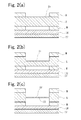
- the substrate S on which the mask M is formed is fixed on the adhesive surface of the heat-conductive sheet 26 disposed on the base 27 with a surface S1 facing upward (see Fig. 2(a) ).
- the base 27 is placed on the electrostatic chuck electrode 22 in the vacuum chamber 11.
- An etching gas is then introduced from means 4 for introducing an etching gas, and RF power is applied by the second high-frequency power source 43 to generate plasma in the plasma generation chamber 14, thereby etching the surface S1 of the substrate S to be processed (see Fig. 2(b) ).
- Etching of the substrate S on both sides further involves detaching the substrate S from the heat-conductive sheet 26 and reversing the substrate S, fixing the substrate S on the heat-conductive sheet 26 with a surface S2 facing upward, and etching the surface S2 under the substantially same conditions (see Fig. 2(c) ).
- use of the heat-conductive sheet 26 prevents the occurrence of a crack in the substrate S, providing the substrate S etched as desired.
- the temperature may be increased with a hot plate, an air-heating furnace, or near-infrared rays to, for example, approximately 170°C at which the heat-conductive sheet can be detached.
- the etching gas examples include gases that contain a fluorocarbon gas and at least one gas selected from rare gases, such as Ar, Xe, and Kr.
- the fluorocarbon gas examples include CF 4 , C 2 F 6 , C 4 F 8 , and C 3 F 8 . In particular, C 4 F 8 and C 3 F 8 are preferred.
- the rare gas is introduced by the gas-flow control means 32 such that the rare gas constitutes 80% to 95% of the total flow rate of the etching gas.
- the etching gas is introduced in a plasma atmosphere into a vacuum chamber 11 at an operating pressure of 1.0 Pa or less and a flow rate of 100 to 300 sccm, and etching is performed.
- a quartz substrate can be etched to a thickness of 10 ⁇ m.
- a substrate having a thickness in the range of 50 to 150 ⁇ m can be etched on both sides at a high aspect ratio, such as a width of 1 ⁇ m and a depth in the range of 20 to 70 ⁇ m.
- a quartz substrate was etched on both sides with an etching apparatus 1 illustrated in Fig. 1 .
- a thermal release sheet (Revalpha (trade name), thermal release temperature 170°C) having an adhesive layer on both sides manufactured by Nitto Denko Co. was prepared as a heat-conductive sheet 26.
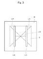
- Slits having shapes illustrated in Fig. 3 were formed in the heat-conductive sheet 26.
- the dotted line represents a substrate S to be attached.
- the heat-conductive sheet 26 had two linear slits L31 corresponding to the diagonal lines of the substrate, a single linear slit L32 parallel to the lateral direction of the substrate and passing through the center of the substrate, and two rectangular slits L33 parallel to the direction of the stripes of a mask.
- the heat-conductive sheet 26 having these slits was attached to a silicon base acting as the base 27.
- Ni masks were formed on a quartz substrate S to be processed (having a thickness of 100 ⁇ m) at intervals of 400 ⁇ m.
- the substrate S was fixed on the heat-conductive sheet 26.
- the silicon base was then placed on an electrostatic chuck electrode 22 of the etching apparatus 1.
- Plasma was generated with a second high-frequency power source 43.
- 100 sccm of etching gas including C 4 F 8 gas and Ar gas Ar gas constituted 80% of the total flow rate of the etching gas
- Etching conditions included a first high-frequency power source (substrate side) 550 W, a second high-frequency power source (antenna side) 1800 W, a substrate set temperature of 10°C, and a pressure of 0.67 Pa.
- the quartz substrate was etched by approximately 45 ⁇ m while the etching gas was introduced for 50 minutes.
- the silicon base was then removed from the etching apparatus 1.
- the substrate S was detached from the heat-conductive sheet on a hot plate at 120°C.
- the substrate S was then reversed and was fixed on the heat-conductive sheet with an unetched surface facing upward.
- the substrate S was etched again by approximately 45 ⁇ m under the substantially same conditions while the etching gas was introduced for 50 minutes.
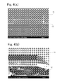
- Fig. 4(a) shows a cross-sectional SEM photograph of the resulting substrate
- 4(b) shows an SEM photograph of the substrate viewed from obliquely above.
- Figs. 4(a) and 4(b) show that surfaces S1 and S2 of the substrate S were etched and that the substrate S was etched on both sides without a crack, leaving only a very thin central portion (approximately 10 ⁇ m).
- Etching was performed under the same conditions as in Example 1, except that the substrate was placed on the silicon base directly rather than through the heat-conductive sheet. After etching of a surface, the silicon base was removed, and a crack was observed in the substrate. The direct installation of the substrate on the base probably resulted in low thermal conductivity and insufficient cooling. The substrate was therefore subjected to high temperature to form a crack.
- Etching was performed under the same conditions as in Example 1, except that the substrate S was fixed on a heat-conductive paste applied to the silicon base without providing the heat-conductive sheet. After etching of the backside, the silicon base was removed, and a crack was observed in the substrate S. Gas bubbles in the paste were probably thermally expanded and caused a crack in the substrate S. Removal of the heat-conductive paste required ultrasonic cleaning in alcohol. After the ultrasonic cleaning, additional fine cracks formed in the substrate.
- Etching was performed under the same conditions as in Example 1, except that the heat-conductive sheet had slits having the shapes illustrated in Fig. 5(a) (linear slits L51 on the diagonal lines of the substrate and a linear slit L51 parallel to a side of the substrate). After etching of a surface, the silicon base was removed, and it was observed that no crack formed in the substrate but a metal mask was detached.
- Etching was performed under the same conditions as in Example 1, except that the heat-conductive sheet had a slit having the shape illustrated in Fig. 5(b) (a polygonal slit L52 corresponding to the diagonal lines of the substrate). After etching of a surface, the silicon base was removed, and it was observed that a crack formed in the substrate and a metal mask was detached.
- Etching was performed under the same conditions as in Example 1, except that the heat-conductive sheet had slits having the shapes illustrated in Fig. 5(c) (two rectangular slits L53 parallel to the direction of the stripes of the mask). After etching of a surface, the silicon base was removed, and it was observed that a crack formed in the substrate and a metal mask was detached.
- Etching was performed under the same conditions as in Example 1, except that the heat-conductive sheet had a slit having the shape illustrated in Fig. 5(d) (a cross-shaped polygonal slit L54 passing through the center of the substrate). After etching of a surface, the silicon base was removed, and it was observed that a crack formed in the substrate and a metal mask was detached.
- a substrate can be stably etched on both sides.
- the present invention can be utilized in the semiconductor technical field.
Landscapes
- Engineering & Computer Science (AREA)
- Manufacturing & Machinery (AREA)
- Drying Of Semiconductors (AREA)
- Piezo-Electric Or Mechanical Vibrators, Or Delay Or Filter Circuits (AREA)
Abstract


Description
- The present invention relates to a dry etching method.
- In conventional dry etching apparatuses, electrostatic chucks and mechanical chucks have been used as mechanisms for fixing a substrate. One example of electrostatic chucks is a bipolar electrostatic chuck that includes an electrostatic chuck electrode. The electrostatic chuck electrode includes a circular first electrode and second electrodes. The second electrodes include a central electrode on the central side of the first electrode, corresponding to the central portion of a wafer, and a surrounding electrode outside the first electrode. A wafer is chucked on the top surface of the electrostatic chuck electrode by electrostatic forces generated between the first electrode and the second electrodes (see, for example, Patent Document 1). In this bipolar electrostatic chuck, helium gas is supplied to a narrow space between the wafer and the electrostatic chuck electrode to cool a substrate to be processed.
- To meet recent demands for miniaturization of electronic devices and communication devices, in quartz oscillators (crystal oscillators) serving as key devices, ultrasmall quartz oscillators having a quartz element size of approximately 1.2 mm have been manufactured by photolithography and practically used. However, there is a demand for still finer quartz oscillators on the order of micrometers. It is known that quartz oscillators of such an order are formed by micromachining a quartz substrate by a dry etching method because quartz oscillators of such an order cannot be processed mechanically (see, for example, Patent Document 2). In this case, a substrate is etched on both sides or etched very deeply on one side to form a quartz oscillator.
- Patent Document 1: Japanese Patent Application Publication No.
10-125769 - Patent Document 2: Japanese Patent Application Publication No.
2006-186847 Fig. 2 ) - However, when a substrate is continuously etched on both sides or etched very deeply on one side with an etching apparatus having an electrostatic chuck as described above, as the thickness of the substrate to be processed decreases, the substrate has a decreased strength and is susceptible to temperature changes. Thus, a crack may form in the substrate. Furthermore, cooling helium gas present between the substrate and an electrostatic chuck electrode may leak from the crack.
- It is an object of the present invention to solve the problems of the prior art and to provide a dry etching method for micromachining a substrate while the substrate is fixed so as not to form a crack even when the substrate is etched on both sides or etched very deeply on one side.
- A dry etching method according to the present invention comprises: introducing an etching gas including a fluorocarbon gas and a rare gas into a vacuum chamber; generating plasma in the vacuum chamber having a predetermined pressure; and etching a substrate adhered on an adhesive surface of a heat-conductive sheet disposed on a substrate table. Fixing a substrate on a heat-conductive sheet allows the entire substrate to be uniformly supported and promotes heat conduction to the substrate, which facilitates control of the temperature of the substrate. The substrate can therefore be etched as desired without causing a crack.
- A dry etching method according to the present invention comprises: introducing an etching gas including a fluorocarbon gas and a rare gas into a vacuum chamber; generating plasma in the vacuum chamber having a predetermined pressure; etching one side of a substrate to be processed adhered on an adhesive surface of a heat-conductive sheet disposed on a substrate table; detaching the substrate from the heat-conductive sheet and reversing the substrate; adhering the one side on the adhesive surface of the heat-conductive sheet; and etching the other side of the substrate under substantially same conditions as conditions for the one side. Fixing a substrate on a heat-conductive sheet allows the entire substrate to be uniformly supported and promotes heat conduction to the substrate, which facilitates control of the temperature of the substrate. Both sides of the substrate can therefore be etched.
- In this case, the substrate is preferably detached from the heat-conductive sheet by heating or UV irradiation. Damage for the substrate can be reduced by detaching the substrate through such a process. Preferably, the substrate is a quartz substrate. Preferably, the heat-conductive sheet has a slit. The slit facilitates the detachment of the substrate from the heat-conductive sheet and decreases air bubbles under the heat-conductive sheet.
- In etching, the flow rate of the rare gas preferably ranges from 80% to 95% of the total flow rate of the etching gas, and the rare gas is preferably at least one of Ar, Kr, and Xe. The flow rate of the rare gas below 80% of the total flow rate results in an excessively large number of active species, and etching cannot be performed as desired. The flow rate of the rare gas above 95% results in an excessively small number of active species, and etching cannot be performed sufficiently.
- Preferably, the dry etching method is performed in a low-pressure process at 1 Pa or less. At a pressure above 1 Pa, radical reactions are difficult to prevent, making micromachining difficult.
A dry etching method according to the present invention comprises: fixing a heat-conductive sheet on a base; adhering a quartz substrate on an adhesive surface of the heat-conductive sheet; placing the base on a substrate table in a vacuum chamber; introducing an etching gas including a fluorocarbon gas and a rare gas into the vacuum chamber; forming a magnetic neutral line while maintaining the internal pressure of the vacuum chamber at 1 Pa or less; applying an electric field to generate plasma in the vacuum chamber; etching one side of the quartz substrate; detaching the quartz substrate from the heat-conductive sheet and reversing the substrate; adhering the one side of the quartz substrate on the adhesive surface of the heat-conductive sheet; and etching the other side of the quartz substrate under substantially same conditions as conditions for the one side. In etching of a quartz substrate fixed on a heat-conductive sheet using a dry etching apparatus that forms a magnetic neutral line and generates plasma, both sides of the substrate can be etched as desired with high-efficiency plasma while the entire substrate is uniformly supported.
In this case, preferably, the flow rate of the rare gas ranges from 80% to 95% of the total flow rate of the etching gas, the rare gas is at least one of Ar, Kr, and Xe, the heat-conductive sheet has a slit, and the substrate is detached from the heat-conductive sheet by heating or UV irradiation. - A dry etching method according to the present invention allows a substrate to be etched simply as desired without causing a crack in the substrate.
-
Fig. 1 illustrates anetching apparatus 1 used for performing a method for dry-etching an interlayer insulating film according to the present invention. Theetching apparatus 1 includes avacuum chamber 11 and can perform etching with low-temperature and high-density plasma. Thevacuum chamber 11 is provided with evacuation means 12, such as a turbo-molecular pump. - The
vacuum chamber 11 includes a lowersubstrate processing chamber 13 and an upperplasma generation chamber 14. A substrate table 2 is disposed at the center of the bottom of thesubstrate processing chamber 13. The substrate table 2 includes asubstrate electrode 21, anelectrostatic chuck electrode 22 disposed on thesubstrate electrode 21, and asupport 23 for supporting thesubstrate electrode 21 and theelectrostatic chuck electrode 22. Thesubstrate electrode 21 is connected to a first high-frequency power source 25 via a blockingcapacitor 24, acts as a floating electrode in terms of electric potential, and has negative bias potential. Theelectrostatic chuck electrode 22 may be a known electrostatic chuck electrode. - In the present invention, a
base 27 on which a heat-conductive sheet 26 is placed is fixed with anelectrostatic chuck electrode 22, and a substrate S to be processed is adhered on an adhesive surface of the heat-conductive sheet. Fixing the substrate S on the adhesive surface obviates the necessity of fixing the substrate S with an electrostatic chuck electrode, allowing the entire substrate S to be held stably and preventing the occurrence of a crack in the substrate. With such a structure, helium gas (not shown) in theelectrostatic chuck electrode 22 has a cooling effect on the substrate S through the heat-conductive sheet 26, allowing the temperature of the substrate S to be controlled and preventing the occurrence of a crack in the substrate S. - Examples of the material of an adhesive layer in the heat-
conductive sheet 26 include heat-conductive resins, for example, rubber, such as acrylic or isoprene isobutylene, or resins, such as silicone. The material of an adhesive layer may be any material provided that the adhesive layer can be detached by heating or UV irradiation. The heat-conductive sheet 26 has at least one heat-conductive adhesive surface. - A heat-
conductive sheet 26 having a slit may be attached on thebase 27. The slit facilitates the detachment of the heat-conductive sheet, and, in some cases, the slit prevents present the occurrence of a crack in the substrate due to the gas, such as air or an etching gas incorporated by evacuation, present between the heat-conductive sheet and the base (i.e., generation of gas bubbles). The shape of the slit may be not only linear, but also polygonal, circular, or a combination thereof. For example, in etching with a striped mask, preferably, a first slit is formed on a diagonal line of a substrate, and a second slit is formed in the direction of the stripes of the striped mask. After a heat-conductive sheet is fixed on the base, the heat-conductive sheet is preferably pressed with a rubber roller, a paddle, or a press machine to prevent such gas from being incorporated between the heat-conductive sheet and the base. - The substrate table 2 faces a
top plate 15, which is disposed at the top of theplasma generation chamber 14 and is fixed to the sidewall of theplasma generation chamber 14. Thetop plate 15 is connected to a gas-inlet line 31 of gas-inlet means 3, which introduce an etching gas into thevacuum chamber 11. The gas-inlet line 31 has two branches, which lead to arare gas source 33 and afluorocarbon gas source 34 via gas-flow control means 32. - The
top plate 15 may include a shower plate connected to the gas-inlet means 3. - The
plasma generation chamber 14 has a cylindrical dielectric sidewall. Amagnetic field coil 41 is disposed outside the sidewall as means for generating a magnetic field. Themagnetic field coil 41 forms a magnetic neutral loop (not shown) in theplasma generation chamber 14. - A high-frequency antenna coil 42 for generating plasma is disposed between the
magnetic field coil 41 and the outside of the sidewall of theplasma generation chamber 14. The high-frequency antenna coil 42 has a parallel antenna structure and constructed such that a voltage can be applied to the high-frequency antenna coil 42 by a second high-frequency power source 43. After a magnetic neutral line is formed by themagnetic field coil 41, an alternating electric field is applied along the magnetic neutral line to generate discharge plasma along the magnetic neutral line. - A mechanism for adjusting the voltage applied to the antenna coil to a predetermined voltage may be disposed.
- An etching apparatus thus constituted has a simple structure and can form high-efficiency plasma without mutual interference of applied high-frequency electric fields.
- An etching apparatus for performing a dry etching method according to the present invention may include a Faraday shield-like (or electrostatic field shield-like) floating electrode (not shown) inside the high-frequency antenna coil 42. The Faraday shield is a known Faraday shield and is, for example, a metal plate that has a plurality of parallel slits and an antenna coil intersecting the slits at right angles at the longitudinal midpoints of the slits. A metallic frame for equalizing the electric potential of a strip of metal plate is disposed at each longitudinal end of the slits. The metal plate can shield against an electrostatic field of the antenna coil 42 but cannot shield against an induction magnetic field. The induction magnetic field enters plasma and forms an induction electric field. The width of the slit can be appropriately determined for each purpose and ranges from 0.5 to 10 mm, preferably 1 to 2 mm. An excessively wide slit unfavorably causes the penetration of an electrostatic field. The slits may have a thickness of approximately 2 mm.
- A method for etching a substrate S to be processed on both sides with the above-described
etching apparatus 1 will be described below with reference toFigs. 1 and2 . - An object to be etched with the
etching apparatus 1 is preferably a quartz substrate. A quartz substrate itself can be processed to manufacture, for example, a crystal oscillator on the order of micrometers, which has not been manufactured by conventional machining. A generally-used substrate on which a SiO2 film, a film of a compound containing SiO2 or a film formed of a material for optical elements is formed may be processed. - Examples of the compound containing SiO2 include TEOS-SiO2, phosphosilicate glass, borophosphosilicate glass, rare-earth-doped glass, and low-expansion crystallized-glass. Examples of the material for optical elements include lithium niobate, lithium tantalate, titanium oxide, tantalum oxide, and bismuth oxide.
- The substrate may include a SiOCH material film formed by spin coating, such as HSQ or MSQ, a Low-k material film, which is formed of a SiOC material and is formed by CVD and has a relative dielectric constant in the range of 2.0 to 3.2, or a porous material film.
- Examples of the SiOCH material include LKD5109r5 (trade name) manufactured by JSR Co., HSG-7000 (trade name) manufactured by Hitachi Chemical Co., Ltd., HOSP (trade name) manufactured by Honeywell Electric Materials, Nanoglass (trade name) manufactured by Honeywell Electric Materials, OCD T-12 (trade name) manufactured by Tokyo Ohka Kogyo Co., Ltd., OCD T-32 (trade name) manufactured by Tokyo Ohka Kogyo Co., Ltd., IPS2.4 (trade name) manufactured by Catalysts & Chemicals Industries Co., Ltd., IPS2.2 (trade name) manufactured by Catalysts & Chemicals Industries Co., Ltd., ALCAP-S5100 (trade name) manufactured by Asahi Kasei Co., and ISM (trade name) manufactured by ULVAC, Inc.
- Examples of the SiOC material include Aurola2.7 (trade name) manufactured by ASM Japan K.K., Aurola2.4 (trade name) manufactured by ASM Japan K.K., Orion2.2 (trade name) manufactured by Fastgate Co. and Trikon Technologies Inc., Coral (trade name) manufactured by Novellus Systems Inc., Black Diamond (trade name) manufactured by Applied Materials, Inc. (AMAT), and NCS (trade name) manufactured by Fujitsu Ltd. Examples of the SiOC material also include SiLK (trade name) manufactured by The Dow Chemical Company, Porous-SiLK (trade name) manufactured by The Dow Chemical Company, FLARE (trade name) manufactured by Honeywell Electric Materials, Porous FLARE (trade name) manufactured by Honeywell Electric Materials, and GX-3P (trade name) manufactured by Honeywell Electric Materials.
- As illustrated in
Figs. 2(a) to 2(c) , a mask M is formed on the substrate S to be etched. Examples of the material of the mask include organic materials, such as KrF resist materials and ArF resist materials, and known metallic materials, such as Ni. - The substrate S on which the mask M is formed is fixed on the adhesive surface of the heat-
conductive sheet 26 disposed on the base 27 with a surface S1 facing upward (seeFig. 2(a) ). Thebase 27 is placed on theelectrostatic chuck electrode 22 in thevacuum chamber 11. An etching gas is then introduced from means 4 for introducing an etching gas, and RF power is applied by the second high-frequency power source 43 to generate plasma in theplasma generation chamber 14, thereby etching the surface S1 of the substrate S to be processed (seeFig. 2(b) ). Etching of the substrate S on both sides further involves detaching the substrate S from the heat-conductive sheet 26 and reversing the substrate S, fixing the substrate S on the heat-conductive sheet 26 with a surface S2 facing upward, and etching the surface S2 under the substantially same conditions (seeFig. 2(c) ). Thus, even when the substrate S has a very small thickness after etching of both sides, use of the heat-conductive sheet 26 prevents the occurrence of a crack in the substrate S, providing the substrate S etched as desired. - To detach a heat-conductive sheet by heating, the temperature may be increased with a hot plate, an air-heating furnace, or near-infrared rays to, for example, approximately 170°C at which the heat-conductive sheet can be detached.
- Examples of the etching gas include gases that contain a fluorocarbon gas and at least one gas selected from rare gases, such as Ar, Xe, and Kr. Examples of the fluorocarbon gas include CF4, C2F6, C4F8, and C3F8. In particular, C4F8 and C3F8 are preferred. In this case, the rare gas is introduced by the gas-flow control means 32 such that the rare gas constitutes 80% to 95% of the total flow rate of the etching gas. The etching gas is introduced in a plasma atmosphere into a
vacuum chamber 11 at an operating pressure of 1.0 Pa or less and a flow rate of 100 to 300 sccm, and etching is performed. - According to a dry etching method using such a
dry etching apparatus 1, a quartz substrate can be etched to a thickness of 10 µm. For example, a substrate having a thickness in the range of 50 to 150 µm can be etched on both sides at a high aspect ratio, such as a width of 1µm and a depth in the range of 20 to 70 µm. - In the present example, a quartz substrate was etched on both sides with an
etching apparatus 1 illustrated inFig. 1 . - A thermal release sheet (Revalpha (trade name), thermal release temperature 170°C) having an adhesive layer on both sides manufactured by Nitto Denko Co. was prepared as a heat-
conductive sheet 26. Slits having shapes illustrated inFig. 3 were formed in the heat-conductive sheet 26. InFig. 3 , the dotted line represents a substrate S to be attached. The heat-conductive sheet 26 had two linear slits L31 corresponding to the diagonal lines of the substrate, a single linear slit L32 parallel to the lateral direction of the substrate and passing through the center of the substrate, and two rectangular slits L33 parallel to the direction of the stripes of a mask. The heat-conductive sheet 26 having these slits was attached to a silicon base acting as thebase 27. Ni masks were formed on a quartz substrate S to be processed (having a thickness of 100 µm) at intervals of 400 µm. The substrate S was fixed on the heat-conductive sheet 26. The silicon base was then placed on anelectrostatic chuck electrode 22 of theetching apparatus 1. Plasma was generated with a second high-frequency power source 43. 100 sccm of etching gas including C4F8 gas and Ar gas (Ar gas constituted 80% of the total flow rate of the etching gas) was introduced, and the substrate S to be processed was etched. Etching conditions included a first high-frequency power source (substrate side) 550 W, a second high-frequency power source (antenna side) 1800 W, a substrate set temperature of 10°C, and a pressure of 0.67 Pa. - The quartz substrate was etched by approximately 45 µm while the etching gas was introduced for 50 minutes. The silicon base was then removed from the
etching apparatus 1. The substrate S was detached from the heat-conductive sheet on a hot plate at 120°C. The substrate S was then reversed and was fixed on the heat-conductive sheet with an unetched surface facing upward. The substrate S was etched again by approximately 45 µm under the substantially same conditions while the etching gas was introduced for 50 minutes.Fig. 4(a) shows a cross-sectional SEM photograph of the resulting substrate, and 4(b) shows an SEM photograph of the substrate viewed from obliquely above. -
Figs. 4(a) and 4(b) show that surfaces S1 and S2 of the substrate S were etched and that the substrate S was etched on both sides without a crack, leaving only a very thin central portion (approximately 10 µm). - Etching was performed under the same conditions as in Example 1, except that the substrate was placed on the silicon base directly rather than through the heat-conductive sheet. After etching of a surface, the silicon base was removed, and a crack was observed in the substrate. The direct installation of the substrate on the base probably resulted in low thermal conductivity and insufficient cooling. The substrate was therefore subjected to high temperature to form a crack.
- Etching was performed under the same conditions as in Example 1, except that the substrate S was fixed on a heat-conductive paste applied to the silicon base without providing the heat-conductive sheet. After etching of the backside, the silicon base was removed, and a crack was observed in the substrate S. Gas bubbles in the paste were probably thermally expanded and caused a crack in the substrate S. Removal of the heat-conductive paste required ultrasonic cleaning in alcohol. After the ultrasonic cleaning, additional fine cracks formed in the substrate.
- Etching was performed under the same conditions as in Example 1, except that the heat-conductive sheet had slits having the shapes illustrated in
Fig. 5(a) (linear slits L51 on the diagonal lines of the substrate and a linear slit L51 parallel to a side of the substrate). After etching of a surface, the silicon base was removed, and it was observed that no crack formed in the substrate but a metal mask was detached. - Etching was performed under the same conditions as in Example 1, except that the heat-conductive sheet had a slit having the shape illustrated in
Fig. 5(b) (a polygonal slit L52 corresponding to the diagonal lines of the substrate). After etching of a surface, the silicon base was removed, and it was observed that a crack formed in the substrate and a metal mask was detached. - Etching was performed under the same conditions as in Example 1, except that the heat-conductive sheet had slits having the shapes illustrated in
Fig. 5(c) (two rectangular slits L53 parallel to the direction of the stripes of the mask). After etching of a surface, the silicon base was removed, and it was observed that a crack formed in the substrate and a metal mask was detached. - Etching was performed under the same conditions as in Example 1, except that the heat-conductive sheet had a slit having the shape illustrated in
Fig. 5(d) (a cross-shaped polygonal slit L54 passing through the center of the substrate). After etching of a surface, the silicon base was removed, and it was observed that a crack formed in the substrate and a metal mask was detached. - According to the above-described results demonstrate that only when the heat-conductive sheet having the slits in the shapes described in Example 1 is used, the quartz substrate can be etched on both sides with the
etching apparatus 1. - According to a dry etching method of the present invention, a substrate can be stably etched on both sides. Thus, the present invention can be utilized in the semiconductor technical field.
-
-
Fig. 1 is a schematic view of a dry etching apparatus for use in a dry etching method according to the present invention. -
Figs. 2(a) to 2(c) are schematic views illustrating a double-sided dry etching method according to the present invention. -
Fig. 3 is a schematic view of the shape of slits in a heat-conductive sheet used in Example 1. -
Figs. 4(a) and 4(b) are SEM photographs indicating the results of Example 1: 4(a) is a cross-sectional SEM photograph of a substrate, and 4(b) is an SEM photograph of the substrate viewed from obliquely above. -
Figs. 5(a) to 5(d) are schematic views illustrating the shapes of slits in heat-conductive sheets used in Comparative Examples 3 to 6: 5(a) for Comparative Example 3, 5(b) for Comparative Example 4, 5(c) for Comparative Example 5, and 5(d) for Comparative Example 6. -
- 1
- etching apparatus
- 2
- substrate table
- 3
- etching gas-inlet means
- 11
- vacuum chamber
- 12
- evacuation means
- 13
- substrate processing chamber
- 14
- plasma generation chamber
- 15
- top plate
- 21
- substrate electrode
- 22
- electrostatic chuck electrode
- 23
- support
- 24
- blocking capacitor
- 25
- high-frequency power source
- 26
- heat-conductive sheet
- 27
- base
- 31
- gas-inlet line
- 32
- gas-flow control means
- 33
- rare gas source
- 34
- fluorocarbon gas source
- 41
- magnetic field coil
- 42
- antenna coil
- 42
- high-frequency antenna coil
- 43
- high-frequency power source
- S
- substrate to be processed
- L31, L32, L33
- slit
Claims (10)
- A dry etching method comprising:introducing an etching gas including a fluorocarbon gas and a rare gas into a vacuum chamber;generating plasma in the vacuum chamber having a predetermined pressure; andetching a substrate adhered on an adhesive surface of a heat-conductive sheet disposed on a substrate table.
- A dry etching method comprising:introducing an etching gas including a fluorocarbon gas and a rare gas into a vacuum chamber;generating plasma in the vacuum chamber having a predetermined pressure;etching one side of a substrate adhered on an adhesive surface of a heat-conductive sheet disposed on a substrate table;detaching the substrate from the heat-conductive sheet and reversing the substrate;adhering the one side on the adhesive surface of the heat-conductive sheet; andetching the other side of the substrate under substantially same conditions as conditions for the one side.
- The dry etching method according to claim 1 or 2, wherein the substrate is detached from the heat-conductive sheet by heating or UV irradiation.
- The dry etching method according to any one of claims 1 to 3, wherein the substrate is a quartz substrate.
- The dry etching method according to any one of claims 1 to 4, wherein the heat-conductive sheet has a slit.
- The dry etching method according to any one of claims 1 to 5, wherein the flow rate of the rare gas ranges from 80% to 95% of the total flow rate of the etching gas.
- The dry etching method according to any one of claims 1 to 6, wherein the rare gas is at least one of Ar, Kr, and Xe.
- The dry etching method according to any one of claims 1 to 7, wherein the dry etching method is performed in a low-pressure process at 1 Pa or less.
- A dry etching method comprising:fixing a heat-conductive sheet on a base;adhering a quartz substrate on an adhesive surface of the heat-conductive sheet;placing the base on a substrate table in a vacuum chamber;introducing an etching gas including a fluorocarbon gas and a rare gas into the vacuum chamber;forming a magnetic neutral line while maintaining the internal pressure of the vacuum chamber at 1 Pa or less;applying an electric field to generate plasma in the vacuum chamber; etching one side of the quartz substrate;detaching the quartz substrate from the heat-conductive sheet and reversing the substrate;adhering the one side of the quartz substrate on the adhesive surface of the heat-conductive sheet; andetching the other side of the quartz substrate under substantially same conditions as conditions for the one side.
- The dry etching method according to claim 9, wherein the flow rate of the rare gas ranges from 80% to 95% of the total flow rate of the etching gas, the rare gas is at least one of Ar, Kr, and Xe, the heat-conductive sheet has a slit, and the substrate is detached from the heat-conductive sheet by heating or UV irradiation.
Applications Claiming Priority (2)
| Application Number | Priority Date | Filing Date | Title |
|---|---|---|---|
| JP2007127789 | 2007-05-14 | ||
| PCT/JP2008/058534 WO2008143004A1 (en) | 2007-05-14 | 2008-05-08 | Dry etching method |
Publications (3)
| Publication Number | Publication Date |
|---|---|
| EP2148360A1 true EP2148360A1 (en) | 2010-01-27 |
| EP2148360A4 EP2148360A4 (en) | 2010-07-21 |
| EP2148360B1 EP2148360B1 (en) | 2014-01-22 |
Family
ID=40031716
Family Applications (1)
| Application Number | Title | Priority Date | Filing Date |
|---|---|---|---|
| EP08752425.2A Active EP2148360B1 (en) | 2007-05-14 | 2008-05-08 | Dry etching method |
Country Status (8)
| Country | Link |
|---|---|
| US (1) | US20100133233A1 (en) |
| EP (1) | EP2148360B1 (en) |
| JP (1) | JP5090443B2 (en) |
| KR (1) | KR101242464B1 (en) |
| CN (1) | CN101681826B (en) |
| AU (1) | AU2008252203A1 (en) |
| TW (1) | TWI449101B (en) |
| WO (1) | WO2008143004A1 (en) |
Families Citing this family (5)
| Publication number | Priority date | Publication date | Assignee | Title |
|---|---|---|---|---|
| JP5185847B2 (en) * | 2009-01-30 | 2013-04-17 | パナソニック株式会社 | Substrate dry etching method |
| JP5352777B2 (en) * | 2009-01-30 | 2013-11-27 | パナソニック株式会社 | Quartz device manufacturing method |
| JP5468325B2 (en) * | 2009-07-27 | 2014-04-09 | 株式会社アルバック | Device manufacturing method |
| CN110880444B (en) * | 2019-11-28 | 2022-04-12 | 河北工程大学 | A device for continuous double-sided etching of optical devices based on plasma etching |
| WO2024135385A1 (en) * | 2022-12-21 | 2024-06-27 | 東京エレクトロン株式会社 | Plasma processing device and control method |
Family Cites Families (18)
| Publication number | Priority date | Publication date | Assignee | Title |
|---|---|---|---|---|
| JPH10125769A (en) | 1996-10-21 | 1998-05-15 | Matsushita Electron Corp | Electrostatic chuck electrode structure |
| KR100278137B1 (en) * | 1997-09-04 | 2001-01-15 | 가나이 쓰도무 | Method of mounting semiconductor device and system thereof, method of manufacturing semiconductor device isolator and IC card |
| JPH11150133A (en) * | 1997-09-04 | 1999-06-02 | Hitachi Ltd | Semiconductor element mounting method and system, semiconductor element separation apparatus, and IC card manufacturing method |
| JP2001156584A (en) * | 1999-11-30 | 2001-06-08 | Sony Corp | Piezoelectric element and manufacturing method thereof |
| JP2002059363A (en) * | 2000-08-23 | 2002-02-26 | Chemitoronics Co Ltd | Wafer support |
| US6642127B2 (en) * | 2001-10-19 | 2003-11-04 | Applied Materials, Inc. | Method for dicing a semiconductor wafer |
| JP2003142979A (en) * | 2001-10-31 | 2003-05-16 | River Eletec Kk | Quartz crystal resonator and manufacturing method thereof |
| US20050178741A1 (en) * | 2003-05-03 | 2005-08-18 | Yeoh Joon C. | Method of etching porous dielectric |
| US20050036267A1 (en) * | 2003-05-20 | 2005-02-17 | Savas Stephen Edward | Clamp for holding and efficiently removing heat from workpieces |
| JP4500029B2 (en) * | 2003-09-22 | 2010-07-14 | 株式会社アルバック | Dry etching method for low dielectric constant interlayer insulating film |
| TWI231534B (en) * | 2003-12-11 | 2005-04-21 | Advanced Semiconductor Eng | Method for dicing a wafer |
| JP2005286992A (en) * | 2004-03-02 | 2005-10-13 | Seiko Epson Corp | Piezoelectric vibrating piece, piezoelectric vibrator and piezoelectric oscillator |
| TWI236058B (en) * | 2004-08-06 | 2005-07-11 | Touch Micro System Tech | Method of performing double side processes upon a wafer |
| JP4729924B2 (en) | 2004-12-28 | 2011-07-20 | エプソントヨコム株式会社 | Method for producing AT-cut crystal piece assembly |
| JP2007053189A (en) * | 2005-08-17 | 2007-03-01 | Konica Minolta Holdings Inc | Silicon substrate including mask pattern used for manufacture of silicon structure body and manufacturing method of silicon structure body |
| JP2007096756A (en) * | 2005-09-29 | 2007-04-12 | Seiko Epson Corp | Substrate manufacturing method, crystal vibrating piece, and gyro vibrating piece |
| TWI276844B (en) * | 2006-03-28 | 2007-03-21 | United Microelectronics Corp | Etching method |
| JP4197001B2 (en) * | 2006-04-04 | 2008-12-17 | エプソントヨコム株式会社 | Method for manufacturing piezoelectric vibrating piece |
-
2008
- 2008-05-08 JP JP2009515143A patent/JP5090443B2/en not_active Expired - Fee Related
- 2008-05-08 CN CN2008800159148A patent/CN101681826B/en active Active
- 2008-05-08 EP EP08752425.2A patent/EP2148360B1/en active Active
- 2008-05-08 KR KR1020097023612A patent/KR101242464B1/en active Active
- 2008-05-08 WO PCT/JP2008/058534 patent/WO2008143004A1/en not_active Ceased
- 2008-05-08 US US12/597,645 patent/US20100133233A1/en not_active Abandoned
- 2008-05-08 AU AU2008252203A patent/AU2008252203A1/en not_active Abandoned
- 2008-05-13 TW TW097117582A patent/TWI449101B/en active
Also Published As
| Publication number | Publication date |
|---|---|
| TWI449101B (en) | 2014-08-11 |
| CN101681826A (en) | 2010-03-24 |
| CN101681826B (en) | 2011-08-10 |
| US20100133233A1 (en) | 2010-06-03 |
| EP2148360A4 (en) | 2010-07-21 |
| TW200903633A (en) | 2009-01-16 |
| KR101242464B1 (en) | 2013-03-12 |
| KR20100016479A (en) | 2010-02-12 |
| AU2008252203A1 (en) | 2008-11-27 |
| WO2008143004A1 (en) | 2008-11-27 |
| EP2148360B1 (en) | 2014-01-22 |
| JPWO2008143004A1 (en) | 2010-08-05 |
| JP5090443B2 (en) | 2012-12-05 |
Similar Documents
| Publication | Publication Date | Title |
|---|---|---|
| CN102097353B (en) | Method of protecting a bond layer in a substrate support adapted for use in a plasma processing system | |
| KR101811910B1 (en) | Method of etching features in silicon nitride films | |
| US9299580B2 (en) | High aspect ratio plasma etch for 3D NAND semiconductor applications | |
| TWI605503B (en) | Method of forming features in a material layer using a combination of a primary etch and a cycle etch process | |
| US8389416B2 (en) | Process for etching silicon with selectivity to silicon-germanium | |
| TWI338725B (en) | Methods for etching dielectric materials | |
| KR20210037318A (en) | Substrate processing apparatus and method, and semiconductor device manufacturing method using the processing method | |
| EP2148360B1 (en) | Dry etching method | |
| WO2012047459A2 (en) | Selective etch process for silicon nitride | |
| EP2148361A1 (en) | Dry etching apparatus and dry etching method | |
| US20220319841A1 (en) | Deposition of low-stress carbon-containing layers | |
| EP3627538A1 (en) | Method for etching porous film | |
| JP2004319972A (en) | Etching method and etching apparatus | |
| WO2004097909A2 (en) | Method and apparatus for deep trench silicon etch | |
| KR20110006932A (en) | Board retainer | |
| US20210202207A1 (en) | Plasma processing method, and element chip manufacturing method | |
| US7189653B2 (en) | Etching method and etching apparatus | |
| CN102263021B (en) | Method for preparing low voltage gate oxide | |
| US20200303203A1 (en) | Method of etching film and plasma processing apparatus | |
| US11791155B2 (en) | Diffusion barriers for germanium | |
| JP2005026348A (en) | Plasma processing method | |
| JP4990551B2 (en) | Dry etching method | |
| US20070077772A1 (en) | Apparatus and method for manufacturing semiconductor device using plasma | |
| KR19990065751A (en) | Chamber equipment for manufacturing a semiconductor device comprising an anode having a cooling line for cooling the back of the semiconductor substrate |
Legal Events
| Date | Code | Title | Description |
|---|---|---|---|
| PUAI | Public reference made under article 153(3) epc to a published international application that has entered the european phase |
Free format text: ORIGINAL CODE: 0009012 |
|
| 17P | Request for examination filed |
Effective date: 20091109 |
|
| AK | Designated contracting states |
Kind code of ref document: A1 Designated state(s): AT BE BG CH CY CZ DE DK EE ES FI FR GB GR HR HU IE IS IT LI LT LU LV MC MT NL NO PL PT RO SE SI SK TR |
|
| AX | Request for extension of the european patent |
Extension state: AL BA MK RS |
|
| RIN1 | Information on inventor provided before grant (corrected) |
Inventor name: MORIKAWA, YASUHIRO Inventor name: HAYASHI, TOSHIO Inventor name: SATOU, TADAYUKI Inventor name: SUU, KOUKOU |
|
| A4 | Supplementary search report drawn up and despatched |
Effective date: 20100617 |
|
| DAX | Request for extension of the european patent (deleted) | ||
| GRAP | Despatch of communication of intention to grant a patent |
Free format text: ORIGINAL CODE: EPIDOSNIGR1 |
|
| INTG | Intention to grant announced |
Effective date: 20130812 |
|
| GRAS | Grant fee paid |
Free format text: ORIGINAL CODE: EPIDOSNIGR3 |
|
| GRAA | (expected) grant |
Free format text: ORIGINAL CODE: 0009210 |
|
| AK | Designated contracting states |
Kind code of ref document: B1 Designated state(s): AT BE BG CH CY CZ DE DK EE ES FI FR GB GR HR HU IE IS IT LI LT LU LV MC MT NL NO PL PT RO SE SI SK TR |
|
| REG | Reference to a national code |
Ref country code: GB Ref legal event code: FG4D |
|
| REG | Reference to a national code |
Ref country code: CH Ref legal event code: EP |
|
| REG | Reference to a national code |
Ref country code: AT Ref legal event code: REF Ref document number: 651126 Country of ref document: AT Kind code of ref document: T Effective date: 20140215 |
|
| REG | Reference to a national code |
Ref country code: IE Ref legal event code: FG4D |
|
| REG | Reference to a national code |
Ref country code: DE Ref legal event code: R096 Ref document number: 602008030085 Country of ref document: DE Effective date: 20140306 |
|
| REG | Reference to a national code |
Ref country code: NL Ref legal event code: VDEP Effective date: 20140122 |
|
| REG | Reference to a national code |
Ref country code: AT Ref legal event code: MK05 Ref document number: 651126 Country of ref document: AT Kind code of ref document: T Effective date: 20140122 |
|
| REG | Reference to a national code |
Ref country code: LT Ref legal event code: MG4D |
|
| PG25 | Lapsed in a contracting state [announced via postgrant information from national office to epo] |
Ref country code: LT Free format text: LAPSE BECAUSE OF FAILURE TO SUBMIT A TRANSLATION OF THE DESCRIPTION OR TO PAY THE FEE WITHIN THE PRESCRIBED TIME-LIMIT Effective date: 20140122 Ref country code: NO Free format text: LAPSE BECAUSE OF FAILURE TO SUBMIT A TRANSLATION OF THE DESCRIPTION OR TO PAY THE FEE WITHIN THE PRESCRIBED TIME-LIMIT Effective date: 20140422 Ref country code: IS Free format text: LAPSE BECAUSE OF FAILURE TO SUBMIT A TRANSLATION OF THE DESCRIPTION OR TO PAY THE FEE WITHIN THE PRESCRIBED TIME-LIMIT Effective date: 20140522 |
|
| PG25 | Lapsed in a contracting state [announced via postgrant information from national office to epo] |
Ref country code: FI Free format text: LAPSE BECAUSE OF FAILURE TO SUBMIT A TRANSLATION OF THE DESCRIPTION OR TO PAY THE FEE WITHIN THE PRESCRIBED TIME-LIMIT Effective date: 20140122 Ref country code: NL Free format text: LAPSE BECAUSE OF FAILURE TO SUBMIT A TRANSLATION OF THE DESCRIPTION OR TO PAY THE FEE WITHIN THE PRESCRIBED TIME-LIMIT Effective date: 20140122 Ref country code: CY Free format text: LAPSE BECAUSE OF FAILURE TO SUBMIT A TRANSLATION OF THE DESCRIPTION OR TO PAY THE FEE WITHIN THE PRESCRIBED TIME-LIMIT Effective date: 20140122 Ref country code: SE Free format text: LAPSE BECAUSE OF FAILURE TO SUBMIT A TRANSLATION OF THE DESCRIPTION OR TO PAY THE FEE WITHIN THE PRESCRIBED TIME-LIMIT Effective date: 20140122 Ref country code: AT Free format text: LAPSE BECAUSE OF FAILURE TO SUBMIT A TRANSLATION OF THE DESCRIPTION OR TO PAY THE FEE WITHIN THE PRESCRIBED TIME-LIMIT Effective date: 20140122 Ref country code: ES Free format text: LAPSE BECAUSE OF FAILURE TO SUBMIT A TRANSLATION OF THE DESCRIPTION OR TO PAY THE FEE WITHIN THE PRESCRIBED TIME-LIMIT Effective date: 20140122 Ref country code: PT Free format text: LAPSE BECAUSE OF FAILURE TO SUBMIT A TRANSLATION OF THE DESCRIPTION OR TO PAY THE FEE WITHIN THE PRESCRIBED TIME-LIMIT Effective date: 20140522 |
|
| PG25 | Lapsed in a contracting state [announced via postgrant information from national office to epo] |
Ref country code: HR Free format text: LAPSE BECAUSE OF FAILURE TO SUBMIT A TRANSLATION OF THE DESCRIPTION OR TO PAY THE FEE WITHIN THE PRESCRIBED TIME-LIMIT Effective date: 20140122 Ref country code: LV Free format text: LAPSE BECAUSE OF FAILURE TO SUBMIT A TRANSLATION OF THE DESCRIPTION OR TO PAY THE FEE WITHIN THE PRESCRIBED TIME-LIMIT Effective date: 20140122 Ref country code: BE Free format text: LAPSE BECAUSE OF FAILURE TO SUBMIT A TRANSLATION OF THE DESCRIPTION OR TO PAY THE FEE WITHIN THE PRESCRIBED TIME-LIMIT Effective date: 20140122 |
|
| REG | Reference to a national code |
Ref country code: DE Ref legal event code: R097 Ref document number: 602008030085 Country of ref document: DE |
|
| PG25 | Lapsed in a contracting state [announced via postgrant information from national office to epo] |
Ref country code: RO Free format text: LAPSE BECAUSE OF FAILURE TO SUBMIT A TRANSLATION OF THE DESCRIPTION OR TO PAY THE FEE WITHIN THE PRESCRIBED TIME-LIMIT Effective date: 20140122 Ref country code: EE Free format text: LAPSE BECAUSE OF FAILURE TO SUBMIT A TRANSLATION OF THE DESCRIPTION OR TO PAY THE FEE WITHIN THE PRESCRIBED TIME-LIMIT Effective date: 20140122 Ref country code: DK Free format text: LAPSE BECAUSE OF FAILURE TO SUBMIT A TRANSLATION OF THE DESCRIPTION OR TO PAY THE FEE WITHIN THE PRESCRIBED TIME-LIMIT Effective date: 20140122 Ref country code: CZ Free format text: LAPSE BECAUSE OF FAILURE TO SUBMIT A TRANSLATION OF THE DESCRIPTION OR TO PAY THE FEE WITHIN THE PRESCRIBED TIME-LIMIT Effective date: 20140122 |
|
| PG25 | Lapsed in a contracting state [announced via postgrant information from national office to epo] |
Ref country code: PL Free format text: LAPSE BECAUSE OF FAILURE TO SUBMIT A TRANSLATION OF THE DESCRIPTION OR TO PAY THE FEE WITHIN THE PRESCRIBED TIME-LIMIT Effective date: 20140122 Ref country code: SK Free format text: LAPSE BECAUSE OF FAILURE TO SUBMIT A TRANSLATION OF THE DESCRIPTION OR TO PAY THE FEE WITHIN THE PRESCRIBED TIME-LIMIT Effective date: 20140122 |
|
| PLBE | No opposition filed within time limit |
Free format text: ORIGINAL CODE: 0009261 |
|
| STAA | Information on the status of an ep patent application or granted ep patent |
Free format text: STATUS: NO OPPOSITION FILED WITHIN TIME LIMIT |
|
| 26N | No opposition filed |
Effective date: 20141023 |
|
| PG25 | Lapsed in a contracting state [announced via postgrant information from national office to epo] |
Ref country code: LU Free format text: LAPSE BECAUSE OF FAILURE TO SUBMIT A TRANSLATION OF THE DESCRIPTION OR TO PAY THE FEE WITHIN THE PRESCRIBED TIME-LIMIT Effective date: 20140508 |
|
| REG | Reference to a national code |
Ref country code: CH Ref legal event code: PL |
|
| GBPC | Gb: european patent ceased through non-payment of renewal fee |
Effective date: 20140508 |
|
| PG25 | Lapsed in a contracting state [announced via postgrant information from national office to epo] |
Ref country code: CH Free format text: LAPSE BECAUSE OF NON-PAYMENT OF DUE FEES Effective date: 20140531 Ref country code: LI Free format text: LAPSE BECAUSE OF NON-PAYMENT OF DUE FEES Effective date: 20140531 Ref country code: MC Free format text: LAPSE BECAUSE OF FAILURE TO SUBMIT A TRANSLATION OF THE DESCRIPTION OR TO PAY THE FEE WITHIN THE PRESCRIBED TIME-LIMIT Effective date: 20140122 |
|
| REG | Reference to a national code |
Ref country code: DE Ref legal event code: R097 Ref document number: 602008030085 Country of ref document: DE Effective date: 20141023 |
|
| REG | Reference to a national code |
Ref country code: IE Ref legal event code: MM4A |
|
| PG25 | Lapsed in a contracting state [announced via postgrant information from national office to epo] |
Ref country code: IE Free format text: LAPSE BECAUSE OF NON-PAYMENT OF DUE FEES Effective date: 20140508 |
|
| PG25 | Lapsed in a contracting state [announced via postgrant information from national office to epo] |
Ref country code: SI Free format text: LAPSE BECAUSE OF FAILURE TO SUBMIT A TRANSLATION OF THE DESCRIPTION OR TO PAY THE FEE WITHIN THE PRESCRIBED TIME-LIMIT Effective date: 20140122 Ref country code: GB Free format text: LAPSE BECAUSE OF NON-PAYMENT OF DUE FEES Effective date: 20140508 |
|
| PG25 | Lapsed in a contracting state [announced via postgrant information from national office to epo] |
Ref country code: MT Free format text: LAPSE BECAUSE OF FAILURE TO SUBMIT A TRANSLATION OF THE DESCRIPTION OR TO PAY THE FEE WITHIN THE PRESCRIBED TIME-LIMIT Effective date: 20140122 |
|
| REG | Reference to a national code |
Ref country code: FR Ref legal event code: PLFP Year of fee payment: 9 |
|
| PG25 | Lapsed in a contracting state [announced via postgrant information from national office to epo] |
Ref country code: BG Free format text: LAPSE BECAUSE OF FAILURE TO SUBMIT A TRANSLATION OF THE DESCRIPTION OR TO PAY THE FEE WITHIN THE PRESCRIBED TIME-LIMIT Effective date: 20140122 |
|
| PG25 | Lapsed in a contracting state [announced via postgrant information from national office to epo] |
Ref country code: GR Free format text: LAPSE BECAUSE OF FAILURE TO SUBMIT A TRANSLATION OF THE DESCRIPTION OR TO PAY THE FEE WITHIN THE PRESCRIBED TIME-LIMIT Effective date: 20140423 Ref country code: IT Free format text: LAPSE BECAUSE OF FAILURE TO SUBMIT A TRANSLATION OF THE DESCRIPTION OR TO PAY THE FEE WITHIN THE PRESCRIBED TIME-LIMIT Effective date: 20140122 |
|
| PG25 | Lapsed in a contracting state [announced via postgrant information from national office to epo] |
Ref country code: TR Free format text: LAPSE BECAUSE OF FAILURE TO SUBMIT A TRANSLATION OF THE DESCRIPTION OR TO PAY THE FEE WITHIN THE PRESCRIBED TIME-LIMIT Effective date: 20140122 Ref country code: HU Free format text: LAPSE BECAUSE OF FAILURE TO SUBMIT A TRANSLATION OF THE DESCRIPTION OR TO PAY THE FEE WITHIN THE PRESCRIBED TIME-LIMIT; INVALID AB INITIO Effective date: 20080508 |
|
| REG | Reference to a national code |
Ref country code: FR Ref legal event code: PLFP Year of fee payment: 10 |
|
| REG | Reference to a national code |
Ref country code: FR Ref legal event code: PLFP Year of fee payment: 11 |
|
| PGFP | Annual fee paid to national office [announced via postgrant information from national office to epo] |
Ref country code: FR Payment date: 20220523 Year of fee payment: 15 |
|
| PG25 | Lapsed in a contracting state [announced via postgrant information from national office to epo] |
Ref country code: FR Free format text: LAPSE BECAUSE OF NON-PAYMENT OF DUE FEES Effective date: 20230531 |
|
| PGFP | Annual fee paid to national office [announced via postgrant information from national office to epo] |
Ref country code: DE Payment date: 20250521 Year of fee payment: 18 |
|
| REG | Reference to a national code |
Ref country code: DE Ref legal event code: R079 Ref document number: 602008030085 Country of ref document: DE Free format text: PREVIOUS MAIN CLASS: H01L0021306000 Ipc: H10P0050000000 |