EP2141706A1 - Adaptateur de carte mémoire - Google Patents
Adaptateur de carte mémoire Download PDFInfo
- Publication number
- EP2141706A1 EP2141706A1 EP08290660A EP08290660A EP2141706A1 EP 2141706 A1 EP2141706 A1 EP 2141706A1 EP 08290660 A EP08290660 A EP 08290660A EP 08290660 A EP08290660 A EP 08290660A EP 2141706 A1 EP2141706 A1 EP 2141706A1
- Authority
- EP
- European Patent Office
- Prior art keywords
- card
- connector
- interface circuit
- circuit
- switch
- Prior art date
- Legal status (The legal status is an assumption and is not a legal conclusion. Google has not performed a legal analysis and makes no representation as to the accuracy of the status listed.)
- Withdrawn
Links
Images
Classifications
-
- G—PHYSICS
- G11—INFORMATION STORAGE
- G11C—STATIC STORES
- G11C5/00—Details of stores covered by group G11C11/00
- G11C5/02—Disposition of storage elements, e.g. in the form of a matrix array
- G11C5/04—Supports for storage elements, e.g. memory modules; Mounting or fixing of storage elements on such supports
-
- G—PHYSICS
- G06—COMPUTING OR CALCULATING; COUNTING
- G06K—GRAPHICAL DATA READING; PRESENTATION OF DATA; RECORD CARRIERS; HANDLING RECORD CARRIERS
- G06K19/00—Record carriers for use with machines and with at least a part designed to carry digital markings
- G06K19/06—Record carriers for use with machines and with at least a part designed to carry digital markings characterised by the kind of the digital marking, e.g. shape, nature, code
- G06K19/067—Record carriers with conductive marks, printed circuits or semiconductor circuit elements, e.g. credit or identity cards also with resonating or responding marks without active components
- G06K19/07—Record carriers with conductive marks, printed circuits or semiconductor circuit elements, e.g. credit or identity cards also with resonating or responding marks without active components with integrated circuit chips
- G06K19/077—Constructional details, e.g. mounting of circuits in the carrier
- G06K19/07737—Constructional details, e.g. mounting of circuits in the carrier the record carrier consisting of two or more mechanically separable parts
- G06K19/07739—Constructional details, e.g. mounting of circuits in the carrier the record carrier consisting of two or more mechanically separable parts comprising a first part capable of functioning as a record carrier on its own and a second part being only functional as a form factor changing part, e.g. SIM cards type ID 0001, removably attached to a regular smart card form factor
Definitions
- the invention relates to a memory card adapter. More particularly, the invention relates to an adapter for connecting a second device to a memory card port in addition to a memory card.
- SD Secure Digital
- SDIO Secure Digital Input Output device
- SD-MCE Secure Digital - Mobile Commerce Extension
- the invention proposes an adapter device for connecting two electronic devices to the same port.
- the host device is addressed to a single device that makes it possible, on the one hand, to perform an electronic function and, on the other hand, mass storage.
- the invention provides a solution for controlling two devices on a single port that allows the connection of a single device.
- the invention is an adapter device that includes a first connector, a second connector, a switch, and a device interface circuit.
- the first connector is intended to be connected to a host device receiving said adapter device.
- the second connector is for receiving a memory card.
- the switch connects the first connector to the second connector.
- the device interface circuit is connected to the first connector and controls the switch to open or close it according to the commands that arrive at the first connector.
- the device comprises an application circuit connected to the device interface circuits.
- the device includes a host interface circuit connected to the second connector for communicating with the memory card.
- the device interface circuit and the host interface circuit are interconnected to exchange data and to develop common characteristics taking into account card characteristics and device characteristics.
- the device interface circuit closes the switch when a command is received on the first connector and keeps it closed to let the card answer when the command is to the card. In the absence of a card, the device interface circuit responds to all commands. The device interface circuit closes the switch when a command is received on the first connector and opens the switch to block the response of the card when the command is to the application circuit.
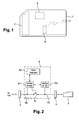
- the figure 1 shows a preferred embodiment of an adapter according to the invention.
- the adapter 1 is here made in the format of an SD memory card.
- the adapter 1 comprises a first connector 2 in the format of an SD card connector.
- the adapter 1 comprises a housing for receiving a memory card 3 in microSD format which is connected via a second connector 4.
- the adapter 1 comprises a chip 5 connected to the first and second connectors 2 and 4.
- the chip 5 contains the electronic circuits of the adapter 1.
- the electronic circuits of the adapter 1 are all placed on a single chip, however, it is possible to use circuits made on several chips.
- the figure 2 functionally details the electronic circuits contained in the chip 5.
- the first and second connectors 2 and 4 are connected to the chip, respectively by a first and a second bus 20 and 40 containing as many connectors as there are contacts for an SD card connector. For the sake of clarity of drawing, only one wire is shown.
- the first and second buses are interconnected via a first switch S1 which consists of a switch assembly for contacting or open circuit each conductor bus 20 and 40.
- the switch S1 allows either to ensure a direct connection between the two connectors 2 and 4, or to isolate them from one another.
- a device interface circuit 51 is connected to the first bus 20.
- the device interface circuit 51 is a circuit for communicating with a host connected to the first connector 2. It is the user interface circuit that provides the management of the communication protocol for an application circuit 52.
- the application circuit 52 may be of any type, for example an SD-MCE type pay television management circuit. Other application circuits are conceivable; the circuit 52 may be a modem having another connection, a chip card reader compliant with the ISO7816 standard, or any other type of application that can be connected by an SD bus.
- the device interface circuit 51 analyzes all the commands exchanged at the first connector 2. However, this interface circuit does not respond to all the commands. Indeed, some commands are processed directly by the card 3.
- the interface circuit is further connected to the switch S1 to control it and determine if the card responds directly or not, depending on the orders observed.
- a host interface circuit 53 is connected, on the one hand, to the second bus 40 and, on the other hand, to the device interface circuit 51.
- the host interface circuit 53 makes it possible to control the card 3 when the switch S1 is open.
- the link between the host interface circuit 53 is connected to the device interface circuit 51 to be able to integrate information from the card 3 to information returned by the device interface device 51.
- the adapter 1 is presented to the host that receives it as a single device integrating both the characteristics of the application circuit 52 and the characteristics of the card 3. During this start-up phase, the same principle that previously explained is implemented, however, it should also anticipate some control of the host device with respect to the card.
- the Vdd is chosen to correspond to both the card 3 and the adapter 1
- the maximum currents are added
- the transfer rates are determined as a function of the slower between the card and the device interface circuit 51, etc.
- the CSD and OCR registers are reconstituted to present characteristics which are compatible with both card 3 and adapter 1.
- the CID register it is also necessary to aggregate the data.
- the manufacturer of the adapter and the card are not the same.
- the card 3 is removable relative to the adapter and the identification information is not the same whether the card is present or not.
- the adapter must memorize this information because the address provided by the card can also be used to address the application circuit.
- the switching circuit 54 detects the command Cmd4 on the bus 20 and keeps the switch S1 closed.
- the interface circuit 51 does not respond and leaves switch S1 closed so that the card responds directly.
- the host interface circuit 53 intercepts the response and transmits the data or data to the circuit. device interface 51 for storage in the relevant register.
- the switch S1 is opened as soon as the completeness the order is placed.
- the host interface circuit receives the possible response from the card 3.
- the device interface circuit 51 will respond, possibly taking into account the response of the card 3.
- the device interface circuit 51 When the device interface circuit 51 has finished responding, it closes the card. S1 switch so that the card can receive the following command.
- the SD host When the SD host wants to send one or more commands to the application circuit 52, it must use an extended command set. For this it sends a command, for example Cmd6, which is not supported by the card 3.
- a command for example Cmd6, which is not supported by the card 3.
- the switching circuit 54 detects this command Cmd6, then it opens the switch S1.
- the card 3, having received the command Cmd6, can answer that it does not support this command but its answer is not transmitted to the host SD.
- the response is made by the interface circuit 51 and then the switch S1 is closed so that the card can receive the following command in case it is intended for it.
- the adapter In the event of a power failure, the adapter re-performs the start-up phase.
- the adapter without the card 3.
- the card will never respond to the commands that are sent. If we take the previous table, this results in no response to commands Cmd8 and Acmd41.
- the response to the command Cmd8 is optional and therefore does not mean the absence of the card.
- the absence of the OCR response within a specified time means that there is no card 3 and thus the device interface 51 can respond with its own OCR register immediately after the next Acmd41 command.
- the application circuit 52 it is possible for the application circuit 52 to store information on the card 3, in which case the switch S1 must be opened and the card 3 to be addressed with the aid of 53. If during this use of the card 3, the SD host sends a command to the card, the device interface circuit will respond that the card is not available using the "busy” response. ".
- An SDIO format card may have a larger portion than an SD card and it is possible to replace the microSD card 3 with any other SD or miniSD card format.
- the application circuit 52 can be of any type supported by the SDIO standard and it is possible that the application circuit 52 has a connection to another external circuit.
- the chip 5 corresponds to a set of electronic circuits made on a single chip. It is obvious that, depending on the type of application implemented by the adapter, the electronic circuits can be made on several separate chips.
Landscapes
- Engineering & Computer Science (AREA)
- Computer Hardware Design (AREA)
- Microelectronics & Electronic Packaging (AREA)
- Physics & Mathematics (AREA)
- General Physics & Mathematics (AREA)
- Theoretical Computer Science (AREA)
- Communication Control (AREA)
Priority Applications (6)
| Application Number | Priority Date | Filing Date | Title |
|---|---|---|---|
| EP08290660A EP2141706A1 (fr) | 2008-07-04 | 2008-07-04 | Adaptateur de carte mémoire |
| EP09772485A EP2304729B1 (en) | 2008-07-04 | 2009-07-01 | Memory card adapter |
| US13/001,387 US8602314B2 (en) | 2008-07-04 | 2009-07-01 | Memory card adapter |
| PCT/EP2009/058286 WO2010000785A1 (en) | 2008-07-04 | 2009-07-01 | Memory card adapter |
| JP2011515455A JP5501351B2 (ja) | 2008-07-04 | 2009-07-01 | メモリカードアダプタ |
| CN200980134094.9A CN102144262B (zh) | 2008-07-04 | 2009-07-01 | 存储卡适配器 |
Applications Claiming Priority (1)
| Application Number | Priority Date | Filing Date | Title |
|---|---|---|---|
| EP08290660A EP2141706A1 (fr) | 2008-07-04 | 2008-07-04 | Adaptateur de carte mémoire |
Publications (1)
| Publication Number | Publication Date |
|---|---|
| EP2141706A1 true EP2141706A1 (fr) | 2010-01-06 |
Family
ID=39817079
Family Applications (2)
| Application Number | Title | Priority Date | Filing Date |
|---|---|---|---|
| EP08290660A Withdrawn EP2141706A1 (fr) | 2008-07-04 | 2008-07-04 | Adaptateur de carte mémoire |
| EP09772485A Not-in-force EP2304729B1 (en) | 2008-07-04 | 2009-07-01 | Memory card adapter |
Family Applications After (1)
| Application Number | Title | Priority Date | Filing Date |
|---|---|---|---|
| EP09772485A Not-in-force EP2304729B1 (en) | 2008-07-04 | 2009-07-01 | Memory card adapter |
Country Status (5)
| Country | Link |
|---|---|
| US (1) | US8602314B2 (enExample) |
| EP (2) | EP2141706A1 (enExample) |
| JP (1) | JP5501351B2 (enExample) |
| CN (1) | CN102144262B (enExample) |
| WO (1) | WO2010000785A1 (enExample) |
Families Citing this family (4)
| Publication number | Priority date | Publication date | Assignee | Title |
|---|---|---|---|---|
| TWM423936U (en) * | 2011-09-13 | 2012-03-01 | Tyco Electronics Holdings Bermuda No 7 Ltd | Smartcard connector with RFID module |
| EP2711864A1 (en) * | 2012-09-25 | 2014-03-26 | Gemalto SA | Method of configuring two wireless devices for mutual communication |
| FR3038423B1 (fr) * | 2015-06-30 | 2018-07-20 | Idemia France | Entite electronique et procede mis en œuvre dans une telle entite electronique |
| TWI640870B (zh) * | 2017-03-17 | 2018-11-11 | 新唐科技股份有限公司 | 集線器 |
Citations (3)
| Publication number | Priority date | Publication date | Assignee | Title |
|---|---|---|---|---|
| US5936226A (en) * | 1995-09-27 | 1999-08-10 | Intel Corporation | Mass storage device adapter for smart cards |
| WO2002005102A1 (en) * | 2000-07-06 | 2002-01-17 | Onspec Electronic, Inc. | Flashtoaster for reading several types of flash memory cards with or without a pc |
| US20060164891A1 (en) * | 1999-05-11 | 2006-07-27 | Socket Communications, Inc. | Removable modules with external I/O flexibility via an integral second-level removable slot |
Family Cites Families (6)
| Publication number | Priority date | Publication date | Assignee | Title |
|---|---|---|---|---|
| JP3953832B2 (ja) | 2002-02-22 | 2007-08-08 | 株式会社村田製作所 | メディア媒体用インタフェースカード |
| JP3815400B2 (ja) * | 2002-08-08 | 2006-08-30 | ソニー株式会社 | アダプタ装置 |
| WO2005066745A1 (ja) | 2004-01-06 | 2005-07-21 | C-Guys, Inc. | バスシェアーアダプター |
| US20070132733A1 (en) * | 2004-06-08 | 2007-06-14 | Pranil Ram | Computer Apparatus with added functionality |
| US20070001017A1 (en) * | 2005-06-29 | 2007-01-04 | Moshe Nuri | Reduced complexity multifunction expansion card and method of operating the same |
| JP4640451B2 (ja) * | 2008-06-06 | 2011-03-02 | ソニー株式会社 | 接触・非接触複合icカード、通信方法、プログラム及び通信システム |
-
2008
- 2008-07-04 EP EP08290660A patent/EP2141706A1/fr not_active Withdrawn
-
2009
- 2009-07-01 CN CN200980134094.9A patent/CN102144262B/zh not_active Expired - Fee Related
- 2009-07-01 US US13/001,387 patent/US8602314B2/en not_active Expired - Fee Related
- 2009-07-01 EP EP09772485A patent/EP2304729B1/en not_active Not-in-force
- 2009-07-01 WO PCT/EP2009/058286 patent/WO2010000785A1/en not_active Ceased
- 2009-07-01 JP JP2011515455A patent/JP5501351B2/ja not_active Expired - Fee Related
Patent Citations (3)
| Publication number | Priority date | Publication date | Assignee | Title |
|---|---|---|---|---|
| US5936226A (en) * | 1995-09-27 | 1999-08-10 | Intel Corporation | Mass storage device adapter for smart cards |
| US20060164891A1 (en) * | 1999-05-11 | 2006-07-27 | Socket Communications, Inc. | Removable modules with external I/O flexibility via an integral second-level removable slot |
| WO2002005102A1 (en) * | 2000-07-06 | 2002-01-17 | Onspec Electronic, Inc. | Flashtoaster for reading several types of flash memory cards with or without a pc |
Also Published As
| Publication number | Publication date |
|---|---|
| US8602314B2 (en) | 2013-12-10 |
| EP2304729B1 (en) | 2012-09-05 |
| US20110201233A1 (en) | 2011-08-18 |
| JP5501351B2 (ja) | 2014-05-21 |
| CN102144262B (zh) | 2014-05-21 |
| WO2010000785A1 (en) | 2010-01-07 |
| CN102144262A (zh) | 2011-08-03 |
| EP2304729A1 (en) | 2011-04-06 |
| JP2011526713A (ja) | 2011-10-13 |
Similar Documents
| Publication | Publication Date | Title |
|---|---|---|
| EP1855229B1 (fr) | Procédé de routage de données sortantes et entrantes dans un chipset NFC | |
| EP2219353B1 (fr) | Téléphone portable incluant une batterie et un module de communication à champ proche | |
| US20050210195A1 (en) | System, apparatus and method for sharing media | |
| EP2251986A1 (en) | A near field communication device | |
| EP2172877A1 (fr) | Dispositif électronique et gestion de communication sans fils contribuant à un tel dispositif et un équipement hôte | |
| EP3716118B1 (fr) | Système électronique | |
| FR2987477A1 (fr) | Memoire non volatile pour routeur nfc | |
| EP2141706A1 (fr) | Adaptateur de carte mémoire | |
| EP3716117B1 (fr) | Système électronique | |
| EP3716130B1 (fr) | Système électronique | |
| FR2901077A1 (fr) | Procede de routage de donnees entrantes et sortantes dans un jeu de puces nfc | |
| WO2014023247A1 (zh) | 嵌入式设备和基于该设备进行数据通信的控制方法 | |
| EP3910974B1 (fr) | Module d'identification d'abonné et dispositif électronique | |
| EP2207131A1 (fr) | Carte à mémoire munie d'un microcontrôleur personnalisé | |
| FR2948794A1 (fr) | Carte a microcircuit comprenant au moins deux interfaces externes de contacts | |
| EP2579187A1 (fr) | Dispositif à microcircuit équipé de plages de contact et procédé de fabrication d'un tel dispositif | |
| CN100422973C (zh) | 基于单芯片的双界面控制器 | |
| WO2002058004A1 (fr) | Interconnexion de micromodules de cartes a puce et dispositif electronique portable comprenant une pluralite de micromodules de cartes a puce, connectes en reseau | |
| FR2991842A1 (fr) | Interface commune pour peripherique wifi et carte a puce | |
| WO2005124656A1 (fr) | Procede et systeme de communication haut debit a contacts electriques | |
| FR2996661A1 (fr) | Interface de telecommande pour lecteur de cartes a puces | |
| EP2725526A1 (fr) | Carte à puce comprenant un lecteur de carte USB intégré | |
| FR2901076A1 (fr) | Procede de routage de donnees sortantes et entrantes dans un chipset nfc | |
| FR2942582A1 (fr) | Dispositif portable, notamment du type cle usb, pourvu de plusieurs interfaces de communication sans contact selectionnables |
Legal Events
| Date | Code | Title | Description |
|---|---|---|---|
| PUAI | Public reference made under article 153(3) epc to a published international application that has entered the european phase |
Free format text: ORIGINAL CODE: 0009012 |
|
| AK | Designated contracting states |
Kind code of ref document: A1 Designated state(s): AT BE BG CH CY CZ DE DK EE ES FI FR GB GR HR HU IE IS IT LI LT LU LV MC MT NL NO PL PT RO SE SI SK TR |
|
| AX | Request for extension of the european patent |
Extension state: AL BA MK RS |
|
| AKY | No designation fees paid | ||
| REG | Reference to a national code |
Ref country code: DE Ref legal event code: 8566 |
|
| STAA | Information on the status of an ep patent application or granted ep patent |
Free format text: STATUS: THE APPLICATION IS DEEMED TO BE WITHDRAWN |
|
| 18D | Application deemed to be withdrawn |
Effective date: 20100707 |