EP2141190A1 - Barrier laminate, gas barrier film, device and method for producing barrier laminate - Google Patents
Barrier laminate, gas barrier film, device and method for producing barrier laminate Download PDFInfo
- Publication number
- EP2141190A1 EP2141190A1 EP20090008445 EP09008445A EP2141190A1 EP 2141190 A1 EP2141190 A1 EP 2141190A1 EP 20090008445 EP20090008445 EP 20090008445 EP 09008445 A EP09008445 A EP 09008445A EP 2141190 A1 EP2141190 A1 EP 2141190A1
- Authority
- EP
- European Patent Office
- Prior art keywords
- group
- barrier laminate
- layer
- film
- meth
- Prior art date
- Legal status (The legal status is an assumption and is not a legal conclusion. Google has not performed a legal analysis and makes no representation as to the accuracy of the status listed.)
- Granted
Links
- 230000004888 barrier function Effects 0.000 title claims abstract description 154
- 238000004519 manufacturing process Methods 0.000 title claims description 5
- 239000010410 layer Substances 0.000 claims abstract description 110
- 239000012044 organic layer Substances 0.000 claims abstract description 53
- NIXOWILDQLNWCW-UHFFFAOYSA-M Acrylate Chemical compound [O-]C(=O)C=C NIXOWILDQLNWCW-UHFFFAOYSA-M 0.000 claims abstract description 42
- 239000000203 mixture Substances 0.000 claims abstract description 26
- -1 acryloyloxy group Chemical group 0.000 claims description 41
- 239000000758 substrate Substances 0.000 claims description 37
- 238000000034 method Methods 0.000 claims description 32
- 150000001875 compounds Chemical class 0.000 claims description 25
- 125000001424 substituent group Chemical group 0.000 claims description 17
- 125000000524 functional group Chemical group 0.000 claims description 16
- 229910052751 metal Inorganic materials 0.000 claims description 15
- 239000002184 metal Substances 0.000 claims description 15
- 229910052782 aluminium Inorganic materials 0.000 claims description 9
- 150000004767 nitrides Chemical class 0.000 claims description 8
- 229910052710 silicon Inorganic materials 0.000 claims description 7
- 239000004411 aluminium Substances 0.000 claims description 6
- XAGFODPZIPBFFR-UHFFFAOYSA-N aluminium Chemical compound [Al] XAGFODPZIPBFFR-UHFFFAOYSA-N 0.000 claims description 6
- 238000004544 sputter deposition Methods 0.000 claims description 5
- 239000010703 silicon Substances 0.000 claims description 4
- 229910044991 metal oxide Inorganic materials 0.000 claims description 3
- 150000004706 metal oxides Chemical class 0.000 claims description 3
- 230000008569 process Effects 0.000 claims description 2
- 239000010408 film Substances 0.000 description 110
- 239000007789 gas Substances 0.000 description 66
- 239000000178 monomer Substances 0.000 description 18
- 230000015572 biosynthetic process Effects 0.000 description 15
- 239000000463 material Substances 0.000 description 12
- 238000006116 polymerization reaction Methods 0.000 description 11
- 125000000217 alkyl group Chemical group 0.000 description 10
- QVGXLLKOCUKJST-UHFFFAOYSA-N atomic oxygen Chemical compound [O] QVGXLLKOCUKJST-UHFFFAOYSA-N 0.000 description 10
- 229910052760 oxygen Inorganic materials 0.000 description 10
- 239000001301 oxygen Substances 0.000 description 10
- 239000002985 plastic film Substances 0.000 description 10
- 229920006255 plastic film Polymers 0.000 description 10
- 125000005647 linker group Chemical group 0.000 description 9
- 229920005989 resin Polymers 0.000 description 9
- 239000011347 resin Substances 0.000 description 9
- XLYOFNOQVPJJNP-UHFFFAOYSA-N water Substances O XLYOFNOQVPJJNP-UHFFFAOYSA-N 0.000 description 9
- 150000001252 acrylic acid derivatives Chemical class 0.000 description 8
- 229910052738 indium Inorganic materials 0.000 description 8
- 239000002346 layers by function Substances 0.000 description 8
- 125000003118 aryl group Chemical group 0.000 description 7
- 229910052802 copper Inorganic materials 0.000 description 7
- 239000010949 copper Substances 0.000 description 7
- 239000004973 liquid crystal related substance Substances 0.000 description 7
- 230000035699 permeability Effects 0.000 description 7
- 239000004417 polycarbonate Substances 0.000 description 7
- 238000007789 sealing Methods 0.000 description 7
- 239000000126 substance Substances 0.000 description 7
- 238000002834 transmittance Methods 0.000 description 7
- RYGMFSIKBFXOCR-UHFFFAOYSA-N Copper Chemical compound [Cu] RYGMFSIKBFXOCR-UHFFFAOYSA-N 0.000 description 6
- MWUXSHHQAYIFBG-UHFFFAOYSA-N Nitric oxide Chemical compound O=[N] MWUXSHHQAYIFBG-UHFFFAOYSA-N 0.000 description 6
- BUGBHKTXTAQXES-UHFFFAOYSA-N Selenium Chemical compound [Se] BUGBHKTXTAQXES-UHFFFAOYSA-N 0.000 description 6
- NIHNNTQXNPWCJQ-UHFFFAOYSA-N fluorene Chemical compound C1=CC=C2CC3=CC=CC=C3C2=C1 NIHNNTQXNPWCJQ-UHFFFAOYSA-N 0.000 description 6
- APFVFJFRJDLVQX-UHFFFAOYSA-N indium atom Chemical compound [In] APFVFJFRJDLVQX-UHFFFAOYSA-N 0.000 description 6
- 125000002467 phosphate group Chemical group [H]OP(=O)(O[H])O[*] 0.000 description 6
- 229910052711 selenium Inorganic materials 0.000 description 6
- 239000011669 selenium Substances 0.000 description 6
- GYHNNYVSQQEPJS-UHFFFAOYSA-N Gallium Chemical compound [Ga] GYHNNYVSQQEPJS-UHFFFAOYSA-N 0.000 description 4
- 239000004642 Polyimide Substances 0.000 description 4
- 230000002378 acidificating effect Effects 0.000 description 4
- 239000012790 adhesive layer Substances 0.000 description 4
- 238000000576 coating method Methods 0.000 description 4
- 238000010276 construction Methods 0.000 description 4
- 229920001577 copolymer Polymers 0.000 description 4
- 229910052733 gallium Inorganic materials 0.000 description 4
- 125000004435 hydrogen atom Chemical group [H]* 0.000 description 4
- 230000003287 optical effect Effects 0.000 description 4
- 239000002245 particle Substances 0.000 description 4
- 229920003207 poly(ethylene-2,6-naphthalate) Polymers 0.000 description 4
- 229920000515 polycarbonate Polymers 0.000 description 4
- 239000011112 polyethylene naphthalate Substances 0.000 description 4
- 229920001721 polyimide Polymers 0.000 description 4
- 239000003505 polymerization initiator Substances 0.000 description 4
- 239000004065 semiconductor Substances 0.000 description 4
- 239000000243 solution Substances 0.000 description 4
- 239000010409 thin film Substances 0.000 description 4
- PNEYBMLMFCGWSK-UHFFFAOYSA-N Alumina Chemical compound [O-2].[O-2].[O-2].[Al+3].[Al+3] PNEYBMLMFCGWSK-UHFFFAOYSA-N 0.000 description 3
- IJGRMHOSHXDMSA-UHFFFAOYSA-N Atomic nitrogen Chemical compound N#N IJGRMHOSHXDMSA-UHFFFAOYSA-N 0.000 description 3
- KFZMGEQAYNKOFK-UHFFFAOYSA-N Isopropanol Chemical compound CC(C)O KFZMGEQAYNKOFK-UHFFFAOYSA-N 0.000 description 3
- 125000003647 acryloyl group Chemical group O=C([*])C([H])=C([H])[H] 0.000 description 3
- 239000000853 adhesive Substances 0.000 description 3
- 230000001070 adhesive effect Effects 0.000 description 3
- 125000002723 alicyclic group Chemical group 0.000 description 3
- 125000003545 alkoxy group Chemical group 0.000 description 3
- 125000002947 alkylene group Chemical group 0.000 description 3
- 238000005229 chemical vapour deposition Methods 0.000 description 3
- ZUOUZKKEUPVFJK-UHFFFAOYSA-N diphenyl Chemical group C1=CC=CC=C1C1=CC=CC=C1 ZUOUZKKEUPVFJK-UHFFFAOYSA-N 0.000 description 3
- QSHDDOUJBYECFT-UHFFFAOYSA-N mercury Chemical compound [Hg] QSHDDOUJBYECFT-UHFFFAOYSA-N 0.000 description 3
- 229910052753 mercury Inorganic materials 0.000 description 3
- 125000001624 naphthyl group Chemical group 0.000 description 3
- 229910052757 nitrogen Inorganic materials 0.000 description 3
- 239000008188 pellet Substances 0.000 description 3
- 229920001230 polyarylate Polymers 0.000 description 3
- 229920005668 polycarbonate resin Polymers 0.000 description 3
- 239000004431 polycarbonate resin Substances 0.000 description 3
- 239000011241 protective layer Substances 0.000 description 3
- 230000005855 radiation Effects 0.000 description 3
- 229910052717 sulfur Inorganic materials 0.000 description 3
- 238000007740 vapor deposition Methods 0.000 description 3
- ZWEHNKRNPOVVGH-UHFFFAOYSA-N 2-Butanone Chemical compound CCC(C)=O ZWEHNKRNPOVVGH-UHFFFAOYSA-N 0.000 description 2
- LWRBVKNFOYUCNP-UHFFFAOYSA-N 2-methyl-1-(4-methylsulfanylphenyl)-2-morpholin-4-ylpropan-1-one Chemical compound C1=CC(SC)=CC=C1C(=O)C(C)(C)N1CCOCC1 LWRBVKNFOYUCNP-UHFFFAOYSA-N 0.000 description 2
- XKRFYHLGVUSROY-UHFFFAOYSA-N Argon Chemical compound [Ar] XKRFYHLGVUSROY-UHFFFAOYSA-N 0.000 description 2
- JBRZTFJDHDCESZ-UHFFFAOYSA-N AsGa Chemical compound [As]#[Ga] JBRZTFJDHDCESZ-UHFFFAOYSA-N 0.000 description 2
- OKTJSMMVPCPJKN-UHFFFAOYSA-N Carbon Chemical compound [C] OKTJSMMVPCPJKN-UHFFFAOYSA-N 0.000 description 2
- 229920000089 Cyclic olefin copolymer Polymers 0.000 description 2
- CBENFWSGALASAD-UHFFFAOYSA-N Ozone Chemical compound [O-][O+]=O CBENFWSGALASAD-UHFFFAOYSA-N 0.000 description 2
- XUIMIQQOPSSXEZ-UHFFFAOYSA-N Silicon Chemical compound [Si] XUIMIQQOPSSXEZ-UHFFFAOYSA-N 0.000 description 2
- NINIDFKCEFEMDL-UHFFFAOYSA-N Sulfur Chemical compound [S] NINIDFKCEFEMDL-UHFFFAOYSA-N 0.000 description 2
- 125000000732 arylene group Chemical group 0.000 description 2
- 125000004104 aryloxy group Chemical group 0.000 description 2
- 230000001588 bifunctional effect Effects 0.000 description 2
- RPPBZEBXAAZZJH-UHFFFAOYSA-N cadmium telluride Chemical compound [Te]=[Cd] RPPBZEBXAAZZJH-UHFFFAOYSA-N 0.000 description 2
- 239000011575 calcium Substances 0.000 description 2
- 239000002775 capsule Substances 0.000 description 2
- 229910052799 carbon Inorganic materials 0.000 description 2
- 125000005586 carbonic acid group Chemical group 0.000 description 2
- TXKMVPPZCYKFAC-UHFFFAOYSA-N disulfur monoxide Inorganic materials O=S=S TXKMVPPZCYKFAC-UHFFFAOYSA-N 0.000 description 2
- 125000001495 ethyl group Chemical group [H]C([H])([H])C([H])([H])* 0.000 description 2
- 125000000623 heterocyclic group Chemical group 0.000 description 2
- 239000003999 initiator Substances 0.000 description 2
- 238000007733 ion plating Methods 0.000 description 2
- PQXKHYXIUOZZFA-UHFFFAOYSA-M lithium fluoride Chemical compound [Li+].[F-] PQXKHYXIUOZZFA-UHFFFAOYSA-M 0.000 description 2
- 238000005259 measurement Methods 0.000 description 2
- 150000001247 metal acetylides Chemical class 0.000 description 2
- 125000002496 methyl group Chemical group [H]C([H])([H])* 0.000 description 2
- 125000001997 phenyl group Chemical group [H]C1=C([H])C([H])=C(*)C([H])=C1[H] 0.000 description 2
- 238000005240 physical vapour deposition Methods 0.000 description 2
- 238000005268 plasma chemical vapour deposition Methods 0.000 description 2
- 229920002492 poly(sulfone) Polymers 0.000 description 2
- 229920000728 polyester Polymers 0.000 description 2
- 229920001225 polyester resin Polymers 0.000 description 2
- 239000004645 polyester resin Substances 0.000 description 2
- 229920000642 polymer Polymers 0.000 description 2
- 230000000379 polymerizing effect Effects 0.000 description 2
- 229920000098 polyolefin Polymers 0.000 description 2
- 230000009467 reduction Effects 0.000 description 2
- 239000007787 solid Substances 0.000 description 2
- 125000000472 sulfonyl group Chemical group *S(*)(=O)=O 0.000 description 2
- 239000011593 sulfur Substances 0.000 description 2
- XTQHKBHJIVJGKJ-UHFFFAOYSA-N sulfur monoxide Chemical compound S=O XTQHKBHJIVJGKJ-UHFFFAOYSA-N 0.000 description 2
- 238000012360 testing method Methods 0.000 description 2
- 229920005992 thermoplastic resin Polymers 0.000 description 2
- 229920001187 thermosetting polymer Polymers 0.000 description 2
- 229910052718 tin Inorganic materials 0.000 description 2
- 229910052719 titanium Inorganic materials 0.000 description 2
- 229910001868 water Inorganic materials 0.000 description 2
- 229910052725 zinc Inorganic materials 0.000 description 2
- QNODIIQQMGDSEF-UHFFFAOYSA-N (1-hydroxycyclohexyl)-phenylmethanone Chemical compound C=1C=CC=CC=1C(=O)C1(O)CCCCC1 QNODIIQQMGDSEF-UHFFFAOYSA-N 0.000 description 1
- ODIGIKRIUKFKHP-UHFFFAOYSA-N (n-propan-2-yloxycarbonylanilino) acetate Chemical compound CC(C)OC(=O)N(OC(C)=O)C1=CC=CC=C1 ODIGIKRIUKFKHP-UHFFFAOYSA-N 0.000 description 1
- WKBPZYKAUNRMKP-UHFFFAOYSA-N 1-[2-(2,4-dichlorophenyl)pentyl]1,2,4-triazole Chemical compound C=1C=C(Cl)C=C(Cl)C=1C(CCC)CN1C=NC=N1 WKBPZYKAUNRMKP-UHFFFAOYSA-N 0.000 description 1
- PZNGVDGOACAMOQ-UHFFFAOYSA-N 1-ethenoxyprop-1-yne Chemical group CC#COC=C PZNGVDGOACAMOQ-UHFFFAOYSA-N 0.000 description 1
- 125000001637 1-naphthyl group Chemical group [H]C1=C([H])C([H])=C2C(*)=C([H])C([H])=C([H])C2=C1[H] 0.000 description 1
- KWVGIHKZDCUPEU-UHFFFAOYSA-N 2,2-dimethoxy-2-phenylacetophenone Chemical compound C=1C=CC=CC=1C(OC)(OC)C(=O)C1=CC=CC=C1 KWVGIHKZDCUPEU-UHFFFAOYSA-N 0.000 description 1
- YQTCQNIPQMJNTI-UHFFFAOYSA-N 2,2-dimethylpropan-1-one Chemical group CC(C)(C)[C]=O YQTCQNIPQMJNTI-UHFFFAOYSA-N 0.000 description 1
- GJKGAPPUXSSCFI-UHFFFAOYSA-N 2-Hydroxy-4'-(2-hydroxyethoxy)-2-methylpropiophenone Chemical compound CC(C)(O)C(=O)C1=CC=C(OCCO)C=C1 GJKGAPPUXSSCFI-UHFFFAOYSA-N 0.000 description 1
- FIOCEWASVZHBTK-UHFFFAOYSA-N 2-[2-(2-oxo-2-phenylacetyl)oxyethoxy]ethyl 2-oxo-2-phenylacetate Chemical compound C=1C=CC=CC=1C(=O)C(=O)OCCOCCOC(=O)C(=O)C1=CC=CC=C1 FIOCEWASVZHBTK-UHFFFAOYSA-N 0.000 description 1
- UHFFVFAKEGKNAQ-UHFFFAOYSA-N 2-benzyl-2-(dimethylamino)-1-(4-morpholin-4-ylphenyl)butan-1-one Chemical compound C=1C=C(N2CCOCC2)C=CC=1C(=O)C(CC)(N(C)C)CC1=CC=CC=C1 UHFFVFAKEGKNAQ-UHFFFAOYSA-N 0.000 description 1
- 125000004974 2-butenyl group Chemical group C(C=CC)* 0.000 description 1
- XMLYCEVDHLAQEL-UHFFFAOYSA-N 2-hydroxy-2-methyl-1-phenylpropan-1-one Chemical compound CC(C)(O)C(=O)C1=CC=CC=C1 XMLYCEVDHLAQEL-UHFFFAOYSA-N 0.000 description 1
- 125000003903 2-propenyl group Chemical group [H]C([*])([H])C([H])=C([H])[H] 0.000 description 1
- 125000000590 4-methylphenyl group Chemical group [H]C1=C([H])C(=C([H])C([H])=C1*)C([H])([H])[H] 0.000 description 1
- ZCYVEMRRCGMTRW-UHFFFAOYSA-N 7553-56-2 Chemical group [I] ZCYVEMRRCGMTRW-UHFFFAOYSA-N 0.000 description 1
- 239000004925 Acrylic resin Substances 0.000 description 1
- 229920002799 BoPET Polymers 0.000 description 1
- WKBOTKDWSSQWDR-UHFFFAOYSA-N Bromine atom Chemical group [Br] WKBOTKDWSSQWDR-UHFFFAOYSA-N 0.000 description 1
- OYPRJOBELJOOCE-UHFFFAOYSA-N Calcium Chemical compound [Ca] OYPRJOBELJOOCE-UHFFFAOYSA-N 0.000 description 1
- 229920002284 Cellulose triacetate Polymers 0.000 description 1
- 229910052684 Cerium Inorganic materials 0.000 description 1
- 239000004593 Epoxy Substances 0.000 description 1
- JOYRKODLDBILNP-UHFFFAOYSA-N Ethyl urethane Chemical compound CCOC(N)=O JOYRKODLDBILNP-UHFFFAOYSA-N 0.000 description 1
- GPXJNWSHGFTCBW-UHFFFAOYSA-N Indium phosphide Chemical compound [In]#P GPXJNWSHGFTCBW-UHFFFAOYSA-N 0.000 description 1
- 229920000106 Liquid crystal polymer Polymers 0.000 description 1
- 239000004977 Liquid-crystal polymers (LCPs) Substances 0.000 description 1
- CERQOIWHTDAKMF-UHFFFAOYSA-M Methacrylate Chemical compound CC(=C)C([O-])=O CERQOIWHTDAKMF-UHFFFAOYSA-M 0.000 description 1
- 239000004696 Poly ether ether ketone Substances 0.000 description 1
- 229920012266 Poly(ether sulfone) PES Polymers 0.000 description 1
- 239000004695 Polyether sulfone Substances 0.000 description 1
- 239000004697 Polyetherimide Substances 0.000 description 1
- 229910052581 Si3N4 Inorganic materials 0.000 description 1
- NNLVGZFZQQXQNW-ADJNRHBOSA-N [(2r,3r,4s,5r,6s)-4,5-diacetyloxy-3-[(2s,3r,4s,5r,6r)-3,4,5-triacetyloxy-6-(acetyloxymethyl)oxan-2-yl]oxy-6-[(2r,3r,4s,5r,6s)-4,5,6-triacetyloxy-2-(acetyloxymethyl)oxan-3-yl]oxyoxan-2-yl]methyl acetate Chemical compound O([C@@H]1O[C@@H]([C@H]([C@H](OC(C)=O)[C@H]1OC(C)=O)O[C@H]1[C@@H]([C@@H](OC(C)=O)[C@H](OC(C)=O)[C@@H](COC(C)=O)O1)OC(C)=O)COC(=O)C)[C@@H]1[C@@H](COC(C)=O)O[C@@H](OC(C)=O)[C@H](OC(C)=O)[C@H]1OC(C)=O NNLVGZFZQQXQNW-ADJNRHBOSA-N 0.000 description 1
- 238000010521 absorption reaction Methods 0.000 description 1
- 125000004054 acenaphthylenyl group Chemical group C1(=CC2=CC=CC3=CC=CC1=C23)* 0.000 description 1
- 239000004480 active ingredient Substances 0.000 description 1
- 125000002252 acyl group Chemical group 0.000 description 1
- 239000000654 additive Substances 0.000 description 1
- 238000007754 air knife coating Methods 0.000 description 1
- 125000001931 aliphatic group Chemical group 0.000 description 1
- 125000003342 alkenyl group Chemical group 0.000 description 1
- 125000004453 alkoxycarbonyl group Chemical group 0.000 description 1
- 229910021417 amorphous silicon Inorganic materials 0.000 description 1
- 125000005577 anthracene group Chemical group 0.000 description 1
- 125000005428 anthryl group Chemical group [H]C1=C([H])C([H])=C2C([H])=C3C(*)=C([H])C([H])=C([H])C3=C([H])C2=C1[H] 0.000 description 1
- 101150059062 apln gene Proteins 0.000 description 1
- 229910052786 argon Inorganic materials 0.000 description 1
- 125000005161 aryl oxy carbonyl group Chemical group 0.000 description 1
- 125000002785 azepinyl group Chemical group 0.000 description 1
- 125000003828 azulenyl group Chemical group 0.000 description 1
- 238000007611 bar coating method Methods 0.000 description 1
- 125000003785 benzimidazolyl group Chemical group N1=C(NC2=C1C=CC=C2)* 0.000 description 1
- TXVHTIQJNYSSKO-UHFFFAOYSA-N benzo[e]pyrene Chemical group C1=CC=C2C3=CC=CC=C3C3=CC=CC4=CC=C1C2=C34 TXVHTIQJNYSSKO-UHFFFAOYSA-N 0.000 description 1
- 125000001164 benzothiazolyl group Chemical group S1C(=NC2=C1C=CC=C2)* 0.000 description 1
- 125000004541 benzoxazolyl group Chemical group O1C(=NC2=C1C=CC=C2)* 0.000 description 1
- 125000003236 benzoyl group Chemical group [H]C1=C([H])C([H])=C(C([H])=C1[H])C(*)=O 0.000 description 1
- ZDZHCHYQNPQSGG-UHFFFAOYSA-N binaphthyl group Chemical group C1(=CC=CC2=CC=CC=C12)C1=CC=CC2=CC=CC=C12 ZDZHCHYQNPQSGG-UHFFFAOYSA-N 0.000 description 1
- 235000010290 biphenyl Nutrition 0.000 description 1
- 239000004305 biphenyl Substances 0.000 description 1
- 125000002529 biphenylenyl group Chemical group C1(=CC=CC=2C3=CC=CC=C3C12)* 0.000 description 1
- 125000000484 butyl group Chemical group [H]C([*])([H])C([H])([H])C([H])([H])C([H])([H])[H] 0.000 description 1
- 229910052791 calcium Inorganic materials 0.000 description 1
- 125000000609 carbazolyl group Chemical group C1(=CC=CC=2C3=CC=CC=C3NC12)* 0.000 description 1
- 125000004432 carbon atom Chemical group C* 0.000 description 1
- 125000002915 carbonyl group Chemical group [*:2]C([*:1])=O 0.000 description 1
- 229920002678 cellulose Polymers 0.000 description 1
- 239000001913 cellulose Substances 0.000 description 1
- 230000008859 change Effects 0.000 description 1
- 238000006243 chemical reaction Methods 0.000 description 1
- 229910052801 chlorine Inorganic materials 0.000 description 1
- 125000001309 chloro group Chemical group Cl* 0.000 description 1
- 125000005578 chrysene group Chemical group 0.000 description 1
- 239000011248 coating agent Substances 0.000 description 1
- 230000001447 compensatory effect Effects 0.000 description 1
- JNGZXGGOCLZBFB-IVCQMTBJSA-N compound E Chemical compound N([C@@H](C)C(=O)N[C@@H]1C(N(C)C2=CC=CC=C2C(C=2C=CC=CC=2)=N1)=O)C(=O)CC1=CC(F)=CC(F)=C1 JNGZXGGOCLZBFB-IVCQMTBJSA-N 0.000 description 1
- 238000007766 curtain coating Methods 0.000 description 1
- 125000004122 cyclic group Chemical group 0.000 description 1
- 125000000113 cyclohexyl group Chemical group [H]C1([H])C([H])([H])C([H])([H])C([H])(*)C([H])([H])C1([H])[H] 0.000 description 1
- 125000001511 cyclopentyl group Chemical group [H]C1([H])C([H])([H])C([H])([H])C([H])(*)C1([H])[H] 0.000 description 1
- 125000001559 cyclopropyl group Chemical group [H]C1([H])C([H])([H])C1([H])* 0.000 description 1
- 238000007598 dipping method Methods 0.000 description 1
- 230000000694 effects Effects 0.000 description 1
- 238000005516 engineering process Methods 0.000 description 1
- 239000003822 epoxy resin Substances 0.000 description 1
- LZWYWAIOTBEZFN-UHFFFAOYSA-N ethenyl hexanoate Chemical group CCCCCC(=O)OC=C LZWYWAIOTBEZFN-UHFFFAOYSA-N 0.000 description 1
- 125000001033 ether group Chemical group 0.000 description 1
- 125000005677 ethinylene group Chemical group [*:2]C#C[*:1] 0.000 description 1
- 125000003754 ethoxycarbonyl group Chemical group C(=O)(OCC)* 0.000 description 1
- 238000011156 evaluation Methods 0.000 description 1
- 238000001704 evaporation Methods 0.000 description 1
- 238000007765 extrusion coating Methods 0.000 description 1
- 229910052731 fluorine Inorganic materials 0.000 description 1
- 125000001153 fluoro group Chemical group F* 0.000 description 1
- 125000002485 formyl group Chemical group [H]C(*)=O 0.000 description 1
- 125000002541 furyl group Chemical group 0.000 description 1
- 239000011521 glass Substances 0.000 description 1
- 230000009477 glass transition Effects 0.000 description 1
- 238000007756 gravure coating Methods 0.000 description 1
- 125000005843 halogen group Chemical group 0.000 description 1
- 239000003779 heat-resistant material Substances 0.000 description 1
- RBTKNAXYKSUFRK-UHFFFAOYSA-N heliogen blue Chemical compound [Cu].[N-]1C2=C(C=CC=C3)C3=C1N=C([N-]1)C3=CC=CC=C3C1=NC([N-]1)=C(C=CC=C3)C3=C1N=C([N-]1)C3=CC=CC=C3C1=N2 RBTKNAXYKSUFRK-UHFFFAOYSA-N 0.000 description 1
- 125000001072 heteroaryl group Chemical group 0.000 description 1
- 125000005842 heteroatom Chemical group 0.000 description 1
- 125000004051 hexyl group Chemical group [H]C([H])([H])C([H])([H])C([H])([H])C([H])([H])C([H])([H])C([H])([H])* 0.000 description 1
- 125000002883 imidazolyl group Chemical group 0.000 description 1
- 125000001841 imino group Chemical group [H]N=* 0.000 description 1
- 239000012535 impurity Substances 0.000 description 1
- 238000007373 indentation Methods 0.000 description 1
- 229910010272 inorganic material Inorganic materials 0.000 description 1
- 239000011147 inorganic material Substances 0.000 description 1
- 229910052740 iodine Inorganic materials 0.000 description 1
- 125000001449 isopropyl group Chemical group [H]C([H])([H])C([H])(*)C([H])([H])[H] 0.000 description 1
- 238000010030 laminating Methods 0.000 description 1
- 238000003475 lamination Methods 0.000 description 1
- 239000007791 liquid phase Substances 0.000 description 1
- 239000006224 matting agent Substances 0.000 description 1
- 238000000691 measurement method Methods 0.000 description 1
- 150000002736 metal compounds Chemical class 0.000 description 1
- 125000005641 methacryl group Chemical group 0.000 description 1
- 125000001160 methoxycarbonyl group Chemical group [H]C([H])([H])OC(*)=O 0.000 description 1
- 125000004170 methylsulfonyl group Chemical group [H]C([H])([H])S(*)(=O)=O 0.000 description 1
- 229910021421 monocrystalline silicon Inorganic materials 0.000 description 1
- 125000004573 morpholin-4-yl group Chemical group N1(CCOCC1)* 0.000 description 1
- IBHBKWKFFTZAHE-UHFFFAOYSA-N n-[4-[4-(n-naphthalen-1-ylanilino)phenyl]phenyl]-n-phenylnaphthalen-1-amine Chemical compound C1=CC=CC=C1N(C=1C2=CC=CC=C2C=CC=1)C1=CC=C(C=2C=CC(=CC=2)N(C=2C=CC=CC=2)C=2C3=CC=CC=C3C=CC=2)C=C1 IBHBKWKFFTZAHE-UHFFFAOYSA-N 0.000 description 1
- 125000004433 nitrogen atom Chemical group N* 0.000 description 1
- QJGQUHMNIGDVPM-UHFFFAOYSA-N nitrogen group Chemical group [N] QJGQUHMNIGDVPM-UHFFFAOYSA-N 0.000 description 1
- 150000002894 organic compounds Chemical class 0.000 description 1
- 125000004430 oxygen atom Chemical group O* 0.000 description 1
- 125000001147 pentyl group Chemical group C(CCCC)* 0.000 description 1
- 125000001792 phenanthrenyl group Chemical group C1(=CC=CC=2C3=CC=CC=C3C=CC12)* 0.000 description 1
- 125000005561 phenanthryl group Chemical group 0.000 description 1
- 125000000843 phenylene group Chemical group C1(=C(C=CC=C1)*)* 0.000 description 1
- 125000003170 phenylsulfonyl group Chemical group C1(=CC=CC=C1)S(=O)(=O)* 0.000 description 1
- 125000001388 picenyl group Chemical group C1(=CC=CC2=CC=C3C4=CC=C5C=CC=CC5=C4C=CC3=C21)* 0.000 description 1
- 125000005936 piperidyl group Chemical group 0.000 description 1
- 238000007747 plating Methods 0.000 description 1
- 229920002239 polyacrylonitrile Polymers 0.000 description 1
- 229920006122 polyamide resin Polymers 0.000 description 1
- 229920002312 polyamide-imide Polymers 0.000 description 1
- 229910021420 polycrystalline silicon Inorganic materials 0.000 description 1
- 229920000647 polyepoxide Polymers 0.000 description 1
- 229920006393 polyether sulfone Polymers 0.000 description 1
- 229920002530 polyetherether ketone Polymers 0.000 description 1
- 229920001601 polyetherimide Polymers 0.000 description 1
- 229920006290 polyethylene naphthalate film Polymers 0.000 description 1
- 229920005672 polyolefin resin Polymers 0.000 description 1
- 229920005990 polystyrene resin Polymers 0.000 description 1
- 229920005749 polyurethane resin Polymers 0.000 description 1
- 125000001436 propyl group Chemical group [H]C([*])([H])C([H])([H])C([H])([H])[H] 0.000 description 1
- LVTJOONKWUXEFR-FZRMHRINSA-N protoneodioscin Natural products O(C[C@@H](CC[C@]1(O)[C@H](C)[C@@H]2[C@]3(C)[C@H]([C@H]4[C@@H]([C@]5(C)C(=CC4)C[C@@H](O[C@@H]4[C@H](O[C@H]6[C@@H](O)[C@@H](O)[C@@H](O)[C@H](C)O6)[C@@H](O)[C@H](O[C@H]6[C@@H](O)[C@@H](O)[C@@H](O)[C@H](C)O6)[C@H](CO)O4)CC5)CC3)C[C@@H]2O1)C)[C@H]1[C@H](O)[C@H](O)[C@H](O)[C@@H](CO)O1 LVTJOONKWUXEFR-FZRMHRINSA-N 0.000 description 1
- 238000010926 purge Methods 0.000 description 1
- 125000005581 pyrene group Chemical group 0.000 description 1
- 125000001725 pyrenyl group Chemical group 0.000 description 1
- 125000004076 pyridyl group Chemical group 0.000 description 1
- 125000005493 quinolyl group Chemical group 0.000 description 1
- 239000012495 reaction gas Substances 0.000 description 1
- 230000002040 relaxant effect Effects 0.000 description 1
- 238000011160 research Methods 0.000 description 1
- 238000007761 roller coating Methods 0.000 description 1
- HQVNEWCFYHHQES-UHFFFAOYSA-N silicon nitride Chemical compound N12[Si]34N5[Si]62N3[Si]51N64 HQVNEWCFYHHQES-UHFFFAOYSA-N 0.000 description 1
- 238000007767 slide coating Methods 0.000 description 1
- 238000003980 solgel method Methods 0.000 description 1
- 238000009987 spinning Methods 0.000 description 1
- 238000006467 substitution reaction Methods 0.000 description 1
- 125000000475 sulfinyl group Chemical group [*:2]S([*:1])=O 0.000 description 1
- 125000004434 sulfur atom Chemical group 0.000 description 1
- 239000000725 suspension Substances 0.000 description 1
- 229910052715 tantalum Inorganic materials 0.000 description 1
- 125000000999 tert-butyl group Chemical group [H]C([H])([H])C(*)(C([H])([H])[H])C([H])([H])[H] 0.000 description 1
- 125000001544 thienyl group Chemical group 0.000 description 1
- 239000012780 transparent material Substances 0.000 description 1
- TVIVIEFSHFOWTE-UHFFFAOYSA-K tri(quinolin-8-yloxy)alumane Chemical compound [Al+3].C1=CN=C2C([O-])=CC=CC2=C1.C1=CN=C2C([O-])=CC=CC2=C1.C1=CN=C2C([O-])=CC=CC2=C1 TVIVIEFSHFOWTE-UHFFFAOYSA-K 0.000 description 1
- 125000005580 triphenylene group Chemical group 0.000 description 1
- 238000001771 vacuum deposition Methods 0.000 description 1
- 125000000391 vinyl group Chemical group [H]C([*])=C([H])[H] 0.000 description 1
Classifications
-
- C—CHEMISTRY; METALLURGY
- C08—ORGANIC MACROMOLECULAR COMPOUNDS; THEIR PREPARATION OR CHEMICAL WORKING-UP; COMPOSITIONS BASED THEREON
- C08J—WORKING-UP; GENERAL PROCESSES OF COMPOUNDING; AFTER-TREATMENT NOT COVERED BY SUBCLASSES C08B, C08C, C08F, C08G or C08H
- C08J7/00—Chemical treatment or coating of shaped articles made of macromolecular substances
- C08J7/04—Coating
- C08J7/042—Coating with two or more layers, where at least one layer of a composition contains a polymer binder
- C08J7/0423—Coating with two or more layers, where at least one layer of a composition contains a polymer binder with at least one layer of inorganic material and at least one layer of a composition containing a polymer binder
-
- C—CHEMISTRY; METALLURGY
- C08—ORGANIC MACROMOLECULAR COMPOUNDS; THEIR PREPARATION OR CHEMICAL WORKING-UP; COMPOSITIONS BASED THEREON
- C08J—WORKING-UP; GENERAL PROCESSES OF COMPOUNDING; AFTER-TREATMENT NOT COVERED BY SUBCLASSES C08B, C08C, C08F, C08G or C08H
- C08J7/00—Chemical treatment or coating of shaped articles made of macromolecular substances
- C08J7/04—Coating
- C08J7/043—Improving the adhesiveness of the coatings per se, e.g. forming primers
-
- C—CHEMISTRY; METALLURGY
- C08—ORGANIC MACROMOLECULAR COMPOUNDS; THEIR PREPARATION OR CHEMICAL WORKING-UP; COMPOSITIONS BASED THEREON
- C08J—WORKING-UP; GENERAL PROCESSES OF COMPOUNDING; AFTER-TREATMENT NOT COVERED BY SUBCLASSES C08B, C08C, C08F, C08G or C08H
- C08J7/00—Chemical treatment or coating of shaped articles made of macromolecular substances
- C08J7/04—Coating
- C08J7/048—Forming gas barrier coatings
-
- C—CHEMISTRY; METALLURGY
- C08—ORGANIC MACROMOLECULAR COMPOUNDS; THEIR PREPARATION OR CHEMICAL WORKING-UP; COMPOSITIONS BASED THEREON
- C08J—WORKING-UP; GENERAL PROCESSES OF COMPOUNDING; AFTER-TREATMENT NOT COVERED BY SUBCLASSES C08B, C08C, C08F, C08G or C08H
- C08J2333/00—Characterised by the use of homopolymers or copolymers of compounds having one or more unsaturated aliphatic radicals, each having only one carbon-to-carbon double bond, and only one being terminated by only one carboxyl radical, or of salts, anhydrides, esters, amides, imides, or nitriles thereof; Derivatives of such polymers
- C08J2333/04—Characterised by the use of homopolymers or copolymers of compounds having one or more unsaturated aliphatic radicals, each having only one carbon-to-carbon double bond, and only one being terminated by only one carboxyl radical, or of salts, anhydrides, esters, amides, imides, or nitriles thereof; Derivatives of such polymers esters
- C08J2333/06—Characterised by the use of homopolymers or copolymers of compounds having one or more unsaturated aliphatic radicals, each having only one carbon-to-carbon double bond, and only one being terminated by only one carboxyl radical, or of salts, anhydrides, esters, amides, imides, or nitriles thereof; Derivatives of such polymers esters of esters containing only carbon, hydrogen, and oxygen, the oxygen atom being present only as part of the carboxyl radical
-
- Y—GENERAL TAGGING OF NEW TECHNOLOGICAL DEVELOPMENTS; GENERAL TAGGING OF CROSS-SECTIONAL TECHNOLOGIES SPANNING OVER SEVERAL SECTIONS OF THE IPC; TECHNICAL SUBJECTS COVERED BY FORMER USPC CROSS-REFERENCE ART COLLECTIONS [XRACs] AND DIGESTS
- Y10—TECHNICAL SUBJECTS COVERED BY FORMER USPC
- Y10T—TECHNICAL SUBJECTS COVERED BY FORMER US CLASSIFICATION
- Y10T428/00—Stock material or miscellaneous articles
- Y10T428/31504—Composite [nonstructural laminate]
- Y10T428/31551—Of polyamidoester [polyurethane, polyisocyanate, polycarbamate, etc.]
- Y10T428/31645—Next to addition polymer from unsaturated monomers
- Y10T428/31649—Ester, halide or nitrile of addition polymer
-
- Y—GENERAL TAGGING OF NEW TECHNOLOGICAL DEVELOPMENTS; GENERAL TAGGING OF CROSS-SECTIONAL TECHNOLOGIES SPANNING OVER SEVERAL SECTIONS OF THE IPC; TECHNICAL SUBJECTS COVERED BY FORMER USPC CROSS-REFERENCE ART COLLECTIONS [XRACs] AND DIGESTS
- Y10—TECHNICAL SUBJECTS COVERED BY FORMER USPC
- Y10T—TECHNICAL SUBJECTS COVERED BY FORMER US CLASSIFICATION
- Y10T428/00—Stock material or miscellaneous articles
- Y10T428/31504—Composite [nonstructural laminate]
- Y10T428/31652—Of asbestos
- Y10T428/31667—Next to addition polymer from unsaturated monomers, or aldehyde or ketone condensation product
-
- Y—GENERAL TAGGING OF NEW TECHNOLOGICAL DEVELOPMENTS; GENERAL TAGGING OF CROSS-SECTIONAL TECHNOLOGIES SPANNING OVER SEVERAL SECTIONS OF THE IPC; TECHNICAL SUBJECTS COVERED BY FORMER USPC CROSS-REFERENCE ART COLLECTIONS [XRACs] AND DIGESTS
- Y10—TECHNICAL SUBJECTS COVERED BY FORMER USPC
- Y10T—TECHNICAL SUBJECTS COVERED BY FORMER US CLASSIFICATION
- Y10T428/00—Stock material or miscellaneous articles
- Y10T428/31504—Composite [nonstructural laminate]
- Y10T428/31855—Of addition polymer from unsaturated monomers
- Y10T428/31935—Ester, halide or nitrile of addition polymer
Definitions
- the present invention relates to a barrier laminate, a gas barrier film, and a device using the barrier laminate or the gas barrier film.
- the present invention also relates to a method for producing barrier laminate.
- JP-A-10-278167 discloses a barrier film having a planarizing layer comprising a cardo polymer.
- Demand of higher barrier property of a gas barrier film is increasing year after year.
- a gas barrier film used as a substrate of a device requires its surface smoothness.
- One object of the invention is to provide a barrier laminate having higher barrier property. Another object of the invention is to provide a barrier laminate having a planarized surface.
- the present invention provides a gas barrier film comprising the laminate.
- the present inventor has assiduously studied and, as a result, have found that the above object can be solved by using, as a material of an organic layer, a material obtained by curing a polymerizable composition comprising a (meth) acrylate having a polycyclic aromatic skeleton consisting of SP 2 carbon atoms. Specifically, he has found that the above objection can be solved by the following means.
- the present invention made it possible to provide a barrier laminate having enhanced barrier property.
- the barrier laminate of the present invention comprises at least one organic layer and at least one inorganic layer, preferably a structure of an inorganic layer on an organic layer, more preferably a structure in which at least two organic layers and at least two inorganic layers are laminated alternately.
- the barrier laminate of the present invention may contain a gradation material layer where an organic region and an inorganic region continuously change in the thickness direction of the laminate without diverting the scope of the present invention.
- a gradation material layer where an organic region and an inorganic region continuously change in the thickness direction of the laminate without diverting the scope of the present invention.
- the gradation material there are mentioned materials described in Kim et al's report, Journal of Vacuum Science and Technology A, Vol. 23 pp. 971-977 (2005 American Vacuum Society ); and gradation layers of an organic layer and an inorganic layer laminated with no boundary therebetween as in US Laid-Open 2004-46497 .
- the number of the layers that constitute the barrier laminate is typically preferably 2 to 30, more preferably 3 to 20.
- the barrier laminate of the present invention may comprise a layer other than an organic layer and an inorganic layer.
- At least one organic layer in the present invention is formed by curing a polymerizable composition comprising a (meth)acrylate having a polycyclic aromatic skeleton consisting of SP 2 carbon atoms.
- Examples of the polycyclic aromatic skeleton in the present invention include a biphenyl skeleton, a naphthalene skeleton, a binaphthyl skeleton, an azulene skeleton, a biphenylene skeleton, an acenaphthylene skeleton, a phenanthrene skeleton, an anthracene skeleton, a triphenylene skeleton, a pyrene skeleton, a chrysene skeleton, a napthacene skeleton, a picene skeleton, a pyrelyne skeleton, and a benzopyrene skeleton.
- the (meth) acrylate having a polycyclic aromatic skeleton consisting of SP 2 carbon atoms may have one or more functional groups, preferably two or more functional groups, still more preferably two functional groups.
- a (meth)acrylate having two or more functional groups By employing a (meth)acrylate having two or more functional groups , higher barrier property is achieved.
- the (meth)acrylaoyl group may directly bond to the polycyclic aromatic skeleton, or may bond to it via a linking group, preferably bond to it via a divalent linking group.
- divalent linking group examples include an alkylene group (for example, 1, 3-propylene group, 2, 2-dimethyl-1, 3-propylene group, 2-buthyl-2-ethyl-1, 3-propylene group, 1, 6-hexylene group, 1, 9-nonylene group, 1,12-dodecylene group, 1, 16-hexdecylene), an arylene group (for example, phenylene group and naphthalene group), an ether group, an imino group, a carbonyl group, a sulfonyl group, and a divalent residue formed by serially bonding plurality of those divalent linking groups (for example, polyethyleneoxy group, polypropyleneoxy group, propynyloxyethylene group, butyloyloxypropylene group, caproyloxyethylene group, caproyloxybutylene group, 2, 2-propilenephenylene group).
- alkylene group for example, 1, 3-propylene group, 2, 2-dimethyl-1, 3-propylene
- L 1 and L 2 may have a substituent.
- substituent which substitutes the linking group include an alkyl group (for example, methyl group, ethyl group, isopropyl group, t-butyl group, n-octyl group, n-decyl group, n-hexadecyl group, cyclopropyl group, cyclopentyl group, cyclohexyl group), an alkenyl group (for example, vinyl group, allyl group, 2-butenyl group, 3-pentenyl group), an aryl group (for example, phenyl group, p-methylphenyl group, naphthyl group, anthryl group, phenanthryl group and pyrenyl group), a halogen atom (for example, fluorine atom, chlorine atom, bromine atom and iodine atom), an acyl group (
- the (meth) acrylate having a polycyclic aromatic skeleton consisting of SP 2 carbon atoms may have a substituent without diverting the gist of the present invention.
- the molecular weight of the (meth)acrylate having a polycyclic aromatic skeleton consisting of SP 2 carbon atoms is preferably 100 to 1000, more preferably 200 to 500.
- the (meth) acrylate having a polycyclic aromatic skeleton consisting of SP 2 carbon atoms in the present invention is preferably represented by the following formula (1) or (2): wherein R 1 and R 2 each represent a substituent; m and n each are an integer of 0 to 5; when m is not less than 2, each R 1 may be the same or different, when n is not less than 2, each R 2 are the same or different; and a compound represented by the formula (1) or (2) has at least one acryloyloxy group or at least one methacryloyloxy group in the molecule.
- R 1 and R 2 as the substituent not having an acryloyloxy group and a methacryloyloxy group include an alkyl group, an aryl group, and an alkoxy group.
- the compound represented by the following formula (1) or (2) does not preferably include any substituent other than an acryloyloxy group and a methacryloyloxy group.
- the substituent having an acryloyloxy group or a methacryloyloxy group as R 1 and R 2 may be an acryloyloxy group or a methacryloyloxy group, preferably a group consisting of a divalent linking group and one of an acryloyloxy group and a methacryloyloxy group.
- the divalent linking group is preferably the above-mentioned linking groups.
- n and n are each preferably not less than 2, more preferably 2.
- the barrier laminate has higher barrier property.
- the organic layer in the present intention is more preferably formed by curing a polymerizable composition comprising the (meth)acrylate having a polycyclic aromatic skeleton consisting of SP 2 carbon atoms and a (meth)acrylate other than the (meth)acrylate having a polycyclic aromatic skeleton consisting of SP 2 carbon atoms.
- a polymerizable composition comprising the (meth)acrylate having a polycyclic aromatic skeleton consisting of SP 2 carbon atoms and a (meth)acrylate other than the (meth)acrylate having a polycyclic aromatic skeleton consisting of SP 2 carbon atoms.
- the other (meth) acrylate may have one or more functional groups, preferably three or more functional groups, more preferably three to six functional groups. By employing a (meth) acrylate having three or more functional groups, higher barrier property is achieved.
- Preferred examples of the other (meth)acrylate include (meth)acrylates, urethane (meth)acrylates, polyester (meth)acrylates, and epoxy (meth)acrylates.
- Specific examples of the (meth)acrylate preferably used in the present invention are shown below, to which, however, the present invention should not be limited.
- Polmymerizable compounds in the polymerizable composition of the present invention preferably comprises 50 to 100% by weight of the (meth)acrylate having a polycyclic aromatic skeleton consisting of SP 2 carbon atoms and 0 to 50% by weight of the other (meth)acrylate, more preferably 70 to 100% by weight of the (meth)acrylate having a polycyclic aromatic skeleton consisting of SP 2 carbon atoms and 0 to 30% by weight of the other (meth)acrylate.
- the polymerizable composition may contain a polymerizable monomer other than (meth)acrylates without diverting the gist of the present invention.
- the polymerizable composition used in the present invention may comprise an acidic monomer.
- the inclusion of the acidic monomer enhances adhesiveness between layers.
- the acidic monomer used in the present invention is preferably monomers having a carbonic acid group or a phosphate group, more preferably (meth)acrylates having a carbonic acid group or a phosphate group, still more preferably (meth)acrylates having a phosphate group.
- the (meth) acrylate having a phosphate group is preferably a compound represented by the formula (P).
- Z 1 represents Ac 2 -O-X 2 -, a substituent group not having a polymerizable group, or a hydrogen atom
- Z 2 represents Ac 3 -O-X 3 -, a substituent group not having a polymerizable group, or a hydrogen atom
- Ac 1 , Ac 2 and Ac 3 each represent an acryloyl group or a (meth) acryloyl group
- X 1 , X 2 and X 3 each represent a divalent linking group.
- the compound represented by the formula (P) is preferably a monofunctional monomer represented by the formula (P-1), a bifunctional monomer represented by the formula (P-2), or a trifunctional monomer represented by the formula (P-3):
- R 1 represents a substituent not having a polymerizable group or a hydrogen atom
- R 2 represents a substituent group not having a polymerizable group, or a hydrogen atom.
- X 1 , X 2 and X 3 each are the same groups as those of L 1 in the formula (2), preferably an alkylene group or an alkyleneoxycarbonylalkylene group.
- examples of the substituent not having a polymerizable group include an alkyl group, an aryl group, and a group consisting of a combination thereof, preferably an alkyl group.
- the carbon number of the alkyl group is preferably 1 to 12, more preferably 1 to 9, still more preferably 1 to 6.
- the alkyl group include a methyl group, an ethyl group, a propyl group, a butyl group, a pentyl group and a hexyl group.
- the alkyl group may be a linear, branched, or cyclic group, preferably a linear alkyl group.
- the alkyl group may be substituted with an alkoxy group, an aryl group, an aryloxy group, or the like.
- the carbon number of the aryl group is preferably 6 to 14, more preferably 6 to 10.
- Examples of the aryl group include a phenyl group, a 1-naphthyl group and a 2-naphtyl group.
- the aryl group may be substituted with an alkyl group, an alkoxy group, an aryloxy group, or the like.
- the monomer represented by the formula (P) may be used singly or as combined.
- the compounds when used as combined, may be used a combination comprising two or more kinds of a monofunctional compound represented by the formula (P-1), a bifunctional compound represented by the formula (P-2) and a trifunctional compound represented by the formula (P-3).
- polymerizable monomers having a phosphate group may be used commercially available compounds such as KAYAMER series manufactured by NIPPON KAYAKU CO., LTD, and Phosmer series manufactured by Uni chemical, and a compound newly synthesized.
- the polymerizable composition in the present invention may include a polymerization initiator.
- a photopolymerization initiator in the case where a photopolymerization initiator is used, its amount is preferably at least 0.1 mol% of the total amount of the polymerizing compound, more preferably from 0.5 to 2 mol%.
- photopolymerization initiator examples include Ciba Speciality Chemicals' commercial products, Irgacure series (e.g., Irgacure 651, Irgacure 754, Irgacure 184, Irgacure 2959, Irgacure 907, Irgacure 369, Irgacure 379, Irgacure 819), Darocure series (e.g., Darocure TPO, Darocure 1173), Quantacure PDO; Lamberti's commercial products, Ezacure series (e.g., Ezacure TZM, Ezacure TZT, Ezacure KT046), etc.
- Irgacure series e.g., Irgacure 651, Irgacure 754, Irgacure 184, Irgacure 2959, Irgacure 907, Irgacure 369, Irgacure 379, I
- the method for forming the organic layer is not specifically defined.
- the layer may be formed according to a solution coating method or a vacuum film formation method.
- the solution coating method is, for example, a dipping method, an air knife coating method, a curtain coating method, a roller coating method, a wire bar coating method, a gravure coating method, a slide coating method, or an extrusion coating method using a hopper as in USP 2681294 .
- the vacuum film formation method is not specifically defined, but is preferably a film formation method by vapor deposition or plasma CVD.
- the polymer may be applied for coating as its solution, or a hybrid coating method along with an inorganic material, as in JP-A 2000-323273 and 2004-25732 , may also be used.
- the composition comprising the polymerizable monomer is cured by irradiation.
- the light for irradiation is generally a UV ray from a high-pressure mercury lamp or low-pressure mercury lamp.
- the radiation energy is preferably at least 0.1 J/cm 2 , more preferably at least 0.5 J/cm 2 .
- (Meth)acrylate series compounds may suffer from interference in polymerization owing to oxygen in air, and therefore, in their polymerization, the oxygen concentration or the oxygen partial pressure is preferably lowered. In the case where the oxygen concentration in polymerization is lowered according to a nitrogen purging method, the oxygen concentration is preferably not more than 2%, more preferably not more than 0.5%.
- the whole pressure in polymerization is preferably not more than 1000 Pa, more preferably not more than 100 Pa.
- UV polymerization with at least 0.5 J/cm 2 energy radiation under a condition of reduced pressure of not more than 100 Pa.
- the organic layer in the present invention is preferably smooth and preferably has high film hardness.
- the rate of polymerization of monomer is mot less than 85%, more preferably not less than 88%, even more preferably not less than 90%, still more preferably not less than 92%.
- the rate of polymerization as referred to herein means the ratio of the reacted polymerizable group to all the polymerizing group (acryloyl group and methacryloyl group) in the monomer mixture.
- the rate of polymerization may be quantitatively determined according to IR absorptiometry.
- the thickness of the organic layer is not specifically defined. However, when the layer is too thin, then its thickness could hardly keep uniformity; but when too thick, the layer may be cracked by external force applied thereto and its barrier property may lower. From these viewpoints, the thickness of the organic layer is preferably from 50 nm to 2000 nm, more preferably from 200 nm to 1500 nm.
- the organic layer is preferably smooth.
- the mean roughness (Ra) at 1 ⁇ m square is preferably not more than 1 nm, more preferably not more than 0.5 nm.
- the surface of the organic layer is required not to have impurities and projections such as particles. Accordingly, it is desirable that the organic layer is formed in a clean room.
- the degree of cleanness is preferably not more than class 10000, more preferably not more than class 1000.
- the hardness of the organic layer is higher. It is known that, when the hardness of the organic layer is high, then the inorganic layer may be formed smoothly and, as a result, the barrier level of the gas barrier film is thereby improved.
- the hardness of the organic layer may be expressed as a microhardness based on a nano-indentation method.
- the microhardness of the organic layer is preferably at least 100 N/mm, more preferably at least 150 N/mm.
- the inorganic layer is, in general, a layer of a thin film formed of a metal compound.
- employable is any method capable of producing the intended thin film.
- suitable are physical vapor deposition methods (PVD) such as vapor evaporation method, sputtering method, ion plating method; various chemical vapor deposition methods (CVD); liquid phase growth methods such as plating or sol-gel method.
- PVD physical vapor deposition methods
- CVD chemical vapor deposition methods
- liquid phase growth methods such as plating or sol-gel method.
- the component to be in the inorganic layer may be any one satisfies the above-mentioned requirements.
- it includes metal oxides, metal nitrides, metal carbides, metal oxide-nitrides, or metal oxide-carbides.
- oxides, nitrides, carbides, oxide-nitrides, or oxide-carbides comprising at least one metal selected from Si, Al, In, Sn, Zn, Ti, Cu, Ce and Ta.
- oxides, nitrides, or oxide-nitrides of a metal selected from Si, Al, In, Sn, Zn and Ti are preferred.
- oxides, nitrides or oxide-nitrides with Si or Al may contain any other element as a subsidiary component.
- the surface smoothness of the inorganic layer formed in the present invention is less than 1 nm in terms of the mean roughness (Ra value) at 1 ⁇ m square, more preferably not more than 0.5 nm.
- the thickness of the inorganic layer is generally within a range of from 5 to 500 nm/layer, preferably from 10 to 200 nm/layer.
- the inorganic layer may be a laminate composed of a plurality of sub-layers. In this case, each sub-layer may have the same composition, or a different composition.
- the inorganic layers may be gradation layers of which the composition changes continuously in the thickness direction of the layer, with no definite boundary to the adjacent inorganic layer.
- the organic layer and the inorganic layer may be laminated by repeated film formation to form the organic layer and the inorganic layer in a desired layer constitution.
- the inorganic layer is formed according to a vacuum film formation method such as sputtering method, vacuum evaporation method, ion plating method or plasma CVD method
- it is desirable that the organic layer is also formed according to a vacuum film formation method such as the above-mentioned flash vapor deposition method.
- the barrier layer is formed, it is especially desirable that the organic layer and the inorganic layer are laminated all the time in a vacuum of not more than 1000 Pa, not restoring the pressure to an atmospheric pressure during the film formation. More preferably, the pressure is not more than 100 Pa, even more preferably not more than 50 Pa, still more preferably not more than 20 Pa.
- the present invention can achieve higher barrier property.
- the alternate layer constitution may be a layer constitution in which an organic layer, an inorganic layer, an organic layer and an inorganic layer are laminated in that order from its substrate site, or a layer constitution in which an inorganic layer, an organic layer, an inorganic layer and an organic layer are laminated in that order from its substrate site.
- the device of the present invention may have a functional layer on the barrier laminate or in any other position.
- the functional layer is described in detail in JP-A 2006-289627 , paragraphs 0036 to 0038.
- Examples of other functional layers than those are a matting agent layer, a protective layer, an antistatic layer, a planarizing layer, an adhesiveness improving layer, a light shielding layer, an antireflection layer, a hard coat layer, a stress relaxing layer, an antifogging layer, an anti-soiling layer, a printable layer, an adhesive layer, etc.
- the barrier laminate of the present invention is formed on a support. Selecting the support, the barrier laminate may have various applications.
- the support includes a substrate film, as well as various devices, optical members, etc.
- the barrier laminate of the present invention may be used as a barrier layer of a gas barrier film.
- the barrier laminate and the gas barrier film of the present invention may be used for sealing up devices that require gas-barrier property.
- the barrier laminate and the gas barrier film of the present invention may apply optical members. These are described in detail hereinunder.
- the gas barrier film comprises a substrate film and a barrier laminate formed on the substrate film.
- the barrier laminate of the present invention may be provided only one surface of the substrate film, or may be provided on both surfaces thereof.
- the barrier laminate of the present invention may be laminated in an order of an inorganic layer and an organic layer from the side of the substrate film; or may be laminated in an order of an organic layer and an inorganic layer from it.
- the uppermost layer of the laminate of the present invention may be an inorganic layer or an organic layer.
- the gas barrier film of the present invention is a film substrate having a barrier layer that functions to block oxygen, water, nitrogen oxide, sulfur oxide, ozone and others in air.
- the number of the layers that constitute the gas barrier film may be typically from 2 layers to 30 layers, more preferably from 3 layers to 20 layers.
- the gas barrier film may have any other constitutive components (e.g., functional layers such as adhesive layer) in addition to the barrier laminate and the substrate film.
- the functional layer may be disposed on the barrier laminate, or between the barrier laminate and the substrate film, or on the side (back) of the substrate film not coated with the barrier laminate.
- the substrate film is generally a plastic film.
- the plastic film usable herein may be any one capable of supporting a laminate of an organic layer and an inorganic layer; and it may be suitably selected depending on the use and the object thereof.
- the plastic film includes thermoplastic resins such as polyester resin, methacryl resin, methacrylic acid-maleic anhydride copolymer, polystyrene resin, transparent fluororesin, polyimide, fluoropolyimide resin, polyamide resin, polyamidimide resin, polyetherimide resin, cellulose acylate resin, polyurethane resin, polyether ether ketone resin, polycarbonate resin, alicyclic polyolefin resin, polyarylate resin, polyether sulfone resin, polysulfone resin, cycloolefin copolymer, fluorene ring-modified polycarbonate resin, alicyclic-modified polycarbonate resin, fluorene ring-modified polyester resin, acryloyl compound.
- thermoplastic resins such as polyester resin, methacryl resin, methacrylic acid-maleic anhydride copolymer, polystyrene resin, transparent fluororesin, polyimide, fluoropolyimide resin, poly
- the plastic film of the present invention is used as a substrate of a device such as an organic EL device to be mentioned hereinunder, it is desirable that the plastic film is formed of a heat-resistant material.
- the plastic film is preferably formed of a heat-resistant transparent material having a glass transition temperature (Tg) of not lower than 100°C and/or a linear thermal expansion coefficient of not less than 40 ppm/°C. Tg and the linear expansion coefficient may be controlled by the additives to the material.
- the thermoplastic resin of the type includes, for example, polyethylene naphthalate (PEN: 120°C), polycarbonate (PC: 140°C), alicyclic polyolefin (e.g., Nippon Zeon's Zeonoa 1600: 160°C), polyarylate (PAr: 210°C), polyether sulfone (PES: 220°C), polysulfone (PSF: 190°C), cycloolefin copolymer (COC, compound described in JP-A 2001-150584 : 162°C), polyimide (Mitsubishi gas chemical company' s Neopulim : 260°C), fluorene ring-modified polycarbonate (BCF-PC, compound described in JP-A 2000-227603 : 225°C), alicyclic-modified polycarbonate (IP-PC, compound described in JP-A 2000-227603 : 205°C), acryloyl compound (compound described in JP-A 2002-806
- the gas barrier layer surface of the gas barrier film is faced at the inside of a cell and is disposed in the innermost (adjacent to the device). At that time, since the gas barrier film is disposed in the inside of the cell relative to the polarizing plate, a retardation value of the gas barrier film is important.
- a barrier film using a base material film having a retardation value of not more than 10 nm and a circular polarizing plate ((quarter-wave plate) + (half-wave plate) + (linear polarizing plate)) are laminated and used, or that a linear polarizing plate is combined with a gas barrier film using a base material film having a retardation value of from 100 nm to 180 nm, which can be used as a quarter-wave plate, and used.
- Examples of the base material film having a retardation of not more than 10 nm include cellulose triacetate (FUJITAC, manufactured by Fujifilm Corporation), polycarbonates (PURE-ACE, manufactured by Teijin Chemicals Ltd.; and ELMECH, manufactured by Kaneka Corporation), cycloolefin polymers (ARTON, manufactured by JSR Corporation; and ZEONOR, manufactured by Zeon Corporation), cycloolefin copolymers (APEL (pellet), manufactured by Mitsui Chemicals, Inc.; and TOPAS (pellet), manufactured by Polyplastics Co., Ltd.), polyarylates (U100 (pellet), manufactured by Unitika Ltd.) and transparent polyimides (NEOPULIM, manufactured by Mitsubishi Gas Chemical Company).
- cellulose triacetate FFUJITAC, manufactured by Fujifilm Corporation
- PURE-ACE manufactured by Teijin Chemicals Ltd.
- ELMECH manufactured by Kaneka Corporation
- ARTON manufactured by JSR Corporation
- ZEONOR manufactured by Zeon Corporation
- APEL pellet
- films obtained by properly stretching the foregoing film to adjust it so as to have a desired retardation value can be used as the quarter-wave plate.
- the plastic film of the present invention is utilized as a device such as organic EL devices
- the plastic film must be transparent, namely its light transmittance is usually not less than 80%, preferably not less than 85%, and more preferably not less than 90%.
- the light transmittance can be measured by a method described in JIS-K7105, namely by measuring a total light transmittance and an amount of scattered light using an integrating sphere type light transmittance analyzer and subtracting the diffuse transmittance from the total light transmittance.
- the gas barrier film of the present invention is used for display use, for example, when it is not disposed on the side of an observer, the transparency is not always required. Accordingly, in such case, an opaque material can also be used as the plastic film.
- the opaque material include a known liquid crystal polymer such as polyimides and polyacrylonitrile.
- the thickness of the plastic film to be used for the gas barrier film of the present invention is properly chosen depending upon the use and therefore, is not particularly limited. It is typically from 1 to 800 ⁇ m, preferably from 10 to 200 ⁇ m.
- These plastic films may have a functional layer such as a transparent conductive layer and a primer layer. The functional layer is described in detail in paragraphs 0036 to 0038 of JP-A-2006-289627 .
- the barrier laminate and the gas barrier film of the present invention are favorably used for devices that are deteriorated by the chemical components in air (e.g., oxygen, water, nitrogen oxide, sulfur oxide, ozone).
- the devices are, for example, organic EL devices, liquid-crystal display devices, thin-film transistors, touch panels, electronic papers, solar cells, other electronic devices. More preferred are organic EL devices.
- the barrier laminate of the present invention may be used for film-sealing of devices. Specifically, this is a method of providing a barrier laminate of the present invention on the surface of a device serving as a support by itself. Before providing the barrier laminate, the device may be covered with a protective layer.
- the gas barrier film of the present invention may be used as a substrate of a device or as a film for sealing up according to a solid sealing method.
- the solid sealing method comprises forming a protective layer on a device, then forming an adhesive layer and a gas barrier film as laminated thereon, and curing it.
- the adhesive may be a thermosetting epoxy resin, a photocurable acrylate resin, etc.
- a reflection-type liquid-crystal display device has a constitution of a lower substrate, a reflection electrode, a lower alignment film, a liquid-crystal layer, an upper alignment film, a transparent electrode, an upper substrate, a ⁇ /4 plate and a polarizing film, formed in that order from the bottom.
- the gas barrier film of the present invention may be used as the transparent electrode substrate and the upper substrate.
- a color filter layer is additionally provided between the reflection electrode and the lower alignment film, or between the upper alignment film and the transparent electrode.
- a transmission-type liquid-crystal display device has a constitution of a backlight, a polarizer, a ⁇ /4 plate, a lower transparent electrode, a lower alignment film, a liquid-crystal layer, an upper alignment film, an upper transparent electrode, an upper substrate, a ⁇ /4 plate and a polarizing film, formed in that order from the bottom.
- the substrate of the present invention may be sued as the upper transparent electrode and the upper substrate.
- a color filter layer is additionally provided between the lower transparent electrode and the lower alignment film, or between the upper alignment film and the transparent electrode.
- the type of the liquid-crystal cell is preferably a TN (twisted nematic) type, an STN (super-twisted nematic) type, a HAN (hybrid aligned nematic) type, a VA (vertically alignment) type, an ECB (electrically controlled birefringence) type, anOCB (optically compensatory bent) type, an IPS (in-plane switching) type, or a CPA (continuous pinwheel alignment) type.
- TN twisted nematic
- STN super-twisted nematic
- HAN hybrid aligned nematic
- VA vertical alignment
- ECB electrically controlled birefringence
- OOB optical compensatory bent
- IPS in-plane switching
- CPA continuous pinwheel alignment
- the gas barrier film of the invention can be used also as a sealing film for solar cell devices.
- the gas barrier film of the invention is used for sealing a solar cell device in such a manner that its adhesive layer is on the side near to the solar cell device.
- the solar cell devices for which the gas barrier film of the invention is favorably used are not specifically defined.
- they include single crystal silicon-based solar cell devices, polycrystalline silicon-based solar cell devices, single-junction or tandem-structure amorphous silicon-based solar cell devices, gallium-arsenic (GaAs), indium-phosphorus (InP) or the like III-V Group compound semiconductor-based solar cell devices, cadmium-tellurium (CdTe) or the like II-VI Group compound semiconductor-based solar cell devices, copper/indium/selenium (CIS-based), copper/indium/gallium/selenium (CIGS-based), copper/indium/gallium/selenium/sulfur (CIGSS-based) or the like I-III-VI Group compound semiconductor-based solar cell devices, dye-sensitized solar cell devices, organic solar cell devices, etc.
- GaAs gallium-arsenic
- InP indium-phosphorus
- CdTe cadmium-tellurium
- II-VI Group compound semiconductor-based solar cell devices copper/indium/selenium
- the solar cell devices are preferably copper/indium/selenium (CIS-based), copper/indium/gallium/selenium (CIGS-based), copper/indium/gallium/selenium/sulfur (CIGSS-based) or the like I-III-VI Group compound semiconductor-based solar cell devices.
- the gas barrier film of the invention can be used in an electronic paper.
- the electronic paper is a reflection-type electronic display capable of attaining a high precision and a high contrast.
- the electronic paper has a display media and a TFT driving the display media on a substrate.
- Any known display media can be used in the electronic paper.
- any display media of electophoretic-type, electopowder flight-type, charged tonner-type, electrochromic type can be preferably used.
- electophoretic display media is more preferable and microcapsule-type electophoretic display media is particularly preferable.
- the electophoretic display media has a plural number of capsules and each capsule has at least one particle capable of moving in a suspension flow. The at least one particle is preferably an electrophoretic particle or a spinning ball.
- the electrophretic display media has a first plane and a second plane that are placed in parallel, and an image is displayed through one of the two planes.
- a TFT formed on a substrate comprises a gate electrode, gate insulating layer, an active layer, a source electrode and a drain electrode.
- a TFT also comprises a resistance layer between the active layer and the source electrode and/or between the active layer and the drain electrode to attain electric connection.
- TFT's are preferably formed on a color filter to precisely align them.
- Normal TFT with a low electric efficiency can not be down-sized much while obtaining the necessary driving current, and when a high precision display is pursued, the rate of the area for the TFT in a pixel must be high.
- the rate of the area for the TFT is high, the rate of the opening area and contrast are low.
- Even when a transparent amorphous IGZO-type TFT is used light transmittance is not 100% and reduction of contrast is unavoidable.
- Use of the TFT disclosed in JP-A 2009-21554 and the like can reduce the rate of the TFT in a pixel and improve the rate of the opening area and contrast. High precision can also be attained by forming this type of TFT on a color filter directly.
- optical member that comprises the barrier laminate of the present invention is a circular polarizer.
- Laminating a gas barrier film of the invention with a ⁇ /4 plate and a polarizer gives a circular polarizer.
- the components are so laminated that the slow axis of the ⁇ /4 plate could cross the absorption axis of the polarizer at an angle of 45°.
- the polarizer is preferably stretched in the direction of 45° from the machine direction (MD) thereof; and for example, those described in JP-A 2002-865554 are favorably used.
- PEN film having a thickness of 100 ⁇ m, Teijin DuPont's trade name, Teonex Q65FA
- PEN film having a thickness of 100 ⁇ m, Teijin DuPont's trade name, Teonex Q65FA
- a mixture solution of a monomer mixture having a composition shown in the following table (20 g), a UV polymerization initiator (Ciba, Irgacure 907) (0.6 g) and 2-butanone (190 g) was applied, using a wire bar. This was put into a chamber having an oxygen concentration of 0.1% after nitrogen substitution, and the organic layer was cured therein through irradiation with UV light from a high-pressure mercury lamp (integrated radiation, about 1 J/cm 2 ), thereby forming an organic layer having a thickness of 1000 nm ⁇ 50 nm.
- an inorganic layer (aluminium oxide) was formed on the above organic layer. Aluminium was used as the target; argon was used as the discharge gas; and oxygen was used as the reaction gas. The film formation pressure was 0.1 Pa; and the ultimate film thickness was 50 nm. In that manner, gas barrier films having an inorganic layer laminated on an organic layer were constructed.
- the surface smoothness of the inorganic layer formed in the above (2) was measured.
- the smoothness was expressed as a mean roughness Ra within a sample area of 1 ⁇ m square.
- the Ra was evaluated by the following gauge. ⁇ : not less than 3 nm ⁇ : not less than 1 nm to less than 3 nm ⁇ : less than 1 nm
- Compounds used in the Example are as follows :
- a gas barrier film having a multilayer structure was formed in the same manner as the gas barrier film formed in the above 1, in which, however, further two organic layers and two inorganic layers were laminated thereon. It was confirmed that each gas barrier film has higher barrier property than each gas barrier film corresponding to the gas barrier film formed in the above 1.
- Gas barrier films of Examples 5 to 8 were formed in the same manner as in the above, expect that the compositions of the first layer (organic layer) were changed to compositions comprising a polymerizable monomer shown in Table 1 (19 g), a phosphoester acrylate shown below (manufactured by NIPPON KAYAKU Co., Ltd., KAYAMER PM-21, 1 g), a UV polymerization initiator (manufactured by Lamberti, Ezacure KT046, 0. 6 g) and 2-butanone (190 g).
- the water vapor permeability (barrier property) of the obtained gas barrier films were evaluated by the same method, then obtaining similar properties. Also, adhesiveness for the gas barrier films was evaluated by the following method.
- lithium fluoride was vapor-deposited in a thickness of 1 nm and metal aluminium was in a thickness of 100 nm in that order, serving as a cathode.
- metal aluminium was in a thickness of 100 nm in that order, serving as a cathode.
- a silicon nitride film having a thickness of 5 ⁇ m was formed according to a parallel plate CVD method, thereby constructing an organic EL device.
- thermosetting adhesive (Daizo-Nichimori's Epotec 310)
- the device was stuck to the gas barrier film, and heated at 65°C for 3 hours to cure the adhesive.
- 20 samples of every organic EL device were constructed.
- the organic EL devices were driven for light emission at a voltage of 7V applied thereto, using a source measure unit, Keithley' s SMU2400 Model. Using a microscope, the surface of each sample was checked for its condition with light emission, and it was confirmed that all the devices gave uniform light emission with no dark spot.
- the devices were kept in a dark room at 60°C and a relative humidity of 90% for 500 hours, and checked for the surface condition with light emission.
- the ratio of the samples having given darks spots larger than 300 ⁇ m in diameter are defined as a failure ratio, and the failure ratio of each device was not more than 1%.
- the barrier laminate produced by the method of the present invention has a low water vapor permeability.
- the present invention makes it possible to easily produce a gas barrier film having the barrier laminate of the present invention. Since the organic EL device of the present invention has a low water vapor permeability and low failure ratio, it has high industrial availability and is useful.
- the gas barrier film of the present invention makes it possible to smooth a surface of the inorganic layer on the organic layer, it is particularly preferably in the case where it is used as a substrate of a device.
Landscapes
- Chemical & Material Sciences (AREA)
- Health & Medical Sciences (AREA)
- Chemical Kinetics & Catalysis (AREA)
- Medicinal Chemistry (AREA)
- Polymers & Plastics (AREA)
- Organic Chemistry (AREA)
- Inorganic Chemistry (AREA)
- Laminated Bodies (AREA)
- Electroluminescent Light Sources (AREA)
Abstract
Description
- The present invention relates to a barrier laminate, a gas barrier film, and a device using the barrier laminate or the gas barrier film. The present invention also relates to a method for producing barrier laminate.
- Heretofore, a barrier film having an organic layer has been studied (for example,
JP-A-10-278167 JP-A-2004-299230 - Also, a gas barrier film used as a substrate of a device requires its surface smoothness.
- One object of the invention is to provide a barrier laminate having higher barrier property. Another object of the invention is to provide a barrier laminate having a planarized surface. The present invention provides a gas barrier film comprising the laminate.
- The present inventor has assiduously studied and, as a result, have found that the above object can be solved by using, as a material of an organic layer, a material obtained by curing a polymerizable composition comprising a (meth) acrylate having a polycyclic aromatic skeleton consisting of SP2 carbon atoms. Specifically, he has found that the above objection can be solved by the following means.
- [1] A barrier laminate comprising at least one organic layer and at least one inorganic layer, wherein the organic layer is formed by curing a polymerizable composition comprising a (meth)acrylate having a polycyclic aromatic skeleton consisting of SP2 carbon atoms.
- [2] The barrier laminate according to [1], wherein the (meth)acrylate having a polycyclic aromatic skeleton consisting of SP2 carbon atoms is represented by the following formula (1) or (2) :


- [3] The barrier laminate according to [2], wherein the compound represented by the formula (1) or (2) is free from a substituent other than a substituent comprising an acryloyloxy group or an methacryloyloxy group.
- [4] The barrier laminate according to any one of [1] to [3], wherein the (meth)acrylate having a polycyclic aromatic skeleton consisting of SP2 carbon atoms has two or more functional groups.
- [5] The barrier laminate according to any one of [1] to [4], wherein the polymerizable composition comprises a (meth)acrylate having three or more functional groups.
- [6] The barrier laminate according to any one of [1] to [5], wherein the the (meth)acrylate having a polycyclic aromatic skeleton consisting of SP2 carbon atoms has a molecular weight of 100 to 1000.
- [7] The barrier laminate according to any one of [1] to [6], wherein the polymerizable composition comprises 50 to 100% by weight of the (meth)acrylate having a polycyclic aromatic skeleton consisting of SP2 carbon atoms based on the total amount of polymerizable monomers in the polymerization composition.
- [8] The barrier laminate according to any one of [1] to [7], wherein the polymerizable composition further comprises a (meth) acrylate having three or more functional groups, and the (meth)acrylate having a polycyclic aromatic skeleton consisting of SP2 carbon atoms has two functional groups.
- [9] The barrier laminate according to any one of [1] to [8], wherein the inorganic layer comprises at least one species selected from a metal oxide, a metal nitride, a metal carbide, a metal oxide-nitride and a metal oxide-carbide.
- [10] The barrier laminate according to any one of [1] to [9], wherein the inorganic layer is formed by a sputtering method.
- [11] The barrier laminate according to any one of [1] to [10], wherein the inorganic layer comprises an oxide containing aluminium and/or silicon, or a nitride containing aluminium and/or silicon.
- [12] The barrier laminate according to any one of [1] to [11], wherein at least two organic layers and at least two inorganic layers are laminated alternately.
- [13] A gas barrier film comprising a substrate and the barrier laminate according to any one of [1] to [12] on the substrate.
- [14] A device comprising the barrier laminate according to any one of [1] to [12].
- [15] The device according to [14], having, as a substrate, a gas barrier film comprising a substrate film and the barrier laminate on the substrate film.
- [16] The device according to [14], sealed up with a gas barrier film comprising a substrate film and the barrier laminate on the substrate film.
- [17] The device according to [14], sealed up with the barrier laminate.
- [18] The device according to [14], which is an electronic device.
- [19] The device according to [14], which is an organic EL device.
- [20] A method for producing the barrier laminate according to any one of [1] to [12], which comprise forming the inorganic layer by a plasma process.
- The present invention made it possible to provide a barrier laminate having enhanced barrier property.
- The contents of the present invention are described in detail hereinunder. In this description, the numerical range expressed by the wording "a number to another number" means the range that falls between the former number indicating the lowermost limit of the range and the latter number indicating the uppermost limit thereof. "Organic EL device" as referred to herein means an organic electroluminescent device. In addition, " (meth) acrylate" means acrylate and methacrylate in the present specification.
- The barrier laminate of the present invention comprises at least one organic layer and at least one inorganic layer, preferably a structure of an inorganic layer on an organic layer, more preferably a structure in which at least two organic layers and at least two inorganic layers are laminated alternately.
- The barrier laminate of the present invention may contain a gradation material layer where an organic region and an inorganic region continuously change in the thickness direction of the laminate without diverting the scope of the present invention. As examples of the gradation material, there are mentioned materials described in Kim et al's report, Journal of Vacuum Science and Technology A, Vol. 23 pp. 971-977 (2005 American Vacuum Society); and gradation layers of an organic layer and an inorganic layer laminated with no boundary therebetween as in
US Laid-Open 2004-46497 . - Not specifically defined, the number of the layers that constitute the barrier laminate is typically preferably 2 to 30, more preferably 3 to 20. The barrier laminate of the present invention may comprise a layer other than an organic layer and an inorganic layer.
- At least one organic layer in the present invention is formed by curing a polymerizable composition comprising a (meth)acrylate having a polycyclic aromatic skeleton consisting of SP2 carbon atoms.
- Examples of the polycyclic aromatic skeleton in the present invention include a biphenyl skeleton, a naphthalene skeleton, a binaphthyl skeleton, an azulene skeleton, a biphenylene skeleton, an acenaphthylene skeleton, a phenanthrene skeleton, an anthracene skeleton, a triphenylene skeleton, a pyrene skeleton, a chrysene skeleton, a napthacene skeleton, a picene skeleton, a pyrelyne skeleton, and a benzopyrene skeleton.
- The (meth) acrylate having a polycyclic aromatic skeleton consisting of SP2 carbon atoms may have one or more functional groups, preferably two or more functional groups, still more preferably two functional groups. By employing a (meth)acrylate having two or more functional groups , higher barrier property is achieved.
- In the (meth)acrylate having a polycyclic aromatic skeleton consisting of SP2 carbon atoms, the (meth)acrylaoyl group may directly bond to the polycyclic aromatic skeleton, or may bond to it via a linking group, preferably bond to it via a divalent linking group. Examples of the divalent linking group include an alkylene group (for example, 1, 3-propylene group, 2, 2-dimethyl-1, 3-propylene group, 2-buthyl-2-ethyl-1, 3-propylene group, 1, 6-hexylene group, 1, 9-nonylene group, 1,12-dodecylene group, 1, 16-hexdecylene), an arylene group (for example, phenylene group and naphthalene group), an ether group, an imino group, a carbonyl group, a sulfonyl group, and a divalent residue formed by serially bonding plurality of those divalent linking groups (for example, polyethyleneoxy group, polypropyleneoxy group, propynyloxyethylene group, butyloyloxypropylene group, caproyloxyethylene group, caproyloxybutylene group, 2, 2-propilenephenylene group). Of those, preferred are an alkylene group, and an arylene group. L1 and L2 may have a substituent. Examples of the substituent which substitutes the linking group include an alkyl group (for example, methyl group, ethyl group, isopropyl group, t-butyl group, n-octyl group, n-decyl group, n-hexadecyl group, cyclopropyl group, cyclopentyl group, cyclohexyl group), an alkenyl group (for example, vinyl group, allyl group, 2-butenyl group, 3-pentenyl group), an aryl group (for example, phenyl group, p-methylphenyl group, naphthyl group, anthryl group, phenanthryl group and pyrenyl group), a halogen atom (for example, fluorine atom, chlorine atom, bromine atom and iodine atom), an acyl group (for example, acetylene group, benzoyl group, formyl group, pivaloyl group), an alkoxycarbonyl group (for example, methoxycarbonyl group and ethoxycarbonyl group), an aryloxycarbonyl group (for example, phenyloxycarbonyl group), a sulfonyl group (for example, methanesulfonyl group and benzenesulfonyl group), a sulfinyl group (for example, methanesulfinyl group and benzenesulfinyl group), a heterocyclic group (it has preferably 1 to 12 carbon atoms, and contains a nitrogen atom, an oxygen atom, or a sulfur atom, and the like as a hetero atom, and may be an aliphatic heterocyclic group, or a heteroaryl group, and examples thereof include imidazolyl group, pyridyl group, quinolyl group, furyl group, thienyl group, piperidyl group, morpholino group, benzoxazolyl group, benzimidazolyl group, benzothiazolyl group, carbazolyl group, azepinyl group). Those substituents may be further substituted.
- The (meth) acrylate having a polycyclic aromatic skeleton consisting of SP2 carbon atoms may have a substituent without diverting the gist of the present invention.
- The molecular weight of the (meth)acrylate having a polycyclic aromatic skeleton consisting of SP2 carbon atoms is preferably 100 to 1000, more preferably 200 to 500.
- The (meth) acrylate having a polycyclic aromatic skeleton consisting of SP2 carbon atoms in the present invention is preferably represented by the following formula (1) or (2):


- Examples of R1 and R2 as the substituent not having an acryloyloxy group and a methacryloyloxy group include an alkyl group, an aryl group, and an alkoxy group. However, the compound represented by the following formula (1) or (2) does not preferably include any substituent other than an acryloyloxy group and a methacryloyloxy group.
- The substituent having an acryloyloxy group or a methacryloyloxy group as R1 and R2 may be an acryloyloxy group or a methacryloyloxy group, preferably a group consisting of a divalent linking group and one of an acryloyloxy group and a methacryloyloxy group. The divalent linking group is preferably the above-mentioned linking groups.
- m and n are each preferably not less than 2, more preferably 2.
- By employing such a compound, the barrier laminate has higher barrier property.
- Specific examples of the (meth)acrylate having a polycyclic aromatic skeleton consisting of SP2 carbon atoms are shown below, to which, however, the present invention should not be limited.


- The organic layer in the present intention is more preferably formed by curing a polymerizable composition comprising the (meth)acrylate having a polycyclic aromatic skeleton consisting of SP2 carbon atoms and a (meth)acrylate other than the (meth)acrylate having a polycyclic aromatic skeleton consisting of SP2 carbon atoms. By employing the other (meth)acrylate, higher barrier property is achieved.
- The other (meth) acrylate may have one or more functional groups, preferably three or more functional groups, more preferably three to six functional groups. By employing a (meth) acrylate having three or more functional groups, higher barrier property is achieved.
- Preferred examples of the other (meth)acrylate include (meth)acrylates, urethane (meth)acrylates, polyester (meth)acrylates, and epoxy (meth)acrylates. Specific examples of the (meth)acrylate preferably used in the present invention are shown below, to which, however, the present invention should not be limited.


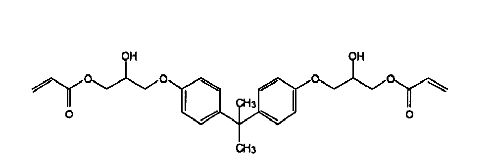


- Polmymerizable compounds in the polymerizable composition of the present invention preferably comprises 50 to 100% by weight of the (meth)acrylate having a polycyclic aromatic skeleton consisting of SP2 carbon atoms and 0 to 50% by weight of the other (meth)acrylate, more preferably 70 to 100% by weight of the (meth)acrylate having a polycyclic aromatic skeleton consisting of SP2 carbon atoms and 0 to 30% by weight of the other (meth)acrylate.
- The polymerizable composition may contain a polymerizable monomer other than (meth)acrylates without diverting the gist of the present invention.
- The polymerizable composition used in the present invention may comprise an acidic monomer. The inclusion of the acidic monomer enhances adhesiveness between layers. The acidic monomer used in the present invention is preferably monomers having a carbonic acid group or a phosphate group, more preferably (meth)acrylates having a carbonic acid group or a phosphate group, still more preferably (meth)acrylates having a phosphate group.
- The (meth) acrylate having a phosphate group is preferably a compound represented by the formula (P). The inclusion of the (meth)acrylate compound having a phosphorester group ehnances adhesion to the inorganic layer.
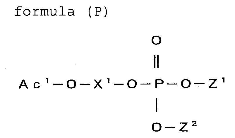
- The compound represented by the formula (P) is preferably a monofunctional monomer represented by the formula (P-1), a bifunctional monomer represented by the formula (P-2), or a trifunctional monomer represented by the formula (P-3):


- The definitions of Ac1, Ac2, Ac3, X1, X2 and X3 are the same as those in the formula (P). In the formula (P-1) and formula (P-2), R1 represents a substituent not having a polymerizable group or a hydrogen atom, and R2 represents a substituent group not having a polymerizable group, or a hydrogen atom.
- In the formula (P), (P-1), (P-2) and (P-3), X1, X2 and X3 each are the same groups as those of L1 in the formula (2), preferably an alkylene group or an alkyleneoxycarbonylalkylene group.
- In the formula (P), (P-1), (P-2) and (P-3), examples of the substituent not having a polymerizable group include an alkyl group, an aryl group, and a group consisting of a combination thereof, preferably an alkyl group.
- The carbon number of the alkyl group is preferably 1 to 12, more preferably 1 to 9, still more preferably 1 to 6. Examples of the alkyl group include a methyl group, an ethyl group, a propyl group, a butyl group, a pentyl group and a hexyl group. The alkyl group may be a linear, branched, or cyclic group, preferably a linear alkyl group. The alkyl group may be substituted with an alkoxy group, an aryl group, an aryloxy group, or the like.
- The carbon number of the aryl group is preferably 6 to 14, more preferably 6 to 10. Examples of the aryl group include a phenyl group, a 1-naphthyl group and a 2-naphtyl group. The aryl group may be substituted with an alkyl group, an alkoxy group, an aryloxy group, or the like.
- In the present invention, the monomer represented by the formula (P) may be used singly or as combined. When the compounds are used as combined, may be used a combination comprising two or more kinds of a monofunctional compound represented by the formula (P-1), a bifunctional compound represented by the formula (P-2) and a trifunctional compound represented by the formula (P-3).
- In the present invention, as the above polymerizable monomers having a phosphate group, may be used commercially available compounds such as KAYAMER series manufactured by NIPPON KAYAKU CO., LTD, and Phosmer series manufactured by Uni chemical, and a compound newly synthesized.
- Specific examples of the (meth)acrylate having a phosphate group, which is preferably used in the present invention, mentioned below, to which, however, the present invention should not be limited.


- The polymerizable composition in the present invention may include a polymerization initiator. In the case where a photopolymerization initiator is used, its amount is preferably at least 0.1 mol% of the total amount of the polymerizing compound, more preferably from 0.5 to 2 mol%. By setting the thus-designed composition, polymerization reaction though an active ingredient forming reaction may be suitably controlled. Examples of the photopolymerization initiator include Ciba Speciality Chemicals' commercial products, Irgacure series (e.g., Irgacure 651, Irgacure 754, Irgacure 184, Irgacure 2959, Irgacure 907, Irgacure 369, Irgacure 379, Irgacure 819), Darocure series (e.g., Darocure TPO, Darocure 1173), Quantacure PDO; Lamberti's commercial products, Ezacure series (e.g., Ezacure TZM, Ezacure TZT, Ezacure KT046), etc.
- The method for forming the organic layer is not specifically defined. For example, the layer may be formed according to a solution coating method or a vacuum film formation method. The solution coating method is, for example, a dipping method, an air knife coating method, a curtain coating method, a roller coating method, a wire bar coating method, a gravure coating method, a slide coating method, or an extrusion coating method using a hopper as in
USP 2681294 . The vacuum film formation method is not specifically defined, but is preferably a film formation method by vapor deposition or plasma CVD. In the present invention, the polymer may be applied for coating as its solution, or a hybrid coating method along with an inorganic material, as inJP-A 2000-323273 2004-25732 - In the present invention, the composition comprising the polymerizable monomer is cured by irradiation. The light for irradiation is generally a UV ray from a high-pressure mercury lamp or low-pressure mercury lamp. The radiation energy is preferably at least 0.1 J/cm2, more preferably at least 0.5 J/cm2. (Meth)acrylate series compounds may suffer from interference in polymerization owing to oxygen in air, and therefore, in their polymerization, the oxygen concentration or the oxygen partial pressure is preferably lowered. In the case where the oxygen concentration in polymerization is lowered according to a nitrogen purging method, the oxygen concentration is preferably not more than 2%, more preferably not more than 0.5%. In the case where the oxygen partial pressure in polymerization is lowered by a pressure reduction method, the whole pressure is preferably not more than 1000 Pa, more preferably not more than 100 Pa. Especially preferred is UV polymerization with at least 0.5 J/cm2 energy radiation under a condition of reduced pressure of not more than 100 Pa.
- The organic layer in the present invention is preferably smooth and preferably has high film hardness. Preferably, the rate of polymerization of monomer is mot less than 85%, more preferably not less than 88%, even more preferably not less than 90%, still more preferably not less than 92%. The rate of polymerization as referred to herein means the ratio of the reacted polymerizable group to all the polymerizing group (acryloyl group and methacryloyl group) in the monomer mixture. The rate of polymerization may be quantitatively determined according to IR absorptiometry.
- The thickness of the organic layer is not specifically defined. However, when the layer is too thin, then its thickness could hardly keep uniformity; but when too thick, the layer may be cracked by external force applied thereto and its barrier property may lower. From these viewpoints, the thickness of the organic layer is preferably from 50 nm to 2000 nm, more preferably from 200 nm to 1500 nm.
- As so mentioned in the above, the organic layer is preferably smooth. The mean roughness (Ra) at 1 µm square is preferably not more than 1 nm, more preferably not more than 0.5 nm. The surface of the organic layer is required not to have impurities and projections such as particles. Accordingly, it is desirable that the organic layer is formed in a clean room. The degree of cleanness is preferably not more than class 10000, more preferably not more than class 1000.
- Preferably, the hardness of the organic layer is higher. It is known that, when the hardness of the organic layer is high, then the inorganic layer may be formed smoothly and, as a result, the barrier level of the gas barrier film is thereby improved. The hardness of the organic layer may be expressed as a microhardness based on a nano-indentation method. The microhardness of the organic layer is preferably at least 100 N/mm, more preferably at least 150 N/mm.
- The inorganic layer is, in general, a layer of a thin film formed of a metal compound. For forming the inorganic layer, employable is any method capable of producing the intended thin film. For it, for example, suitable are physical vapor deposition methods (PVD) such as vapor evaporation method, sputtering method, ion plating method; various chemical vapor deposition methods (CVD); liquid phase growth methods such as plating or sol-gel method. Not specifically defined, the component to be in the inorganic layer may be any one satisfies the above-mentioned requirements. For example, it includes metal oxides, metal nitrides, metal carbides, metal oxide-nitrides, or metal oxide-carbides. Preferably used are oxides, nitrides, carbides, oxide-nitrides, or oxide-carbides comprising at least one metal selected from Si, Al, In, Sn, Zn, Ti, Cu, Ce and Ta. Of those, preferred are oxides, nitrides, or oxide-nitrides of a metal selected from Si, Al, In, Sn, Zn and Ti; more preferred are oxides, nitrides or oxide-nitrides with Si or Al. These may contain any other element as a subsidiary component.
- Preferably, the surface smoothness of the inorganic layer formed in the present invention is less than 1 nm in terms of the mean roughness (Ra value) at 1 µm square, more preferably not more than 0.5 nm.
- Not specifically defined, the thickness of the inorganic layer is generally within a range of from 5 to 500 nm/layer, preferably from 10 to 200 nm/layer. The inorganic layer may be a laminate composed of a plurality of sub-layers. In this case, each sub-layer may have the same composition, or a different composition. In addition, as so mentioned hereinabove and as disclosed in UP Laid-Open 2004-46497, the inorganic layers may be gradation layers of which the composition changes continuously in the thickness direction of the layer, with no definite boundary to the adjacent inorganic layer.
- The organic layer and the inorganic layer may be laminated by repeated film formation to form the organic layer and the inorganic layer in a desired layer constitution. In case where the inorganic layer is formed according to a vacuum film formation method such as sputtering method, vacuum evaporation method, ion plating method or plasma CVD method, then it is desirable that the organic layer is also formed according to a vacuum film formation method such as the above-mentioned flash vapor deposition method. While the barrier layer is formed, it is especially desirable that the organic layer and the inorganic layer are laminated all the time in a vacuum of not more than 1000 Pa, not restoring the pressure to an atmospheric pressure during the film formation. More preferably, the pressure is not more than 100 Pa, even more preferably not more than 50 Pa, still more preferably not more than 20 Pa.
- Particularly, in the case where at least two organic layers and at least two inorganic layers are laminated alternately, the present invention can achieve higher barrier property. The alternate layer constitution may be a layer constitution in which an organic layer, an inorganic layer, an organic layer and an inorganic layer are laminated in that order from its substrate site, or a layer constitution in which an inorganic layer, an organic layer, an inorganic layer and an organic layer are laminated in that order from its substrate site.
- The device of the present invention may have a functional layer on the barrier laminate or in any other position. The functional layer is described in detail in
JP-A 2006-289627 - In general, the barrier laminate of the present invention is formed on a support. Selecting the support, the barrier laminate may have various applications. The support includes a substrate film, as well as various devices, optical members, etc. Concretely, the barrier laminate of the present invention may be used as a barrier layer of a gas barrier film. The barrier laminate and the gas barrier film of the present invention may be used for sealing up devices that require gas-barrier property. The barrier laminate and the gas barrier film of the present invention may apply optical members. These are described in detail hereinunder.
- The gas barrier film comprises a substrate film and a barrier laminate formed on the substrate film. In the gas barrier film, the barrier laminate of the present invention may be provided only one surface of the substrate film, or may be provided on both surfaces thereof. The barrier laminate of the present invention may be laminated in an order of an inorganic layer and an organic layer from the side of the substrate film; or may be laminated in an order of an organic layer and an inorganic layer from it. The uppermost layer of the laminate of the present invention may be an inorganic layer or an organic layer.
- The gas barrier film of the present invention is a film substrate having a barrier layer that functions to block oxygen, water, nitrogen oxide, sulfur oxide, ozone and others in air.
- Not specifically defined, the number of the layers that constitute the gas barrier film may be typically from 2 layers to 30 layers, more preferably from 3 layers to 20 layers.
- The gas barrier film may have any other constitutive components (e.g., functional layers such as adhesive layer) in addition to the barrier laminate and the substrate film. The functional layer may be disposed on the barrier laminate, or between the barrier laminate and the substrate film, or on the side (back) of the substrate film not coated with the barrier laminate.
- In the gas barrier film of the present invention, the substrate film is generally a plastic film. Not specifically defined in point of the material and the thickness thereof, the plastic film usable herein may be any one capable of supporting a laminate of an organic layer and an inorganic layer; and it may be suitably selected depending on the use and the object thereof. Concretely, the plastic film includes thermoplastic resins such as polyester resin, methacryl resin, methacrylic acid-maleic anhydride copolymer, polystyrene resin, transparent fluororesin, polyimide, fluoropolyimide resin, polyamide resin, polyamidimide resin, polyetherimide resin, cellulose acylate resin, polyurethane resin, polyether ether ketone resin, polycarbonate resin, alicyclic polyolefin resin, polyarylate resin, polyether sulfone resin, polysulfone resin, cycloolefin copolymer, fluorene ring-modified polycarbonate resin, alicyclic-modified polycarbonate resin, fluorene ring-modified polyester resin, acryloyl compound.
- In case where the gas barrier film of the present invention is used as a substrate of a device such as an organic EL device to be mentioned hereinunder, it is desirable that the plastic film is formed of a heat-resistant material. Concretely, the plastic film is preferably formed of a heat-resistant transparent material having a glass transition temperature (Tg) of not lower than 100°C and/or a linear thermal expansion coefficient of not less than 40 ppm/°C. Tg and the linear expansion coefficient may be controlled by the additives to the material. The thermoplastic resin of the type includes, for example, polyethylene naphthalate (PEN: 120°C), polycarbonate (PC: 140°C), alicyclic polyolefin (e.g., Nippon Zeon's Zeonoa 1600: 160°C), polyarylate (PAr: 210°C), polyether sulfone (PES: 220°C), polysulfone (PSF: 190°C), cycloolefin copolymer (COC, compound described in
JP-A 2001-150584 JP-A 2000-227603 JP-A 2000-227603 JP-A 2002-80616 - In the case where the gas barrier film of the present invention is used in combination with a polarizing plate, it is preferable that the gas barrier layer surface of the gas barrier film is faced at the inside of a cell and is disposed in the innermost (adjacent to the device). At that time, since the gas barrier film is disposed in the inside of the cell relative to the polarizing plate, a retardation value of the gas barrier film is important. As to a use form of the gas barrier film in such an embodiment, it is preferable that a barrier film using a base material film having a retardation value of not more than 10 nm and a circular polarizing plate ((quarter-wave plate) + (half-wave plate) + (linear polarizing plate)) are laminated and used, or that a linear polarizing plate is combined with a gas barrier film using a base material film having a retardation value of from 100 nm to 180 nm, which can be used as a quarter-wave plate, and used.
- Examples of the base material film having a retardation of not more than 10 nm include cellulose triacetate (FUJITAC, manufactured by Fujifilm Corporation), polycarbonates (PURE-ACE, manufactured by Teijin Chemicals Ltd.; and ELMECH, manufactured by Kaneka Corporation), cycloolefin polymers (ARTON, manufactured by JSR Corporation; and ZEONOR, manufactured by Zeon Corporation), cycloolefin copolymers (APEL (pellet), manufactured by Mitsui Chemicals, Inc.; and TOPAS (pellet), manufactured by Polyplastics Co., Ltd.), polyarylates (U100 (pellet), manufactured by Unitika Ltd.) and transparent polyimides (NEOPULIM, manufactured by Mitsubishi Gas Chemical Company).
- Also, films obtained by properly stretching the foregoing film to adjust it so as to have a desired retardation value can be used as the quarter-wave plate.
- In view of the matter that the gas barrier film of the present invention is utilized as a device such as organic EL devices, the plastic film must be transparent, namely its light transmittance is usually not less than 80%, preferably not less than 85%, and more preferably not less than 90%. The light transmittance can be measured by a method described in JIS-K7105, namely by measuring a total light transmittance and an amount of scattered light using an integrating sphere type light transmittance analyzer and subtracting the diffuse transmittance from the total light transmittance.
- Even in the case where the gas barrier film of the present invention is used for display use, for example, when it is not disposed on the side of an observer, the transparency is not always required. Accordingly, in such case, an opaque material can also be used as the plastic film. Examples of the opaque material include a known liquid crystal polymer such as polyimides and polyacrylonitrile.
- The thickness of the plastic film to be used for the gas barrier film of the present invention is properly chosen depending upon the use and therefore, is not particularly limited. It is typically from 1 to 800 µm, preferably from 10 to 200 µm. These plastic films may have a functional layer such as a transparent conductive layer and a primer layer. The functional layer is described in detail in paragraphs 0036 to 0038 of
JP-A-2006-289627 - The barrier laminate and the gas barrier film of the present invention are favorably used for devices that are deteriorated by the chemical components in air (e.g., oxygen, water, nitrogen oxide, sulfur oxide, ozone). Examples of the devices are, for example, organic EL devices, liquid-crystal display devices, thin-film transistors, touch panels, electronic papers, solar cells, other electronic devices. More preferred are organic EL devices.
- The barrier laminate of the present invention may be used for film-sealing of devices. Specifically, this is a method of providing a barrier laminate of the present invention on the surface of a device serving as a support by itself. Before providing the barrier laminate, the device may be covered with a protective layer.
- The gas barrier film of the present invention may be used as a substrate of a device or as a film for sealing up according to a solid sealing method. The solid sealing method comprises forming a protective layer on a device, then forming an adhesive layer and a gas barrier film as laminated thereon, and curing it. Not specifically defined, the adhesive may be a thermosetting epoxy resin, a photocurable acrylate resin, etc.
- Examples of an organic EL device with a gas barrier film are described in detail in
JP-A 2007-30387 - A reflection-type liquid-crystal display device has a constitution of a lower substrate, a reflection electrode, a lower alignment film, a liquid-crystal layer, an upper alignment film, a transparent electrode, an upper substrate, a λ/4 plate and a polarizing film, formed in that order from the bottom. In this, the gas barrier film of the present invention may be used as the transparent electrode substrate and the upper substrate. In color displays, it is desirable that a color filter layer is additionally provided between the reflection electrode and the lower alignment film, or between the upper alignment film and the transparent electrode. A transmission-type liquid-crystal display device has a constitution of a backlight, a polarizer, a λ/4 plate, a lower transparent electrode, a lower alignment film, a liquid-crystal layer, an upper alignment film, an upper transparent electrode, an upper substrate, a λ/4 plate and a polarizing film, formed in that order from the bottom. In this, the substrate of the present invention may be sued as the upper transparent electrode and the upper substrate. In color displays, it is desirable that a color filter layer is additionally provided between the lower transparent electrode and the lower alignment film, or between the upper alignment film and the transparent electrode. Not specifically defined, the type of the liquid-crystal cell is preferably a TN (twisted nematic) type, an STN (super-twisted nematic) type, a HAN (hybrid aligned nematic) type, a VA (vertically alignment) type, an ECB (electrically controlled birefringence) type, anOCB (optically compensatory bent) type, an IPS (in-plane switching) type, or a CPA (continuous pinwheel alignment) type.
- The gas barrier film of the invention can be used also as a sealing film for solar cell devices. Preferably, the gas barrier film of the invention is used for sealing a solar cell device in such a manner that its adhesive layer is on the side near to the solar cell device. The solar cell devices for which the gas barrier film of the invention is favorably used are not specifically defined. For example, they include single crystal silicon-based solar cell devices, polycrystalline silicon-based solar cell devices, single-junction or tandem-structure amorphous silicon-based solar cell devices, gallium-arsenic (GaAs), indium-phosphorus (InP) or the like III-V Group compound semiconductor-based solar cell devices, cadmium-tellurium (CdTe) or the like II-VI Group compound semiconductor-based solar cell devices, copper/indium/selenium (CIS-based), copper/indium/gallium/selenium (CIGS-based), copper/indium/gallium/selenium/sulfur (CIGSS-based) or the like I-III-VI Group compound semiconductor-based solar cell devices, dye-sensitized solar cell devices, organic solar cell devices, etc. Above all, in the invention, the solar cell devices are preferably copper/indium/selenium (CIS-based), copper/indium/gallium/selenium (CIGS-based), copper/indium/gallium/selenium/sulfur (CIGSS-based) or the like I-III-VI Group compound semiconductor-based solar cell devices.
- The gas barrier film of the invention can be used in an electronic paper. The electronic paper is a reflection-type electronic display capable of attaining a high precision and a high contrast.
- The electronic paper has a display media and a TFT driving the display media on a substrate. Any known display media can be used in the electronic paper. For example, any display media of electophoretic-type, electopowder flight-type, charged tonner-type, electrochromic type can be preferably used. Among them, electophoretic display media is more preferable and microcapsule-type electophoretic display media is particularly preferable. The electophoretic display media has a plural number of capsules and each capsule has at least one particle capable of moving in a suspension flow. The at least one particle is preferably an electrophoretic particle or a spinning ball. The electrophretic display media has a first plane and a second plane that are placed in parallel, and an image is displayed through one of the two planes.
- A TFT formed on a substrate comprises a gate electrode, gate insulating layer, an active layer, a source electrode and a drain electrode. A TFT also comprises a resistance layer between the active layer and the source electrode and/or between the active layer and the drain electrode to attain electric connection.
- When a color display with a high precision is produced, TFT's are preferably formed on a color filter to precisely align them. Normal TFT with a low electric efficiency can not be down-sized much while obtaining the necessary driving current, and when a high precision display is pursued, the rate of the area for the TFT in a pixel must be high. When the rate of the area for the TFT is high, the rate of the opening area and contrast are low.
Even when a transparent amorphous IGZO-type TFT is used, light transmittance is not 100% and reduction of contrast is unavoidable. Use of the TFT disclosed inJP-A 2009-21554 - Other applications of the invention are thin-film transistors as in
JP-T H10-512104 JP-A 5-127822 2002-48913 - An example of the optical member that comprises the barrier laminate of the present invention is a circular polarizer.
- Laminating a gas barrier film of the invention with a λ/4 plate and a polarizer gives a circular polarizer. In this case, the components are so laminated that the slow axis of the λ/4 plate could cross the absorption axis of the polarizer at an angle of 45°. The polarizer is preferably stretched in the direction of 45° from the machine direction (MD) thereof; and for example, those described in
JP-A 2002-865554 - The characteristics of the present invention are described more concretely with reference to the following Examples. Accordingly, the present invention should not be limitatively interpreted by the Examples mentioned below. Formation of Gas Barrier Film (1)
- A polyethylene naphthalate film (PEN film, having a thickness of 100 µm, Teijin DuPont's trade name, Teonex Q65FA) was cut into 20 cm square pieces, and a barrier laminate was formed on the side of the smooth surface thereof, and the thus-constructed samples were evaluated.
- On the PEN film, a mixture solution of a monomer mixture having a composition shown in the following table (20 g), a UV polymerization initiator (Ciba, Irgacure 907) (0.6 g) and 2-butanone (190 g) was applied, using a wire bar. This was put into a chamber having an oxygen concentration of 0.1% after nitrogen substitution, and the organic layer was cured therein through irradiation with UV light from a high-pressure mercury lamp (integrated radiation, about 1 J/cm2), thereby forming an organic layer having a thickness of 1000 nm ± 50 nm.
- Using a sputtering device, an inorganic layer (aluminium oxide) was formed on the above organic layer. Aluminium was used as the target; argon was used as the discharge gas; and oxygen was used as the reaction gas. The film formation pressure was 0.1 Pa; and the ultimate film thickness was 50 nm. In that manner, gas barrier films having an inorganic layer laminated on an organic layer were constructed.
- The characteristic values (Ra, water vapor permeability) of the obtained gas barrier films are shown in Table 1. (Determination of Water Vapor Permeability according to Ca Method (Barrier property))
- According to the method described by G. NISATO, P. C. P. BOUTEN, P. J. SLIKKERVEER, et all, in SID Conference Record of the International Display Research Conference, pp. 1435-1438 (measurement method with calcium), the samples were analyzed for the water vapor permeability at 40°C and a relative humidity of 90%.
×: not less than 0.005 g/m2/day
○ : not less than 0.001 g/m2/day to less than 0.005 g/m2/day
○○ : less than 0.001 g/m2/day - Using an atomic force microscope (AFM), the surface smoothness of the inorganic layer formed in the above (2) was measured. In this case, the smoothness was expressed as a mean roughness Ra within a sample area of 1 µm square. The Ra was evaluated by the following gauge.
××: not less than 3 nm
×: not less than 1 nm to less than 3 nm
○ : less than 1 nm


- As is clear from the result of the above table, all the gas barrier films of the present invention showed the Water Vapor Permeability of less than 0.005 g/m2/day. The inorganic layer in the present invention achieved its surface smoothness. It was found that particularly excellent effect was achieved by using Compound C, which has two functional groups, as the (meth)acrylate having a polycyclic aromatic structure, and Compound E, which is a (meth) acrylate having three or more functional groups.
- A gas barrier film having a multilayer structure was formed in the same manner as the gas barrier film formed in the above 1, in which, however, further two organic layers and two inorganic layers were laminated thereon. It was confirmed that each gas barrier film has higher barrier property than each gas barrier film corresponding to the gas barrier film formed in the above 1.
- Gas barrier films of Examples 5 to 8 were formed in the same manner as in the above, expect that the compositions of the first layer (organic layer) were changed to compositions comprising a polymerizable monomer shown in Table 1 (19 g), a phosphoester acrylate shown below (manufactured by NIPPON KAYAKU Co., Ltd., KAYAMER PM-21, 1 g), a UV polymerization initiator (manufactured by Lamberti, Ezacure KT046, 0. 6 g) and 2-butanone (190 g). The water vapor permeability (barrier property) of the obtained gas barrier films were evaluated by the same method, then obtaining similar properties. Also, adhesiveness for the gas barrier films was evaluated by the following method.

- In order to evaluate adhesiveness of each gas barrier films, cross-cut adhesiveness test compliant to JIS K5400 was carried out. The surface of the gas barrier films having the above construction was cut in at the entering angle of 90 degree toward the film surface at 1 mm interval, thereby producing one hundred of cross-cut at 1 mm interval. On the surface thereof, Mylar tape having the wide of 2 cm (manufactured by Nitto Denko, polyester tape, No. 31B) was attached, and then was peeled off using a tape peeling testing machine. The results are shown according to the following gauge.
⊚ : 90 or more of cross-cut of 100 of cross-cut remain without peeling
○ : 50 or more of cross-cut of 100 of cross-cut remain without peeling
X: less than 50 of cross-cut of 100 of cross-cut remain[Table 2] Monomer 1 Monomer 2 Barrier property Adhesiveness Species Ratio Species Ratio Example 5 A 100 - - ○ ⊚ Example 6 B 100 - - ○ ⊚ Example 7 C 100 - - ○ ⊚ Example 8 B 70 E 30 ⊚ ⊚ - An ITO film-coated conductive glass substrate (surface resistivity, 10 Ω/square) was washed with 2-propanol, and then subjected to UV-ozone treatment for 10 minutes. On this substrate (anode), the following organic compound layers were deposited in order according to a vapor deposition method.
(First Hole Transportation Layer) Copper Phthalocyanine thickness 10 nm (Second Hole Transportation Layer) N,N'-diphenyl-N,N'-dinaphthylbenzidine thickness 40 nm (Light Emission Layer serving also as electron layer) transportation Tris(8-hydroxyquinolinato)aluminium thickness 60 nm - Finally, lithium fluoride was vapor-deposited in a thickness of 1 nm and metal aluminium was in a thickness of 100 nm in that order, serving as a cathode. On this, a silicon nitride film having a thickness of 5 µm was formed according to a parallel plate CVD method, thereby constructing an organic EL device.
- Using a thermosetting adhesive (Daizo-Nichimori's Epotec 310), the device was stuck to the gas barrier film, and heated at 65°C for 3 hours to cure the adhesive. Thus sealed, 20 samples of every organic EL device were constructed.
- Immediately after their construction, the organic EL devices were driven for light emission at a voltage of 7V applied thereto, using a source measure unit, Keithley' s SMU2400 Model. Using a microscope, the surface of each sample was checked for its condition with light emission, and it was confirmed that all the devices gave uniform light emission with no dark spot.
- Next, the devices were kept in a dark room at 60°C and a relative humidity of 90% for 500 hours, and checked for the surface condition with light emission. The ratio of the samples having given darks spots larger than 300 µm in diameter are defined as a failure ratio, and the failure ratio of each device was not more than 1%.
- The barrier laminate produced by the method of the present invention has a low water vapor permeability. The present invention makes it possible to easily produce a gas barrier film having the barrier laminate of the present invention. Since the organic EL device of the present invention has a low water vapor permeability and low failure ratio, it has high industrial availability and is useful.
- In addition, since the gas barrier film of the present invention makes it possible to smooth a surface of the inorganic layer on the organic layer, it is particularly preferably in the case where it is used as a substrate of a device.
Claims (15)
- A barrier laminate comprising at least one organic layer and at least one inorganic layer, wherein the organic layer is formed by curing a polymerizable composition comprising a (meth)acrylate having a polycyclic aromatic skeleton consisting of SP2 carbon atoms.
- The barrier laminate according to Claim 1, wherein the (meth)acrylate having a polycyclic aromatic skeleton consisting of SP2 carbon atoms is represented by the following formula (1) or (2) :


- The barrier laminate according to Claim 1 or 2, wherein the (meth)acrylate having a polycyclic aromatic skeleton consisting of SP2 carbon atoms has two or more functional groups.
- The barrier laminate according to any one of Claims 1 to 3, wherein the polymerizable composition comprises a (meth)acrylate having three or more functional groups.
- The barrier laminate according to any one of Claims 1 to 4, wherein the inorganic layer comprises at least one species selected from a metal oxide, a metal nitride, a metal carbide, a metal oxide-nitride and a metal oxide-carbide.
- The barrier laminate according to any one of Claims 1 to 5, wherein the inorganic layer is formed by a sputtering method.
- The barrier laminate according to any one of Claims 1 to 6, wherein the inorganic layer comprises an oxide containing aluminium and/or silicon, or a nitride containing aluminium and/or silicon.
- The barrier laminate according to any one of Claims 1 to 7, wherein at least two organic layers and at least two inorganic layers are laminated alternately.
- A gas barrier film comprising a substrate and the barrier laminate according to any one of Claims 1 to 8 on the substrate.
- A device comprising the barrier laminate according to any one of Claims 1 to 8.
- The device according to Claim 10, having, as a substrate, the gas barrier film according to Claim 9.
- The device according to Claim 10 or 11, sealed up with the gas barrier film according to Claim 9, or the barrier laminate according to any one of Claims 1 to 8.
- The device according to any one of Claims 10 to 12, which is an electronic device.
- The device according to any one of Claims 10 to 12, which is an organic EL device.
- A method for producing the barrier laminate according to any one of Claims 1 to 8, which comprise forming the inorganic layer by a plasma process.
Applications Claiming Priority (1)
| Application Number | Priority Date | Filing Date | Title |
|---|---|---|---|
| JP2008170744 | 2008-06-30 |
Publications (2)
| Publication Number | Publication Date |
|---|---|
| EP2141190A1 true EP2141190A1 (en) | 2010-01-06 |
| EP2141190B1 EP2141190B1 (en) | 2012-03-28 |
Family
ID=41131746
Family Applications (1)
| Application Number | Title | Priority Date | Filing Date |
|---|---|---|---|
| EP20090008445 Not-in-force EP2141190B1 (en) | 2008-06-30 | 2009-06-29 | Barrier laminate, gas barrier film, device and method for producing barrier laminate |
Country Status (4)
| Country | Link |
|---|---|
| US (1) | US20090324970A1 (en) |
| EP (1) | EP2141190B1 (en) |
| JP (1) | JP5270469B2 (en) |
| AT (1) | ATE551385T1 (en) |
Cited By (1)
| Publication number | Priority date | Publication date | Assignee | Title |
|---|---|---|---|---|
| TWI859499B (en) * | 2021-02-08 | 2024-10-21 | 日商日東電工股份有限公司 | Polarizing plate and polarizing plate with phase difference layer |
Families Citing this family (8)
| Publication number | Priority date | Publication date | Assignee | Title |
|---|---|---|---|---|
| US8241749B2 (en) * | 2008-09-11 | 2012-08-14 | Fujifilm Corporation | Barrier laminate, gas barrier film, and device using the same |
| JP5300765B2 (en) * | 2010-03-18 | 2013-09-25 | 富士フイルム株式会社 | Gas barrier film |
| JP5823277B2 (en) * | 2011-12-12 | 2015-11-25 | 富士フイルム株式会社 | Barrier laminate, gas barrier film and device using the same |
| JP5749678B2 (en) * | 2012-03-29 | 2015-07-15 | 富士フイルム株式会社 | Gas barrier film |
| KR102120892B1 (en) * | 2013-04-25 | 2020-06-10 | 삼성디스플레이 주식회사 | Organic layer damage measuring method for thin film encapsulation and the measuring apparatus thereof |
| EP3186319A4 (en) | 2014-07-25 | 2018-04-18 | Kateeva, Inc. | Organic thin film ink compositions and methods |
| CN107922766A (en) | 2015-08-31 | 2018-04-17 | 科迪华公司 | Organic film ink composite based on two and single (methyl) acrylate |
| KR102890273B1 (en) * | 2017-04-21 | 2025-11-21 | 카티바, 인크. | Compositions and techniques for forming organic thin films |
Citations (22)
| Publication number | Priority date | Publication date | Assignee | Title |
|---|---|---|---|---|
| US2681294A (en) | 1951-08-23 | 1954-06-15 | Eastman Kodak Co | Method of coating strip material |
| JPH05127822A (en) | 1991-10-30 | 1993-05-25 | Daicel Chem Ind Ltd | Touch panel |
| JPH10278167A (en) | 1997-03-31 | 1998-10-20 | Toppan Printing Co Ltd | Barrier laminate and method for producing the same |
| JPH10512104A (en) | 1995-10-25 | 1998-11-17 | フィリップス エレクトロニクス ネムローゼ フェンノートシャップ | Manufacture of electronic devices with thin-film electronic circuits on organic substrates |
| JP2000227603A (en) | 1998-11-30 | 2000-08-15 | Teijin Ltd | Liquid crystal display device and transparent conductive substrate suitable therefor |
| JP2000323273A (en) | 1999-05-07 | 2000-11-24 | Dainippon Printing Co Ltd | Electroluminescence element |
| JP2001150584A (en) | 1999-11-29 | 2001-06-05 | Nippon Zeon Co Ltd | Conductive substrate and display element using the same |
| JP2002048913A (en) | 2000-08-04 | 2002-02-15 | Fuji Photo Film Co Ltd | Retardation film, circularly polarizing plate and reflective liquid crystal display device |
| JP2002080616A (en) | 2000-06-30 | 2002-03-19 | Sumitomo Bakelite Co Ltd | Polymer film for display element and substrate for display element using the same |
| JP2002086554A (en) | 2000-07-10 | 2002-03-26 | Fuji Photo Film Co Ltd | Method for stretching polymer film, method for producing polarizing film, polarizing plate and retardation film, and liquid crystal display device |
| JP2004025732A (en) | 2002-06-27 | 2004-01-29 | Fuji Photo Film Co Ltd | Gas barrier film |
| US20040046497A1 (en) | 2002-09-11 | 2004-03-11 | General Electric Company | Diffusion barrier coatings having graded compositions and devices incorporating the same |
| WO2004046497A1 (en) | 2002-11-15 | 2004-06-03 | Baker Hughes Incorporated | Releasable wireline cablehead |
| JP2004174713A (en) * | 2002-04-12 | 2004-06-24 | Sumitomo Bakelite Co Ltd | Optical film sheet and display element using the same |
| JP2004299230A (en) | 2003-03-31 | 2004-10-28 | Dainippon Printing Co Ltd | Gas barrier substrate |
| US6899963B1 (en) * | 2004-02-25 | 2005-05-31 | Eastman Kodak Company | Electroluminescent devices having pendant naphthylanthracene-based polymers |
| JP2005222777A (en) * | 2004-02-04 | 2005-08-18 | Seiko Epson Corp | ORGANIC ELECTROLUMINESCENCE ELEMENT, ITS MANUFACTURING METHOD, AND ELECTRONIC DEVICE |
| JP2006289627A (en) | 2005-04-06 | 2006-10-26 | Fuji Photo Film Co Ltd | Gas barrier film and organic device using the same |
| JP2007030387A (en) | 2005-07-28 | 2007-02-08 | Fujifilm Corp | Barrier film substrate and organic electroluminescence device using the same |
| JP2007038529A (en) * | 2005-08-03 | 2007-02-15 | Konica Minolta Holdings Inc | Gas barrier thin film laminate, gas barrier resin base material and organic electroluminescence device |
| US20070228365A1 (en) * | 2006-03-29 | 2007-10-04 | Hynix Semiconductor Inc | Organic anti-reflective coating polymer, organic anti-reflective coating composition comprising the coating polymer and method for forming photoresist pattern using the coating composition |
| JP2009021554A (en) | 2007-06-11 | 2009-01-29 | Fujifilm Corp | Electronic display |
Family Cites Families (11)
| Publication number | Priority date | Publication date | Assignee | Title |
|---|---|---|---|---|
| US5026135A (en) * | 1990-04-20 | 1991-06-25 | E. I. Du Pont De Nemours And Company | Moisture sealing of optical waveguide devices with doped silicon dioxide |
| JP2692035B2 (en) * | 1994-05-13 | 1997-12-17 | 富士写真フイルム株式会社 | Thin film manufacturing method |
| US5635105A (en) * | 1994-05-13 | 1997-06-03 | Fuji Photo Film Co., Ltd. | Liquid crystal display and optical compensatory sheet and process for preparation of the same |
| TW445380B (en) * | 1996-10-23 | 2001-07-11 | Sumitomo Chemical Co | Plasma display front panel |
| JP4254350B2 (en) * | 2002-12-16 | 2009-04-15 | 住友ベークライト株式会社 | Transparent barrier film |
| US7101923B2 (en) * | 2003-10-03 | 2006-09-05 | General Electric Company | Flame-retardant thermoset composition, method, and article |
| JP4644868B2 (en) * | 2005-08-19 | 2011-03-09 | 株式会社メガチップス | Road sign display system |
| DE602007000572D1 (en) * | 2006-03-29 | 2009-04-09 | Fujifilm Corp | Laminated film with gas barrier properties |
| US20080221291A1 (en) * | 2007-03-07 | 2008-09-11 | 3M Innovative Properties Company | Microstructured optical films comprising biphenyl difunctional monomers |
| US8187718B2 (en) * | 2008-04-14 | 2012-05-29 | Fujifilm Corporation | Barrier laminate, barrier film substrate and device |
| US8350451B2 (en) * | 2008-06-05 | 2013-01-08 | 3M Innovative Properties Company | Ultrathin transparent EMI shielding film comprising a polymer basecoat and crosslinked polymer transparent dielectric layer |
-
2009
- 2009-06-23 JP JP2009149090A patent/JP5270469B2/en not_active Expired - Fee Related
- 2009-06-29 EP EP20090008445 patent/EP2141190B1/en not_active Not-in-force
- 2009-06-29 US US12/493,596 patent/US20090324970A1/en not_active Abandoned
- 2009-06-29 AT AT09008445T patent/ATE551385T1/en active
Patent Citations (22)
| Publication number | Priority date | Publication date | Assignee | Title |
|---|---|---|---|---|
| US2681294A (en) | 1951-08-23 | 1954-06-15 | Eastman Kodak Co | Method of coating strip material |
| JPH05127822A (en) | 1991-10-30 | 1993-05-25 | Daicel Chem Ind Ltd | Touch panel |
| JPH10512104A (en) | 1995-10-25 | 1998-11-17 | フィリップス エレクトロニクス ネムローゼ フェンノートシャップ | Manufacture of electronic devices with thin-film electronic circuits on organic substrates |
| JPH10278167A (en) | 1997-03-31 | 1998-10-20 | Toppan Printing Co Ltd | Barrier laminate and method for producing the same |
| JP2000227603A (en) | 1998-11-30 | 2000-08-15 | Teijin Ltd | Liquid crystal display device and transparent conductive substrate suitable therefor |
| JP2000323273A (en) | 1999-05-07 | 2000-11-24 | Dainippon Printing Co Ltd | Electroluminescence element |
| JP2001150584A (en) | 1999-11-29 | 2001-06-05 | Nippon Zeon Co Ltd | Conductive substrate and display element using the same |
| JP2002080616A (en) | 2000-06-30 | 2002-03-19 | Sumitomo Bakelite Co Ltd | Polymer film for display element and substrate for display element using the same |
| JP2002086554A (en) | 2000-07-10 | 2002-03-26 | Fuji Photo Film Co Ltd | Method for stretching polymer film, method for producing polarizing film, polarizing plate and retardation film, and liquid crystal display device |
| JP2002048913A (en) | 2000-08-04 | 2002-02-15 | Fuji Photo Film Co Ltd | Retardation film, circularly polarizing plate and reflective liquid crystal display device |
| JP2004174713A (en) * | 2002-04-12 | 2004-06-24 | Sumitomo Bakelite Co Ltd | Optical film sheet and display element using the same |
| JP2004025732A (en) | 2002-06-27 | 2004-01-29 | Fuji Photo Film Co Ltd | Gas barrier film |
| US20040046497A1 (en) | 2002-09-11 | 2004-03-11 | General Electric Company | Diffusion barrier coatings having graded compositions and devices incorporating the same |
| WO2004046497A1 (en) | 2002-11-15 | 2004-06-03 | Baker Hughes Incorporated | Releasable wireline cablehead |
| JP2004299230A (en) | 2003-03-31 | 2004-10-28 | Dainippon Printing Co Ltd | Gas barrier substrate |
| JP2005222777A (en) * | 2004-02-04 | 2005-08-18 | Seiko Epson Corp | ORGANIC ELECTROLUMINESCENCE ELEMENT, ITS MANUFACTURING METHOD, AND ELECTRONIC DEVICE |
| US6899963B1 (en) * | 2004-02-25 | 2005-05-31 | Eastman Kodak Company | Electroluminescent devices having pendant naphthylanthracene-based polymers |
| JP2006289627A (en) | 2005-04-06 | 2006-10-26 | Fuji Photo Film Co Ltd | Gas barrier film and organic device using the same |
| JP2007030387A (en) | 2005-07-28 | 2007-02-08 | Fujifilm Corp | Barrier film substrate and organic electroluminescence device using the same |
| JP2007038529A (en) * | 2005-08-03 | 2007-02-15 | Konica Minolta Holdings Inc | Gas barrier thin film laminate, gas barrier resin base material and organic electroluminescence device |
| US20070228365A1 (en) * | 2006-03-29 | 2007-10-04 | Hynix Semiconductor Inc | Organic anti-reflective coating polymer, organic anti-reflective coating composition comprising the coating polymer and method for forming photoresist pattern using the coating composition |
| JP2009021554A (en) | 2007-06-11 | 2009-01-29 | Fujifilm Corp | Electronic display |
Non-Patent Citations (8)
| Title |
|---|
| DATABASE CAPLUS [online] CHEMICAL ABSTRACTS SERVICE, COLUMBUS, OHIO, US; 15 February 2007 (2007-02-15), ARITA, HIROAKI; FUKUDA, KAZUHIRO: "Gas-barrier ceramic film laminates, resin substrates equipped with them, and organic electroluminescent devices therewith", XP002551016, retrieved from STN Database accession no. 2007:166400 * |
| DATABASE CAPLUS [online] CHEMICAL ABSTRACTS SERVICE, COLUMBUS, OHIO, US; 19 August 2005 (2005-08-19), OBIKAWA, TAKESHI: "Organic electroluminescent devices, manufacture thereof, and electronic devices integrating the same", XP002551014, retrieved from STN Database accession no. 2005:822769 * |
| DATABASE CAPLUS [online] CHEMICAL ABSTRACTS SERVICE, COLUMBUS, OHIO, US; 24 June 2004 (2004-06-24), KUBO, HIDEKI; ITO, HISASHI; SUGISAKI, ATSUSHI; IKEDA, MASAHIRO; EGUCHI, TOSHIMASA: "Optical multilayer plastic film sheet and electroluminescent display device using the sheet", XP002551015, retrieved from STN Database accession no. 2004:507664 * |
| DATABASE WPI Week 200449, Derwent World Patents Index; AN 2004-510695, XP002551012 * |
| DATABASE WPI Week 200726, Derwent World Patents Index; AN 2007-261841, XP002551013 * |
| DATABASE WPI Week 200818, Derwent World Patents Index; AN 2008-C41297, XP002551011, OBIKAWA T: "Organic electroluminescent element for electronic device, has organic layer comprising polymer-liquid crystal layer containing organic compound having light cross-linkable mesogen and organic compound having liquid crystalline mesogen" * |
| G. NISATO; P. C. P. BOUTEN; P. J. SLIKKERVEER, SID CONFERENCE RECORD OF THE INTERNATIONAL DISPLAY RESEARCH CONFERENCE, pages 1435 - 1438 |
| KIM ET AL., JOURNAL OF VACUUM SCIENCE AND TECHNOLOGY A, vol. 23, 2005, pages 971 - 977 |
Cited By (1)
| Publication number | Priority date | Publication date | Assignee | Title |
|---|---|---|---|---|
| TWI859499B (en) * | 2021-02-08 | 2024-10-21 | 日商日東電工股份有限公司 | Polarizing plate and polarizing plate with phase difference layer |
Also Published As
| Publication number | Publication date |
|---|---|
| US20090324970A1 (en) | 2009-12-31 |
| JP5270469B2 (en) | 2013-08-21 |
| ATE551385T1 (en) | 2012-04-15 |
| EP2141190B1 (en) | 2012-03-28 |
| JP2010030292A (en) | 2010-02-12 |
Similar Documents
| Publication | Publication Date | Title |
|---|---|---|
| EP2138533B1 (en) | Barrier laminate, gas barrier film and device using the same | |
| EP2301748B1 (en) | Barrier laminate and gas barrier film using the same | |
| US8329306B2 (en) | Barrier laminate, gas barrier film, and device using the same | |
| EP2128191B1 (en) | Barrier laminate, gas barrier film, device, and method for producing barrier laminate | |
| EP2110403B1 (en) | Barrier laminate, barrier film substrate and device | |
| EP2141190B1 (en) | Barrier laminate, gas barrier film, device and method for producing barrier laminate | |
| US20100003480A1 (en) | Barrier laminate, gas barrier film, device and optical member | |
| US20080305350A1 (en) | Barrier laminate, barrier film substrate, methods for producing them, and device | |
| EP2128192B1 (en) | Barrier laminate, gas barrier film and device using the same | |
| EP2138532B1 (en) | Barrier laminate, gas barrier film and device | |
| US8241749B2 (en) | Barrier laminate, gas barrier film, and device using the same | |
| JP2010234791A (en) | Barrier laminate, barrier film substrate and device | |
| EP2103645A1 (en) | Barrier laminate and method for producing same, device and optical component | |
| EP1958981B1 (en) | Barrier laminate, barrier film substrate, methods for producing them, and device | |
| JP5052418B2 (en) | Barrier laminate, gas barrier film, device and optical member |
Legal Events
| Date | Code | Title | Description |
|---|---|---|---|
| PUAI | Public reference made under article 153(3) epc to a published international application that has entered the european phase |
Free format text: ORIGINAL CODE: 0009012 |
|
| AK | Designated contracting states |
Kind code of ref document: A1 Designated state(s): AT BE BG CH CY CZ DE DK EE ES FI FR GB GR HR HU IE IS IT LI LT LU LV MC MK MT NL NO PL PT RO SE SI SK TR |
|
| 17P | Request for examination filed |
Effective date: 20100505 |
|
| 17Q | First examination report despatched |
Effective date: 20100625 |
|
| GRAP | Despatch of communication of intention to grant a patent |
Free format text: ORIGINAL CODE: EPIDOSNIGR1 |
|
| GRAS | Grant fee paid |
Free format text: ORIGINAL CODE: EPIDOSNIGR3 |
|
| GRAA | (expected) grant |
Free format text: ORIGINAL CODE: 0009210 |
|
| AK | Designated contracting states |
Kind code of ref document: B1 Designated state(s): AT BE BG CH CY CZ DE DK EE ES FI FR GB GR HR HU IE IS IT LI LT LU LV MC MK MT NL NO PL PT RO SE SI SK TR |
|
| REG | Reference to a national code |
Ref country code: GB Ref legal event code: FG4D |
|
| REG | Reference to a national code |
Ref country code: CH Ref legal event code: EP |
|
| REG | Reference to a national code |
Ref country code: AT Ref legal event code: REF Ref document number: 551385 Country of ref document: AT Kind code of ref document: T Effective date: 20120415 |
|
| REG | Reference to a national code |
Ref country code: IE Ref legal event code: FG4D |
|
| REG | Reference to a national code |
Ref country code: DE Ref legal event code: R096 Ref document number: 602009006068 Country of ref document: DE Effective date: 20120524 |
|
| REG | Reference to a national code |
Ref country code: NL Ref legal event code: VDEP Effective date: 20120328 |
|
| PG25 | Lapsed in a contracting state [announced via postgrant information from national office to epo] |
Ref country code: HR Free format text: LAPSE BECAUSE OF FAILURE TO SUBMIT A TRANSLATION OF THE DESCRIPTION OR TO PAY THE FEE WITHIN THE PRESCRIBED TIME-LIMIT Effective date: 20120328 Ref country code: LT Free format text: LAPSE BECAUSE OF FAILURE TO SUBMIT A TRANSLATION OF THE DESCRIPTION OR TO PAY THE FEE WITHIN THE PRESCRIBED TIME-LIMIT Effective date: 20120328 Ref country code: NO Free format text: LAPSE BECAUSE OF FAILURE TO SUBMIT A TRANSLATION OF THE DESCRIPTION OR TO PAY THE FEE WITHIN THE PRESCRIBED TIME-LIMIT Effective date: 20120628 |
|
| LTIE | Lt: invalidation of european patent or patent extension |
Effective date: 20120328 |
|
| PG25 | Lapsed in a contracting state [announced via postgrant information from national office to epo] |
Ref country code: LV Free format text: LAPSE BECAUSE OF FAILURE TO SUBMIT A TRANSLATION OF THE DESCRIPTION OR TO PAY THE FEE WITHIN THE PRESCRIBED TIME-LIMIT Effective date: 20120328 Ref country code: GR Free format text: LAPSE BECAUSE OF FAILURE TO SUBMIT A TRANSLATION OF THE DESCRIPTION OR TO PAY THE FEE WITHIN THE PRESCRIBED TIME-LIMIT Effective date: 20120629 Ref country code: FI Free format text: LAPSE BECAUSE OF FAILURE TO SUBMIT A TRANSLATION OF THE DESCRIPTION OR TO PAY THE FEE WITHIN THE PRESCRIBED TIME-LIMIT Effective date: 20120328 |
|
| REG | Reference to a national code |
Ref country code: AT Ref legal event code: MK05 Ref document number: 551385 Country of ref document: AT Kind code of ref document: T Effective date: 20120328 |
|
| PG25 | Lapsed in a contracting state [announced via postgrant information from national office to epo] |
Ref country code: CY Free format text: LAPSE BECAUSE OF FAILURE TO SUBMIT A TRANSLATION OF THE DESCRIPTION OR TO PAY THE FEE WITHIN THE PRESCRIBED TIME-LIMIT Effective date: 20120328 |
|
| PG25 | Lapsed in a contracting state [announced via postgrant information from national office to epo] |
Ref country code: PL Free format text: LAPSE BECAUSE OF FAILURE TO SUBMIT A TRANSLATION OF THE DESCRIPTION OR TO PAY THE FEE WITHIN THE PRESCRIBED TIME-LIMIT Effective date: 20120328 Ref country code: IS Free format text: LAPSE BECAUSE OF FAILURE TO SUBMIT A TRANSLATION OF THE DESCRIPTION OR TO PAY THE FEE WITHIN THE PRESCRIBED TIME-LIMIT Effective date: 20120728 Ref country code: RO Free format text: LAPSE BECAUSE OF FAILURE TO SUBMIT A TRANSLATION OF THE DESCRIPTION OR TO PAY THE FEE WITHIN THE PRESCRIBED TIME-LIMIT Effective date: 20120328 Ref country code: CZ Free format text: LAPSE BECAUSE OF FAILURE TO SUBMIT A TRANSLATION OF THE DESCRIPTION OR TO PAY THE FEE WITHIN THE PRESCRIBED TIME-LIMIT Effective date: 20120328 Ref country code: BE Free format text: LAPSE BECAUSE OF FAILURE TO SUBMIT A TRANSLATION OF THE DESCRIPTION OR TO PAY THE FEE WITHIN THE PRESCRIBED TIME-LIMIT Effective date: 20120328 Ref country code: SI Free format text: LAPSE BECAUSE OF FAILURE TO SUBMIT A TRANSLATION OF THE DESCRIPTION OR TO PAY THE FEE WITHIN THE PRESCRIBED TIME-LIMIT Effective date: 20120328 Ref country code: EE Free format text: LAPSE BECAUSE OF FAILURE TO SUBMIT A TRANSLATION OF THE DESCRIPTION OR TO PAY THE FEE WITHIN THE PRESCRIBED TIME-LIMIT Effective date: 20120328 Ref country code: SE Free format text: LAPSE BECAUSE OF FAILURE TO SUBMIT A TRANSLATION OF THE DESCRIPTION OR TO PAY THE FEE WITHIN THE PRESCRIBED TIME-LIMIT Effective date: 20120328 |
|
| PG25 | Lapsed in a contracting state [announced via postgrant information from national office to epo] |
Ref country code: SK Free format text: LAPSE BECAUSE OF FAILURE TO SUBMIT A TRANSLATION OF THE DESCRIPTION OR TO PAY THE FEE WITHIN THE PRESCRIBED TIME-LIMIT Effective date: 20120328 Ref country code: PT Free format text: LAPSE BECAUSE OF FAILURE TO SUBMIT A TRANSLATION OF THE DESCRIPTION OR TO PAY THE FEE WITHIN THE PRESCRIBED TIME-LIMIT Effective date: 20120730 |
|
| PG25 | Lapsed in a contracting state [announced via postgrant information from national office to epo] |
Ref country code: MC Free format text: LAPSE BECAUSE OF NON-PAYMENT OF DUE FEES Effective date: 20120630 Ref country code: NL Free format text: LAPSE BECAUSE OF FAILURE TO SUBMIT A TRANSLATION OF THE DESCRIPTION OR TO PAY THE FEE WITHIN THE PRESCRIBED TIME-LIMIT Effective date: 20120328 Ref country code: DK Free format text: LAPSE BECAUSE OF FAILURE TO SUBMIT A TRANSLATION OF THE DESCRIPTION OR TO PAY THE FEE WITHIN THE PRESCRIBED TIME-LIMIT Effective date: 20120328 Ref country code: AT Free format text: LAPSE BECAUSE OF FAILURE TO SUBMIT A TRANSLATION OF THE DESCRIPTION OR TO PAY THE FEE WITHIN THE PRESCRIBED TIME-LIMIT Effective date: 20120328 |
|
| PLBE | No opposition filed within time limit |
Free format text: ORIGINAL CODE: 0009261 |
|
| STAA | Information on the status of an ep patent application or granted ep patent |
Free format text: STATUS: NO OPPOSITION FILED WITHIN TIME LIMIT |
|
| PG25 | Lapsed in a contracting state [announced via postgrant information from national office to epo] |
Ref country code: IT Free format text: LAPSE BECAUSE OF FAILURE TO SUBMIT A TRANSLATION OF THE DESCRIPTION OR TO PAY THE FEE WITHIN THE PRESCRIBED TIME-LIMIT Effective date: 20120328 Ref country code: MK Free format text: LAPSE BECAUSE OF FAILURE TO SUBMIT A TRANSLATION OF THE DESCRIPTION OR TO PAY THE FEE WITHIN THE PRESCRIBED TIME-LIMIT Effective date: 20120328 |
|
| 26N | No opposition filed |
Effective date: 20130103 |
|
| REG | Reference to a national code |
Ref country code: IE Ref legal event code: MM4A |
|
| REG | Reference to a national code |
Ref country code: DE Ref legal event code: R097 Ref document number: 602009006068 Country of ref document: DE Effective date: 20130103 |
|
| PG25 | Lapsed in a contracting state [announced via postgrant information from national office to epo] |
Ref country code: IE Free format text: LAPSE BECAUSE OF NON-PAYMENT OF DUE FEES Effective date: 20120629 Ref country code: ES Free format text: LAPSE BECAUSE OF FAILURE TO SUBMIT A TRANSLATION OF THE DESCRIPTION OR TO PAY THE FEE WITHIN THE PRESCRIBED TIME-LIMIT Effective date: 20120709 |
|
| PG25 | Lapsed in a contracting state [announced via postgrant information from national office to epo] |
Ref country code: BG Free format text: LAPSE BECAUSE OF FAILURE TO SUBMIT A TRANSLATION OF THE DESCRIPTION OR TO PAY THE FEE WITHIN THE PRESCRIBED TIME-LIMIT Effective date: 20120628 Ref country code: MT Free format text: LAPSE BECAUSE OF FAILURE TO SUBMIT A TRANSLATION OF THE DESCRIPTION OR TO PAY THE FEE WITHIN THE PRESCRIBED TIME-LIMIT Effective date: 20120328 |
|
| REG | Reference to a national code |
Ref country code: CH Ref legal event code: PL |
|
| PG25 | Lapsed in a contracting state [announced via postgrant information from national office to epo] |
Ref country code: TR Free format text: LAPSE BECAUSE OF FAILURE TO SUBMIT A TRANSLATION OF THE DESCRIPTION OR TO PAY THE FEE WITHIN THE PRESCRIBED TIME-LIMIT Effective date: 20120328 Ref country code: CH Free format text: LAPSE BECAUSE OF NON-PAYMENT OF DUE FEES Effective date: 20130630 Ref country code: LI Free format text: LAPSE BECAUSE OF NON-PAYMENT OF DUE FEES Effective date: 20130630 |
|
| PG25 | Lapsed in a contracting state [announced via postgrant information from national office to epo] |
Ref country code: LU Free format text: LAPSE BECAUSE OF NON-PAYMENT OF DUE FEES Effective date: 20120629 |
|
| PG25 | Lapsed in a contracting state [announced via postgrant information from national office to epo] |
Ref country code: HU Free format text: LAPSE BECAUSE OF FAILURE TO SUBMIT A TRANSLATION OF THE DESCRIPTION OR TO PAY THE FEE WITHIN THE PRESCRIBED TIME-LIMIT Effective date: 20090629 |
|
| REG | Reference to a national code |
Ref country code: FR Ref legal event code: PLFP Year of fee payment: 8 |
|
| REG | Reference to a national code |
Ref country code: FR Ref legal event code: PLFP Year of fee payment: 9 |
|
| REG | Reference to a national code |
Ref country code: FR Ref legal event code: PLFP Year of fee payment: 10 |
|
| PGFP | Annual fee paid to national office [announced via postgrant information from national office to epo] |
Ref country code: DE Payment date: 20180619 Year of fee payment: 10 |
|
| PGFP | Annual fee paid to national office [announced via postgrant information from national office to epo] |
Ref country code: FR Payment date: 20180511 Year of fee payment: 10 |
|
| PGFP | Annual fee paid to national office [announced via postgrant information from national office to epo] |
Ref country code: GB Payment date: 20180627 Year of fee payment: 10 |
|
| REG | Reference to a national code |
Ref country code: DE Ref legal event code: R119 Ref document number: 602009006068 Country of ref document: DE |
|
| GBPC | Gb: european patent ceased through non-payment of renewal fee |
Effective date: 20190629 |
|
| PG25 | Lapsed in a contracting state [announced via postgrant information from national office to epo] |
Ref country code: GB Free format text: LAPSE BECAUSE OF NON-PAYMENT OF DUE FEES Effective date: 20190629 Ref country code: DE Free format text: LAPSE BECAUSE OF NON-PAYMENT OF DUE FEES Effective date: 20200101 |
|
| PG25 | Lapsed in a contracting state [announced via postgrant information from national office to epo] |
Ref country code: FR Free format text: LAPSE BECAUSE OF NON-PAYMENT OF DUE FEES Effective date: 20190630 |