EP2139306B1 - Housing for circuit board - Google Patents
Housing for circuit board Download PDFInfo
- Publication number
- EP2139306B1 EP2139306B1 EP09100346.7A EP09100346A EP2139306B1 EP 2139306 B1 EP2139306 B1 EP 2139306B1 EP 09100346 A EP09100346 A EP 09100346A EP 2139306 B1 EP2139306 B1 EP 2139306B1
- Authority
- EP
- European Patent Office
- Prior art keywords
- housing
- circuit board
- printed circuit
- wall
- projections
- Prior art date
- Legal status (The legal status is an assumption and is not a legal conclusion. Google has not performed a legal analysis and makes no representation as to the accuracy of the status listed.)
- Active
Links
Images


Classifications
-
- H—ELECTRICITY
- H05—ELECTRIC TECHNIQUES NOT OTHERWISE PROVIDED FOR
- H05K—PRINTED CIRCUITS; CASINGS OR CONSTRUCTIONAL DETAILS OF ELECTRIC APPARATUS; MANUFACTURE OF ASSEMBLAGES OF ELECTRICAL COMPONENTS
- H05K7/00—Constructional details common to different types of electric apparatus
- H05K7/14—Mounting supporting structure in casing or on frame or rack
- H05K7/1422—Printed circuit boards receptacles, e.g. stacked structures, electronic circuit modules or box like frames
- H05K7/1424—Card cages
Definitions
- the present invention relates to a housing for at least one printed circuit board.
- Housing for receiving printed circuit boards are known from the prior art, for example from DE 20215 425 U1 known, wherein the known housing is designed for at least one populated electronic circuit board and comprises spacer means which keep the circuit board at a distance from the housing bottom and also comprises fixing means for the circuit board in the housing, and wherein both the spacer means and the fixing means by a corresponding Shaping the housing are realized by the two opposite side walls of the housing bottom starting divergently upwards, in such a way that they have at a distance above the housing bottom of the respective dimension of the circuit board corresponding distance from each other and thus form the support areas for the circuit board ,
- the above known housing has, on the one hand, a spacing means which keep the printed circuit board at a distance from the housing bottom and fixing means for the printed circuit board, wherein both the spacer means and the fixing means are realized solely by a corresponding shaping of the housing.
- the above-mentioned known case further includes a cover integrally formed with mounting feet of the case.
- the spacer means of the circuit board are provided from the bottom of the housing by means of angled side walls of the housing, whereby the circuit board is indeed spaced from the ground but does not find a secure hold and thereby dictated by the geometry and dimensions of the housing.
- only identically formed printed circuit boards can be arranged in the housing.
- a housing according to the preamble of claim 1 is known from DE 10 2004 015 517 A1 known.
- a circuit board is inserted on a wall side of the housing in a groove and mounted on the opposite wall side on a heel edge.
- the US 4,791,531 discloses an extruded U-shaped housing in which printed circuit boards must be inserted in both sides provided grooves from the side.
- Object of the present invention is therefore to provide a simple and inexpensive solution for arranging at least one circuit board in a housing, which can be provided in a simple manner flexible and also variable and mounted.
- a housing for a printed circuit board comprises, in particular, an elongate integrally formed U-shaped housing base having a housing bottom and a first and a second wall and having two lateral walls which are fastened to the housing main body, wherein the housing main body according to the invention of extruded is provided, and the housing base body with the two attached to it lateral walls forms an upwardly open box-shaped housing, which is designed such that at least one circuit board from above into the housing insertable and fixable in the housing, wherein the uppermost of the circuit boards their populated side is arranged down and their other side closes the housing at the top.
- An inventive housing according to the embodiment of the present invention is particularly advantageous, since it is easy to install and can be produced in a simple manner in particular in different dimensions for different sized printed circuit boards, in particular due to the inventive design of the housing base as extruded, whose length to simple Can be varied to produce alternative device variants.
- a housing according to the invention for at least one printed circuit board comprises in particular an elongate integrally formed U-shaped housing main body with a housing bottom and a first and second wall, and with two lateral walls which are fastened to a housing base body, wherein the housing main body with the two side walls forms an upwardly open box-shaped housing which is formed such that at least one circuit board can be inserted from above into the housing and the housing is fixed, the uppermost of the printed circuit boards is arranged with its equipped side down and its other side the housing closes up and arranged on the exposed side of the circuit board sockets for connectors with cables.
- the above housing according to the invention also comprises an integral with the two side walls mounting bracket extending above the housing top off the circuit board from one side wall to the other side wall, wherein the mounting bracket is formed such that clamps or cable ties for with the sockets connected cables for strain relief of the cable to the mounting bracket are providable.
- the integral formation of the mounting bracket for clamps or cable ties for strain relief of cables with the two lateral walls of the housing is particularly advantageous since the mounting bracket can be punched with the two side walls of a metal sheet in a simple manner, and then the metal sheet can be angled to provide the side walls and the mounting bracket in a simple manner.
- the above-mentioned embodiments are also particularly advantageous because material is saved in a suitable manner, after the printed circuit board arranged above is arranged with its component side inside and below into the housing, while at the same time acts with its upwardly disposed side as a cover of the housing, which Saves material and assembly costs.
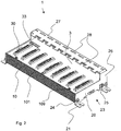
- Fig. 1 shows a schematic representation of a housing 1 for a printed circuit board 3, 3 'according to a first embodiment of the present invention in perspective view with a U - shaped housing base 10, which comprises a bottom with two opposite walls 101, 102, wherein on the housing base 10 also are attached side walls 20 which terminate the housing 1 from the side. On the side walls 20 are suitably formed feet 21, which are angled accordingly, and which allow to fix the housing 1 in a simple manner on a mounting surface.
- the cover of the housing 1 is provided by means of a non-populated base surface of a printed circuit board 3, which is arranged in the housing 1, wherein the circuit board 3 may suitably also comprise sockets 30 for the connection of cables, and also a window 33 for the view in may include the interior of the housing 1.
- the side walls comprise suitable bores 22 for corresponding fastening means.
- the upper circuit board 3 holes 34 also for suitable fastening means of the circuit board 3 to the housing base body 10th
- the housing base 10 is made of extruded profile and particularly advantageously made of extruded aluminum, so that its length can be easily changed and provided in a simple manner a variety of different variations for longer or shorter circuit boards with more or fewer connectors or outputs with sockets can be.
- Fig. 2 shows a perspective view of a housing 1 according to the invention for at least one printed circuit board 3, 3 'according to a further embodiment, which in many areas of the embodiment of Fig. 1 corresponds, which is why the same elements of the housing 1 are provided with the same reference numerals and why, for the sake of simplicity, a further description is dispensed with.
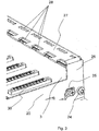
- the housing 1 of Fig. 2 further comprises a mounting bracket 27 integrally formed with the side walls 20 and extending from an upwardly projecting shoulder 26 of a side wall 20 to a corresponding second protruding shoulder 26 of the second lateral wall 20 and above and in parallel to the top of the housing 1 covering printed circuit board 3 is arranged with upwardly projecting sockets 30 for connectors of cables.
- the mounting bracket 27 includes in particular at least one suitable provided by means of recesses 28 row of holes for attachment of cable ties or cable clamps of any design for the protection of connected to the sockets 30 connectors and cables and strain relief of the cable.
- the mounting bracket 27 is integrally formed in particular with the two lateral walls 2 and suitably punched from a common metal sheet, wherein the side walls 20 are angled with their feet 21 in a suitable manner.
- Fig. 2 also shows suitable fastening means 24 for fixing the side walls to the housing base body 10 and fastening means 109 for the circuit board 3, which are respectively arranged in bores, the bores 22 and 34 of the housing 1 according to the invention of the embodiment of Fig. 1 correspond.
- a side wall 20 may also suitably include a connector 25 for grounding the housing 1.
- Fig. 3 shows an enlarged perspective view of the housing 1 of the invention Fig. 1 in a partial view with the lateral wall 20, the upwardly projecting shoulder 26 and the mounting bracket 27, in the two suitably provided by means of suitable recesses 28 row of holes are provided so that a plurality of different cable ties or clamping devices can be mounted on the mounting bracket 27.
- Fig. 4 shows a schematic representation of the housing 1 according to the invention from the rear, for the sake of simplicity, only the essential basic components of the housing 1 are provided with reference numerals, namely the housing body 10 with its one wall 102, the side wall 20 and the upper circuit board 3 and the mounting bracket 27th , wherein on the mounting bracket 27 suitably and advantageously a shutter 29 is provided which is angled down to the wall 102 out and shields the area of the clamping devices and sockets 30 to the side of the wall 102 out.
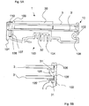
- Fig. 5A shows a schematic section through the line AA of Fig. 1 with the housing 1 with its housing base 10, which is elongated and comprises a housing bottom and two lateral walls 101, 102, and with two circuit boards 3, 3 ', which are arranged in the housing 1, wherein suitably the upper circuit board 3, the housing 1 closes up and at the same time provides a connection 30 for cable.
- one of the side walls 101, 102 on its underside a suitably formed clamping zone for easy insertion and fixation of the circuit boards 3, 3 ', each with an upper and lower appropriately formed projection 106, 105; 106 ', 105' wherein each of the lower projection 105, 105 'are angled, which allows easy mounting of the circuit boards 3, 3' in the housing 1.
- the projections 106, 105 and 106 ', 105' are also suitably arranged such that upon insertion of a circuit board 3, 3 'in the space provided between the projections 105, 106 and 105', 106 'at an angle from above and to Lowering the circuit board 3, 3 'in a horizontal position, the circuit board 3, 3' between the projections 105,106; 105 ', 106' is held securely.
- a clamping zone for the circuit boards 3, 3 ' may be formed, a clamping zone for the circuit boards 3, 3 'provided.
- the opposite wall 101 comprises a suitable paragraph for storage of the lower circuit board 3 ', which rests upon entry of the circuit board 3' in the clamping zone 105 ', 106' and after lowering the circuit board 3 'on the shoulder of the wall 101.
- the integral with the wall 101 paragraph for supporting the circuit board 3 ' suitably comprises vertical recesses 108 which correspond to the holes 34 of the circuit board 3, 3', so that suitable fasteners 109, which may be suitable and exemplary screws, the circuit board. 3 , 3 'on the housing base 10 can fix.
- a suitable spacer 110 is provided which rests on the printed circuit board 3', and on which in turn rests the upper printed circuit board 3, wherein the spacer 110 suitably also held by the fastening means 109 is and, for example, and advantageously can be sleeve-shaped.
- the housing base body 10 also advantageously comprises a contour-like bottom with a contour 103 and with cooling fins 104, for dissipating or supplying heat into or out of the housing interior, wherein suitably inside the housing 104 in the vicinity of the cooling fin 104, a suitable heat conducting element 32 may be provided has direct contact with the bottom of the housing base body 10 and the lower circuit board 3 '.
- a suitable gate 23 is formed such that the contour 103 and the cooling fins 104 are exposed laterally.
- the housing base 10 of a housing 1 also comprises suitable horizontal recesses 108 in the walls 101, 102 for receiving fastening means 24 for fastening the lateral walls 20, wherein the fastening means 24 may suitably also be screws which engage with the recesses 108 and / or in correspond to the recesses 108 formed threaded holes.
- Fig. 5B shows an enlarged view of a portion of the schematic representation of Fig. 5A with the upper and lower circuit boards 3, 3 'and the respective clamping zones 106, 105; 106 ', 105' on the inside of the wall 102, wherein advantageously in each case together with the circuit board 3, 3 'a compensation element 31 is provided on at least the bottom or the top of the circuit board 3, 3', thereby advantageously a tolerance compensation of tolerances of the strength the printed circuit board 3, 3 'is provided and also advantageously a damping of stresses and a rattle protection is provided for vibrations of the housing 1.
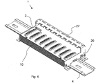
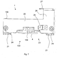
- Fig. 6 shows a perspective view of the housing 1 of the invention Fig. 2 together with a DIN rail and Fig. 7 shows a schematic side view of Fig. 6 ,
- Fig. 6 shows a perspective view of the housing 1 of the invention Fig. 2 together with a DIN rail
- Fig. 7 shows a schematic side view of Fig. 6 ,
- already described elements of the housing 1 according to the invention is dispensed with and instead to the description of the FIGS. 2 to 5 is referenced.
- an inventive housing 1 according to the embodiment according to Fig. 2 with the mounting bracket 27 advantageously corresponding clamping zones 105, 106; 105 ', 106' and the rest to the above description of Fig. 5 may include mentioned features.
- the advantageous contour 103 of the bottom of the housing base body 10 is formed such that the contour 103 corresponds to a DIN rail 4, and designed in a simple manner for receiving a DIN rail 4 is, so that the housing 1 can be inserted into an existing DIN rail 4 and can be easily attached to the feet 20 at a mounting plane.
Landscapes
- Engineering & Computer Science (AREA)
- Microelectronics & Electronic Packaging (AREA)
- Mounting Of Printed Circuit Boards And The Like (AREA)
- Casings For Electric Apparatus (AREA)
Description
Die vorliegende Erfindung bezieht sich auf ein Gehäuse für wenigstens eine Leiterplatte.The present invention relates to a housing for at least one printed circuit board.
Gehäuse zur Aufnahme von Leiterplatten sind aus dem Stand der Technik beispielsweise aus der
Das vorstehende bekannte Gehäuse weist zum einen Abstandshaltemittel auf, die die Leiterplatte gegenüber dem Gehäuseboden auf Abstand halten sowie Fixierungsmittel für die Leiterplatte, wobei sowohl die Abstandshaltemittel als auch die Fixierungsmittel allein durch eine entsprechende Formgebung des Gehäuses realisiert sind.The above known housing has, on the one hand, a spacing means which keep the printed circuit board at a distance from the housing bottom and fixing means for the printed circuit board, wherein both the spacer means and the fixing means are realized solely by a corresponding shaping of the housing.
Das vorstehend genannte bekannte Gehäuse umfasst außerdem eine Abdeckung, die einstückig mit Befestigungsfüßen des Gehäuses ausgebildet ist. Außerdem sind die Abstandshaltemittel der Leiterplatte vom Boden des Gehäuses mittels abgewinkelten seitlichen Wänden des Gehäuses bereitgestellt, wodurch die Leiterplatte zwar vom Boden beabstandet ist aber keinen sicheren Halt findet und hierbei vorgegeben durch die Geometrie und die Abmessungen des Gehäuses außerdem lediglich gleichartig ausgebildete Leiterplatten in dem Gehäuse angeordnet werden können.The above-mentioned known case further includes a cover integrally formed with mounting feet of the case. In addition, the spacer means of the circuit board are provided from the bottom of the housing by means of angled side walls of the housing, whereby the circuit board is indeed spaced from the ground but does not find a secure hold and thereby dictated by the geometry and dimensions of the housing In addition, only identically formed printed circuit boards can be arranged in the housing.
Ein Gehäuse gemäß dem Oberbegriff des Anspruchs 1 ist aus der
Die
Aufgabe der vorliegenden Erfindung ist daher eine einfache und kostengünstige Lösung zur Anordnung mindestens einer Leiterplatte in einem Gehäuse anzugeben, das auf einfache Weise flexibel und auch variabel bereitgestellt und montiert werden kann.Object of the present invention is therefore to provide a simple and inexpensive solution for arranging at least one circuit board in a housing, which can be provided in a simple manner flexible and also variable and mounted.
Die Aufgabe wird mit den Merkmalen des unabhängigen Anspruchs 1 gelöst. Vorteilhafte Ausführungen sind in den Merkmalen der Unteransprüche und/oder der nachfolgenden Beschreibung erwähnt, die von schematischen Zeichnungen begleitet ist. Hierzu zeigt:
- Fig. 1
- eine schematische perspektivische Darstellung eines erfindungsgemäßen Gehäuses für eine Leiterplatte;
- Fig. 2
- eine schematische perspektivische Darstellung eines erfindungsgemäßen Gehäuses für eine Leiterplatte nach einer weiteren Ausführung;
- Fig. 3
- einen vergrößerten Ausschnitt des Gehäuses von
Fig. 2 ; - Fig. 4
- eine perspektivische Darstellung des Gehäuses von
Fig. 2 und3 von hinten; - Fig. 5A
- einen Schnitt durch die Leiterplatte von
Fig. 1 entlang der Linie A-A vonFig. 1 undFig. 5B einen vergrößerten Ausschnitt vonFig. 5A ; - Fig. 6
- das Gehäuse von
Fig. 2 mit einer Hutschiene; die Hutschiene ist nicht Gegenstand der Erfindung; - Fig. 7
- eine Seitenansicht des Gehäuses von
Fig. 6 mit der Hutschiene.
- Fig. 1
- a schematic perspective view of a housing according to the invention for a printed circuit board;
- Fig. 2
- a schematic perspective view of a housing according to the invention for a printed circuit board according to a further embodiment;
- Fig. 3
- an enlarged section of the housing of
Fig. 2 ; - Fig. 4
- a perspective view of the housing of
Fig. 2 and3 from the back; - Fig. 5A
- a section through the circuit board of
Fig. 1 along the line AA ofFig. 1 andFig. 5B an enlarged section ofFig. 5A ; - Fig. 6
- the case of
Fig. 2 with a hat rail; the DIN rail is not the subject of the invention; - Fig. 7
- a side view of the housing of
Fig. 6 with the DIN rail.
Ein Gehäuse für eine Leiterplatte nach einer Ausführung der vorliegenden Erfindung umfasst insbesondere einen länglichen einstückig ausgebildeten U - förmigen Gehäusegrundkörper mit einem Gehäuseboden und einer ersten und einer zweiten Wand und mit zwei seitlichen Wänden, die an dem Gehäusegrundkörper befestigt sind, wobei der Gehäusegrundkörper erfindungsgemäß aus Strangpreßprofil bereitgestellt ist, und der Gehäusegrundkörper mit den beiden an ihm befestigten seitlichen Wänden ein nach oben offenes kastenförmiges Gehäuse bildet, das derart ausgebildet ist, dass wenigstens eine Leiterplatte von oben in das Gehäuse einsetzbar und in dem Gehäuse fixierbar ist, wobei die oberste der Leiterplatten mit ihrer bestückten Seite nach unten angeordnet ist und ihre andere Seite das Gehäuse oben abschließt.A housing for a printed circuit board according to an embodiment of the present invention comprises, in particular, an elongate integrally formed U-shaped housing base having a housing bottom and a first and a second wall and having two lateral walls which are fastened to the housing main body, wherein the housing main body according to the invention of extruded is provided, and the housing base body with the two attached to it lateral walls forms an upwardly open box-shaped housing, which is designed such that at least one circuit board from above into the housing insertable and fixable in the housing, wherein the uppermost of the circuit boards their populated side is arranged down and their other side closes the housing at the top.
Ein erfindungsgemäßes Gehäuse nach der Ausführung der vorliegenden Erfindung ist besonders vorteilhaft, nachdem es einfach montierbar ist und auch auf einfache Weise hergestellt werden kann insbesondere auch in verschiedenen Abmessungen für verschieden dimensionierte Leiterplatten, insbesondere aufgrund der erfindungsgemäßen Ausbildung des Gehäusegrundkörpers als Strangpreßprofil, dessen Länge auf einfache Weise variiert werden kann, um alternative Gerätevarianten zu erzeugen.An inventive housing according to the embodiment of the present invention is particularly advantageous, since it is easy to install and can be produced in a simple manner in particular in different dimensions for different sized printed circuit boards, in particular due to the inventive design of the housing base as extruded, whose length to simple Can be varied to produce alternative device variants.
Ein erfindungsgemäßes Gehäuse für wenigstens eine Leiterplatte nach einer weiteren Ausführung umfasst insbesondere einen länglichen einstückig ausgebildeten U - förmigen Gehäusegrundkörper mit einem Gehäuseboden und einer ersten und zweiten Wand, und mit zwei seitlichen Wänden, die an einem Gehäusegrundkörper befestigt sind, wobei der Gehäusegrundkörper mit den beiden seitlichen Wänden ein nach oben offenes kastenförmiges Gehäuse bildet, das derart ausgebildet ist, dass wenigstens eine Leiterplatte von oben in das Gehäuse einsetzbar und dem Gehäuse fixierbar ist, wobei die oberste der Leiterplatten mit ihrer bestückten Seite nach unten angeordnet ist und ihre andere Seite das Gehäuse nach oben abschließt und auf der nach oben freiliegenden Seite der Leiterplatte Anschlußbuchsen für Steckverbindungen mit Kabeln angeordnet sind. Das vorstehende erfindungsgemäße Gehäuse umfasst außerdem einen mit den beiden seitlichen Wänden einstückigen Befestigungsbügel, der sich oberhalb der das Gehäuse oben abschließenden Leiterplatte von einer seitlichen Wand zu der anderen seitlichen Wand erstreckt, wobei der Befestigungsbügel derart ausgebildet ist, dass Klemmbefestigungen oder Kabelbinder für mit dem Anschlußbuchsen verbundene Kabel für Zugentlastungen der Kabel an dem Befestigungsbügel vorsehbar sind.A housing according to the invention for at least one printed circuit board according to a further embodiment comprises in particular an elongate integrally formed U-shaped housing main body with a housing bottom and a first and second wall, and with two lateral walls which are fastened to a housing base body, wherein the housing main body with the two side walls forms an upwardly open box-shaped housing which is formed such that at least one circuit board can be inserted from above into the housing and the housing is fixed, the uppermost of the printed circuit boards is arranged with its equipped side down and its other side the housing closes up and arranged on the exposed side of the circuit board sockets for connectors with cables. The above housing according to the invention also comprises an integral with the two side walls mounting bracket extending above the housing top off the circuit board from one side wall to the other side wall, wherein the mounting bracket is formed such that clamps or cable ties for with the sockets connected cables for strain relief of the cable to the mounting bracket are providable.
Bei einer weiteren Ausführung ist die einstückige Ausbildung des Befestigungsbügels für Klemmvorrichtungen oder Kabelbinder für Zugentlastungen von Kabeln mit den beiden seitlichen Wänden des Gehäuses besonders vorteilhaft, da der Befestigungsbügel mit den beiden seitlichen Wänden aus einem Metallblech auf einfache Weise gestanzt werden kann, und wonach das Metallblech zur Bereitstellung der seitlichen Wände und des Befestigungsbügels auf einfache Weise abgewinkelt werden kann.In another embodiment, the integral formation of the mounting bracket for clamps or cable ties for strain relief of cables with the two lateral walls of the housing is particularly advantageous since the mounting bracket can be punched with the two side walls of a metal sheet in a simple manner, and then the metal sheet can be angled to provide the side walls and the mounting bracket in a simple manner.
Die vorstehend genannten Ausführungen sind auch besonders vorteilhaft, weil auf geeignete Weise Material gespart wird, nachdem die oben angeordnete Leiterplatte mit ihrer Bestückungsseite nach innen und unten ins Gehäuse angeordnet ist, und dabei mit ihrer nach oben angeordneten Seite zugleich als Abdeckung des Gehäuses fungiert, was Material- und Montageaufwand spart.The above-mentioned embodiments are also particularly advantageous because material is saved in a suitable manner, after the printed circuit board arranged above is arranged with its component side inside and below into the housing, while at the same time acts with its upwardly disposed side as a cover of the housing, which Saves material and assembly costs.
Die vorliegende Erfindung wird nachfolgend ohne jede Beschränkung anhand von schematischen Zeichnungen detailliert beschrieben.The present invention will now be described in detail, by way of non-limiting example, with reference to schematic drawings.
Erfindungsgemäß ist der Gehäusegrundkörper 10 aus Strangpreßprofil und insbesondere vorteilhaft aus Aluminium-Strangpreßprofil bereitgestellt, so dass seine Länge auf einfache Weise verändert werden kann und auf ebenso einfache Weise eine Vielzahl unterschiedlicher Variationen für längere oder kürzere Leiterplatten mit mehr oder weniger Steckverbindungen oder Ausgängen mit Anschlußbuchsen bereitgestellt werden kann.According to the invention, the
Das Gehäuse 1 von
Bei einer weiteren Ausführung ist der Befestigungsbügel 27 insbesondere mit den beiden seitlichen Wänden 2 einstückig ausgebildet und geeigneterweise aus einem gemeinsamen Metallblech gestanzt, wobei die seitlichen Wände 20 mit ihren Füßen 21 auf geeignete Weise abgewinkelt sind.In a further embodiment, the
Vorteilhaft umfasst eine der seitlichen Wände 101, 102 an ihrer Unterseite eine geeignet ausgebildete Klemmzone zur einfachen Einführung und festen Fixierung der Leiterplatten 3, 3' mit jeweils einem oberen und unteren geeignet ausgebildeten Vorsprung 106, 105; 106', 105' wobei jeweils der untere Vorsprung 105, 105' abgewinkelt ausgebildet sind, was eine einfache Montage der Leiterplatten 3, 3' in dem Gehäuse 1 ermöglicht. Die Vorsprünge 106, 105 bzw. 106', 105' sind außerdem geeigneterweise derart angeordnet, dass nach Einfuhr einer Leiterplatte 3, 3' in den zwischen den Vorsprüngen 105, 106 und 105', 106' bereitgestellten Raum in einem Winkel von oben und nach Absenkung der Leiterplatte 3, 3' in eine waagerechte Position die Leiterplatte 3, 3' zwischen den Vorsprüngen 105,106; 105', 106' sicher gehalten wird. Erfindungsgemäß wird dabei mit den jeweiligen Vorsprüngen 106, 105; 106', 105', die geeigneterweise schienenartig ausgebildet sein können, eine Klemmzone für die Leiterplatten 3, 3' bereitgestellt.Advantageously, one of the
Die gegenüberliegende Wand 101 umfasst einen geeigneten Absatz zur Lagerung der unteren Leiterplatte 3', die nach Einfuhr der Leiterplatte 3' in die Klemmzone 105', 106' und nach Absenkung der Leiterplatte 3' auf dem Absatz der Wand 101 aufliegt. Der mit der Wand 101 einstückig ausgebildete Absatz zur Auflage der Leiterplatte 3' umfasst geeigneterweise senkrechte Ausnehmungen 108, die mit den Bohrungen 34 der Leiterplatte 3, 3' korrespondieren, so dass geeignete Befestigungsmittel 109, die geeigneterweise und beispielhaft Schrauben sein können, die Leiterplatte 3, 3' an dem Gehäusegrundkörper 10 fixieren können. Zur Beabstandung der oberen Leiterplatte 3 von der unteren Leiterplatte 3' ist hierfür insbesondere ein geeignetes Distanzstück 110 vorgesehen, das auf der Leiterplatte 3' aufliegt, und auf dem wiederum die obere Leiterplatte 3 aufliegt, wobei das Distanzstück 110 geeigneterweise ebenfalls von dem Befestigungsmittel 109 gehalten wird und beispielsweise und vorteilhaft hülsenartig ausgebildet sein kann.The
Der Gehäusegrundkörper 10 umfasst außerdem vorteilhaft einen konturartig ausgebildeten Boden mit einer Kontur 103 und mit Kühlrippen 104, zur Ableitung oder Zufuhr von Wärme in oder aus dem Gehäuseinneren, wobei geeigneterweise im Gehäuseinneren in der Umgebung der Kühlrippe 104 ein geeignetes Wärmeleitelement 32 vorgesehen sein kann, das direkten Kontakt mit dem Boden des Gehäusegrundkörpers 10 und der unteren Leiterplatte 3' hat. Hierfür ist in den seitlichen Wänden 20 eine geeignete Kulisse 23 derart ausgebildet, dass die Kontur 103 und die Kühlrippen 104 seitlich frei liegen.The
Die vorteilhafte Kontur innerhalb der die Kühlrippen 104 des Gehäusebodens ausgebildet sind wird nachfolgend anhand von
Der Gehäusegrundkörper 10 eines erfindungsgemäßen Gehäuses 1 umfasst außerdem geeignete horizontale Ausnehmungen 108 in den Wänden 101, 102 zur Aufnahme von Befestigungsmitteln 24 zur Befestigung der seitlichen Wände 20, wobei die Befestigungsmittel 24 geeigneterweise ebenfalls Schrauben sein können, die mit den Ausnehmungen 108 und/oder in den Ausnehmungen 108 ausgebildeten Gewindebohrungen korrespondieren.The
Zu
Geeigneterweise ist die vorteilhafte Kontur 103 des Bodens des Gehäusegrundkörpers 10 derart ausgebildet, dass die Kontur 103 mit einer Hutschiene 4 korrespondiert, und auf einfache Weise zu Aufnahme einer Hutschiene 4 ausgelegt ist, so dass das Gehäuse 1 in eine vorhandenen Hutschiene 4 eingelegt werden kann und auf einfache Weise an den Füßen 20 an einer Montageebene befestigt werden kann.
Claims (3)
- Housing (1) for at least one printed circuit board (3, 3') having an elongate integrally formed U-shaped housing main body (10) with a housing base and a first wall (101) and a second wall (102), and having two side walls (20) which are fastened to the housing main body (10), wherein:the housing main body (10) forms, with the two side walls (20) which are fastened to it, a box-like housing which is open at the top and which is designed in such a way that at least one printed circuit board (3, 3') can be inserted into the housing (1) from above and can be fixed in the housing (1), wherein the topmost of the printed circuit boards (3, 3') is to be arranged with its populated side at the bottom, so that its other side closes off the housing (1) at the top, and whereinfrom amongst the first wall (101) and the second wall (102), the second wall (102) comprises a clamping zone for inserting and fixing the printed circuit boards (3, 3'),the second wall (102) comprises, in the region of the clamping zone, upper rail-like projections (106, 106') and lower rail-like projections (105, 105'), characterized in thatthe housing main body (10) is provided as an extruded profile,the lower rail-like projections (105, 105') are designed such that they are angled upwards, andthe projections (106, 105, 106', 105') are arranged in such a way that, after insertion of the printed circuit board (3, 3') into the space which is provided between the projections (105, 106, 105', 106') at an angle from above and after lowering of the printed circuit board (3, 3') into a horizontal position, the respective printed circuit board is fixed in the space which is provided between the upper and lower projections (105, 106, 105', 106').
- Housing (1) according to Claim 1, characterized in that
the housing (1) comprises a fastening clip (27) which is integral with the two side walls (20) and which extends from one side wall (20) to the other side wall (20) above the printed circuit board (3, 3') which closes off the housing (1) at the top, and wherein the fastening clip (27) is formed in such a way that clamping apparatuses for cables which are connected to the connection sockets (30) can be provided on the fastening clip (27) for strain relief of the cables. - Housing (1) according to Claim 2, characterized in that the side walls (20) and the fastening clip (27) are punched from a common metal sheet, wherein the two side walls (20) are each angled downwards from the fastening clip (27) through approximately 90° at the lateral open ends of the housing main body (10).
Applications Claiming Priority (1)
| Application Number | Priority Date | Filing Date | Title |
|---|---|---|---|
| DE202008008516U DE202008008516U1 (en) | 2008-06-27 | 2008-06-27 | Housing for printed circuit board |
Publications (4)
| Publication Number | Publication Date |
|---|---|
| EP2139306A2 EP2139306A2 (en) | 2009-12-30 |
| EP2139306A3 EP2139306A3 (en) | 2011-04-27 |
| EP2139306B1 true EP2139306B1 (en) | 2018-01-10 |
| EP2139306B8 EP2139306B8 (en) | 2018-05-02 |
Family
ID=39768404
Family Applications (1)
| Application Number | Title | Priority Date | Filing Date |
|---|---|---|---|
| EP09100346.7A Active EP2139306B8 (en) | 2008-06-27 | 2009-06-25 | Housing for circuit board |
Country Status (2)
| Country | Link |
|---|---|
| EP (1) | EP2139306B8 (en) |
| DE (1) | DE202008008516U1 (en) |
Families Citing this family (4)
| Publication number | Priority date | Publication date | Assignee | Title |
|---|---|---|---|---|
| US8908382B2 (en) * | 2010-01-21 | 2014-12-09 | Lg Electronics Inc. | Control panel for microwave oven |
| DE102012006787A1 (en) | 2012-04-04 | 2013-10-10 | Inter Control Hermann Köhler Elektrik GmbH & Co. KG | Expandable housing for electrical components, intermediate housing part for the expandable housing, and method for manufacturing and mounting the housing |
| USD765613S1 (en) | 2013-04-03 | 2016-09-06 | Inter Control Hermann Kohler Elektrik Gmbh & Co. Kg | Housing for electric and electronic components |
| DE102020118109A1 (en) | 2020-07-09 | 2022-01-13 | ELTEC Elektronik Aktiengesellschaft | electronics housing |
Family Cites Families (3)
| Publication number | Priority date | Publication date | Assignee | Title |
|---|---|---|---|---|
| US4791531A (en) * | 1987-03-09 | 1988-12-13 | Tech-S, Inc. | Extruded enclosure for electrical apparatus |
| DE20215425U1 (en) | 2002-10-08 | 2004-02-19 | Knobel Ag Lichttechnische Komponenten | Housing for at least one electronic circuit board, with spacers for circuit board w.r.t. housing bottom and fasteners of circuit board, realised by housing shape with diverging side walls of housing |
| DE102004015517B4 (en) * | 2004-03-28 | 2006-10-26 | Inter Control Hermann Köhler Elektrik GmbH & Co. KG | CAN node and housing especially for CAN nodes |
-
2008
- 2008-06-27 DE DE202008008516U patent/DE202008008516U1/en not_active Expired - Lifetime
-
2009
- 2009-06-25 EP EP09100346.7A patent/EP2139306B8/en active Active
Non-Patent Citations (1)
| Title |
|---|
| None * |
Also Published As
| Publication number | Publication date |
|---|---|
| EP2139306A3 (en) | 2011-04-27 |
| EP2139306B8 (en) | 2018-05-02 |
| DE202008008516U1 (en) | 2008-09-18 |
| EP2139306A2 (en) | 2009-12-30 |
Similar Documents
| Publication | Publication Date | Title |
|---|---|---|
| DE60004357T2 (en) | FASTENING BRACKET FOR A MODULE CARRIER AND DEVICE AND METHOD FOR MOUNTING A MODULE IN A MODULE CARRIER | |
| EP0939984B1 (en) | Switching cabinet | |
| EP2010500B1 (en) | Arrangement for contacting power semiconductors to a cooling surface | |
| DE19722602C2 (en) | Heat-dissipating housing for holding electrical or electronic components | |
| EP2915215B1 (en) | Series module arrangement with an energy bus system | |
| EP2815191B1 (en) | Device for supporting at least one solar panel | |
| EP1921722B1 (en) | Switching cabinet for an electrical installation distribution system | |
| DE102013218718B4 (en) | Electrical junction box | |
| DE102015103599A1 (en) | Mounting system for mounting devices, in particular electrical appliances | |
| EP2139306A2 (en) | Housing for circuit board | |
| DE102015210321B4 (en) | Antenna module for a motor vehicle | |
| DE202004002717U1 (en) | Frame for a control cabinet | |
| EP2514287B1 (en) | Module unit | |
| EP1064709B1 (en) | Wall-mounted installation housing | |
| EP0596349B1 (en) | Electric rack | |
| DE102012102243B4 (en) | Frame kit, solar module device and solar module assembly method | |
| EP3461963B1 (en) | Supporting construction system and system of connecting elements for the supporting construction | |
| DE10328407B4 (en) | Base arrangement for an electrical control cabinet | |
| DE102005019857A1 (en) | Structural element for metal roofs has angled rebate with two prefabricated profiled parts whose edge profiles hold solar modules and are fixed on rebate | |
| WO2019072987A1 (en) | Electronics housing and subrack | |
| EP0886992B1 (en) | Equipment chassis for electronic equipment | |
| DE102006055750B3 (en) | Double bridge line holder for electrical conductor of lighting protection device, has mounting axle stub that lies against upper side of base, and retaining axle stub extending to lower side of base beyond edge of passing through opening | |
| EP4517038B1 (en) | Partition wall element with distancing device | |
| DE102004059815B4 (en) | Mounting support for underfloor box | |
| DE102004027859B4 (en) | Printed circuit board and printed circuit board device |
Legal Events
| Date | Code | Title | Description |
|---|---|---|---|
| PUAI | Public reference made under article 153(3) epc to a published international application that has entered the european phase |
Free format text: ORIGINAL CODE: 0009012 |
|
| AK | Designated contracting states |
Kind code of ref document: A2 Designated state(s): AT BE BG CH CY CZ DE DK EE ES FI FR GB GR HR HU IE IS IT LI LT LU LV MC MK MT NL NO PL PT RO SE SI SK TR |
|
| PUAL | Search report despatched |
Free format text: ORIGINAL CODE: 0009013 |
|
| AK | Designated contracting states |
Kind code of ref document: A3 Designated state(s): AT BE BG CH CY CZ DE DK EE ES FI FR GB GR HR HU IE IS IT LI LT LU LV MC MK MT NL NO PL PT RO SE SI SK TR |
|
| AX | Request for extension of the european patent |
Extension state: AL BA RS |
|
| 17P | Request for examination filed |
Effective date: 20111021 |
|
| 17Q | First examination report despatched |
Effective date: 20150402 |
|
| GRAP | Despatch of communication of intention to grant a patent |
Free format text: ORIGINAL CODE: EPIDOSNIGR1 |
|
| INTG | Intention to grant announced |
Effective date: 20170929 |
|
| GRAS | Grant fee paid |
Free format text: ORIGINAL CODE: EPIDOSNIGR3 |
|
| GRAA | (expected) grant |
Free format text: ORIGINAL CODE: 0009210 |
|
| AK | Designated contracting states |
Kind code of ref document: B1 Designated state(s): AT BE BG CH CY CZ DE DK EE ES FI FR GB GR HR HU IE IS IT LI LT LU LV MC MK MT NL NO PL PT RO SE SI SK TR |
|
| REG | Reference to a national code |
Ref country code: GB Ref legal event code: FG4D Free format text: NOT ENGLISH |
|
| REG | Reference to a national code |
Ref country code: CH Ref legal event code: EP Ref country code: AT Ref legal event code: REF Ref document number: 963789 Country of ref document: AT Kind code of ref document: T Effective date: 20180115 |
|
| REG | Reference to a national code |
Ref country code: IE Ref legal event code: FG4D Free format text: LANGUAGE OF EP DOCUMENT: GERMAN |
|
| REG | Reference to a national code |
Ref country code: DE Ref legal event code: R096 Ref document number: 502009014661 Country of ref document: DE |
|
| REG | Reference to a national code |
Ref country code: DE Ref legal event code: R082 Ref document number: 502009014661 Country of ref document: DE Representative=s name: STIPPL PATENTANWAELTE, DE Ref country code: DE Ref legal event code: R081 Ref document number: 502009014661 Country of ref document: DE Owner name: INTER CONTROL HERMANN KOEHLER ELEKTRIK GMBH & , DE Free format text: FORMER OWNER: INTER CONTROL HERMANN KOEHLER GMBH & CO. KG, 90411 NUERNBERG, DE |
|
| GRAT | Correction requested after decision to grant or after decision to maintain patent in amended form |
Free format text: ORIGINAL CODE: EPIDOSNCDEC |
|
| REG | Reference to a national code |
Ref country code: CH Ref legal event code: NV Representative=s name: PATENTANWAELTE SCHAAD, BALASS, MENZL AND PARTN, CH Ref country code: CH Ref legal event code: PK Free format text: BERICHTIGUNG INHABER |
|
| RAP2 | Party data changed (patent owner data changed or rights of a patent transferred) |
Owner name: INTER CONTROL HERMANN KOEHLER ELEKTRIK GMBH & CO., |
|
| REG | Reference to a national code |
Ref country code: GB Ref legal event code: S117 Free format text: REQUEST FILED; REQUEST FOR CORRECTION UNDER SECTION 117 FILED ON 07 MARCH 2018 |
|
| REG | Reference to a national code |
Ref country code: GB Ref legal event code: S117 Free format text: CORRECTIONS ALLOWED; REQUEST FOR CORRECTION UNDER SECTION 117 FILED ON 07 MARCH 2018 ALLOWED ON 16 APRIL 2018 |
|
| REG | Reference to a national code |
Ref country code: NL Ref legal event code: MP Effective date: 20180110 |
|
| REG | Reference to a national code |
Ref country code: FR Ref legal event code: PLFP Year of fee payment: 10 |
|
| PG25 | Lapsed in a contracting state [announced via postgrant information from national office to epo] |
Ref country code: NL Free format text: LAPSE BECAUSE OF FAILURE TO SUBMIT A TRANSLATION OF THE DESCRIPTION OR TO PAY THE FEE WITHIN THE PRESCRIBED TIME-LIMIT Effective date: 20180110 |
|
| PG25 | Lapsed in a contracting state [announced via postgrant information from national office to epo] |
Ref country code: ES Free format text: LAPSE BECAUSE OF FAILURE TO SUBMIT A TRANSLATION OF THE DESCRIPTION OR TO PAY THE FEE WITHIN THE PRESCRIBED TIME-LIMIT Effective date: 20180110 Ref country code: LT Free format text: LAPSE BECAUSE OF FAILURE TO SUBMIT A TRANSLATION OF THE DESCRIPTION OR TO PAY THE FEE WITHIN THE PRESCRIBED TIME-LIMIT Effective date: 20180110 Ref country code: NO Free format text: LAPSE BECAUSE OF FAILURE TO SUBMIT A TRANSLATION OF THE DESCRIPTION OR TO PAY THE FEE WITHIN THE PRESCRIBED TIME-LIMIT Effective date: 20180410 Ref country code: HR Free format text: LAPSE BECAUSE OF FAILURE TO SUBMIT A TRANSLATION OF THE DESCRIPTION OR TO PAY THE FEE WITHIN THE PRESCRIBED TIME-LIMIT Effective date: 20180110 Ref country code: CY Free format text: LAPSE BECAUSE OF FAILURE TO SUBMIT A TRANSLATION OF THE DESCRIPTION OR TO PAY THE FEE WITHIN THE PRESCRIBED TIME-LIMIT Effective date: 20180110 |
|
| PG25 | Lapsed in a contracting state [announced via postgrant information from national office to epo] |
Ref country code: PL Free format text: LAPSE BECAUSE OF FAILURE TO SUBMIT A TRANSLATION OF THE DESCRIPTION OR TO PAY THE FEE WITHIN THE PRESCRIBED TIME-LIMIT Effective date: 20180110 Ref country code: IS Free format text: LAPSE BECAUSE OF FAILURE TO SUBMIT A TRANSLATION OF THE DESCRIPTION OR TO PAY THE FEE WITHIN THE PRESCRIBED TIME-LIMIT Effective date: 20180510 Ref country code: LV Free format text: LAPSE BECAUSE OF FAILURE TO SUBMIT A TRANSLATION OF THE DESCRIPTION OR TO PAY THE FEE WITHIN THE PRESCRIBED TIME-LIMIT Effective date: 20180110 Ref country code: SE Free format text: LAPSE BECAUSE OF FAILURE TO SUBMIT A TRANSLATION OF THE DESCRIPTION OR TO PAY THE FEE WITHIN THE PRESCRIBED TIME-LIMIT Effective date: 20180110 Ref country code: GR Free format text: LAPSE BECAUSE OF FAILURE TO SUBMIT A TRANSLATION OF THE DESCRIPTION OR TO PAY THE FEE WITHIN THE PRESCRIBED TIME-LIMIT Effective date: 20180411 Ref country code: BG Free format text: LAPSE BECAUSE OF FAILURE TO SUBMIT A TRANSLATION OF THE DESCRIPTION OR TO PAY THE FEE WITHIN THE PRESCRIBED TIME-LIMIT Effective date: 20180410 |
|
| PG25 | Lapsed in a contracting state [announced via postgrant information from national office to epo] |
Ref country code: MT Free format text: LAPSE BECAUSE OF FAILURE TO SUBMIT A TRANSLATION OF THE DESCRIPTION OR TO PAY THE FEE WITHIN THE PRESCRIBED TIME-LIMIT Effective date: 20180110 |
|
| REG | Reference to a national code |
Ref country code: DE Ref legal event code: R097 Ref document number: 502009014661 Country of ref document: DE |
|
| PG25 | Lapsed in a contracting state [announced via postgrant information from national office to epo] |
Ref country code: IT Free format text: LAPSE BECAUSE OF FAILURE TO SUBMIT A TRANSLATION OF THE DESCRIPTION OR TO PAY THE FEE WITHIN THE PRESCRIBED TIME-LIMIT Effective date: 20180110 Ref country code: EE Free format text: LAPSE BECAUSE OF FAILURE TO SUBMIT A TRANSLATION OF THE DESCRIPTION OR TO PAY THE FEE WITHIN THE PRESCRIBED TIME-LIMIT Effective date: 20180110 Ref country code: RO Free format text: LAPSE BECAUSE OF FAILURE TO SUBMIT A TRANSLATION OF THE DESCRIPTION OR TO PAY THE FEE WITHIN THE PRESCRIBED TIME-LIMIT Effective date: 20180110 |
|
| PLBE | No opposition filed within time limit |
Free format text: ORIGINAL CODE: 0009261 |
|
| STAA | Information on the status of an ep patent application or granted ep patent |
Free format text: STATUS: NO OPPOSITION FILED WITHIN TIME LIMIT |
|
| PG25 | Lapsed in a contracting state [announced via postgrant information from national office to epo] |
Ref country code: CZ Free format text: LAPSE BECAUSE OF FAILURE TO SUBMIT A TRANSLATION OF THE DESCRIPTION OR TO PAY THE FEE WITHIN THE PRESCRIBED TIME-LIMIT Effective date: 20180110 Ref country code: SK Free format text: LAPSE BECAUSE OF FAILURE TO SUBMIT A TRANSLATION OF THE DESCRIPTION OR TO PAY THE FEE WITHIN THE PRESCRIBED TIME-LIMIT Effective date: 20180110 Ref country code: DK Free format text: LAPSE BECAUSE OF FAILURE TO SUBMIT A TRANSLATION OF THE DESCRIPTION OR TO PAY THE FEE WITHIN THE PRESCRIBED TIME-LIMIT Effective date: 20180110 |
|
| 26N | No opposition filed |
Effective date: 20181011 |
|
| PG25 | Lapsed in a contracting state [announced via postgrant information from national office to epo] |
Ref country code: FI Free format text: LAPSE BECAUSE OF NON-PAYMENT OF DUE FEES Effective date: 20180625 |
|
| REG | Reference to a national code |
Ref country code: CH Ref legal event code: PL |
|
| PG25 | Lapsed in a contracting state [announced via postgrant information from national office to epo] |
Ref country code: SI Free format text: LAPSE BECAUSE OF FAILURE TO SUBMIT A TRANSLATION OF THE DESCRIPTION OR TO PAY THE FEE WITHIN THE PRESCRIBED TIME-LIMIT Effective date: 20180110 |
|
| REG | Reference to a national code |
Ref country code: BE Ref legal event code: MM Effective date: 20180630 |
|
| REG | Reference to a national code |
Ref country code: IE Ref legal event code: MM4A |
|
| PG25 | Lapsed in a contracting state [announced via postgrant information from national office to epo] |
Ref country code: MC Free format text: LAPSE BECAUSE OF FAILURE TO SUBMIT A TRANSLATION OF THE DESCRIPTION OR TO PAY THE FEE WITHIN THE PRESCRIBED TIME-LIMIT Effective date: 20180110 Ref country code: LU Free format text: LAPSE BECAUSE OF NON-PAYMENT OF DUE FEES Effective date: 20180625 |
|
| PG25 | Lapsed in a contracting state [announced via postgrant information from national office to epo] |
Ref country code: IE Free format text: LAPSE BECAUSE OF NON-PAYMENT OF DUE FEES Effective date: 20180625 Ref country code: CH Free format text: LAPSE BECAUSE OF NON-PAYMENT OF DUE FEES Effective date: 20180630 Ref country code: LI Free format text: LAPSE BECAUSE OF NON-PAYMENT OF DUE FEES Effective date: 20180630 |
|
| PG25 | Lapsed in a contracting state [announced via postgrant information from national office to epo] |
Ref country code: BE Free format text: LAPSE BECAUSE OF NON-PAYMENT OF DUE FEES Effective date: 20180630 |
|
| REG | Reference to a national code |
Ref country code: AT Ref legal event code: MM01 Ref document number: 963789 Country of ref document: AT Kind code of ref document: T Effective date: 20180625 |
|
| PG25 | Lapsed in a contracting state [announced via postgrant information from national office to epo] |
Ref country code: AT Free format text: LAPSE BECAUSE OF NON-PAYMENT OF DUE FEES Effective date: 20180625 |
|
| PG25 | Lapsed in a contracting state [announced via postgrant information from national office to epo] |
Ref country code: TR Free format text: LAPSE BECAUSE OF FAILURE TO SUBMIT A TRANSLATION OF THE DESCRIPTION OR TO PAY THE FEE WITHIN THE PRESCRIBED TIME-LIMIT Effective date: 20180110 |
|
| PG25 | Lapsed in a contracting state [announced via postgrant information from national office to epo] |
Ref country code: PT Free format text: LAPSE BECAUSE OF FAILURE TO SUBMIT A TRANSLATION OF THE DESCRIPTION OR TO PAY THE FEE WITHIN THE PRESCRIBED TIME-LIMIT Effective date: 20180110 Ref country code: HU Free format text: LAPSE BECAUSE OF FAILURE TO SUBMIT A TRANSLATION OF THE DESCRIPTION OR TO PAY THE FEE WITHIN THE PRESCRIBED TIME-LIMIT; INVALID AB INITIO Effective date: 20090625 |
|
| PG25 | Lapsed in a contracting state [announced via postgrant information from national office to epo] |
Ref country code: MK Free format text: LAPSE BECAUSE OF NON-PAYMENT OF DUE FEES Effective date: 20180110 |
|
| P01 | Opt-out of the competence of the unified patent court (upc) registered |
Effective date: 20230508 |
|
| PGFP | Annual fee paid to national office [announced via postgrant information from national office to epo] |
Ref country code: GB Payment date: 20230622 Year of fee payment: 15 |
|
| REG | Reference to a national code |
Ref country code: DE Ref legal event code: R082 Ref document number: 502009014661 Country of ref document: DE Representative=s name: 4IP GLEIMPETRI PATENT- UND RECHTSANWALTSPARTNE, DE |
|
| GBPC | Gb: european patent ceased through non-payment of renewal fee |
Effective date: 20240625 |
|
| PG25 | Lapsed in a contracting state [announced via postgrant information from national office to epo] |
Ref country code: GB Free format text: LAPSE BECAUSE OF NON-PAYMENT OF DUE FEES Effective date: 20240625 |
|
| PGFP | Annual fee paid to national office [announced via postgrant information from national office to epo] |
Ref country code: DE Payment date: 20260331 Year of fee payment: 18 |
|
| PGFP | Annual fee paid to national office [announced via postgrant information from national office to epo] |
Ref country code: FR Payment date: 20260623 Year of fee payment: 18 |