EP2139109A1 - Method for voltage limitation for a transponder - Google Patents
Method for voltage limitation for a transponder Download PDFInfo
- Publication number
- EP2139109A1 EP2139109A1 EP09009622A EP09009622A EP2139109A1 EP 2139109 A1 EP2139109 A1 EP 2139109A1 EP 09009622 A EP09009622 A EP 09009622A EP 09009622 A EP09009622 A EP 09009622A EP 2139109 A1 EP2139109 A1 EP 2139109A1
- Authority
- EP
- European Patent Office
- Prior art keywords
- voltage
- resonant circuit
- circuit
- control input
- switch
- Prior art date
- Legal status (The legal status is an assumption and is not a legal conclusion. Google has not performed a legal analysis and makes no representation as to the accuracy of the status listed.)
- Granted
Links
Images

Classifications
-
- H—ELECTRICITY
- H03—ELECTRONIC CIRCUITRY
- H03G—CONTROL OF AMPLIFICATION
- H03G11/00—Limiting amplitude; Limiting rate of change of amplitude ; Clipping in general
- H03G11/02—Limiting amplitude; Limiting rate of change of amplitude ; Clipping in general by means of diodes
-
- G—PHYSICS
- G06—COMPUTING; CALCULATING OR COUNTING
- G06K—GRAPHICAL DATA READING; PRESENTATION OF DATA; RECORD CARRIERS; HANDLING RECORD CARRIERS
- G06K19/00—Record carriers for use with machines and with at least a part designed to carry digital markings
- G06K19/06—Record carriers for use with machines and with at least a part designed to carry digital markings characterised by the kind of the digital marking, e.g. shape, nature, code
- G06K19/067—Record carriers with conductive marks, printed circuits or semiconductor circuit elements, e.g. credit or identity cards also with resonating or responding marks without active components
- G06K19/07—Record carriers with conductive marks, printed circuits or semiconductor circuit elements, e.g. credit or identity cards also with resonating or responding marks without active components with integrated circuit chips
- G06K19/0701—Record carriers with conductive marks, printed circuits or semiconductor circuit elements, e.g. credit or identity cards also with resonating or responding marks without active components with integrated circuit chips at least one of the integrated circuit chips comprising an arrangement for power management
- G06K19/0715—Record carriers with conductive marks, printed circuits or semiconductor circuit elements, e.g. credit or identity cards also with resonating or responding marks without active components with integrated circuit chips at least one of the integrated circuit chips comprising an arrangement for power management the arrangement including means to regulate power transfer to the integrated circuit
-
- G—PHYSICS
- G06—COMPUTING; CALCULATING OR COUNTING
- G06K—GRAPHICAL DATA READING; PRESENTATION OF DATA; RECORD CARRIERS; HANDLING RECORD CARRIERS
- G06K19/00—Record carriers for use with machines and with at least a part designed to carry digital markings
- G06K19/06—Record carriers for use with machines and with at least a part designed to carry digital markings characterised by the kind of the digital marking, e.g. shape, nature, code
- G06K19/067—Record carriers with conductive marks, printed circuits or semiconductor circuit elements, e.g. credit or identity cards also with resonating or responding marks without active components
- G06K19/07—Record carriers with conductive marks, printed circuits or semiconductor circuit elements, e.g. credit or identity cards also with resonating or responding marks without active components with integrated circuit chips
- G06K19/077—Constructional details, e.g. mounting of circuits in the carrier
- G06K19/07749—Constructional details, e.g. mounting of circuits in the carrier the record carrier being capable of non-contact communication, e.g. constructional details of the antenna of a non-contact smart card
Landscapes
- Engineering & Computer Science (AREA)
- Computer Hardware Design (AREA)
- Microelectronics & Electronic Packaging (AREA)
- Physics & Mathematics (AREA)
- General Physics & Mathematics (AREA)
- Theoretical Computer Science (AREA)
- Near-Field Transmission Systems (AREA)
Abstract
Description
Die Erfindung betrifft ein Verfahren zur Spannungsbegrenzung gemäß dem Oberbegriff des Patentanspruchs 1. Darüber hinaus betrifft die Erfindung eine Schaltung zur Spannungsbegrenzung bei einem Transponder gemäß dem Oberbegriff des Patentanspruchs 6.The invention relates to a method for limiting the voltage according to the preamble of
Ein solches Verfahren und eine solche Schaltung sind per se insbesondere durch RFID-Anwendungen (RFID = Radio Frequency Identification) bekannt. Unter einer RFID-Anwendung wird hier jede Anwendung verstanden, bei der ein Sendeschwingkreis einen induktiv gekoppelten Empfangsschwingkreis mit Energie versorgt und über den Empfangsschwingkreis Daten ausliest. Solche Verbindungen werden zum Beispiel zur Objektidentifikation verwendet, wobei ein Sendeschwingkreis eines Lesegerätes (reader) über einen Empfangsschwingkreis ein mit einer Marke (tag) ausgezeichnetes Objekt anspricht und Informationen abruft.Such a method and such a circuit are known per se, in particular by RFID applications (RFID = Radio Frequency Identification). An RFID application is understood here as meaning any application in which a transmitting / oscillating circuit supplies an inductively coupled receiving resonant circuit with energy and reads out data via the receiving oscillating circuit. Such connections are used, for example, for object identification, with a transmitter oscillation circuit of a reader responding via a receiver circuit to a tag-labeled object and retrieving information.
Für die Kontaktaufnahme erzeugt der Sendeschwingkreis des Lesegeräts ein hochfrequentes Magnetfeld, das in einer Induktivität eines Empfangsschwingkreises, der sich in der Nähe des Lesegerätes befindet, eine Wechselspannung induziert. Die in dem Empfangsschwingkreis induzierte Wechselspannung wird gleichgerichtet und dient zum Beispiel zur Energieversorgung einer an den Empfangsschwingkreis angeschlossenen integrierten Schaltung. Darüber hinaus lässt sich auch aus der induzierten Wechselspannung eine Taktfrequenz ableiten, die der integrierten Schaltung, also zum Beispiel einem Mikroprozessor und/oder einem Speicherelement als Systemtakt zur Verfügung gestellt werde kann. Durch die Ergänzung der Induktivität des Sendeschwingkreises und/oder Empfangsschwingkreises mit Kapazitäten, insbesondere mit parallel liegenden Kapazitäten, zu Schwing-kreisen werden Resonanzeffekte erzielt, die den Wirkungsgrad der Energieübertragung erheblich verbessern.For contacting, the transmitter's oscillating circuit generates a high-frequency magnetic field, which induces an alternating voltage in an inductance of a receiving resonant circuit, which is located in the vicinity of the reading device. The alternating voltage induced in the receiving resonant circuit is rectified and serves, for example, to supply power to an integrated circuit connected to the receiving resonant circuit. In addition, it is also possible to derive a clock frequency from the induced AC voltage, that of the integrated circuit, ie For example, a microprocessor and / or a memory element may be provided as a system clock. By supplementing the inductance of the transmitting oscillating circuit and / or receiving resonant circuit with capacitances, in particular with capacitances in parallel, to resonant circuits, resonance effects are achieved which considerably improve the efficiency of the energy transmission.
Eine Übertragung von Daten vom Lesegerät zum Empfangsschwingkreis (downlink) kann zum Beispiel durch Einschalten und Ausschalten des Magnetfeldes erfolgen. Für einen Datentransport in umgekehrte Richtung vom Empfangsschwingkreis zum Lesegerät wird die so genannte Lastmodulation verwendet, die eine hinreichende Nähe (Abstand kleiner 0,16 * Wellenlänge) von Sende- und Empfangsschwingkreis erfordert. Bei hinreichender Nähe kommt es zur transformatorischen Kopplung, bei der sich die Energieaufnahme der Empfangsspule durch eine Rückwirkung auf den Sendeschwingkreis in Spannungsänderungen am Sendeschwingkreis abbildet. Gesteuerte Modulationen der Last, also der Impedanz des Empfangsschwingkreises, rufen daher Spannungsänderungen im Sendeschwingkreis hervor, die für eine Datenübertragung auswertbar sind.A transmission of data from the reader to the receiving resonant circuit (downlink) can be done for example by switching on and off the magnetic field. For a data transport in the opposite direction from the receiving resonant circuit to the reader so-called load modulation is used, which requires a sufficient proximity (distance less than 0.16 * wavelength) of transmitting and receiving resonant circuit. With sufficient proximity, it comes to the transformer coupling, in which the energy consumption of the receiving coil is reflected by a retroactive effect on the Sendeschwingkreis in voltage changes to the transmitter oscillation circuit. Controlled modulations of the load, ie the impedance of the receiving resonant circuit, therefore cause voltage changes in the transmitting oscillating circuit, which can be evaluated for data transmission.
Mit zunehmender Güte der im Empfangsschwingkreis verwendeten Induktivitäten, also mit zunehmendem Verhältnis von Blindwiderstand zu Wirkwiderstand verringern sich die Dämpfung des Schwingkreises und die Breite der Resonanzkurve. Die Verwendung von Spulen höhere Güte bewirkt also eine höhere Frequenzselektivität und, bei gleicher Spannung auf der reader-Seite, eine höhere Spannung auf der tag-Seite, was die Reichweite der Kommunikationsverbindung vergrößert. Bei kleinen Abständen zwischen Reader und Tag können je nach Sendeleistung im Tag derart große Spannungen induziert werden, dass eine im Tag vorhandene integrierte Schaltung zerstört werden kann.With increasing quality of the inductors used in the receiving resonant circuit, ie with increasing ratio of reactance to effective resistance, the attenuation of the resonant circuit and the width of the resonance curve decrease. The use of higher quality coils thus results in a higher frequency selectivity and, with the same voltage on the reader side, a higher voltage on the tag side, which increases the range of the communication link. With small distances between reader and tag, such large voltages can be induced in the day, depending on the transmit power, that a built-in integrated circuit can be destroyed.
Aus der
Als Folge wirken die Sperrschichtbauelemente auch bei hohen Spulenströmen wie eine zuverlässige Begrenzung der Schwingkreisspannung auf einen zugehörigen Wert. Dies ist insbesondere bei Systemen mit Induktivitäten hoher Güte von Bedeutung, die bei räumlicher Nähe von Sendeschwingkreis und Empfangsschwingkreis sonst unerwünscht hohe Spannungen verursachen können.As a result, even at high coil currents, the barrier layer components act as a reliable limitation of the resonant circuit voltage to an associated value. This is especially important in systems with high-quality inductors, which can otherwise cause undesirably high voltages in the case of spatial proximity of the transmitter oscillating circuit and the resonant circuit.
Die obere Klemmspannung kann durch eine in Reihe mit umgekehrter Durchlassrichtung geschaltete Zenerdiode realisiert sein, die gesteuert oder geschaltet kurzzuschließen ist. Im kurzgeschlossenen Zustand erfolgt die beschriebene Begrenzung auf die untere Klemmspannung, während im nicht kurzgeschlossenen Zustand die Durchbruchspannung der Zenerdiode für eine additiven Spannungsversatz sorgt, der in der Summe mit den genannten Durchlassspannungen eine obere Klemmspannung definiert. Im Zustand mit kurzgeschlossener Zenerdiode fließt ein vergleichsweise großer Strom aus dem Empfangsschwingkreis heraus, was dem belasteten Zustand des Schwingkreises entspricht. Entsprechend wird die Stromentnahme aus dem Schwingkreis sowie die Belastung des Schwingkreises durch Öffnen des Kurzschlusses über der Zenerdiode verringert.The upper clamping voltage can be realized by a Zener diode connected in series with the reverse conducting direction, which is to be controlled or switched short. In the short-circuited state, the described limitation to the lower clamping voltage, while in the non-shorted state, the breakdown voltage of the zener diode provides for an additive voltage offset, which defines an upper clamping voltage in the sum with said forward voltages. In the state with a short-circuited zener diode, a comparatively large current flows out of the receiving resonant circuit, which corresponds to the loaded state of the resonant circuit. Accordingly, the current drain from the resonant circuit and the load on the resonant circuit is reduced by opening the short circuit across the zener diode.
Bei der Lastmodulation aus der
Wird nämlich bei einem hohen induzierten Spulensrom die Modulation eingeschaltet, so sorgen die Sperrschichtbauteile für eine Begrenzung der Schwingkreisspannung auf einen durch die Sperrschichtbauteile vorbestimmten Wert. Die Dioden wirken in dieser Phase wie eine Gleichspannungsquelle und setzen somit dem Spulenstrom keine ausreichende Dämpfung entgegen, so dass die induzierte Schwingung verändert wird. Die Folge ist eine Verbreiterung der gerade anliegenden Taktphase (Pulsverbreiterung), die zumindest zur teilweisen Auslöschung der Folgeschwingung führt. Sie tritt dadurch in Erscheinung, dass mindestens eine Schwingung in der Amplitude zu klein für eine vorgegebene Detektionsschwelle ist.Namely, if the modulation is turned on at a high induced coil current, the barrier layer components provide for a limitation of the resonant circuit voltage to a predetermined value by the barrier layer components. The diodes act in this phase as a DC voltage source and thus do not oppose the coil current sufficient damping, so that the induced oscillation is changed. The result is a widening of the currently applied clock phase (pulse broadening), which leads at least to the partial extinction of the subsequent oscillation. It occurs in that at least one oscillation in the amplitude is too small for a given detection threshold.
In dem Konferenzbericht "
Vor diesem Hintergrund besteht die Aufgabe der Erfindung in der Angabe eines Verfahrens und einer Schaltungsanordnung zur Spannungsbegrenzung in einem Transponder, das die Nachteile des Standes der Technik verringert.Against this background, the object of the invention is to specify a method and a circuit arrangement for limiting the voltage in a transponder, which reduces the disadvantages of the prior art.
Diese Aufgabe wird bei einem Verfahren der eingangs genannten Art dadurch gelöst, dass zur Spannungsbegrenzung bei einem Transponder mit einem ersten Sende- und Empfangsschwingkreis, der einen ersten Schwingkreisanschluss und einen zweiten Schwingkreisanschluss aufweist , ein steuerbares Sperrschichtbauelement, mit einem Eingang, einen Ausgang und einem Steuereingang vorgesehen ist, und der Eingang mit dem ersten Schwingkreisanschluss verschaltet ist, der Ausgang mit dem zweiten Schwingkreisanschluss verschaltet, und von der Basisstation im Sende- und Empfangschwingkreis zwischen dem ersten und zweiten Schwingkreisanschluss eine Wechselspannung induziert wird, so dass die im Sende- und Empfangsschwingkreis induzierte Wechselspannung auf einen ersten Spannungswert begrenzt wird, indem der Steuereingang des Sperrschichtbauelementes mittels eines Schalters mit einer Spannungsquelle verbunden wird.This object is achieved in a method of the type mentioned in that for voltage limiting in a transponder having a first transmitting and receiving resonant circuit having a first resonant circuit terminal and a second resonant circuit terminal, a controllable junction device, having an input, an output and a control input is provided, and the input is connected to the first resonant circuit connection, the output connected to the second resonant circuit connection, and an alternating voltage is induced by the base station in the transmitting and receiving resonant circuit between the first and second resonant circuit connection, so that the induced in the transmitting and receiving resonant circuit AC voltage is limited to a first voltage value by the control input of the junction device is connected by means of a switch to a voltage source.
Dieses Verfahren bietet den Vorteil, dass für beide Spannungshalbwellen insgesamt nur ein Sperrschichtbauteil vorgesehen werden muss, während bei bekannten Verfahren ein symmetrischer Aufbau von mindestens einem Sperrschichtbauteil für je eine Spannungshalbwelle vorgesehen war.This method offers the advantage that for both voltage half-waves a total of only one barrier layer component must be provided, whereas in known methods a symmetrical construction of at least one barrier layer component was provided for each voltage half-wave.
Vorteilhaft bei dem erfindungsgemäßen Verfahren ist weiterhin, dass die Begrenzung der Spannung von einem ersten auf einen zweiten Spannungswert zur Lastmodulation erfolgt.Another advantage of the method according to the invention is that the voltage is limited from a first to a second voltage value for load modulation.
Als besonders vorteilhaft hat sich erwiesen, dass die Spannungsbegrenzung und die Lastmodulation mittels Ansteuerung desselben Sperrschichtbauelements erfolgt. Hierdurch wird das Verfahren wesentlich vereinfacht.It has proven to be particularly advantageous for the voltage limitation and the load modulation to take place by means of activation of the same barrier layer component. This considerably simplifies the process.
Eine weitere Ausgestaltung des Verfahrens sieht vor, dass die Änderung von der ersten auf eine zweite Spannung in wenigstens zwei Stufen erfolgt, indem wenigstens zwei Sperrschichtbauelemente zur Senkung der Spannung auf den zweiten, niedrigen Wert kaskadierend also nacheinander überbrückt werden. Dadurch wird der Spulenstrom, der bei Einschalten des Modulationstransistors schlagartig geflossen wäre, über mehrere Schwingungen verteilt. Dabei reduziert sich die Spulenspannung ebenfalls auf das Niveau der zweiten Spannung über mehrere Schwingungen.A further embodiment of the method provides that the change from the first to a second voltage takes place in at least two stages by cascading one after the other so as to cascade one after the other in order to reduce the voltage to the second, low value. As a result, the coil current, which would have flowed abruptly when the modulation transistor is turned on, is distributed over several oscillations. The coil voltage also reduces to the level of the second voltage over several oscillations.
Gemäß einem alternativen Verfahren erfolgt die Änderung von der ersten auf eine zweite Spannung linear, indem diese durch ein inverses Signal geregelt wird.According to an alternative method, the change from the first to a second voltage is linear by being controlled by an inverse signal.
Des Weiteren wird die Aufgabe durch eine Schaltung zur Spannungsbegrenzung bei einem Transponder gelöst, der einen Schwingkreis, wenigstens eine Induktivität, eine Kapazität, ein Sperrschichtbauteil mit einem Eingang, Ausgang und einem Steuereingang, sowie einen ersten Schwingkreisanschluss, der mit dem Eingang des Sperrschichtbauelements und einen zweiten Schwingkreisanschluss, der mit dem Ausgang des Sperrschichtbauelements verbunden ist, umfasst, wobei eine Verbindung des Steuereingangs des Sperrschichtbauteils mit dem ersten Schwingkreisanschluss und mit dem zweiten Schwingkreisanschluss besteht.Furthermore, the object is achieved by a voltage limiting circuit in a transponder comprising a resonant circuit, at least one inductance, a capacitance, a junction component having an input, output and a control input, and a first resonant circuit terminal connected to the input of the junction device and a second resonant circuit terminal, which is connected to the output of the junction device, comprises, wherein a connection of the control input of the junction device with the first resonant circuit and the second resonant circuit connection consists.
Besonders vorteilhaft hat sich hierbei eine Schaltung erwiesen, bei der als Sperrschichtbauteil ein NMOS-Transistor vorgesehen ist.In this case, a circuit has proven to be particularly advantageous in which a NMOS transistor is provided as a barrier layer component.
Bevorzugt ist auch, dass zur Ansteuerung des Sperrschichtbauteils wenigstens zwei in Reihe geschaltete, überbrückbare Sperrschichtbauteile vorgesehen sind.It is also preferred that at least two series-connected, bridgeable barrier-layer components are provided for driving the barrier-layer component.
Bei einer vorteilhaften Ausgestaltung der Schaltung sind zur Überbrückung der in Reihe geschalteten Sperrschichtbauteile mittels zeitlich versetzter Modulationssignale angesteuerte Schalter vorgesehen.In an advantageous embodiment of the circuit, switches are provided for bridging the series-connected junction components by means of time-offset modulation signals.
Gemäß einer Weiterbildung der Schaltung ist vor den in Reihe geschalteten Sperrschichtbauteilen eine Polaritätswechselschaltung mit zwei parallel geschalteten Sperrschichtbauteilen mit entgegen gesetzten Durchlassrichtungen vorgesehen.According to a development of the circuit, in front of the series-connected junction components a polarity change circuit with two parallel-connected junction components with opposite forward directions is provided.
Bei einer alternativen Schaltung ist als Sperrschichtbauteil ein PMOS-Transistor vorgesehen ist.In an alternative circuit, a PMOS transistor is provided as a junction component.
Besonders vorteilhaft ist hierbei, wenn zur Ansteuerung des Sperrschichtbauteils eine über ein inverses Modulationssignal schaltbare Kapazität vorgesehen ist.In this case, it is particularly advantageous if a capacitance which can be switched via an inverse modulation signal is provided for driving the barrier-layer component.
Weitere Vorteile ergeben sich aus der Beschreibung und den beigefügten Figuren. Es versteht sich, dass die vorstehend genannten und die nachstehend noch zu erläuternden Merkmale nicht nur in der jeweils angegebenen Kombination, sondern auch in anderen Kombinationen oder in Alleinstellung verwendbar sind, ohne den Rahmen der vorliegenden Erfindung zu verlassen.Further advantages will become apparent from the description and the accompanying figures. It is understood that the features mentioned above and those yet to be explained below can be used not only in the particular combination given, but also in other combinations or in isolation, without departing from the scope of the present invention.
Ausführungsbeispiele der Erfindung sind in den Zeichnungen dargestellt und werden in der nachfolgenden Beschreibung näher erläutert. Es zeigen, jeweils in schematischer Form:
- Fig. 1
- einen Sende- und Empfangsschwingkreis mit Elementen zur Lastmodulation für eine erste Spannungshalbwelle
- Fig. 2
- den Sende- und Empfangsschwingkreis aus
Fig.1 mit Elementen zur Lastmodulation für eine zweite Spannungshalbwelle - Fig. 3
- einen weiteren Sende- und Empfangsschwingkreis mit Elementen zur Lastmodulation für eine erste Spannungshalbwelle
- Fig. 4
- den Sende- und Empfangsschwingkreis aus
Fig.3 mit Elementen zur Lastmodulation für eine zweite Spannungshalbwelle - Fig. 5
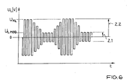
- den Verlauf der Schwingkreisspannungen UL, UC1; UC2
- Fig. 6
- ein gewünschtes Modulationsverhalten
- Fig. 1
- a transmitting and receiving resonant circuit with elements for load modulation for a first voltage half-wave
- Fig. 2
- the transmitting and receiving resonant circuit
Fig.1 with elements for load modulation for a second voltage half-wave - Fig. 3
- a further transmitting and receiving resonant circuit with elements for load modulation for a first voltage half-wave
- Fig. 4
- the transmitting and receiving resonant circuit
Figure 3 with elements for load modulation for a second voltage half-wave - Fig. 5
- the course of the oscillatory circuit voltages U L , U C1 ; U C2
- Fig. 6
- a desired modulation behavior
Bei den Ausführungsbeispielen gemäß der
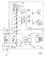
Ebenfalls parallel zum Schwingkreis 10 und zwischen dem ersten C1 25 und zweiten Schwingkreisanschluss C2 26, liegt eine Reihenschaltung aus Polaritätswechselschaltung 14 und Dioden 19, 20, 21, 22, 23, 24, die zur Ansteuerung des Sperrschichtbauteils 27 dienen. Hierbei können die Dioden als NMOS-Transistoren realisiert werden, die als Diode geschaltet sind. Parallel zum Sperrschichtbauteil 27 liegt weiterhin eine Gleichrichterschaltung 29 mit einem weiteren Bezugspotentialanschluss 30.
Die Polaritätswechselschaltung 14 besteht aus zwei parallelen Reihenschaltungen, die jeweils einem ohmschen Widerstand R1 15 bzw. R2 16 und eine Diode 17 bzw. 18 umfassen, wobei die Durchflussrichtung der Dioden 17, 18 unterschiedlich ist.
Die Dioden 19 bis 24 können durch Schalter S1 31, S2 32, S3 33 überbrückt werden, die von der Steuerschaltung 34 über kaskadierenden MOD-Signale MOD0, MOD1 und MOD2 betätigt werden. Die Schalter 31, 32, 33 werden bevorzugt als Transistoren, insbesondere als MOS-Transistoren realisiert.Also parallel to the
The
The
Das Sperrschichtbauteil 27 dient zunächst zur Begrenzung der Schwingkreisspannung UL 1 zwischen den Anschlüssen 25 und 26 des Sende- und Empfangsschwingkreises 10 bei offenen Schaltern 31, 32 und 33. In diesem Zustand begrenzt das Sperrschichtbauteil 27 jeweils dann, wenn der Potentialunterschied zwischen dem Bezugspotentialanschluss 28, 30 und einem der Anschlüsse 25 oder 26 die Durchlassspannung des Sperrschichtbauteils 27 überschreitet. Dieser Wert definiert die obere Begrenzungsspannung oder erste Klemmspannung UKL 2.2.
Beim Überbrücken der Dioden 19 bis 24 durch die Schalter 31, 32 und 33, wobei diese zur stufenförmigen Modulation der Spannung nacheinander und nicht zeitgleich geschlossen werden, klemmt das Sperrschichtbauteil 27 die Schwingkreisspannung UL 1 auf einen niedrigeren Wert ULMOD2.1.The
When bridging the
Durch Öffnen und Schließen der Schalter 31, 32, 33 moduliert die Steuerschaltung 34 den Wert der Schwingkreisspannung UL 1 entsprechend der zu übertragenden Datenfolge. Wie beschrieben bildet sich diese Modulation des Sende- und Empfangsschwingkreises 10 des tags als Modulation der Last des Sende- und Empfangsschwingkreises des Lesegeräts unter der Voraussetzung einer transformatorischen Kopplung.By opening and closing the
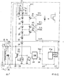
Das Sperrschichtbauteil 35 dient zur Begrenzung der Schwingkreisspannung UL 1 auf den Wert der oberen Klemmspannung UKL 2.2 zwischen den Anschlüssen 25 und 26 des Sende- und Empfangsschwingkreises 10. Wenn der Schalter S1 9 geschlossen ist, liegt am Sperrschichtbauteil 35 die Spannung Uref 3 an, die durch die vorgegebene Spannung UG 6 am Gate begrenzt wird und somit nicht über die Schwellspannung des PMOS-Transistors hinausgehen kann. Sobald der Schalter S1 9 mittels des nMOD 4 Signals der Steuerschaltung 34 geöffnet wird, wird der Kondensator 7 auf den Wert Uref 3aufgeladen und anschließend mittels des Entladestroms der Stromquelle lE2 8 entladen. Die Folge davon ist, dass die Spannung UG 6 am Gate linear auf null absinkt. Dadurch wird die Schwingkreisspannung UL 1 auf eine zweite, kleinere Klemmspannung ULMOD 2.1 begrenzt, die der Schwellspannung des PMOS-Transistors entspricht.The barrier layer component 35 is used to limit the resonant
Wenn UL 1 positiv ist, werden bei der Schaltung gemäß
When
- 11
- UL SchwingkreisspannungU L resonant circuit voltage
- 2.12.1
- ULMOD untere Klemmspannung (modulierte Spannung)UL MOD lower clamp voltage (modulated voltage)
- 2.22.2
- UKL obere KlemmspannungU KL upper clamping voltage
- 33
- Uref SpannungsreferenzU ref voltage reference
- 44
- nMOD inverses Signaln MOD inverse signal
- 5.15.1
- Modulationssignal MOD0 Modulation signal MOD 0
- 5.25.2
- Modulationssignal MOD1 Modulation signal MOD 1
- 5.35.3
- Modulationssignal MOD2 Modulation signal MOD 2
- 66
- UG GatespannungU G gate voltage
- 77
- C2 KondensatorC 2 capacitor
- 88th
- lE2 Stromquelle EntladestromlE 2 current source discharge current
- 99
- Schalter S1 Switch S 1
- 1010
- Sende - und EmpfangsschwingkreisTransmitting and receiving resonant circuit
- 1111
- TagDay
- 1212
- Induktivität LInductance L
- 1313
- Kapazität CCapacity C
- 1414
- PolaritätswechselschaltungPolarity reversal circuit
- 1515
- Ohmscher Widerstand R1Ohmic resistance R1
- 1616
- Ohmscher Widerstand R2Ohmic resistance R2
- 1717
- Diode bei R1Diode at R1
- 1818
- Diode bei R2Diode at R2
- 1919
- Diodediode
- 2020
- Diodediode
- 2121
- Diodediode
- 2222
- Diodediode
- 2323
- Diodediode
- 2424
- Diodediode
- 2525
- Erster Schwingkreisanschluss C1 First resonant circuit connection C 1
- 2626
- Zweiter Schwingkreisanschluss C2 Second resonant circuit connection C 2
- 2727
- Sperrschichtbauteil M1Barrier layer component M1
- 2828
- BezugspotentialanschlussReference potential terminal
- 2929
- GleichrichterschaltungRectifier circuit
- 3030
- BezugspotentialanschlussReference potential terminal
- 3131
- Schalter S1 Switch S 1
- 3232
- Schalter S2 Switch S 2
- 3333
- Schalter S3 Switch S 3
- 3434
- Steuerschaltung (Digital-Analog-Konverter)Control circuit (digital-to-analog converter)
- 3535
- Sperrschichtbauteil P1 Barrier layer component P 1
Claims (9)
dadurch gekennzeichnet, dass
die im Sende- und Empfangsschwingkreis (10) induzierte Wechselspannung auf einen ersten Spannungswert (2.1) begrenzt wird, indem der Steuereingang (27) des Sperrschichtbauelementes (P1) mittels eines Schalters (S1) mit einer Spannungsquelle (Uref3) verbunden wird.Method for limiting the voltage in a transponder having a first transmitting and receiving resonant circuit (10), which has a first oscillating circuit connection (25) and a second oscillating circuit connection (26), wherein
characterized in that
the alternating voltage induced in the transmitting and receiving resonant circuit (10) is limited to a first voltage value (2.1) by connecting the control input (27) of the junction device (P1) to a voltage source (Uref3) by means of a switch (S1).
dadurch gekennzeichnet, dass
durch Öffnen des Schalters (S1) der Steuereingang (27) von der Spannungsquelle (Uref3) getrennt wird sodass die induzierte Wechselspannung auf einen zweiten Spannungswert (2.2), der kleiner als der erste Spannungswert ist, begrenzt wird.Method according to claim 1,
characterized in that
by opening the switch (S1) the control input (27) is disconnected from the voltage source (Uref3) so that the induced AC voltage is limited to a second voltage value (2.2), which is smaller than the first voltage value.
dadurch gekennzeichnet, dass
zur Lastmodulation die Spannung abwechselnd zwischen dem zweiten Spannungswert (2.2) und dem ersten Spannungswert (2.1) begrenzt wird.Method according to claim 2,
characterized in that
for load modulation, the voltage is alternately limited between the second voltage value (2.2) and the first voltage value (2.1).
dadurch gekennzeichnet, dass
die Änderung von dem zweiten Spannungswert (2.2) auf dem ersten Spannungswert (2.1) kontinuierlich erfolgt, indem nach dem Trennen von der Spannungsquelle (Uref3) ein mit dem Steuereingang (27) verbundenes Speicherelement (C2) entladen wird.Method according to claim 2 or claim 3,
characterized in that
the change from the second voltage value (2.2) to the first voltage value (2.1) takes place continuously by discharging a storage element (C2) connected to the control input (27) after disconnection from the voltage source (Uref3).
dadurch gekennzeichnet, dass
eine stufenlose Modulation durchgeführt wird, indem das Speicherelement (C2) von einer Steuerschaltung (34) mittels des Schalters (S1) mit der Spannungsquelle (Uref3) verbunden und getrennt wird.Method according to one of the claims 4,
characterized in that
a continuous modulation is performed by the storage element (C2) by a control circuit (34) by means of the switch (S1) to the voltage source (Uref3) connected and disconnected.
zur Begrenzung der induzierten Wechselspannung auf einen ersten Spannungswert (2.1) der Steuereingang (27 mittels eines Schalters (S1) mit einer Spannungsquelle (Uref3) verschaltet ist.Circuit for limiting the voltage in a transponder having a first transmitting and receiving resonant circuit (10) having a first resonant circuit terminal (25) and a second resonant circuit terminal (26), wherein
for limiting the induced AC voltage to a first voltage value (2.1), the control input (27 is interconnected by means of a switch (S1) with a voltage source (Uref3).
dadurch gekennzeichnet, dass
der Schalter (S1) mit einem Steuereingang vorgesehen ist und an dem Steuereingang des Schalters (S1) eine Spannung (nMOD) einer Steuerschaltung (34) anliegt, und wobei der Schalter (S1) mittels der Spannung (nMOD) die Spannungsquelle (Uref3) mit dem Steuereingang (27) des Sperrschichtbauelementes (P1) verbindet oder trennt.Circuit according to one of Claims 6,
characterized in that
the switch (S1) is provided with a control input and to the control input of the switch (S1) a voltage (nMOD) of a control circuit (34) is applied, and wherein the switch (S1) by means of the voltage (nMOD) the voltage source (Uref3) with the control input (27) of the junction device (P1) connects or disconnects.
dadurch gekennzeichnet, dass
zwischen dem Steuereingang (27) und dem Schalter (S1) ein Kondensator (C2) in Parallelschaltung vorgesehen ist.Circuit according to claim 7,
characterized in that
between the control input (27) and the switch (S1), a capacitor (C2) is provided in parallel.
dadurch gekennzeichnet, dass
zum Entladen des Kondensators (C2) zwischen dem Steuereingang (27) und dem Kondensator (C2) eine Stromquelle (8) vorgesehen ist.A circuit according to claim 8 or claim 7,
characterized in that
for discharging the capacitor (C2) between the control input (27) and the capacitor (C2) a current source (8) is provided.
Applications Claiming Priority (2)
| Application Number | Priority Date | Filing Date | Title |
|---|---|---|---|
| DE200610006912 DE102006006912A1 (en) | 2006-02-15 | 2006-02-15 | Transponder`s voltage limiting method for radio frequency identification application, involves controlling control terminal of barrier component by voltage of terminals of oscillating circuit for limiting voltage in oscillating circuit |
| EP07002790A EP1821405B1 (en) | 2006-02-15 | 2007-02-09 | Method for voltage limitation for a transponder |
Related Parent Applications (2)
| Application Number | Title | Priority Date | Filing Date |
|---|---|---|---|
| EP07002790.9 Division | 2007-02-09 | ||
| EP07002790A Division EP1821405B1 (en) | 2006-02-15 | 2007-02-09 | Method for voltage limitation for a transponder |
Publications (2)
| Publication Number | Publication Date |
|---|---|
| EP2139109A1 true EP2139109A1 (en) | 2009-12-30 |
| EP2139109B1 EP2139109B1 (en) | 2011-01-12 |
Family
ID=37948075
Family Applications (2)
| Application Number | Title | Priority Date | Filing Date |
|---|---|---|---|
| EP09009622A Active EP2139109B1 (en) | 2006-02-15 | 2007-02-09 | Method for voltage limitation for a transponder |
| EP07002790A Active EP1821405B1 (en) | 2006-02-15 | 2007-02-09 | Method for voltage limitation for a transponder |
Family Applications After (1)
| Application Number | Title | Priority Date | Filing Date |
|---|---|---|---|
| EP07002790A Active EP1821405B1 (en) | 2006-02-15 | 2007-02-09 | Method for voltage limitation for a transponder |
Country Status (3)
| Country | Link |
|---|---|
| US (1) | US7710213B2 (en) |
| EP (2) | EP2139109B1 (en) |
| DE (2) | DE502007006276D1 (en) |
Cited By (1)
| Publication number | Priority date | Publication date | Assignee | Title |
|---|---|---|---|---|
| WO2016058687A1 (en) * | 2014-10-16 | 2016-04-21 | Giesecke & Devrient Gmbh | Secure element having a light emitting diode |
Families Citing this family (5)
| Publication number | Priority date | Publication date | Assignee | Title |
|---|---|---|---|---|
| KR101932519B1 (en) * | 2011-11-14 | 2018-12-27 | 삼성전자 주식회사 | Apparatus and method for selecting picc in portable terminal |
| FR3023434B1 (en) * | 2014-07-02 | 2017-10-13 | Stmicroelectronics Rousset | VOLTAGE AND POWER LIMITER FOR ELECTROMAGNETIC TRANSPONDER |
| EP2963587B1 (en) * | 2014-07-04 | 2017-03-15 | Nxp B.V. | Voltage converter |
| JP2017063300A (en) * | 2015-09-24 | 2017-03-30 | エスアイアイ・セミコンダクタ株式会社 | Input circuit |
| US9919677B2 (en) * | 2015-12-03 | 2018-03-20 | Nxp B.V. | Integrated circuit device and method for dual-mode transponder communication protocol |
Citations (4)
| Publication number | Priority date | Publication date | Assignee | Title |
|---|---|---|---|---|
| US5815355A (en) * | 1997-10-06 | 1998-09-29 | Atmel Corporation | Modulation compensated clamp circuit |
| US20040099738A1 (en) * | 2002-11-21 | 2004-05-27 | Hewlett-Packard Development Company, L.P. | Memory tag and a reader |
| US20050156710A1 (en) * | 2002-02-01 | 2005-07-21 | Helmut Kranabenter | Adapting coil voltage of a tag to field strength |
| EP1589656A1 (en) * | 2004-04-22 | 2005-10-26 | ATMEL Germany GmbH | Circuit for and method of load modulation in a system comprising a transmit resonant circuit and a receive resonant circuit |
Family Cites Families (3)
| Publication number | Priority date | Publication date | Assignee | Title |
|---|---|---|---|---|
| FR2776865B1 (en) * | 1998-03-31 | 2000-05-05 | Commissariat Energie Atomique | INDUCTIVE COUPLING TELETRANSMISSION DEVICE |
| WO1999057681A1 (en) | 1998-05-05 | 1999-11-11 | Koninklijke Philips Electronics N.V. | Data carrier having rectifier means and having improved voltage limiting means |
| DE10301451A1 (en) * | 2003-01-10 | 2004-07-22 | Atmel Germany Gmbh | Wireless data transmission method between base station and transponder, by modulating electromagnet waves at receiver using modulation technique based on received field strength |
-
2007
- 2007-02-09 DE DE502007006276T patent/DE502007006276D1/en active Active
- 2007-02-09 DE DE502007002450T patent/DE502007002450D1/en active Active
- 2007-02-09 EP EP09009622A patent/EP2139109B1/en active Active
- 2007-02-09 EP EP07002790A patent/EP1821405B1/en active Active
- 2007-02-15 US US11/706,403 patent/US7710213B2/en active Active
Patent Citations (5)
| Publication number | Priority date | Publication date | Assignee | Title |
|---|---|---|---|---|
| US5815355A (en) * | 1997-10-06 | 1998-09-29 | Atmel Corporation | Modulation compensated clamp circuit |
| US20050156710A1 (en) * | 2002-02-01 | 2005-07-21 | Helmut Kranabenter | Adapting coil voltage of a tag to field strength |
| US20040099738A1 (en) * | 2002-11-21 | 2004-05-27 | Hewlett-Packard Development Company, L.P. | Memory tag and a reader |
| EP1589656A1 (en) * | 2004-04-22 | 2005-10-26 | ATMEL Germany GmbH | Circuit for and method of load modulation in a system comprising a transmit resonant circuit and a receive resonant circuit |
| DE102004020816A1 (en) | 2004-04-22 | 2005-11-17 | Atmel Germany Gmbh | Method and circuit for load modulation in a connection of a transmitting oscillating circuit and a receiving resonant circuit |
Non-Patent Citations (2)
| Title |
|---|
| "Circuitry for a wireless micorsystem for neural recording microprobes", ANNUAL INTERNATIONAL CONFERENCE OF THE IEEE ENGINEERING, vol. 1, 23 October 2001 (2001-10-23), pages 761 - 764 |
| RAO YU ET AL: "Circuitry for a wireless microsystem for neural recording microprobes", PROCEEDINGS OF THE 23RD. ANNUAL INTERNATIONAL CONFERENCE OF THE IEEE ENGINEERING IN MEDICINE AND BIOLOGY SOCIETY. 2001 CONFERENCE PROCEEDINGS. (EMBS). INSTANBUL, TURKEY, OCT. 25 - 28, 2001, ANNUAL INTERNATIONAL CONFERENCE OF THE IEEE ENGINEERING IN M, vol. VOL. 1 OF 4. CONF. 23, 25 October 2001 (2001-10-25), pages 761 - 764, XP010593486 * |
Cited By (2)
| Publication number | Priority date | Publication date | Assignee | Title |
|---|---|---|---|---|
| WO2016058687A1 (en) * | 2014-10-16 | 2016-04-21 | Giesecke & Devrient Gmbh | Secure element having a light emitting diode |
| US10231299B2 (en) | 2014-10-16 | 2019-03-12 | Giesecke+Devrient Mobile Security Gmbh | Secure element having a light emitting diode |
Also Published As
| Publication number | Publication date |
|---|---|
| EP1821405B1 (en) | 2009-12-30 |
| DE502007002450D1 (en) | 2010-02-11 |
| US7710213B2 (en) | 2010-05-04 |
| US20070194928A1 (en) | 2007-08-23 |
| EP2139109B1 (en) | 2011-01-12 |
| DE502007006276D1 (en) | 2011-02-24 |
| EP1821405A1 (en) | 2007-08-22 |
Similar Documents
| Publication | Publication Date | Title |
|---|---|---|
| EP1437816B1 (en) | Circuit arrangement for providing electric power from an eletromagnetic field | |
| EP1821405B1 (en) | Method for voltage limitation for a transponder | |
| EP1589656A1 (en) | Circuit for and method of load modulation in a system comprising a transmit resonant circuit and a receive resonant circuit | |
| DE102006035582B4 (en) | Vibration maintenance circuit for half-duplex transponder | |
| DE10301451A1 (en) | Wireless data transmission method between base station and transponder, by modulating electromagnet waves at receiver using modulation technique based on received field strength | |
| DE102007004843A1 (en) | Concept for providing a supply voltage and a load modulation in a transponder | |
| DE69936439T2 (en) | Capacitive modulation in an electromagnetic transponder | |
| DE112019002703T5 (en) | DEVICE FOR CONTACTLESS POWER TRANSFER | |
| DE112019001196T5 (en) | CONTACTLESS ENERGY TRANSFER DEVICE | |
| DE10393465T5 (en) | Current integrating sense amplifier for memory modules in RFID | |
| DE112019000704T5 (en) | NON-CONTACT POWER SUPPLY DEVICE | |
| EP1056039A2 (en) | Transmitter and receiver | |
| DE19602316C1 (en) | Device for transmitting data or energy | |
| DE102014208880B4 (en) | Driver circuit for an inductance and active transmitting device with a driver circuit | |
| EP1745405B1 (en) | Transmission circuit for a transponder system used for transmitting a digital signal via a transmit antenna | |
| EP0945829B1 (en) | Arrangement for a resonant circuit coil for contactless communicationsystems | |
| DE2504785C3 (en) | Circuit arrangement for the floating transmission of signals via isolating points in telecommunications systems | |
| EP2151067B1 (en) | Inductive transmission device for electrical energy and data | |
| DE102006006912A1 (en) | Transponder`s voltage limiting method for radio frequency identification application, involves controlling control terminal of barrier component by voltage of terminals of oscillating circuit for limiting voltage in oscillating circuit | |
| EP3113081A1 (en) | Radio transponder and method for tuning a radio transponder | |
| DE112018002607T5 (en) | CONTACTLESS ENERGY SUPPLY DEVICE | |
| DE102014009934B4 (en) | Energy transformer, gate driver and method | |
| EP1168626B1 (en) | Method for reducing the settling and rise times in oscillating circuits | |
| DE10250396B4 (en) | A device for generating electromagnetic waves, method for operating such a device and method for modulating the electromagnetic waves to be generated by such a device in accordance with data to be transmitted | |
| DE102014220394B4 (en) | Transponder arrangement and method for operating a transponder |
Legal Events
| Date | Code | Title | Description |
|---|---|---|---|
| PUAI | Public reference made under article 153(3) epc to a published international application that has entered the european phase |
Free format text: ORIGINAL CODE: 0009012 |
|
| AC | Divisional application: reference to earlier application |
Ref document number: 1821405 Country of ref document: EP Kind code of ref document: P |
|
| AK | Designated contracting states |
Kind code of ref document: A1 Designated state(s): DE FR |
|
| 17P | Request for examination filed |
Effective date: 20100325 |
|
| RIC1 | Information provided on ipc code assigned before grant |
Ipc: H03G 11/00 20060101ALI20100504BHEP Ipc: G06K 19/07 20060101ALI20100504BHEP Ipc: H04B 5/02 20060101ALI20100504BHEP Ipc: H03G 11/02 20060101AFI20100504BHEP |
|
| GRAP | Despatch of communication of intention to grant a patent |
Free format text: ORIGINAL CODE: EPIDOSNIGR1 |
|
| GRAS | Grant fee paid |
Free format text: ORIGINAL CODE: EPIDOSNIGR3 |
|
| GRAA | (expected) grant |
Free format text: ORIGINAL CODE: 0009210 |
|
| AC | Divisional application: reference to earlier application |
Ref document number: 1821405 Country of ref document: EP Kind code of ref document: P |
|
| AK | Designated contracting states |
Kind code of ref document: B1 Designated state(s): DE FR |
|
| REF | Corresponds to: |
Ref document number: 502007006276 Country of ref document: DE Date of ref document: 20110224 Kind code of ref document: P |
|
| REG | Reference to a national code |
Ref country code: DE Ref legal event code: R096 Ref document number: 502007006276 Country of ref document: DE Effective date: 20110224 |
|
| PLBE | No opposition filed within time limit |
Free format text: ORIGINAL CODE: 0009261 |
|
| STAA | Information on the status of an ep patent application or granted ep patent |
Free format text: STATUS: NO OPPOSITION FILED WITHIN TIME LIMIT |
|
| 26N | No opposition filed |
Effective date: 20111013 |
|
| REG | Reference to a national code |
Ref country code: FR Ref legal event code: ST Effective date: 20111125 |
|
| PG25 | Lapsed in a contracting state [announced via postgrant information from national office to epo] |
Ref country code: FR Free format text: LAPSE BECAUSE OF NON-PAYMENT OF DUE FEES Effective date: 20110314 |
|
| REG | Reference to a national code |
Ref country code: DE Ref legal event code: R097 Ref document number: 502007006276 Country of ref document: DE Effective date: 20111013 |
|
| REG | Reference to a national code |
Ref country code: DE Ref legal event code: R081 Ref document number: 502007006276 Country of ref document: DE Owner name: ATMEL CORP., SAN JOSE, US Free format text: FORMER OWNER: ATMEL AUTOMOTIVE GMBH, 74072 HEILBRONN, DE Effective date: 20130529 Ref country code: DE Ref legal event code: R082 Ref document number: 502007006276 Country of ref document: DE Representative=s name: GRUENECKER PATENT- UND RECHTSANWAELTE PARTG MB, DE Effective date: 20130529 Ref country code: DE Ref legal event code: R082 Ref document number: 502007006276 Country of ref document: DE Representative=s name: GRUENECKER, KINKELDEY, STOCKMAIR & SCHWANHAEUS, DE Effective date: 20130529 Ref country code: DE Ref legal event code: R081 Ref document number: 502007006276 Country of ref document: DE Owner name: ATMEL CORP., US Free format text: FORMER OWNER: ATMEL AUTOMOTIVE GMBH, 74072 HEILBRONN, DE Effective date: 20130529 |
|
| PGFP | Annual fee paid to national office [announced via postgrant information from national office to epo] |
Ref country code: DE Payment date: 20230119 Year of fee payment: 17 |
|
| P01 | Opt-out of the competence of the unified patent court (upc) registered |
Effective date: 20230528 |