EP2139053A1 - Current limiting device - Google Patents
Current limiting device Download PDFInfo
- Publication number
- EP2139053A1 EP2139053A1 EP08305352A EP08305352A EP2139053A1 EP 2139053 A1 EP2139053 A1 EP 2139053A1 EP 08305352 A EP08305352 A EP 08305352A EP 08305352 A EP08305352 A EP 08305352A EP 2139053 A1 EP2139053 A1 EP 2139053A1
- Authority
- EP
- European Patent Office
- Prior art keywords
- current limiting
- limiting unit
- current
- superconducting elements
- cooling medium
- Prior art date
- Legal status (The legal status is an assumption and is not a legal conclusion. Google has not performed a legal analysis and makes no representation as to the accuracy of the status listed.)
- Granted
Links
Images

Classifications
-
- H—ELECTRICITY
- H10—SEMICONDUCTOR DEVICES; ELECTRIC SOLID-STATE DEVICES NOT OTHERWISE PROVIDED FOR
- H10N—ELECTRIC SOLID-STATE DEVICES NOT OTHERWISE PROVIDED FOR
- H10N60/00—Superconducting devices
- H10N60/30—Devices switchable between superconducting and normal states
Definitions
- the present invention relates to an improved arrangement of superconducting elements in a current limiting device in particularly optimized for high voltage applications. Further, the present invention relates to such a current limiting device which can be easily adapted to the particular requirements of a specific application such as specific voltage level of said application etc.
- Superconductors offer a great potential as resistive fault current limiters which enable rapid and effective current limitation, automatic recovery and negligible impedance during normal operation. They are especially an enabling technology for other superconducting applications in the high voltage technology, for example superconducting cables.
- a superconducting fault current limiter comprises one or more superconducting elements housed in an insulating housing such as a cryostat, filled with a cooling medium for cooling the superconducting elements below their critical temperature Tc at which they exhibit superconducting properties.
- the critical temperature depends on the specific superconducting material.
- Suitable cooling mediums are for example nitrogen, helium, neon, hydrogen or mixtures thereof in their liquid state.
- Preferred superconducting materials are the high temperature superconductors such as BSCCO (bismuth-strontium-calcium-copper-oxide) and YBCO (yttrium-barium-copper-oxide) which have a critical temperature in the range of 67 K and 110 K.
- BSCCO bismuth-strontium-calcium-copper-oxide
- YBCO yttrium-barium-copper-oxide
- the first parameter is the nominal current at which the system will be operated as well as the limitation level at which the system shall limit the current.
- the superconducting elements must be selected in view of their current carrying capacity as well as in view of their limitation properties. In order to meet these requirements either one superconducting element or two or more superconducting elements electrically connected in parallel, may be necessary.
- the second parameter is the voltage level at which the current limiter shall be operated. By the voltage level the necessary number of superconducting elements which have to be electrically connected in series is determined.
- Liquid nitrogen typically used as cooling medium, also has very good insulation properties and, thus, helps to provide electrical insulation within the fault current limiter.
- a fault current limiter comprising at least one current limiting unit, wherein the current limiting unit is arranged in the interior of an insulation housing and wherein the current limiting unit comprises one or more superconducting elements, wherein the current limiting unit forms a casing which spatially separate the superconducting elements from the surrounding interior of the insulation housing and wherein the fault current limiter comprises a first cooling medium circuit for cooling the superconducting elements within the current limiting unit and a second cooling medium circuit for supplying the surrounding interior of the insulating housing.
- the present invention relates to a current limiting unit encasing one or more superconducting elements and the use of such current limiting unit for the modular design of a fault current limiter.
- the present invention is based on the separation of the necessary cooling of the superconducting elements within a fault current limiter and the insulation material necessary for high voltage insulation.
- the present invention relates to a fault current limiter which can be variably designed by standardized current limiting units and modules allowing easy adaptation and design, respectively, of a fault current limiter for the specific requirements of different applications.
- any superconducting element suitable for fault current limiting application can be used.
- the superconducting element is made of a high temperature superconducting material, such as mentioned above.
- the shape of the superconducting element is not particularly restricted provided that it is suitable for the use in a fault current limiter.
- the superconducting element can be composed of a bulk material, for example, superconducting elements obtainable by a sintering or melt casting method.
- the superconducting element can be composed of a superconducting layer deposited onto a substrate, for example such as known as coated conductors wherein a thin-film of superconductor material is provided onto a substrate, typically made of metal, by physical vapor deposition, chemical vapor deposition or chemical solution deposition etc..
- the superconducting element has a cylindrical shape, such as a rod, tube or coil, or a plate shape.
- the superconducting element(s) are arranged within a current limiting unit which spatially separates the superconducting element(s) from the surrounding, typically the interior of an insulation housing such as a cryostat.
- a current supply is provided for connecting the superconducting elements within the current liming unit to the grid.
- the current supply is simultaneously used for feeding and discharging cooling medium to the current limiting unit.
- the current supply has a hollow interior such as a tube. The current supply extends through the current limiting unit into the interior of the current limiting unit to the superconducting elements. For allowing exchange of the cooling medium to and from the interior of the current limiting unit at the end portion of the current supply which is within the current limiting unit, an opening is provided.
- the current supplies 6a, b form part of the first cooling medium circuit which serves to cool the superconducting elements.
- the superconducting element is connected to a current supply at its opposing ends.
- the superconducting element(s) present within the current limiting unit can be arranged within a holder.
- the holder is suited to connect the superconducting elements electrically in parallel with each other. Simultaneously, by the holder the arrangement of superconducting elements electrically connected in parallel are connected electrically in serious within the system.
- the casing of the fault current limiting unit of the present invention can be formed by an electrically non conductive material.
- the casing is formed of a shielding electrode surrounding the superconducting elements with open faces, if any, being closed by an electrically non conductive cover or similar.
- the outer surface of the current limiting unit is essentially smooth and has an essentially round shape without square etches and spikes for avoiding accumulation of electrical charge which would promote flash over.
- the superconducting elements are substantially equal to each other.
- the current limiting unit of the present invention can be used as a standardized component for designing a standardized fault current limiter which can be easily adapted to the specific requirements of an intended application by varying the numbers of standardized current limiting units within the cryostat.
- a number of current limiting units are arranged within a cryostat and are connected electrically in series, for example, by the current supply connected to the individual current limiting units.
- cooling medium for supplying the surrounding interior of the insulation housing with cooling medium (second cooling medium circuit) any conventional supply system can be used which is generally known in the art.
- the holder 3 with the superconducting elements 2 is surrounded by shielding electrode 4 enclosing the superconducting elements 2 laterally and forming the bottom.
- shielding electrode 4 enclosing the superconducting elements 2 laterally and forming the bottom.
- the shielding electrode 4 can be formed of a sheet of an electrically conductive material such as a metal. Shielding electrodes and manufacturing thereof are in principle known.
- the shielding electrode 4 with the cover 5 forms a casing with at least the outer surface having an almost cylindrical shape.
- the lower and upper etch of the cylindrical body can be rounded by providing for example a tube 7 of electrically conductive material running along the circumference.
- the tube 7, also referred to "toroid” is made of the same material than the shielding electrode 4.
- tubular current supply tubes 6a, 6b are provided made of electrically conductive material, which are in electrical connection with the holder 3.
- each of the tubes 6a and 6b simultaneously serve to supply and discharge cooling medium into the current limiting unit 1.
- each of the tubes 6a and 6b has an opening 8 in its end portion extending between the bottom plate and top cover 5, respectively, and the holder 3.
- the openings 8 By means of the openings 8 the hollow interior of the supply tubes 6a, 6b and the chamber formed by the shielding electrode 4 and the cover 5 are in intercommunication.
- Holder 3 can be composed by an upper and an lower plate or stripe for holding the respective ends of the superconductor elements 2.
- the holder 3 can have the shape of a stripe or plate which is designed to hold the respective ends of the superconducting elements. To this, depressions can be provided in the holder having a shape fitting to the shape of the ends of the superconducting elements. The ends of the superconducting elements can be fixed to the holder, for example by soldering or similar.
- portions holding the ends can be designed to act as a clamping bush.
- suitable holders is generally known in the field of fault current limiters using superconducting elements.
- the holder 3 is designed to connect the individual superconducting elements 2 electrically in parallel and, simultaneously, to electrically connect the individual superconducting elements 2 with the supply tubes 6a and 6b, respectively.
- holder 3, or at least respective parts of holder 3, are made of electrically conductive material, such as a metal or metal alloy.
- an opening is provided for allowing the passage of the supply tubes 6a and 6b, respectively.
- the passage of the supply tubes through the opening is leak prove for avoiding leaking of the cooling medium or gas bubbles to the surrounding. According to need a suitable sealing can be provided.
- any gas bubbles formed in fault current event are entrapped within the current limiting unit 1 and can leave the unit only via openings 8 within supply tubes 6a, b.
- the overall current limiting unit is housed in an insulation housing indicated by reference number 9, such as a cryostat.
- the superconducting elements 2 preferably have an elongated shape such as a tape, tube, rod or similar.
- superconducting elements 2 within a unit 1 are almost identical.
- the maximal electrical voltage which can occur within the unit, corresponds to the voltage drop along the superconducting elements 2 and is generated between the superconducting elements 2 and the shielding electrode 4.
- the electrical overall potential of the unit is relieved over the distance between the unit and any adjacent conductive component such as, for example, further units or the grounded insulation housing.
- the interior of the insulation housing is provided with a homogeneous insulation material, such as liquid nitrogen. Since no formation of gas bubbles must be considered in the design of the fault current limiter a compact space saving arrangement is possible. Due to the provision of two different circuits for the cooling medium the design suitable for high voltage can be simplified.
- the voltage to be expected within the unit is only small since the length of the superconducting elements is limited and the shielding electrode 4 has the same potential as one end of the superconducting elements.
- the current limiting units of the present invention can be advantageously used in the design of a standardized modular current limiting device which is adapted to the specific requirements of an application.
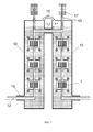
- FIG. 2 An example of such standardized modular current limiting device is shown in figure 2 wherein a plurality of current limiting units of the present invention are combined to form the desired current limiting device.
- the individual current limiting units are connected electrically in series by the supply tubes 6a, b which, simultaneously, serve to provide cooling medium to the interior of the current limiting units.
- two insulation housings 10 are coupled to each other via an upper docking site 13.
- the insulation housings 10 shown in figure 2 also comprise lower dockings sites 14 for coupling to further modular insulation housings (not shown).
- each insulation housing 10 The current limiting units in each insulation housing 10 are electrically connected by upper and lower electrical connection 11 and 12. Electrical connections 11 and 12, as the current supply 6 a, b, preferably have tubular shape for allowing communication of the cooling medium for the current limiting unit.
- Upper and lower electrical connection 12 are connected to current supply 6 a and 6 b.
- upper electrical connection 11 is connected to the upper end current supply 6 a of the upper end current limiting units of each of the insulation housings 10 coupled via upper docking site 13 and lower electrical connection 12 is connected to the lower end current supply 6 b of the lower end current limiting units of each of the insulation housings 10 coupled via lower docking site 14 (in figure 2 the further insulation housings coupled via lower docking site 12 are not shown).
- the individual modular insulation housings 10 form standardized modular components with the number being arranged in series being chosen according to need.
- the free electrical connection 11 or 12 (that is the electrical connection 11 or 12 which is not connected to a further module) can be used to connect the arrangement to an external grid.
- the respective docking site is tightly closed by a suitable, preferably releasable, closure.
- the endmost module can be modified by omitting the free electrical connection 11 and 12 and the respective docking sites and electrically connecting the arrangement to an external grid via the current supply 6 a and 6 b respectively, at the end of the series of modules 10 (free current supply).
- At least one discharge conduit 15 can be provided.
- the at least one discharge conduit 15 can be connected to the first cooling medium circuit at any suitable position.
- the discharge conduit is provided at a position on top of the first cooling medium circuit as shown in figure 2 .
- each modular insulation housing 10 is provided with a discharge conduit 15 wherein the discharge conduit 15 is connected to the upper end of the topmost supply 6a. Since the discharge conduit 15 is provided in a top position rising gas bubbles can be easily discharged.
- the discharge conduit 15 is made of an electrically non conductive material. Outside of the modular insulation housing 10 the discharge conduit 15 is provided with an outlet 17 such as a valve or the like, which allows escape of the gaseous cooling medium but prevents access from the outside into the first cooling circuit.
- Cooling medium can be, for example, supplied to the first cooling medium circuit via electrical connection 12, 13 at any free end or via discharge conduit 15.
- the top level of the liquid cooling medium within the cryostat housing 10 shall extend at least to the upper end of upper docking site 13 to ensure cooling of the docket site and the electrical connection therein.
- the interior of adjacent modules 10 can be linked via a compensation tube 14 allowing compensation of liquid, pressure etc. between the individual modules 10.
- modules 10 which can be coupled to each other.
- a further advantage of the present invention is that the junction from one module 10 to the adjacent module 10 via the docking sites 13, 14 allows connection in the cooled state. Thus, any loss of thermal energy is avoided as occurs in cases wherein successive insulation housings are connected via a warm connection extending outside the cooled interior.
Landscapes
- Emergency Protection Circuit Devices (AREA)
- Containers, Films, And Cooling For Superconductive Devices (AREA)
Abstract
Description
- The present invention relates to an improved arrangement of superconducting elements in a current limiting device in particularly optimized for high voltage applications. Further, the present invention relates to such a current limiting device which can be easily adapted to the particular requirements of a specific application such as specific voltage level of said application etc.
- Superconductors offer a great potential as resistive fault current limiters which enable rapid and effective current limitation, automatic recovery and negligible impedance during normal operation. They are especially an enabling technology for other superconducting applications in the high voltage technology, for example superconducting cables.
- Typically a superconducting fault current limiter comprises one or more superconducting elements housed in an insulating housing such as a cryostat, filled with a cooling medium for cooling the superconducting elements below their critical temperature Tc at which they exhibit superconducting properties.
The critical temperature depends on the specific superconducting material. Suitable cooling mediums are for example nitrogen, helium, neon, hydrogen or mixtures thereof in their liquid state. - Preferred superconducting materials are the high temperature superconductors such as BSCCO (bismuth-strontium-calcium-copper-oxide) and YBCO (yttrium-barium-copper-oxide) which have a critical temperature in the range of 67 K and 110 K.
Thus, for these materials liquid nitrogen can be used as cooling medium which is preferred in view of costs. - In the design of a fault current limiter two particular parameters must be taken in consideration.
- The first parameter is the nominal current at which the system will be operated as well as the limitation level at which the system shall limit the current.
- That is, the superconducting elements must be selected in view of their current carrying capacity as well as in view of their limitation properties.
In order to meet these requirements either one superconducting element or two or more superconducting elements electrically connected in parallel, may be necessary. - The second parameter is the voltage level at which the current limiter shall be operated. By the voltage level the necessary number of superconducting elements which have to be electrically connected in series is determined.
- In order to meet these parameters for any specific application a fault current limiter has to be individually designed. Thus, there is a need for a standardized design which allows easy adaption of a fault current limiter to the specific requirements of the respective application.
- Further, in a fault current limiter which is to be operated at middle or high voltage level, voltages up to several 100 kV can occur. For avoiding any damage it is necessary that even at such extreme voltage peaks no flash over takes place between the individual structural elements of the current limiter, for example between the superconducting element(s) and the jacket of the cryostat housing, which typically is grounded.
- Liquid nitrogen, typically used as cooling medium, also has very good insulation properties and, thus, helps to provide electrical insulation within the fault current limiter.
- However, there is a problem, that in fault event the superconducting element(s) are thermally heated up to temperatures exceeding the boiling temperature of the surrounding liquid nitrogen. In the result gaseous nitrogen, that is gas bubbles, are formed within the cryostat. However the electric insulation properties of gaseous nitrogen is significantly less than that of liquid nitrogen. In addition gaseous nitrogen not only has a less break through strength than liquid nitrogen but also leads to reduction of the electrical field in regions, where the liquid nitrogen is displaced by the gas bubbles, both factors enhancing the risk of flash over. Consequently, for avoiding voltage flash over the distances between the structural elements in the cryostat must be selected greater as would be the case of liquid nitrogen.
Consequently, the required space for the fault current limiter is enhanced. - In view of the above there is a need for a fault current limiter applying superconducting elements with a space saving arrangement suitable for high voltage application and which can be, nevertheless, safely operated.
- According to the present invention this problem is solved by a fault current limiter comprising at least one current limiting unit, wherein the current limiting unit is arranged in the interior of an insulation housing and wherein the current limiting unit comprises one or more superconducting elements, wherein the current limiting unit forms a casing which spatially separate the superconducting elements from the surrounding interior of the insulation housing and wherein the fault current limiter comprises a first cooling medium circuit for cooling the superconducting elements within the current limiting unit and a second cooling medium circuit for supplying the surrounding interior of the insulating housing.
- Further, the present invention relates to a current limiting unit encasing one or more superconducting elements and the use of such current limiting unit for the modular design of a fault current limiter.
- In a first aspect the present invention is based on the separation of the necessary cooling of the superconducting elements within a fault current limiter and the insulation material necessary for high voltage insulation.
- In a second aspect the present invention relates to a fault current limiter which can be variably designed by standardized current limiting units and modules allowing easy adaptation and design, respectively, of a fault current limiter for the specific requirements of different applications.
- For the present invention, in principle, any superconducting element suitable for fault current limiting application can be used.
Preferably, the superconducting element is made of a high temperature superconducting material, such as mentioned above. - Further, the shape of the superconducting element is not particularly restricted provided that it is suitable for the use in a fault current limiter.
Preferably, the superconducting element can be composed of a bulk material, for example, superconducting elements obtainable by a sintering or melt casting method.
Further, the superconducting element can be composed of a superconducting layer deposited onto a substrate, for example such as known as coated conductors wherein a thin-film of superconductor material is provided onto a substrate, typically made of metal, by physical vapor deposition, chemical vapor deposition or chemical solution deposition etc.. - Preferably, the superconducting element has a cylindrical shape, such as a rod, tube or coil, or a plate shape.
- According to the present invention the superconducting element(s) are arranged within a current limiting unit which spatially separates the superconducting element(s) from the surrounding, typically the interior of an insulation housing such as a cryostat.
- Further, a current supply is provided for connecting the superconducting elements within the current liming unit to the grid.
According to the present invention the current supply is simultaneously used for feeding and discharging cooling medium to the current limiting unit.
To this, the current supply has a hollow interior such as a tube. The current supply extends through the current limiting unit into the interior of the current limiting unit to the superconducting elements.
For allowing exchange of the cooling medium to and from the interior of the current limiting unit at the end portion of the current supply which is within the current limiting unit, an opening is provided. - Consequently, according to the present invention the current supplies 6a, b form part of the first cooling medium circuit which serves to cool the superconducting elements.
- Typically, the superconducting element is connected to a current supply at its opposing ends.
- The superconducting element(s) present within the current limiting unit can be arranged within a holder.
In case of two or more superconducting elements, preferably, the holder is suited to connect the superconducting elements electrically in parallel with each other. Simultaneously, by the holder the arrangement of superconducting elements electrically connected in parallel are connected electrically in serious within the system. - The casing of the fault current limiting unit of the present invention can be formed by an electrically non conductive material.
- According to a preferred embodiment the casing is formed of a shielding electrode surrounding the superconducting elements with open faces, if any, being closed by an electrically non conductive cover or similar. The outer surface of the current limiting unit is essentially smooth and has an essentially round shape without square etches and spikes for avoiding accumulation of electrical charge which would promote flash over.
- Preferably, within a current limiting unit the superconducting elements are substantially equal to each other.
- The current limiting unit of the present invention can be used as a standardized component for designing a standardized fault current limiter which can be easily adapted to the specific requirements of an intended application by varying the numbers of standardized current limiting units within the cryostat.
To this, according to need, a number of current limiting units are arranged within a cryostat and are connected electrically in series, for example, by the current supply connected to the individual current limiting units. - By the current limiting units of the present invention standardized components for the design of a fault current limiter are provided which allows not only a great but also a easy variation in the production of fault current limiters.
- Further, in fault event, gaseous cooling medium appears only within the current limiting unit, which spatially separates the superconducting elements from the surrounding interior of the insulation housing. Thus, escape of any gas bubbles into the surrounding interior of the insulation housing is prevented.
Since there are no gas bubbles within the surrounding interior of the insulation housing the insulation properties of the cooling medium, such as nitrogen, is not affected. Consequently in the design of the fault current limiter enhanced required space due to any decrease of insulation property must not be taken into consideration. Thus, the overall dimensions of the fault current limiter can be reduced compared to a conventional fault current limiter with occurrence of gas bubbles over the whole volume. - For supplying the surrounding interior of the insulation housing with cooling medium (second cooling medium circuit) any conventional supply system can be used which is generally known in the art.
- In the following the present invention is explained in further detail by reference to preferred embodiments shown in the figures.
- It is shown in
-
figure 1 schematically a longitudinal section of an embodiment of the current limiting unit of the present invention; and -
figure 2 schematically a longitudinal section of a modular assembly of a plurality of current limiting units of the present invention. - In the current limiting
unit 1 shown infigure 1 a plurality ofsuperconducting elements 2 are arranged in parallel within aholder 3. - The
holder 3 with thesuperconducting elements 2 is surrounded by shieldingelectrode 4 enclosing thesuperconducting elements 2 laterally and forming the bottom. By providing an upper cover 5 a casing is formed which is almost closed and which comprises theholder 3 with thesuperconducting elements 2. - The shielding
electrode 4 can be formed of a sheet of an electrically conductive material such as a metal. Shielding electrodes and manufacturing thereof are in principle known. The shieldingelectrode 4 with thecover 5 forms a casing with at least the outer surface having an almost cylindrical shape.
The lower and upper etch of the cylindrical body can be rounded by providing for example atube 7 of electrically conductive material running along the circumference. Preferably, thetube 7, also referred to "toroid", is made of the same material than the shieldingelectrode 4.
By the essentially cylindrical outer surface shape as well as by the provision of the toroids an essential rounded outer surface can be provided avoiding formation of square etches. - For electrical connection tubular current supply tubes 6a, 6b are provided made of electrically conductive material, which are in electrical connection with the
holder 3. - The current supply tubes 6a, 6b simultaneously serve to supply and discharge cooling medium into the current limiting
unit 1. To this, each of the tubes 6a and 6b has anopening 8 in its end portion extending between the bottom plate andtop cover 5, respectively, and theholder 3.
By means of theopenings 8 the hollow interior of the supply tubes 6a, 6b and the chamber formed by the shieldingelectrode 4 and thecover 5 are in intercommunication. - Each end of the same side of the
superconductor elements 2 is held byholder 3.
Holder 3 can be composed by an upper and an lower plate or stripe for holding the respective ends of thesuperconductor elements 2. - The
holder 3 can have the shape of a stripe or plate which is designed to hold the respective ends of the superconducting elements. To this, depressions can be provided in the holder having a shape fitting to the shape of the ends of the superconducting elements. The ends of the superconducting elements can be fixed to the holder, for example by soldering or similar. - Further, the portions holding the ends can be designed to act as a clamping bush. The design of suitable holders is generally known in the field of fault current limiters using superconducting elements.
- Preferably the
holder 3 is designed to connect the individualsuperconducting elements 2 electrically in parallel and, simultaneously, to electrically connect the individualsuperconducting elements 2 with the supply tubes 6a and 6b, respectively. To this,holder 3, or at least respective parts ofholder 3, are made of electrically conductive material, such as a metal or metal alloy. - In the bottom plate and cover 5 an opening is provided for allowing the passage of the supply tubes 6a and 6b, respectively.
Preferably, the passage of the supply tubes through the opening is leak prove for avoiding leaking of the cooling medium or gas bubbles to the surrounding.
According to need a suitable sealing can be provided. - According to the present invention any gas bubbles formed in fault current event are entrapped within the current limiting
unit 1 and can leave the unit only viaopenings 8 within supply tubes 6a, b. - The overall current limiting unit is housed in an insulation housing indicated by reference number 9, such as a cryostat.
- In the embodiment shown in
figure 1 thesuperconducting elements 2 preferably have an elongated shape such as a tape, tube, rod or similar.
Preferably,superconducting elements 2 within aunit 1 are almost identical. - The maximal electrical voltage, which can occur within the unit, corresponds to the voltage drop along the
superconducting elements 2 and is generated between thesuperconducting elements 2 and the shieldingelectrode 4. The electrical overall potential of the unit is relieved over the distance between the unit and any adjacent conductive component such as, for example, further units or the grounded insulation housing. - Since in the region between the unit and the jacket of the insulation housing (also referred to "surrounding interior") no gas bubbles are formed or present, the insulation effect of the cooling medium remains unchanged, and is not reduced. In the result the distances which must be kept are significantly lower than in case that formation of gas bubbles has to be considered.
- Due to the fact that between this region and the interior of the
unit 1 no or essentially no gas or liquid exchange is possible the interior of the insulation housing is provided with a homogeneous insulation material, such as liquid nitrogen. Since no formation of gas bubbles must be considered in the design of the fault current limiter a compact space saving arrangement is possible.
Due to the provision of two different circuits for the cooling medium the design suitable for high voltage can be simplified. - Further, the voltage to be expected within the unit is only small since the length of the superconducting elements is limited and the shielding
electrode 4 has the same potential as one end of the superconducting elements. - Consequently, according to the present invention due to the only low voltage drop within the unit and the different circuits of the cooling medium for the unit and the surrounding interior of the insulation housing the necessary dimensions in current limiter design can be significantly reduced, even for high voltage application, thus making possible the construction of a compact space keeping current limiting device.
- The current limiting units of the present invention can be advantageously used in the design of a standardized modular current limiting device which is adapted to the specific requirements of an application.
- An example of such standardized modular current limiting device is shown in
figure 2 wherein a plurality of current limiting units of the present invention are combined to form the desired current limiting device. - The individual current limiting units are connected electrically in series by the supply tubes 6a, b which, simultaneously, serve to provide cooling medium to the interior of the current limiting units.
- In the embodiment shown in
figure 2 two insulation housings 10 (in the following also referred to "modular insulation housing") are coupled to each other via anupper docking site 13.
Theinsulation housings 10 shown infigure 2 also compriselower dockings sites 14 for coupling to further modular insulation housings (not shown). - The current limiting units in each
insulation housing 10 are electrically connected by upper and lowerelectrical connection Electrical connections - Upper and lower
electrical connection 12 are connected to current supply 6 a and 6 b. - As shown in
figure 2 , for electrically connecting individualmodular insulation housings 10 electrically in series, upperelectrical connection 11 is connected to the upper end current supply 6 a of the upper end current limiting units of each of theinsulation housings 10 coupled viaupper docking site 13 and lowerelectrical connection 12 is connected to the lower end current supply 6 b of the lower end current limiting units of each of theinsulation housings 10 coupled via lower docking site 14 (infigure 2 the further insulation housings coupled vialower docking site 12 are not shown). - The individual
modular insulation housings 10, form standardized modular components with the number being arranged in series being chosen according to need. - In the
endmost module 10 the freeelectrical connection 11 or 12 (that is theelectrical connection - Alternatively, the endmost module can be modified by omitting the free
electrical connection - For discharging the gaseous cooling medium, i. e. the gas bubbles, from the first cooling circuit at least one
discharge conduit 15 can be provided. The at least onedischarge conduit 15 can be connected to the first cooling medium circuit at any suitable position.
Preferably the discharge conduit is provided at a position on top of the first cooling medium circuit as shown infigure 2 .
According tofigure 2 eachmodular insulation housing 10 is provided with adischarge conduit 15 wherein thedischarge conduit 15 is connected to the upper end of the topmost supply 6a. Since thedischarge conduit 15 is provided in a top position rising gas bubbles can be easily discharged. Thedischarge conduit 15 is made of an electrically non conductive material.
Outside of themodular insulation housing 10 thedischarge conduit 15 is provided with anoutlet 17 such as a valve or the like, which allows escape of the gaseous cooling medium but prevents access from the outside into the first cooling circuit. - Cooling medium can be, for example, supplied to the first cooling medium circuit via
electrical connection discharge conduit 15. - As shown in
figure 2 the top level of the liquid cooling medium within thecryostat housing 10 shall extend at least to the upper end ofupper docking site 13 to ensure cooling of the docket site and the electrical connection therein. - The interior of
adjacent modules 10 can be linked via acompensation tube 14 allowing compensation of liquid, pressure etc. between theindividual modules 10. - There is no particular limitation of the number of
modules 10 which can be coupled to each other. Thus, it is possible to couple asmuch modules 10 to each other as is required for a specific application, for example in view of voltage level. - A further advantage of the present invention is that the junction from one
module 10 to theadjacent module 10 via thedocking sites - The present design of current limiting units and modules which can be standardized, offers a great variability in the production of current limiting devices due to the possible standardized modular construction.
- 1
- current limiting unit
- 2
- superconducting element
- 3
- holder
- 4
- shielding electrode
- 5
- cover
- 6 a, b
- current supply tube
- 7
- toroid
- 8
- opening
- 9
- insulation housing
- 10
- modular insulation housing
- 11
- upper electrical connection
- 12
- lower electrical connection
- 13
- upper docking site
- 14
- lower docking site
- 15
- cooling medium supply
- 16
- compensation tube
- 17
- outlet
Claims (14)
- Fault current limiter comprising at least one current limiting unit (1), wherein the current limiting unit (1) is arranged within the interior of an insulation housing (9, 10) and wherein the current limiting unit (1) comprises one or more superconducting elements (2), wherein the current limiting unit (1) forms a casing which spatially separate the superconducting elements 2 from the surrounding interior of the insulation housing (9, 10) and wherein the fault current limiter unit (1) comprises a first cooling medium circuit for cooling the superconducting elements (2) within the current limiting unit (1) and a second cooling medium circuit for supplying the surrounding interior of the insulation housing (9, 10).
- Fault current limiter according to claim 1, wherein the casing of the current limiting unit (1) is formed by a shielding electrode (3) with an optionally left open face being closed by a cover (5).
- Fault current limiter according to claim 1 or 2, wherein the individual superconducting elements (2) are held by a holder (3).
- Fault current limiter according to claim, 3 wherein the individual superconducting elements (2) within the current limiting unit (1) are connected electrically in parallel.
- Fault current limiter according to any of the preceding claims, wherein the current limiting units (1) within the insulation housing (9, 10) are connected electrically in series by current supply tubes (6 a) and (6 b).
- Fault current limiter according to claim 5, wherein the current supply tubes (6 a) and (6 b) serve to feed and discharge cooling medium to the current limiting units (1) within the first cooling medium circuit for cooling the superconducting elements (2) within the current limiting units.
- Fault current limiter according to any of the preceding claims, wherein the insulation housing (9, 10) comprises at least one docking site (13, 14) suitable for coupling the insulating housing (9, 10) to at least a further insulation housing (9, 10).
- Fault current limiter according to the preceding claims, wherein the interior of successive insulation housings (9, 10) are physically connected by a compensation tube (16).
- Fault current limiter according to any of the preceding claims, wherein at least one conduit (15) is connected with the first cooling medium circuit for allowing discharge of gaseous cooling medium.
- Current limiting unit (1) comprising one or more superconducting elements (2), wherein the current limiting unit (1) forms a casing which spatially separates the superconducting elements (2) from the surrounding.
- Current limiting unit (1) according to claim 10, wherein the casing is formed by a shielding electrode (4) and wherein an optionally left open face is closed by a cover (5).
- Current limiting unit according to claims 10 or 11, wherein current supplies (6 a, 6 b) are provided for electrically connecting the superconducting elements (2) to further current limiting units (1) and/or to an external grit.
- Current limiting unit according to any of the claims 10 to 12, wherein the current supplies (6 a) and (6 b) have a tubular shape for simultaneously feeding and discharging cooling medium to the interior of the current limiting units (1).
- Use of an insulation housing (9, 10) and/or a current limiting unit (1) as defined to any of the claims 1 to 13 in the modular design of a fault current limiter.
Priority Applications (6)
| Application Number | Priority Date | Filing Date | Title |
|---|---|---|---|
| AT08305352T ATE477592T1 (en) | 2008-06-27 | 2008-06-27 | CURRENT LIMITING DEVICE |
| ES08305352T ES2350024T3 (en) | 2008-06-27 | 2008-06-27 | CURRENT LIMITING DEVICE. |
| EP08305352A EP2139053B1 (en) | 2008-06-27 | 2008-06-27 | Current limiting device |
| DE602008002152T DE602008002152D1 (en) | 2008-06-27 | 2008-06-27 | Current limiting device |
| JP2009139099A JP2010016368A (en) | 2008-06-27 | 2009-06-10 | Current-limiting device |
| US12/489,051 US8264802B2 (en) | 2008-06-27 | 2009-06-22 | Current limiting device |
Applications Claiming Priority (1)
| Application Number | Priority Date | Filing Date | Title |
|---|---|---|---|
| EP08305352A EP2139053B1 (en) | 2008-06-27 | 2008-06-27 | Current limiting device |
Publications (2)
| Publication Number | Publication Date |
|---|---|
| EP2139053A1 true EP2139053A1 (en) | 2009-12-30 |
| EP2139053B1 EP2139053B1 (en) | 2010-08-11 |
Family
ID=39773895
Family Applications (1)
| Application Number | Title | Priority Date | Filing Date |
|---|---|---|---|
| EP08305352A Not-in-force EP2139053B1 (en) | 2008-06-27 | 2008-06-27 | Current limiting device |
Country Status (6)
| Country | Link |
|---|---|
| US (1) | US8264802B2 (en) |
| EP (1) | EP2139053B1 (en) |
| JP (1) | JP2010016368A (en) |
| AT (1) | ATE477592T1 (en) |
| DE (1) | DE602008002152D1 (en) |
| ES (1) | ES2350024T3 (en) |
Cited By (1)
| Publication number | Priority date | Publication date | Assignee | Title |
|---|---|---|---|---|
| EP2716797A4 (en) * | 2011-05-31 | 2014-10-29 | Furukawa Electric Co Ltd | OXIDE SUPERCONDUCTOR THIN FILM, SUPERCONDUCTING DEFECT CURRENT LIMITER, AND METHOD FOR MANUFACTURING OXIDE SUPERCONDUCTOR THIN FILM |
Families Citing this family (1)
| Publication number | Priority date | Publication date | Assignee | Title |
|---|---|---|---|---|
| SG195087A1 (en) * | 2011-05-24 | 2013-12-30 | Furukawa Electric Co Ltd | Superconducting element for superconducting current limiter, method for manufacturing superconducting element for superconducting current limiter, and superconducting current limiter |
Citations (5)
| Publication number | Priority date | Publication date | Assignee | Title |
|---|---|---|---|---|
| JPH04193024A (en) * | 1990-11-26 | 1992-07-13 | Furukawa Electric Co Ltd:The | Variable rated current superconducting current limiter |
| DE19520205A1 (en) * | 1995-06-01 | 1996-12-05 | Siemens Ag | Resistive current limiting device using high-T¶c¶Supraleitermaterial |
| EP1217708A1 (en) * | 2000-12-21 | 2002-06-26 | Abb Research Ltd. | Superconducting device |
| WO2005006455A1 (en) * | 2003-07-04 | 2005-01-20 | Rolls-Royce Plc | A fault current limiter |
| US20070204632A1 (en) * | 2006-03-06 | 2007-09-06 | Ron Lee | Multi-bath apparatus and method for cooling superconductors |
Family Cites Families (1)
| Publication number | Priority date | Publication date | Assignee | Title |
|---|---|---|---|---|
| JP4193024B2 (en) | 2001-11-19 | 2008-12-10 | 株式会社イノアックコーポレーション | Retard roller and manufacturing method thereof |
-
2008
- 2008-06-27 AT AT08305352T patent/ATE477592T1/en not_active IP Right Cessation
- 2008-06-27 EP EP08305352A patent/EP2139053B1/en not_active Not-in-force
- 2008-06-27 ES ES08305352T patent/ES2350024T3/en active Active
- 2008-06-27 DE DE602008002152T patent/DE602008002152D1/en active Active
-
2009
- 2009-06-10 JP JP2009139099A patent/JP2010016368A/en not_active Withdrawn
- 2009-06-22 US US12/489,051 patent/US8264802B2/en not_active Expired - Fee Related
Patent Citations (5)
| Publication number | Priority date | Publication date | Assignee | Title |
|---|---|---|---|---|
| JPH04193024A (en) * | 1990-11-26 | 1992-07-13 | Furukawa Electric Co Ltd:The | Variable rated current superconducting current limiter |
| DE19520205A1 (en) * | 1995-06-01 | 1996-12-05 | Siemens Ag | Resistive current limiting device using high-T¶c¶Supraleitermaterial |
| EP1217708A1 (en) * | 2000-12-21 | 2002-06-26 | Abb Research Ltd. | Superconducting device |
| WO2005006455A1 (en) * | 2003-07-04 | 2005-01-20 | Rolls-Royce Plc | A fault current limiter |
| US20070204632A1 (en) * | 2006-03-06 | 2007-09-06 | Ron Lee | Multi-bath apparatus and method for cooling superconductors |
Cited By (2)
| Publication number | Priority date | Publication date | Assignee | Title |
|---|---|---|---|---|
| EP2716797A4 (en) * | 2011-05-31 | 2014-10-29 | Furukawa Electric Co Ltd | OXIDE SUPERCONDUCTOR THIN FILM, SUPERCONDUCTING DEFECT CURRENT LIMITER, AND METHOD FOR MANUFACTURING OXIDE SUPERCONDUCTOR THIN FILM |
| US9105794B2 (en) | 2011-05-31 | 2015-08-11 | Furukawa Electric Co., Ltd. | Oxide superconductor thin film, superconducting fault current limiter, and method for manufacturing oxide superconductor thin film |
Also Published As
| Publication number | Publication date |
|---|---|
| US20100157499A1 (en) | 2010-06-24 |
| US8264802B2 (en) | 2012-09-11 |
| ES2350024T3 (en) | 2011-01-17 |
| EP2139053B1 (en) | 2010-08-11 |
| DE602008002152D1 (en) | 2010-09-23 |
| ATE477592T1 (en) | 2010-08-15 |
| JP2010016368A (en) | 2010-01-21 |
Similar Documents
| Publication | Publication Date | Title |
|---|---|---|
| US11488747B2 (en) | Superconducting power cable system | |
| US4994932A (en) | Superconducting current limiting apparatus | |
| CN107646158B (en) | Superconducting fault current limiter system and connection system suitable for superconducting tapes | |
| DE102007013350B4 (en) | Power supply with high-temperature superconductors for superconducting magnets in a cryostat | |
| JP5687548B2 (en) | Device with superconducting cable | |
| JPH09190847A (en) | Terminal for connecting a superconducting polyphase cable to an electric device at room temperature | |
| US8271061B2 (en) | Connection arrangement for two superconductor cables | |
| JP5190211B2 (en) | Resistive current limiter | |
| JP2010251713A (en) | Current limiting device | |
| EP2139053B1 (en) | Current limiting device | |
| EP1509972A1 (en) | Current lead for superconducting apparatus | |
| WO2019146269A1 (en) | Superconductive cable | |
| KR101620495B1 (en) | Arrangement for current limiting | |
| EP3370239B1 (en) | Superconducting cable terminal device | |
| GB2162712A (en) | Electrical switch | |
| US7531750B2 (en) | Power supply line for cryogenic electrical systems | |
| KR101224214B1 (en) | Electrical feedthrough for connection of a superconducting device with a device located in room temperature | |
| de Souza et al. | Development and testing of joints in high temperature superconducting power cable | |
| US20120208702A1 (en) | Composite with coated conductor | |
| JP2013143474A (en) | Superconducting magnet device and current lead for the same | |
| EP2472618A1 (en) | Superconducting resistive fault current limiter | |
| WO2025093885A1 (en) | Apparatus | |
| JPH1012058A (en) | Superconducting power transmission cable | |
| JP2008130860A (en) | Superconducting devices and current leads | |
| JPH04210730A (en) | Rated current variable type superconducting limiter |
Legal Events
| Date | Code | Title | Description |
|---|---|---|---|
| PUAI | Public reference made under article 153(3) epc to a published international application that has entered the european phase |
Free format text: ORIGINAL CODE: 0009012 |
|
| 17P | Request for examination filed |
Effective date: 20080627 |
|
| AK | Designated contracting states |
Kind code of ref document: A1 Designated state(s): AT BE BG CH CY CZ DE DK EE ES FI FR GB GR HR HU IE IS IT LI LT LU LV MC MT NL NO PL PT RO SE SI SK TR |
|
| AX | Request for extension of the european patent |
Extension state: AL BA MK RS |
|
| GRAP | Despatch of communication of intention to grant a patent |
Free format text: ORIGINAL CODE: EPIDOSNIGR1 |
|
| GRAS | Grant fee paid |
Free format text: ORIGINAL CODE: EPIDOSNIGR3 |
|
| GRAA | (expected) grant |
Free format text: ORIGINAL CODE: 0009210 |
|
| AK | Designated contracting states |
Kind code of ref document: B1 Designated state(s): AT BE BG CH CY CZ DE DK EE ES FI FR GB GR HR HU IE IS IT LI LT LU LV MC MT NL NO PL PT RO SE SI SK TR |
|
| REG | Reference to a national code |
Ref country code: GB Ref legal event code: FG4D |
|
| REG | Reference to a national code |
Ref country code: CH Ref legal event code: EP |
|
| AKX | Designation fees paid |
Designated state(s): AT BE BG CH CY CZ DE DK EE ES FI FR GB GR HR HU IE IS IT LI LT LU LV MC MT NL NO PL PT RO SE SI SK TR |
|
| REG | Reference to a national code |
Ref country code: IE Ref legal event code: FG4D |
|
| REF | Corresponds to: |
Ref document number: 602008002152 Country of ref document: DE Date of ref document: 20100923 Kind code of ref document: P |
|
| REG | Reference to a national code |
Ref country code: SE Ref legal event code: TRGR |
|
| REG | Reference to a national code |
Ref country code: NL Ref legal event code: VDEP Effective date: 20100811 |
|
| REG | Reference to a national code |
Ref country code: ES Ref legal event code: FG2A Effective date: 20110104 |
|
| LTIE | Lt: invalidation of european patent or patent extension |
Effective date: 20100811 |
|
| PG25 | Lapsed in a contracting state [announced via postgrant information from national office to epo] |
Ref country code: NO Free format text: LAPSE BECAUSE OF FAILURE TO SUBMIT A TRANSLATION OF THE DESCRIPTION OR TO PAY THE FEE WITHIN THE PRESCRIBED TIME-LIMIT Effective date: 20101111 Ref country code: AT Free format text: LAPSE BECAUSE OF FAILURE TO SUBMIT A TRANSLATION OF THE DESCRIPTION OR TO PAY THE FEE WITHIN THE PRESCRIBED TIME-LIMIT Effective date: 20100811 Ref country code: FI Free format text: LAPSE BECAUSE OF FAILURE TO SUBMIT A TRANSLATION OF THE DESCRIPTION OR TO PAY THE FEE WITHIN THE PRESCRIBED TIME-LIMIT Effective date: 20100811 Ref country code: LT Free format text: LAPSE BECAUSE OF FAILURE TO SUBMIT A TRANSLATION OF THE DESCRIPTION OR TO PAY THE FEE WITHIN THE PRESCRIBED TIME-LIMIT Effective date: 20100811 Ref country code: NL Free format text: LAPSE BECAUSE OF FAILURE TO SUBMIT A TRANSLATION OF THE DESCRIPTION OR TO PAY THE FEE WITHIN THE PRESCRIBED TIME-LIMIT Effective date: 20100811 |
|
| PG25 | Lapsed in a contracting state [announced via postgrant information from national office to epo] |
Ref country code: CY Free format text: LAPSE BECAUSE OF FAILURE TO SUBMIT A TRANSLATION OF THE DESCRIPTION OR TO PAY THE FEE WITHIN THE PRESCRIBED TIME-LIMIT Effective date: 20100811 Ref country code: HR Free format text: LAPSE BECAUSE OF FAILURE TO SUBMIT A TRANSLATION OF THE DESCRIPTION OR TO PAY THE FEE WITHIN THE PRESCRIBED TIME-LIMIT Effective date: 20100811 Ref country code: IS Free format text: LAPSE BECAUSE OF FAILURE TO SUBMIT A TRANSLATION OF THE DESCRIPTION OR TO PAY THE FEE WITHIN THE PRESCRIBED TIME-LIMIT Effective date: 20101211 Ref country code: PL Free format text: LAPSE BECAUSE OF FAILURE TO SUBMIT A TRANSLATION OF THE DESCRIPTION OR TO PAY THE FEE WITHIN THE PRESCRIBED TIME-LIMIT Effective date: 20100811 Ref country code: SI Free format text: LAPSE BECAUSE OF FAILURE TO SUBMIT A TRANSLATION OF THE DESCRIPTION OR TO PAY THE FEE WITHIN THE PRESCRIBED TIME-LIMIT Effective date: 20100811 Ref country code: BG Free format text: LAPSE BECAUSE OF FAILURE TO SUBMIT A TRANSLATION OF THE DESCRIPTION OR TO PAY THE FEE WITHIN THE PRESCRIBED TIME-LIMIT Effective date: 20101111 |
|
| RAP2 | Party data changed (patent owner data changed or rights of a patent transferred) |
Owner name: NEXANS |
|
| PG25 | Lapsed in a contracting state [announced via postgrant information from national office to epo] |
Ref country code: GR Free format text: LAPSE BECAUSE OF FAILURE TO SUBMIT A TRANSLATION OF THE DESCRIPTION OR TO PAY THE FEE WITHIN THE PRESCRIBED TIME-LIMIT Effective date: 20101112 Ref country code: LV Free format text: LAPSE BECAUSE OF FAILURE TO SUBMIT A TRANSLATION OF THE DESCRIPTION OR TO PAY THE FEE WITHIN THE PRESCRIBED TIME-LIMIT Effective date: 20100811 Ref country code: BE Free format text: LAPSE BECAUSE OF FAILURE TO SUBMIT A TRANSLATION OF THE DESCRIPTION OR TO PAY THE FEE WITHIN THE PRESCRIBED TIME-LIMIT Effective date: 20100811 |
|
| PG25 | Lapsed in a contracting state [announced via postgrant information from national office to epo] |
Ref country code: DK Free format text: LAPSE BECAUSE OF FAILURE TO SUBMIT A TRANSLATION OF THE DESCRIPTION OR TO PAY THE FEE WITHIN THE PRESCRIBED TIME-LIMIT Effective date: 20100811 |
|
| PG25 | Lapsed in a contracting state [announced via postgrant information from national office to epo] |
Ref country code: SK Free format text: LAPSE BECAUSE OF FAILURE TO SUBMIT A TRANSLATION OF THE DESCRIPTION OR TO PAY THE FEE WITHIN THE PRESCRIBED TIME-LIMIT Effective date: 20100811 Ref country code: EE Free format text: LAPSE BECAUSE OF FAILURE TO SUBMIT A TRANSLATION OF THE DESCRIPTION OR TO PAY THE FEE WITHIN THE PRESCRIBED TIME-LIMIT Effective date: 20100811 Ref country code: CZ Free format text: LAPSE BECAUSE OF FAILURE TO SUBMIT A TRANSLATION OF THE DESCRIPTION OR TO PAY THE FEE WITHIN THE PRESCRIBED TIME-LIMIT Effective date: 20100811 Ref country code: RO Free format text: LAPSE BECAUSE OF FAILURE TO SUBMIT A TRANSLATION OF THE DESCRIPTION OR TO PAY THE FEE WITHIN THE PRESCRIBED TIME-LIMIT Effective date: 20100811 |
|
| PLBE | No opposition filed within time limit |
Free format text: ORIGINAL CODE: 0009261 |
|
| STAA | Information on the status of an ep patent application or granted ep patent |
Free format text: STATUS: NO OPPOSITION FILED WITHIN TIME LIMIT |
|
| 26N | No opposition filed |
Effective date: 20110512 |
|
| PGFP | Annual fee paid to national office [announced via postgrant information from national office to epo] |
Ref country code: SE Payment date: 20110613 Year of fee payment: 4 |
|
| REG | Reference to a national code |
Ref country code: DE Ref legal event code: R097 Ref document number: 602008002152 Country of ref document: DE Effective date: 20110512 |
|
| PG25 | Lapsed in a contracting state [announced via postgrant information from national office to epo] |
Ref country code: MT Free format text: LAPSE BECAUSE OF FAILURE TO SUBMIT A TRANSLATION OF THE DESCRIPTION OR TO PAY THE FEE WITHIN THE PRESCRIBED TIME-LIMIT Effective date: 20100811 |
|
| PGFP | Annual fee paid to national office [announced via postgrant information from national office to epo] |
Ref country code: IT Payment date: 20110630 Year of fee payment: 4 |
|
| REG | Reference to a national code |
Ref country code: IE Ref legal event code: MM4A |
|
| PG25 | Lapsed in a contracting state [announced via postgrant information from national office to epo] |
Ref country code: IE Free format text: LAPSE BECAUSE OF NON-PAYMENT OF DUE FEES Effective date: 20110627 |
|
| PGFP | Annual fee paid to national office [announced via postgrant information from national office to epo] |
Ref country code: ES Payment date: 20120627 Year of fee payment: 5 |
|
| REG | Reference to a national code |
Ref country code: SE Ref legal event code: EUG |
|
| REG | Reference to a national code |
Ref country code: CH Ref legal event code: PL |
|
| REG | Reference to a national code |
Ref country code: CH Ref legal event code: PL |
|
| PG25 | Lapsed in a contracting state [announced via postgrant information from national office to epo] |
Ref country code: SE Free format text: LAPSE BECAUSE OF NON-PAYMENT OF DUE FEES Effective date: 20120628 Ref country code: IT Free format text: LAPSE BECAUSE OF NON-PAYMENT OF DUE FEES Effective date: 20120627 |
|
| PG25 | Lapsed in a contracting state [announced via postgrant information from national office to epo] |
Ref country code: CH Free format text: LAPSE BECAUSE OF NON-PAYMENT OF DUE FEES Effective date: 20120630 Ref country code: LI Free format text: LAPSE BECAUSE OF NON-PAYMENT OF DUE FEES Effective date: 20120630 Ref country code: MC Free format text: LAPSE BECAUSE OF NON-PAYMENT OF DUE FEES Effective date: 20110630 |
|
| PG25 | Lapsed in a contracting state [announced via postgrant information from national office to epo] |
Ref country code: LU Free format text: LAPSE BECAUSE OF NON-PAYMENT OF DUE FEES Effective date: 20110627 |
|
| PG25 | Lapsed in a contracting state [announced via postgrant information from national office to epo] |
Ref country code: TR Free format text: LAPSE BECAUSE OF FAILURE TO SUBMIT A TRANSLATION OF THE DESCRIPTION OR TO PAY THE FEE WITHIN THE PRESCRIBED TIME-LIMIT Effective date: 20100811 |
|
| PG25 | Lapsed in a contracting state [announced via postgrant information from national office to epo] |
Ref country code: HU Free format text: LAPSE BECAUSE OF FAILURE TO SUBMIT A TRANSLATION OF THE DESCRIPTION OR TO PAY THE FEE WITHIN THE PRESCRIBED TIME-LIMIT Effective date: 20100811 |
|
| REG | Reference to a national code |
Ref country code: ES Ref legal event code: FD2A Effective date: 20140707 |
|
| PG25 | Lapsed in a contracting state [announced via postgrant information from national office to epo] |
Ref country code: PT Free format text: LAPSE BECAUSE OF FAILURE TO SUBMIT A TRANSLATION OF THE DESCRIPTION OR TO PAY THE FEE WITHIN THE PRESCRIBED TIME-LIMIT Effective date: 20100811 |
|
| PG25 | Lapsed in a contracting state [announced via postgrant information from national office to epo] |
Ref country code: ES Free format text: LAPSE BECAUSE OF NON-PAYMENT OF DUE FEES Effective date: 20130628 |
|
| REG | Reference to a national code |
Ref country code: FR Ref legal event code: PLFP Year of fee payment: 9 |
|
| REG | Reference to a national code |
Ref country code: FR Ref legal event code: PLFP Year of fee payment: 10 |
|
| REG | Reference to a national code |
Ref country code: FR Ref legal event code: PLFP Year of fee payment: 11 |
|
| PGFP | Annual fee paid to national office [announced via postgrant information from national office to epo] |
Ref country code: DE Payment date: 20180625 Year of fee payment: 11 |
|
| PGFP | Annual fee paid to national office [announced via postgrant information from national office to epo] |
Ref country code: FR Payment date: 20180620 Year of fee payment: 11 |
|
| PGFP | Annual fee paid to national office [announced via postgrant information from national office to epo] |
Ref country code: GB Payment date: 20180620 Year of fee payment: 11 |
|
| REG | Reference to a national code |
Ref country code: DE Ref legal event code: R119 Ref document number: 602008002152 Country of ref document: DE |
|
| GBPC | Gb: european patent ceased through non-payment of renewal fee |
Effective date: 20190627 |
|
| PG25 | Lapsed in a contracting state [announced via postgrant information from national office to epo] |
Ref country code: DE Free format text: LAPSE BECAUSE OF NON-PAYMENT OF DUE FEES Effective date: 20200101 Ref country code: GB Free format text: LAPSE BECAUSE OF NON-PAYMENT OF DUE FEES Effective date: 20190627 |
|
| PG25 | Lapsed in a contracting state [announced via postgrant information from national office to epo] |
Ref country code: FR Free format text: LAPSE BECAUSE OF NON-PAYMENT OF DUE FEES Effective date: 20190630 |