EP2136550A2 - Image pickup - Google Patents
Image pickup Download PDFInfo
- Publication number
- EP2136550A2 EP2136550A2 EP09251563A EP09251563A EP2136550A2 EP 2136550 A2 EP2136550 A2 EP 2136550A2 EP 09251563 A EP09251563 A EP 09251563A EP 09251563 A EP09251563 A EP 09251563A EP 2136550 A2 EP2136550 A2 EP 2136550A2
- Authority
- EP
- European Patent Office
- Prior art keywords
- image pickup
- light
- near infrared
- color filter
- beams
- Prior art date
- Legal status (The legal status is an assumption and is not a legal conclusion. Google has not performed a legal analysis and makes no representation as to the accuracy of the status listed.)
- Ceased
Links
- 125000006850 spacer group Chemical group 0.000 claims abstract description 33
- 239000000758 substrate Substances 0.000 claims abstract description 19
- 230000000737 periodic effect Effects 0.000 claims description 8
- 239000012780 transparent material Substances 0.000 claims description 3
- 238000010586 diagram Methods 0.000 description 20
- 238000000034 method Methods 0.000 description 19
- 230000003287 optical effect Effects 0.000 description 18
- 230000005540 biological transmission Effects 0.000 description 12
- 238000004519 manufacturing process Methods 0.000 description 12
- 239000011521 glass Substances 0.000 description 9
- 239000007787 solid Substances 0.000 description 9
- 210000001508 eye Anatomy 0.000 description 8
- 239000000463 material Substances 0.000 description 7
- 239000004038 photonic crystal Substances 0.000 description 5
- 229920002120 photoresistant polymer Polymers 0.000 description 5
- 238000005530 etching Methods 0.000 description 4
- 230000004397 blinking Effects 0.000 description 3
- 150000001875 compounds Chemical class 0.000 description 3
- 230000006866 deterioration Effects 0.000 description 3
- 238000009792 diffusion process Methods 0.000 description 3
- 238000005516 engineering process Methods 0.000 description 3
- 239000003973 paint Substances 0.000 description 3
- VYPSYNLAJGMNEJ-UHFFFAOYSA-N Silicium dioxide Chemical compound O=[Si]=O VYPSYNLAJGMNEJ-UHFFFAOYSA-N 0.000 description 2
- BQCADISMDOOEFD-UHFFFAOYSA-N Silver Chemical compound [Ag] BQCADISMDOOEFD-UHFFFAOYSA-N 0.000 description 2
- 210000005252 bulbus oculi Anatomy 0.000 description 2
- 238000009826 distribution Methods 0.000 description 2
- 238000001312 dry etching Methods 0.000 description 2
- 238000012544 monitoring process Methods 0.000 description 2
- 238000000206 photolithography Methods 0.000 description 2
- 230000010287 polarization Effects 0.000 description 2
- 239000011347 resin Substances 0.000 description 2
- 229920005989 resin Polymers 0.000 description 2
- 229910052709 silver Inorganic materials 0.000 description 2
- 239000004332 silver Substances 0.000 description 2
- 208000031481 Pathologic Constriction Diseases 0.000 description 1
- 238000003491 array Methods 0.000 description 1
- 238000010367 cloning Methods 0.000 description 1
- 229910052681 coesite Inorganic materials 0.000 description 1
- 229910052906 cristobalite Inorganic materials 0.000 description 1
- 238000001514 detection method Methods 0.000 description 1
- 239000000428 dust Substances 0.000 description 1
- 238000000609 electron-beam lithography Methods 0.000 description 1
- 238000011156 evaluation Methods 0.000 description 1
- 210000003128 head Anatomy 0.000 description 1
- 230000001678 irradiating effect Effects 0.000 description 1
- 238000000059 patterning Methods 0.000 description 1
- 239000002244 precipitate Substances 0.000 description 1
- 238000007639 printing Methods 0.000 description 1
- 238000007789 sealing Methods 0.000 description 1
- 239000000377 silicon dioxide Substances 0.000 description 1
- 229910052682 stishovite Inorganic materials 0.000 description 1
- 230000001360 synchronised effect Effects 0.000 description 1
- PBCFLUZVCVVTBY-UHFFFAOYSA-N tantalum pentoxide Inorganic materials O=[Ta](=O)O[Ta](=O)=O PBCFLUZVCVVTBY-UHFFFAOYSA-N 0.000 description 1
- 229910052905 tridymite Inorganic materials 0.000 description 1
Images



Classifications
-
- A—HUMAN NECESSITIES
- A61—MEDICAL OR VETERINARY SCIENCE; HYGIENE
- A61B—DIAGNOSIS; SURGERY; IDENTIFICATION
- A61B5/00—Measuring for diagnostic purposes; Identification of persons
- A61B5/16—Devices for psychotechnics; Testing reaction times ; Devices for evaluating the psychological state
- A61B5/18—Devices for psychotechnics; Testing reaction times ; Devices for evaluating the psychological state for vehicle drivers or machine operators
-
- B—PERFORMING OPERATIONS; TRANSPORTING
- B82—NANOTECHNOLOGY
- B82Y—SPECIFIC USES OR APPLICATIONS OF NANOSTRUCTURES; MEASUREMENT OR ANALYSIS OF NANOSTRUCTURES; MANUFACTURE OR TREATMENT OF NANOSTRUCTURES
- B82Y20/00—Nanooptics, e.g. quantum optics or photonic crystals
-
- G—PHYSICS
- G02—OPTICS
- G02B—OPTICAL ELEMENTS, SYSTEMS OR APPARATUS
- G02B1/00—Optical elements characterised by the material of which they are made; Optical coatings for optical elements
- G02B1/002—Optical elements characterised by the material of which they are made; Optical coatings for optical elements made of materials engineered to provide properties not available in nature, e.g. metamaterials
- G02B1/005—Optical elements characterised by the material of which they are made; Optical coatings for optical elements made of materials engineered to provide properties not available in nature, e.g. metamaterials made of photonic crystals or photonic band gap materials
-
- G—PHYSICS
- G02—OPTICS
- G02B—OPTICAL ELEMENTS, SYSTEMS OR APPARATUS
- G02B3/00—Simple or compound lenses
- G02B3/0006—Arrays
- G02B3/0012—Arrays characterised by the manufacturing method
- G02B3/0018—Reflow, i.e. characterized by the step of melting microstructures to form curved surfaces, e.g. manufacturing of moulds and surfaces for transfer etching
-
- G—PHYSICS
- G02—OPTICS
- G02B—OPTICAL ELEMENTS, SYSTEMS OR APPARATUS
- G02B5/00—Optical elements other than lenses
- G02B5/20—Filters
-
- H—ELECTRICITY
- H04—ELECTRIC COMMUNICATION TECHNIQUE
- H04N—PICTORIAL COMMUNICATION, e.g. TELEVISION
- H04N23/00—Cameras or camera modules comprising electronic image sensors; Control thereof
- H04N23/20—Cameras or camera modules comprising electronic image sensors; Control thereof for generating image signals from infrared radiation only
-
- H—ELECTRICITY
- H04—ELECTRIC COMMUNICATION TECHNIQUE
- H04N—PICTORIAL COMMUNICATION, e.g. TELEVISION
- H04N23/00—Cameras or camera modules comprising electronic image sensors; Control thereof
- H04N23/50—Constructional details
- H04N23/54—Mounting of pick-up tubes, electronic image sensors, deviation or focusing coils
-
- H—ELECTRICITY
- H04—ELECTRIC COMMUNICATION TECHNIQUE
- H04N—PICTORIAL COMMUNICATION, e.g. TELEVISION
- H04N23/00—Cameras or camera modules comprising electronic image sensors; Control thereof
- H04N23/56—Cameras or camera modules comprising electronic image sensors; Control thereof provided with illuminating means
-
- A—HUMAN NECESSITIES
- A61—MEDICAL OR VETERINARY SCIENCE; HYGIENE
- A61B—DIAGNOSIS; SURGERY; IDENTIFICATION
- A61B5/00—Measuring for diagnostic purposes; Identification of persons
- A61B5/103—Measuring devices for testing the shape, pattern, colour, size or movement of the body or parts thereof, for diagnostic purposes
- A61B5/11—Measuring movement of the entire body or parts thereof, e.g. head or hand tremor or mobility of a limb
- A61B5/1103—Detecting muscular movement of the eye, e.g. eyelid movement
Definitions
- the present invention relates to an image pickup, and more particularly to an image pickup for use in the detection of the driving status of a driver, etc.
- a method of taking a face image of a driver by an image pickup camera built in a rear view mirror (hereinafter referred to as a rear view mirror built-in image pickup) is used to detect the status of the driver.
- a rear view mirror built-in image pickup Securely taking face images of a driver in a wide range of illuminance from day to night is necessary.
- a rear view mirror built-in image pickup adopting a near infrared pulse light projection method is already present to securely take face images of a driver from a low illuminance during night to a high illuminance during daytime.
- a light emission unit in which LEDs emitting light having a wavelength of 850 nm are arranged, an image pickup unit of a charge-coupled camera (CCD), etc are built-in a rear view mirror.
- the rear view mirror built-in image pickup irradiates an object (driver) with beams of near infrared having a wavelength of 850nm in a pulse manner during which the shutter of the CCD camera is open to receive a reflection light image.
- a near infrared bandpass filter mirror which transmits beams of near infrared and reflects optical light required for the driver is used to receive a reflection light image with the CCD camera formed by irradiating the driver with the beams of near infrared without a loss while not hindering the function of the rear view mirror.
- images of a driver are securely obtained by using near infrared.
- the object of detecting and monitoring the status of a driver during driving is to detect and monitor deterioration of consciousness due to dozing off, inattentive driving, etc.
- the rear view mirror built-in image pickup described above shoots a face image of a driver, takes out (detects) the face area and eye area from the face image, and measures blinks and the direction of the line of sight.
- the rear view mirror built-in image pickup detects the degree of deterioration of consciousness from the change in the time of shutting eyes of blinking and inattentive view from the direction of the face and/or the eyeball.
- the rear view mirror built-in image pickup can securely shoot face images of a driver in the environment in which the illuminance changes from day to night.
- the rear view mirror built-in image pickup employs a method of using only near infrared light having a single wavelength of 850 nm, placing the position of the face of a driver is limiting with regard to high precision.
- a near infrared multi-band image pickup uses near infrared light having a wavelength of 870 nm and near infrared having a wavelength of 970 nm.
- the near infrared multi-band image pickup irradiates the driver with near infrared having a wavelength of 870 nm and near infrared having a wavelength of 970 nm sequentially to obtain two images of 870 nm and 970 nm by a CCD camera.
- the image pickup detects the skin and hair portions by calculating the difference between the luminance values of the two irradiation images and discriminates the two portions from the symbol of the difference.
- the optical light is cut by an optical filter so that a secure image can be obtained.
- the near infrared multi-band image pickup makes it possible to place the face of man with high accuracy but since the infrared having a wavelength of 870 nm and the infrared having a wavelength of 970 nm are emitted sequentially, images should be obtained by sequential lighting in a synchronized manner, which causes problems with regard to complexity and real time property.
- the present inventor recognizes that a need exists for an image pickup which detects the driving status of a driver by placing the face portion of the driver with high precision and taking a face image in a real time manner.
- an object of the present invention is to provide an image pickup which detects the driving status of a driver by locating the face portion of the driver with high precision and extracting a face image in a real time manner.
- an image pickup including a light emission portion that irradiates an object with near infrared; and an image pickup portion that receives a reflection light image of the object by the near infrared.
- the image pickup portion includes a lens array containing a substrate on which multiple lenses to respectively receive the reflection light image of the object by the near infrared are arranged; a light shield spacer that shields beams of light that have passed through the lens array from each other; a color filter separated into areas according to beams of light that pass through the light shield spacer, each of which transmits only particular beams of near infrared depending on the wavelengths thereof; and an image pickup element that simultaneously obtains multiple images of the object which are formed of each of the particular beams of near infrared having independent wavelengths that have passed through each of the areas of the color filter.
- the color filter is a laminate structure in which, in an XYZ orthogonal coordinate system, at least two kinds of transparent materials are alternately arranged in the Z direction on a substrate arranged in parallel with the XY plane, each layer of the laminate structure has one dimensional periodic concavo-convex form repeated in one direction in the XY plane determined depending on each of the areas and the beams of light that pass through the light shield spacer enters into the XY plane.
- the color filter has a groove or lattice structure arranged on a substrate with a regular cycle.
- the image pickup element is installed on an image pickup element holder, a spacer having a rectangle frame is provided on the image pickup element holder, the color filter is installed on the spacer, and the image pickup element is sealed by the spacer, the color filter, and the image pickup element holder.
- infrared having a wavelength of 870 nm and infrared having a wavelength of 970 nm are used in the near infrared multi-band image pickup described above.
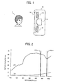
- Fig. 1 is a schematic diagram illustrating the entire structure of the image pickup related to a first embodiment of the present invention.
- a reference numeral 10 represents an image pickup unit such as a charge coupled device (CCD) that shoots a face image of a driver. 1 as the object
- a reference numeral 20 represents a light emission unit that irradiates the driver 1 with near infrared using an infrared LED.
- the image pickup unit 10 and the light emission unit 20 are built in a rear view mirror 50 of a car to obtain the face image of the driver without being affected by the driving operation.
- a near infrared bandpass filter 30 is provided on the front of the rear view mirror 50.
- the near infrared bandpass filter 30 transmits emitted near infrared and reflects optical light so that the near infrared is projected to the driver 1 without a loss and the reflection light is received at the image pickup unit 10 while avoiding hindrance of the function of the rear view mirror 50 by taking images of the driver 1.
- a controller (not shown) which controls the shutter speed and the gain of the camera in the image pickup unit 10, and the emission timing of the infrared LED of the light emission unit 20 is built in the rear view mirror 50.
- the light emission unit 20 emits near infrared in a pulse manner in synchronization with the image pickup timing determined by the controller (not shown). This near infrared passes through the near infrared bandpass filter 30 and is projected to the face portion of the driver 1. The reflection light passes through the near infrared bandpass filter 30 and is received on the image pickup unit 10 such as a CCD camera.
- the image pickup unit 10 separates the received near infrared into two beams of light via a lens array employing a compound eye system and each beam of light enters into a color filter separated into different areas depending on the transmission wavelength of 870 nm or 970 nm and then into the image pickup element such as a CCD.
- a color filter separated into different areas depending on the transmission wavelength of 870 nm or 970 nm and then into the image pickup element such as a CCD.
- a CCD camera can generally sense light beams having a wavelength of from 770 to 1,000 nm in the near infrared range.
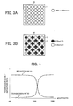
- the reflection characteristics of the face portion of a man in the near infrared range are known as illustrated in Fig. 2 .
- the reflection characteristics of the skin and the hair are opposite, i.e., diagonally right down and right up, respectively. Therefore, when calculating the difference between the two object images, the symbols of the difference are opposite depending on the skin or the hair.
- the skin and the hair are discernable by the difference of the two object images shot by light beams having a wavelength of 870 nm and 970 nm.
- the face area and the eye area are detected followed by measuring blinking and the direction of the line of sight.
- the rear view mirror built-in image pickup detects the degree of deterioration of consciousness from the change in the time of shutting eyes due to blinking and inattentive view from the direction of the face and/or the eyeball.
- the rear view mirror built-in image pickup issues a caution to the driver 1 based on the obtained information.
- the image pickup of this embodiment is improved in comparison with the near infrared multi-band image pickup described above in regards to the real time property because the two images having different reflection properties based on the two different wavelengths of 870 nm and 970 nm in the near infrared range are obtained at the same time.
- the image pickup of this embodiment is improved in comparison with the rear view mirror built-in image pickup described above in regards to the accuracy on placement of the face position of the driver 1 because the skin and hair portions are cut by calculating the difference between the luminance values of the two obtained image.
- the image pickup of the embodiment securely obtains an image in the environment from a low illuminance during night to a high illuminance during daytime as in the case of the rear view mirror built-in image pickup described above. Furthermore, since the image pickup of the embodiment is built in the rear view mirror 50 of a car, the face of the driver 1 is taken without being affected by the driving operation.
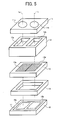
- Fig. 3 is a diagram illustrating an example of the LED arrangement of the light emission unit.
- the light emission unit 20 is structured by arranging multiple infrared LEDs around the image pickup unit 10 to cause the luminance of the image of the driver 1 to be uniform.
- Fig. 3A is a diagram illustrating an example in which multiple LEDs 21 that outputs near infrared in the wavelength range of from approximately 800 to 1,000 nm are uniformly arranged.
- Fig. 3B is a diagram illustrating an example in which infrared LEDs 22 and 23 emit beams of light having a single wavelength of 870 nm and 970 nm, respectively. Since LEDs have directionality, the LEDs 22 and 23 are arranged in a pattern illustrated in Fig.
- a diffusion board is optionally provided on the side of irradiation of the LEDs.
- the group of the infrared LEDs of Fig. 3A that output near infrared in the band of from approximately 800 to 1,000 nm or the group of the infrared LEDs of Fig. 3B that output a single wavelength of 870 nm or 970 nm is driven with a regular interval to irradiate the face portion of the driver 1 in a pulse manner via the near infrared bandpass filter 30 and the image pickup 10 receives the reflection light from the face portion only during this irradiation.
- the image pickup unit 10 separates this reflection light image and transmits the reflection light image through a color filter to obtain two images of two different reflection characteristics of two different wavelengths of 870 nm and 970 nm at the same time.
- Fig. 4 is a diagram illustrating the characteristics of the transmission ratio to the reflection ratio of a near infrared bandpass filter.
- the near infrared bandpass filter 30 are required to transmit only the near infrared projected to the face of the driver 1 by the LEDs and reflect the optical light for the driver 1 and ambient light. Therefore, a filter having the characteristics of the transmission ratio to the reflection ratio as illustrated in Fig. 3 is used.
- Such a filter is easily manufactured by using photonic crystal, a sub-wavelength structure or a laminar structure in which each layer has a different refraction index.
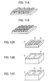
- Fig. 5 is an exploded perspective view illustrating the structure of the image pickup unit in the image pickup of the embodiment illustrated in Fig. 1 .
- Fig. 6 is a cross section illustrating the structure of the image pickup unit in the image pickup of the embodiment illustrated in Fig. 1 .
- the image pickup unit 10 employs a compound eye system in which multiple lenses (two in this case) are used for one image pickup element. This compound eye system has an advantage in that the device is reduced in thickness.
- the two lenses 11a and 11b are independent single lenses having the same form arranged on the same plane and form a lens array 11.
- Each of the optical axes 1a and 1b of the two lenses 11a and 11b is parallel to the normal line of the plane on which the two lenses 11a and 11b are arranged.
- the two single lenses 11a and 11b are formed of, for example, a nonspherical lens, etc.
- the direction in parallel with the optical axes 1a and 1b is defined to be Z axis
- a direction perpendicular to the Z axis is defined to be X axis
- the direction perpendicular to the Z axis and the X axis is defined to be Y axis.
- the lenses 11a and 11b are situated on the lattice points formed of a straight line in parallel with the X axis and a straight line in parallel with the Y axis on the XY plane.
- the light shield spacer 12 is provided on the opposite side of an object relative to the lens array 11.
- the light shield spacer 12 has openings (holes) 12a and 12b with the respective optical axes 1a and 1b as their centers.
- the openings 12a and 12b are empty holes (air layer) and the inside wall of the openings is treated (e.g., black-lacquered, roughened or matted) to prevent reflection of light, therefore, preventing stray light reflected at the inside wall from entering into the solid image pickup element, which is described later.
- a color filter 13 on which color filter areas 13a and 13b are formed is arranged on the opposite side of the object relative to the light shield spacer 12.
- the color filter areas 13a and 13b are respectively provided in a plane parallel to the XY plane where the optical axes 1a and 1b pass.
- the color filter is an element which transmits only light beams having a particular wavelength.
- the color filter area 13a transmits near infrared having a wavelength of 870 nm and the color filter area 13b transmits near infrared having a wavelength of 970 nm.
- An image pickup element holder 15 is provided via a spacer 14 on the opposite side of the object relative to the color filter 13.
- the image pickup holder 15 includes a substrate 17 having a digital signal processor (DSP) on which a solid image pickup element 16 such as a CCD is provided.
- DSP digital signal processor
- the image pickup areas (areas on which the object is actually focused) of the solid image pickup element 16 are located on the same plane parallel to the XY plane.
- the optical axes 1a and 1b approximately pass through the corresponding centers of the two equally divided areas 16a and 16b (enclosed by dashes lines in this embodiment) of the image pickup area.
- the spacer 14 having a rectangle frame form is placed on the image pickup holder 15 and the color filter 13 is provided on the spacer 14.
- the image pickup areas 16a and 16b of the image pickup element 16 are sealed by the spacer 14, the color filter 13 and the image pickup holder 15 to prevent foreign material such as dust from entering into the image pickup areas 16a and 16b.
- the image pickup unit 10 of this embodiment looks like a structure in which two image pickup units independently include a simple lens, a color filter, and an image pickup area on the two optical axes 1a and 1b. Different wavelength images are taken by each image pickup unit, which is described later.
- the near infrared that has passed through the near infrared bandpass filter 30 enters into each of the lenses 11a and 11b of the lens array 11 and then is independently concentrated into particular beams of light.
- Each beam of light after the lenses 11a and 11b is completely separated by the light shield spacer 12 and then enters into each color filter 13a and 13b of the color filter 13.
- the color filter area 13a transmits only near infrared having a wavelength of 970 nm and the color filter area 13b transmits only near infrared having a wavelength of 970 nm.
- the beams of light that have passed through the color filter area 13a of the color filter 13 are received on the area 16a of the solid image pickup element 16 and the beams of light that have passed through the color filter area 13b are received on the area 16b of the solid image pickup element 16. That is, two object images (face images of a driver) having different reflection properties based on the wavelengths of 870 nm and 970 nm are obtained by the solid image pickup element 16 at the same time.
- the lens array 11 is structured by an array of simple lenses.
- a structure illustrated in Fig. 7A is suitable in which multiple lens arrays 111 are accumulated via a spacer 112.
- the form of each lens is made simple by increasing the number of lenses, which resultantly makes manufacturing of each lens easy.
- the form of each lens can be changed as illustrated in Fig. 7B .
- the iris is adjusted by changing the aperture of the lens since the amount of incident light varies depending on the wavelength.
- FIG. 8 A method of manufacturing a lens array is illustrated in Fig. 8 . Refer to P13 to P20 of Ricoh Technical Report, No. 29, published in December 2003.
- the reflow method illustrated in Fig. 8A is as follows: manufacture a photoresist pattern having a pillar form by photolithography on the surface of a glass substrate; heat the glass substrate to flow the photoresist; and form a lens form by the surface tension.
- the ion diffusion method illustrated in Fig. 8B is a method in which gradual changes in the refraction index are made on the glass substrate on which a mask to a lens form is formed by diffusing an ion such as Tl + in the glass substrate.
- the inkjet method illustrated in Fig. 8C is as follows: drop a tiny amount of resin material to a predetermined position using an inkjet printer head; and manufacture a lens form by the surface tension.
- the gray scale mask method is illustrated in Fig. 8D .
- the photoresist form is controlled by the transmission ratio distribution provided to a gray scale mask.
- This method is relatively suitable to form various kinds of forms in comparison with the other methods.
- the gray scale method is increasingly important for the lens manufacturing technology in the future.
- a lens manufactured by a photoresist has problems such that the lens manufactured as is has an insufficient transmission ratio and a weak resistance to humidity or exposure to light. Therefore, the resist pattern is transferred to a substrate material first by using an anisotropic dry etching.
- the resist form prepared by an anisotropic dry etching process may significantly different from the resist form before the etching. Thus, manufacturing a lens with a small error from the target form is difficult.
- this form change varies depending on the kind of used etching devices, the etching condition, and the kind of the material for a substrate.
- the important factors such as the transmission ratio, the wavelength range, and the refraction index in terms of the evaluation on a lens are affected by the kind of the substrate. Therefore, making it possible to manufacture a lens having a high form precision from various kinds of substrate material is preferable.
- a typical method of manufacturing a lens by grinding and a mold method of manufacturing a die and sealing a resin material into the die are also suitably used although these are not illustrated in figures.
- Fig. 9 is a conceptual diagram illustrating a color filter formed of photonic crystal. That is, a transparent medium 132 having a high fraction ratio and a medium 133 having a low fraction ratio are alternately accumulated while preserving the form of the interface therebetween.
- Each layer is of a periodicity in the X direction but can be uniform in the Y direction or have a periodic or non-periodic structure larger than the periodicity in the X direction.
- Such a fine periodic structure of photonic crystal can be manufactured with high reproducibility and uniformity by a system using a technology referred to as the self-cloning technology.
- Fig. 10 is a schematic diagram illustrating the color filter formed of two kinds of areas that transmit beams of light having different wavelengths.
- the color filter 13 has a structure illustrated in Fig. 9 , which is a laminar structure, for example, including multiple alternate layers of Ta 2 O 5 and SiO 2 , having at least two kinds of transparent materials alternately accumulated along the Z direction on one substrate arranged in parallel with the XY plane in the orthogonal coordinate system.
- the color filter 13 is separated into two areas 13a and 13b in the XY plane in this embodiment and each area has a concavo-convex structure periodically repeated in one direction in the XY plane which is determined depending on each area.
- beams of light having two wavelengths ( ⁇ 1 and ⁇ 2: ⁇ 1 ⁇ ⁇ 2) enter vertically into one of the main planes of the photonic crystal filter, signal beams of light having a particular wavelength are selectively output from the other one of the main planes.
- the opening areas and the transmission axes of the color filter described above can be freely designed according to the size and/or direction of the groove patterns processed on a substrate first.
- the groove patterns are formed by various kinds of methods using, for example, electron beam lithography or photolithography, interference exposure, or nano-printing. In any method thereof, the groove direction can be determined for each area with high precision. Therefore, the color filter areas having a combination of fine color filters having different transmission axes, and a color filter having multiple color filter areas can be formed. In addition, only a particular area having a concavo-convex pattern can function as a color filter.
- the color filter 13 is not limited to the photonic crystal type illustrated in Fig. 9 .
- a color filter having a sub-wavelength structure is suitably used.
- the color filter having a sub-wavelength structure has a periodic structure having a shorter cycle than the transmission wavelength. It is known that there is no diffraction wave other than zero dimensional light in a periodic structure having a cycle shorter than the wavelength of light and the optical characteristics of reflection light or transmission light significantly vary depending on the refraction index, thickness, form, etc. of material forming the lattice of the periodic stricture.
- Fig. 11A illustrates an example of the one dimensional sub-wavelength lattice and Fig.
- 11B illustrates a schematic diagram illustrating an example of the two dimensional sub-wavelength lattice.
- the optical characteristics such as reflection characteristics and transmission characteristics change in the one dimensional sub-wavelength lattice depending on the polarization of incident light but the polarization of incident light does not affect the optical characteristics in the two dimensional sub-wavelength lattice.
- Fig. 12 is a diagram illustrating a method of manufacturing a light shield spacer.
- a paint 122 that shields ultraviolet is applied to the outer surface of a sensitive glass 121 containing silver.
- the paint 122 is removed by patterning from a portion 123 where a shield wall is formed.
- silver precipitates and is blackened at the portion directly irradiated with the ultraviolet among the sensitive glass 121 to form a light shield wall 124.
- the light shield 124 is formed inside the sensitive glass 121.
- the sensitive glass 121 is subject to removal treatment such as mechanical processing or etching to form the light shield spacer 12 having the areas 12a and 12b corresponding to the color filter areas 13a and 13b.
- the light shield spacer 12 is easily manufactured.
- the light shield spacer 12 easily prevents leak of light to the adjacent areas. Therefore, the light shield spacer 12 forms an image pickup unit having a compact size in the XY plane in combination with a lens array having multiple lenses arranged on the same plane.
- the image pickup of the present invention is not limited to the structure having a lens array including two lenses with two color filter areas. Any structure having at least two areas for the lens array and the color filter is suitably used.
- Fig. 13 illustrates a structure having 4 areas.
- Fig. 13 is an exploded perspective view illustrating a schematic structure of the image pickup unit in the image pickup of the second embodiment of the present invention.
- the two lenses 11a and 11b are independent simple lenses having the same form and arranged on the same plane to form the lens array 11.
- two lenses 11c and 11d are simple lenses having the same form but different from that of the two lenses 11a and 11b and are formed on the same plane as that for the two lenses 11a and 11b.
- Each axis of the four lenses 11a, 11b, 11c and 11d is parallel to the normal line of the plane on which the four lenses 11a, 11b, 11c and 11d are arranged.
- the lenses 11a and 11b are formed to mainly obtain images of the driver 1 in a car and 11c and 11d are formed to mainly obtain images of a person sitting at the front passenger seat of the car.
- a parallel direction of the optical axes 1a, 1b, 1c and 1d is defined to be Z axis
- a direction perpendicular to the Z axis is defined to be X axis
- the perpendicular direction to the Z axis and X axis is defined to be Y axis.
- the lenses 11a and 11b are situated on the lattice points formed of a straight line in parallel with the X axis and a straight line in parallel with the Y axis on the XY plane.
- the light shield spacer 12 is provided on the opposite side of an object relative to the lens array 11.
- the light shield spacer 12 has openings (holes) 12a, 12b, 12c and 12d with the respective optical axes 1a, 1b, 1c and 1d as their centers.
- the openings 12a, 12b, 12c and 12d are empty holes (air layer) and the inside wall of the openings is treated (e.g., black-lacquered, roughened or matted) to prevent reflection of light, thereby, preventing stray light reflected on the inside wall from entering into the solid image pickup element, which is described later.
- a color filter 13 on which color filter areas 13a, 13b, 13c and 13d are formed is arranged on the opposite side of an object relative to the light shield spacer 12.
- the color filter areas 13a, 13b, 13c and 13d are respectively provided in a plane parallel to the XY plane where the optical axes 1a, 1b, 1c and 1d pass.
- the color filter is an element which transmits only light beams having a particular wavelength.
- the color filter areas 13a and 13b transmit near infrared having a wavelength of 870 nm and the color filter areas 13b and 13d transmit near infrared having a wavelength of 970 nm.
- An image pickup element holder 15 is provided via a spacer 14 on the opposite side of the object relative to the color filter 13.
- the image pickup holder 15 includes a substrate having a digital signal processor (DSP) on which a solid image pickup element 16 such as a CCD is provided.
- DSP digital signal processor
- the image pickup areas (areas on which the object is actually focused) of the solid image pickup element 16 are located on the same plane parallel to the XY plane.
- the optical axes 1a, 1b, 1c and 1d approximately pass through the corresponding centers of the four equally divided areas 16a, 16b, 16c and 16d (enclosed by dashes lines in this embodiment) of the image pickup area.
- Both images of the driver 1 and the front passenger in a car are optimally focused by employing a structure in which a lens array having lenses for the driver 1 and the front passenger is arranged.
- a processing unit having the same form as in the first embodiment is provided at the rear of each image pickup element to take images according to the wavelength information. Therefore, the image pickup having a more robust property to the image shooting position than that of the first embodiment is manufactured.
- the structure in which the image pickup of the present invention is built in a rear view mirror to shoot images of the driver is described above.
- the image pickup of the present invention is not limited thereto.
- the camera may be built in an instrument panel or can be arranged in combination with a head-up display.
- the image pickup of the present invention is not limited to the usage for a car but can be used for a factory (for factory automation) or in a healthcare medical field.
Landscapes
- Engineering & Computer Science (AREA)
- Physics & Mathematics (AREA)
- Chemical & Material Sciences (AREA)
- Life Sciences & Earth Sciences (AREA)
- Optics & Photonics (AREA)
- Health & Medical Sciences (AREA)
- Crystallography & Structural Chemistry (AREA)
- Multimedia (AREA)
- General Physics & Mathematics (AREA)
- Signal Processing (AREA)
- Nanotechnology (AREA)
- Manufacturing & Machinery (AREA)
- Biophysics (AREA)
- Social Psychology (AREA)
- Biomedical Technology (AREA)
- Medical Informatics (AREA)
- Molecular Biology (AREA)
- Surgery (AREA)
- Animal Behavior & Ethology (AREA)
- General Health & Medical Sciences (AREA)
- Public Health (AREA)
- Veterinary Medicine (AREA)
- Heart & Thoracic Surgery (AREA)
- Pathology (AREA)
- Psychology (AREA)
- Psychiatry (AREA)
- Hospice & Palliative Care (AREA)
- Educational Technology (AREA)
- Developmental Disabilities (AREA)
- Child & Adolescent Psychology (AREA)
- Color Television Image Signal Generators (AREA)
- Studio Devices (AREA)
- Blocking Light For Cameras (AREA)
Abstract
Description
- The present invention relates to an image pickup, and more particularly to an image pickup for use in the detection of the driving status of a driver, etc.
- In recent years, detecting and monitoring the driving status of a driver all the time has been studied related to the drive assist system. In general, a method of taking a face image of a driver by an image pickup camera built in a rear view mirror (hereinafter referred to as a rear view mirror built-in image pickup) is used to detect the status of the driver. Securely taking face images of a driver in a wide range of illuminance from day to night is necessary.
- A rear view mirror built-in image pickup adopting a near infrared pulse light projection method is already present to securely take face images of a driver from a low illuminance during night to a high illuminance during daytime. In this rear view mirror built-in image pickup, a light emission unit in which LEDs emitting light having a wavelength of 850 nm are arranged, an image pickup unit of a charge-coupled camera (CCD), etc are built-in a rear view mirror. The rear view mirror built-in image pickup irradiates an object (driver) with beams of near infrared having a wavelength of 850nm in a pulse manner during which the shutter of the CCD camera is open to receive a reflection light image. When taking an image of a driver, a near infrared bandpass filter mirror which transmits beams of near infrared and reflects optical light required for the driver is used to receive a reflection light image with the CCD camera formed by irradiating the driver with the beams of near infrared without a loss while not hindering the function of the rear view mirror. In this rear view mirror built-in image pickup, images of a driver are securely obtained by using near infrared.
- The object of detecting and monitoring the status of a driver during driving is to detect and monitor deterioration of consciousness due to dozing off, inattentive driving, etc. The rear view mirror built-in image pickup described above shoots a face image of a driver, takes out (detects) the face area and eye area from the face image, and measures blinks and the direction of the line of sight. The rear view mirror built-in image pickup detects the degree of deterioration of consciousness from the change in the time of shutting eyes of blinking and inattentive view from the direction of the face and/or the eyeball.
- As described above, taking out the face area and the eye area from the face image of a driver taken by an image pickup is necessary to detect the driving status of the driver. Thus, placing the position of those areas at a high speed with high precision is demanded. For example, precision is required such that when a dummy (mannequin) sits at wheel, the dummy's face is not detected as the face of man. The rear view mirror built-in image pickup can securely shoot face images of a driver in the environment in which the illuminance changes from day to night. However, since the rear view mirror built-in image pickup employs a method of using only near infrared light having a single wavelength of 850 nm, placing the position of the face of a driver is limiting with regard to high precision.
- In addition, another device, i.e., a near infrared multi-band image pickup, exists and uses near infrared light having a wavelength of 870 nm and near infrared having a wavelength of 970 nm. The near infrared multi-band image pickup irradiates the driver with near infrared having a wavelength of 870 nm and near infrared having a wavelength of 970 nm sequentially to obtain two images of 870 nm and 970 nm by a CCD camera. The image pickup detects the skin and hair portions by calculating the difference between the luminance values of the two irradiation images and discriminates the two portions from the symbol of the difference. The optical light is cut by an optical filter so that a secure image can be obtained.
- The near infrared multi-band image pickup makes it possible to place the face of man with high accuracy but since the infrared having a wavelength of 870 nm and the infrared having a wavelength of 970 nm are emitted sequentially, images should be obtained by sequential lighting in a synchronized manner, which causes problems with regard to complexity and real time property.
- Because of these reasons, the present inventor recognizes that a need exists for an image pickup which detects the driving status of a driver by placing the face portion of the driver with high precision and taking a face image in a real time manner.
- Accordingly, an object of the present invention is to provide an image pickup which detects the driving status of a driver by locating the face portion of the driver with high precision and extracting a face image in a real time manner.
- Briefly this object and other objects of the present invention as hereinafter described will become more readily apparent and can be attained, either individually or in combination thereof, by an image pickup including a light emission portion that irradiates an object with near infrared; and an image pickup portion that receives a reflection light image of the object by the near infrared. The image pickup portion includes a lens array containing a substrate on which multiple lenses to respectively receive the reflection light image of the object by the near infrared are arranged; a light shield spacer that shields beams of light that have passed through the lens array from each other; a color filter separated into areas according to beams of light that pass through the light shield spacer, each of which transmits only particular beams of near infrared depending on the wavelengths thereof; and an image pickup element that simultaneously obtains multiple images of the object which are formed of each of the particular beams of near infrared having independent wavelengths that have passed through each of the areas of the color filter.
- It is preferred that, in the image pickup mentioned above, the color filter is a laminate structure in which, in an XYZ orthogonal coordinate system, at least two kinds of transparent materials are alternately arranged in the Z direction on a substrate arranged in parallel with the XY plane, each layer of the laminate structure has one dimensional periodic concavo-convex form repeated in one direction in the XY plane determined depending on each of the areas and the beams of light that pass through the light shield spacer enters into the XY plane.
- It is still further preferred that, in the image pickup mentioned above, the color filter has a groove or lattice structure arranged on a substrate with a regular cycle.
- It is still further preferred that, in the image pickup mentioned above, the image pickup element is installed on an image pickup element holder, a spacer having a rectangle frame is provided on the image pickup element holder, the color filter is installed on the spacer, and the image pickup element is sealed by the spacer, the color filter, and the image pickup element holder.
- These and other objects, features and advantages of the present invention will become apparent upon consideration of the following description of the preferred embodiments of the present invention taken in conjunction with the accompanying drawings.
- Various other objects, features and attendant advantages of the present invention will be more fully appreciated as the same becomes better understood from the detailed description when considered in connection with the accompanying drawings in which like reference characters designate like corresponding parts throughout and wherein:
-
Fig. 1 is a diagram illustrating an example of the entire structure of the image pickup related to a first embodiment of the present invention; -
Fig. 2 is a diagram illustrating the characteristics of reflection characteristics in the near infrared range of the skin and hair of man; -
Fig. 3 is a diagram illustrating an example of the LED arrangement of the light emission portion; -
Fig. 4 is a diagram illustrating the characteristics of the transmission ratio/reflection ratio of a near infrared bandpass filter; -
Fig. 5 is an exploded perspective view of the structure of the image pickup unit in the image pickup of the first embodiment of the present invention; -
Fig. 6 is a cross section illustrating the structure of the image pickup unit of the image pickup of the first embodiment of the present invention; -
Fig. 7 is a diagram illustrating another example of the structure of the lens array for use in the present invention; -
Fig. 8 is a diagram illustrating an example of the method of manufacturing the lens array for use in the present invention; -
Fig. 9 is a diagram illustrating an example of the structure of the color filter for use in the present invention; -
Fig. 10 is a diagram illustrating an example of the color filter of having the structure illustrated inFig. 9 ; -
Fig. 11 is a diagram illustrating another example of the structure of the color filter for use in the present invention; -
Fig. 12 is a diagram illustrating an example of the method of manufacturing the light shield for use in the present invention; and -
Fig. 13 is a diagram illustrating an example of the structure of the image pickup unit of the image pickup related to a second embodiment of the present invention. - The present invention will be described below in detail with reference to several embodiments and accompanying drawings. In the embodiments specified below, infrared having a wavelength of 870 nm and infrared having a wavelength of 970 nm are used in the near infrared multi-band image pickup described above. However, there is no specific limit to the number of the wavelengths. In general, higher precision processing is possible with a greater number of wavelengths.
-
Fig. 1 is a schematic diagram illustrating the entire structure of the image pickup related to a first embodiment of the present invention. InFig. 1 , areference numeral 10 represents an image pickup unit such as a charge coupled device (CCD) that shoots a face image of a driver. 1 as the object, and areference numeral 20 represents a light emission unit that irradiates the driver 1 with near infrared using an infrared LED. Theimage pickup unit 10 and thelight emission unit 20 are built in arear view mirror 50 of a car to obtain the face image of the driver without being affected by the driving operation. A nearinfrared bandpass filter 30 is provided on the front of therear view mirror 50. The nearinfrared bandpass filter 30 transmits emitted near infrared and reflects optical light so that the near infrared is projected to the driver 1 without a loss and the reflection light is received at theimage pickup unit 10 while avoiding hindrance of the function of therear view mirror 50 by taking images of the driver 1. In addition, a controller (not shown) which controls the shutter speed and the gain of the camera in theimage pickup unit 10, and the emission timing of the infrared LED of thelight emission unit 20 is built in therear view mirror 50. - The
light emission unit 20 emits near infrared in a pulse manner in synchronization with the image pickup timing determined by the controller (not shown). This near infrared passes through the nearinfrared bandpass filter 30 and is projected to the face portion of the driver 1. The reflection light passes through the nearinfrared bandpass filter 30 and is received on theimage pickup unit 10 such as a CCD camera. - The
image pickup unit 10 separates the received near infrared into two beams of light via a lens array employing a compound eye system and each beam of light enters into a color filter separated into different areas depending on the transmission wavelength of 870 nm or 970 nm and then into the image pickup element such as a CCD. Thus, two object (driver) images having different reflective characteristics reflecting the two wavelengths of 870 nm and 970 nm are obtained at the same time. A specific structure example of theimage pickup 10 is described later. - Although invisible to a human being, a CCD camera can generally sense light beams having a wavelength of from 770 to 1,000 nm in the near infrared range. The reflection characteristics of the face portion of a man in the near infrared range are known as illustrated in
Fig. 2 . As in the case of the near infrared multi-band image pickup described above in the discussion of the background, when comparing the luminance values of the obtained two object images shot by using the selected two beams of light having wavelengths of 870 nm and 970 nm, the reflection characteristics of the skin and the hair are opposite, i.e., diagonally right down and right up, respectively. Therefore, when calculating the difference between the two object images, the symbols of the difference are opposite depending on the skin or the hair. Thus, the skin and the hair are discernable by the difference of the two object images shot by light beams having a wavelength of 870 nm and 970 nm. - After placing the skin portion, as in the case of the rear view mirror built-in image pickup described above in the discussion of the background, the face area and the eye area are detected followed by measuring blinking and the direction of the line of sight. The rear view mirror built-in image pickup detects the degree of deterioration of consciousness from the change in the time of shutting eyes due to blinking and inattentive view from the direction of the face and/or the eyeball. The rear view mirror built-in image pickup issues a caution to the driver 1 based on the obtained information.
- The image pickup of this embodiment is improved in comparison with the near infrared multi-band image pickup described above in regards to the real time property because the two images having different reflection properties based on the two different wavelengths of 870 nm and 970 nm in the near infrared range are obtained at the same time. In addition, the image pickup of this embodiment is improved in comparison with the rear view mirror built-in image pickup described above in regards to the accuracy on placement of the face position of the driver 1 because the skin and hair portions are cut by calculating the difference between the luminance values of the two obtained image. Since the embodiment employs a near infrared pulse light projection method, the image pickup of the embodiment securely obtains an image in the environment from a low illuminance during night to a high illuminance during daytime as in the case of the rear view mirror built-in image pickup described above. Furthermore, since the image pickup of the embodiment is built in the
rear view mirror 50 of a car, the face of the driver 1 is taken without being affected by the driving operation. - Structure examples of each unit of the image pickup of the present invention are described below with descriptions about the function, etc.
-
Fig. 3 is a diagram illustrating an example of the LED arrangement of the light emission unit. In the example illustrated inFig. 3 , thelight emission unit 20 is structured by arranging multiple infrared LEDs around theimage pickup unit 10 to cause the luminance of the image of the driver 1 to be uniform.Fig. 3A is a diagram illustrating an example in whichmultiple LEDs 21 that outputs near infrared in the wavelength range of from approximately 800 to 1,000 nm are uniformly arranged.Fig. 3B is a diagram illustrating an example in whichinfrared LEDs LEDs Fig. 3B to cancel un-uniformity of light. A diffusion board is optionally provided on the side of irradiation of the LEDs. The group of the infrared LEDs ofFig. 3A that output near infrared in the band of from approximately 800 to 1,000 nm or the group of the infrared LEDs ofFig. 3B that output a single wavelength of 870 nm or 970 nm is driven with a regular interval to irradiate the face portion of the driver 1 in a pulse manner via the nearinfrared bandpass filter 30 and theimage pickup 10 receives the reflection light from the face portion only during this irradiation. As described later, theimage pickup unit 10 separates this reflection light image and transmits the reflection light image through a color filter to obtain two images of two different reflection characteristics of two different wavelengths of 870 nm and 970 nm at the same time. -
Fig. 4 is a diagram illustrating the characteristics of the transmission ratio to the reflection ratio of a near infrared bandpass filter. The nearinfrared bandpass filter 30 are required to transmit only the near infrared projected to the face of the driver 1 by the LEDs and reflect the optical light for the driver 1 and ambient light. Therefore, a filter having the characteristics of the transmission ratio to the reflection ratio as illustrated inFig. 3 is used. Such a filter is easily manufactured by using photonic crystal, a sub-wavelength structure or a laminar structure in which each layer has a different refraction index. -
Fig. 5 is an exploded perspective view illustrating the structure of the image pickup unit in the image pickup of the embodiment illustrated inFig. 1 .Fig. 6 is a cross section illustrating the structure of the image pickup unit in the image pickup of the embodiment illustrated inFig. 1 . Theimage pickup unit 10 employs a compound eye system in which multiple lenses (two in this case) are used for one image pickup element. This compound eye system has an advantage in that the device is reduced in thickness. - In
Fig. 5 , the twolenses lens array 11. Each of theoptical axes lenses lenses single lenses - As illustrated in
Fig. 5 , the direction in parallel with theoptical axes lenses - The
light shield spacer 12 is provided on the opposite side of an object relative to thelens array 11. Thelight shield spacer 12 has openings (holes) 12a and 12b with the respectiveoptical axes openings - A
color filter 13 on whichcolor filter areas light shield spacer 12. Thecolor filter areas optical axes color filter area 13a transmits near infrared having a wavelength of 870 nm and thecolor filter area 13b transmits near infrared having a wavelength of 970 nm. - An image
pickup element holder 15 is provided via aspacer 14 on the opposite side of the object relative to thecolor filter 13. Theimage pickup holder 15 includes asubstrate 17 having a digital signal processor (DSP) on which a solidimage pickup element 16 such as a CCD is provided. The image pickup areas (areas on which the object is actually focused) of the solidimage pickup element 16 are located on the same plane parallel to the XY plane. Theoptical axes areas - As illustrated in
Fig. 6 , thespacer 14 having a rectangle frame form is placed on theimage pickup holder 15 and thecolor filter 13 is provided on thespacer 14. Theimage pickup areas image pickup element 16 are sealed by thespacer 14, thecolor filter 13 and theimage pickup holder 15 to prevent foreign material such as dust from entering into theimage pickup areas - As described above, the
image pickup unit 10 of this embodiment looks like a structure in which two image pickup units independently include a simple lens, a color filter, and an image pickup area on the twooptical axes - As illustrated in
Fig. 1 , the near infrared that has passed through the nearinfrared bandpass filter 30 enters into each of thelenses lens array 11 and then is independently concentrated into particular beams of light. Each beam of light after thelenses light shield spacer 12 and then enters into eachcolor filter color filter 13. Thecolor filter area 13a transmits only near infrared having a wavelength of 970 nm and thecolor filter area 13b transmits only near infrared having a wavelength of 970 nm. The beams of light that have passed through thecolor filter area 13a of thecolor filter 13 are received on thearea 16a of the solidimage pickup element 16 and the beams of light that have passed through thecolor filter area 13b are received on thearea 16b of the solidimage pickup element 16. That is, two object images (face images of a driver) having different reflection properties based on the wavelengths of 870 nm and 970 nm are obtained by the solidimage pickup element 16 at the same time. - In
Figs. 5 and6 , thelens array 11 is structured by an array of simple lenses. Also, a structure illustrated inFig. 7A is suitable in whichmultiple lens arrays 111 are accumulated via aspacer 112. The form of each lens is made simple by increasing the number of lenses, which resultantly makes manufacturing of each lens easy. In addition, the form of each lens can be changed as illustrated inFig. 7B . For example, the iris is adjusted by changing the aperture of the lens since the amount of incident light varies depending on the wavelength. - A method of manufacturing a lens array is illustrated in
Fig. 8 . Refer to P13 to P20 of Ricoh Technical Report, No. 29, published in December 2003. - The reflow method illustrated in
Fig. 8A is as follows: manufacture a photoresist pattern having a pillar form by photolithography on the surface of a glass substrate; heat the glass substrate to flow the photoresist; and form a lens form by the surface tension. The ion diffusion method illustrated inFig. 8B is a method in which gradual changes in the refraction index are made on the glass substrate on which a mask to a lens form is formed by diffusing an ion such as Tl+ in the glass substrate. The inkjet method illustrated inFig. 8C is as follows: drop a tiny amount of resin material to a predetermined position using an inkjet printer head; and manufacture a lens form by the surface tension. - These methods use forms or refraction index distribution naturally created by the surface tension or ion diffusion as a lens. The gray scale mask method is illustrated in
Fig. 8D . In this method, the photoresist form is controlled by the transmission ratio distribution provided to a gray scale mask. This method is relatively suitable to form various kinds of forms in comparison with the other methods. Thus, the gray scale method is increasingly important for the lens manufacturing technology in the future. - The reflow method and the gray scale method illustrated in
Fig. 8 are illustrated until the lens form is formed by the photoresist. Generally, a lens manufactured by a photoresist has problems such that the lens manufactured as is has an insufficient transmission ratio and a weak resistance to humidity or exposure to light. Therefore, the resist pattern is transferred to a substrate material first by using an anisotropic dry etching. However, the resist form prepared by an anisotropic dry etching process may significantly different from the resist form before the etching. Thus, manufacturing a lens with a small error from the target form is difficult. In addition, this form change varies depending on the kind of used etching devices, the etching condition, and the kind of the material for a substrate. Particularly, the important factors such as the transmission ratio, the wavelength range, and the refraction index in terms of the evaluation on a lens are affected by the kind of the substrate. Therefore, making it possible to manufacture a lens having a high form precision from various kinds of substrate material is preferable. - In addition, a typical method of manufacturing a lens by grinding and a mold method of manufacturing a die and sealing a resin material into the die are also suitably used although these are not illustrated in figures.
- Next, the color filter is described.
Fig. 9 is a conceptual diagram illustrating a color filter formed of photonic crystal. That is, atransparent medium 132 having a high fraction ratio and a medium 133 having a low fraction ratio are alternately accumulated while preserving the form of the interface therebetween. Each layer is of a periodicity in the X direction but can be uniform in the Y direction or have a periodic or non-periodic structure larger than the periodicity in the X direction. Such a fine periodic structure of photonic crystal can be manufactured with high reproducibility and uniformity by a system using a technology referred to as the self-cloning technology. -
Fig. 10 is a schematic diagram illustrating the color filter formed of two kinds of areas that transmit beams of light having different wavelengths. Thecolor filter 13 has a structure illustrated inFig. 9 , which is a laminar structure, for example, including multiple alternate layers of Ta2O5 and SiO2, having at least two kinds of transparent materials alternately accumulated along the Z direction on one substrate arranged in parallel with the XY plane in the orthogonal coordinate system. Thecolor filter 13 is separated into twoareas - When beams of light having two wavelengths (λ1 and λ2: λ1 < λ2) enter vertically into one of the main planes of the photonic crystal filter, signal beams of light having a particular wavelength are selectively output from the other one of the main planes.
- The opening areas and the transmission axes of the color filter described above can be freely designed according to the size and/or direction of the groove patterns processed on a substrate first. The groove patterns are formed by various kinds of methods using, for example, electron beam lithography or photolithography, interference exposure, or nano-printing. In any method thereof, the groove direction can be determined for each area with high precision. Therefore, the color filter areas having a combination of fine color filters having different transmission axes, and a color filter having multiple color filter areas can be formed. In addition, only a particular area having a concavo-convex pattern can function as a color filter. Therefore, when the areas around the particular area are made to have a flat pattern or a concavo-convex pattern isotropic in the plane, light passes through the areas as media not having polarized wave dependency. Therefore, a color filter can be formed only on the particular area.
- The
color filter 13 is not limited to the photonic crystal type illustrated inFig. 9 . For example, a color filter having a sub-wavelength structure is suitably used. The color filter having a sub-wavelength structure has a periodic structure having a shorter cycle than the transmission wavelength. It is known that there is no diffraction wave other than zero dimensional light in a periodic structure having a cycle shorter than the wavelength of light and the optical characteristics of reflection light or transmission light significantly vary depending on the refraction index, thickness, form, etc. of material forming the lattice of the periodic stricture.Fig. 11A illustrates an example of the one dimensional sub-wavelength lattice andFig. 11B illustrates a schematic diagram illustrating an example of the two dimensional sub-wavelength lattice. The optical characteristics such as reflection characteristics and transmission characteristics change in the one dimensional sub-wavelength lattice depending on the polarization of incident light but the polarization of incident light does not affect the optical characteristics in the two dimensional sub-wavelength lattice. - Next, the light shield spacer is described.
Fig. 12 is a diagram illustrating a method of manufacturing a light shield spacer. As illustrated inFig. 12A , apaint 122 that shields ultraviolet is applied to the outer surface of asensitive glass 121 containing silver. Thepaint 122 is removed by patterning from aportion 123 where a shield wall is formed. After thesensitive glass 121 is irradiated with ultraviolet and thepaint 122 is removed, silver precipitates and is blackened at the portion directly irradiated with the ultraviolet among thesensitive glass 121 to form alight shield wall 124. Thelight shield 124 is formed inside thesensitive glass 121. Finally, as illustrated inFig. 12C , thesensitive glass 121 is subject to removal treatment such as mechanical processing or etching to form thelight shield spacer 12 having theareas color filter areas - According to the method illustrated in
Fig. 12 , thelight shield spacer 12 is easily manufactured. In addition, thelight shield spacer 12 easily prevents leak of light to the adjacent areas. Therefore, thelight shield spacer 12 forms an image pickup unit having a compact size in the XY plane in combination with a lens array having multiple lenses arranged on the same plane. - The image pickup of the present invention is not limited to the structure having a lens array including two lenses with two color filter areas. Any structure having at least two areas for the lens array and the color filter is suitably used. For example,
Fig. 13 illustrates a structure having 4 areas. -
Fig. 13 is an exploded perspective view illustrating a schematic structure of the image pickup unit in the image pickup of the second embodiment of the present invention. InFig. 13 , the twolenses lens array 11. In addition, twolenses lenses lenses lenses lenses lenses - As illustrated in
Fig. 13 , a parallel direction of theoptical axes lenses - The
light shield spacer 12 is provided on the opposite side of an object relative to thelens array 11. Thelight shield spacer 12 has openings (holes) 12a, 12b, 12c and 12d with the respectiveoptical axes openings - A
color filter 13 on whichcolor filter areas light shield spacer 12. Thecolor filter areas optical axes color filter areas color filter areas - An image
pickup element holder 15 is provided via aspacer 14 on the opposite side of the object relative to thecolor filter 13. Theimage pickup holder 15 includes a substrate having a digital signal processor (DSP) on which a solidimage pickup element 16 such as a CCD is provided. The image pickup areas (areas on which the object is actually focused) of the solidimage pickup element 16 are located on the same plane parallel to the XY plane. Theoptical axes areas - As an example of the image pickup of the present invention, the structure in which the image pickup of the present invention is built in a rear view mirror to shoot images of the driver is described above. The image pickup of the present invention is not limited thereto. The camera may be built in an instrument panel or can be arranged in combination with a head-up display. Furthermore, the image pickup of the present invention is not limited to the usage for a car but can be used for a factory (for factory automation) or in a healthcare medical field.
- This document claims priority and contains subject matter related to Japanese Patent Applications Nos.
2008-159051 2009-013235
Claims (5)
- An image pickup comprising:a light emission portion configured to irradiate an object with near infrared; andan image pickup portion configured to receive a reflection light image of the object by the near infrared, the image pickup portion comprising:a lens array comprising a substrate on which multiple lenses to respectively receive the reflection light image of the object by the near infrared are arranged;a light shield spacer configured to shield beams of light that have passed through the lens array from each other;a color filter separated into areas according to beams of light that pass through the light shield spacer, each of the areas being configured to transmit only particular beams of near infrared depending on wavelengths thereof; andan image pickup element configured to simultaneously obtain multiple images of the object which are formed of each of the particular beams of near infrared having independent wavelengths that have passed through each of the areas of the color filter.
- The image pickup according to Claim 1, wherein the color filter is a laminate structure in which, in an XYZ orthogonal coordinate system, at least two kinds of transparent materials are alternately arranged in the Z direction on a substrate arranged in parallel with the XY plane, each layer of the laminate structure has one dimensional periodic concavo-convex form repeated in one direction in the XY plane determined depending on each of the areas and the beams of light that pass through the light shield spacer enters into the XY plane.
- The image pickup according to Claim 1, wherein the color filter has a groove or lattice structure arranged on a substrate with a regular cycle.
- The image pickup according to Claim 1, wherein the image pickup element is installed on an image pickup element holder, a spacer having a rectangle frame is provided on the image pickup element holder, the color filter is installed on the spacer, and the image pickup element is sealed by the spacer, the color filter, and the image pickup element holder.
- A vehicle having an image pickup according to any one of the preceding claims installed therein.
Applications Claiming Priority (2)
| Application Number | Priority Date | Filing Date | Title |
|---|---|---|---|
| JP2008159051 | 2008-06-18 | ||
| JP2009013235A JP5505761B2 (en) | 2008-06-18 | 2009-01-23 | Imaging device |
Publications (2)
| Publication Number | Publication Date |
|---|---|
| EP2136550A2 true EP2136550A2 (en) | 2009-12-23 |
| EP2136550A3 EP2136550A3 (en) | 2011-08-17 |
Family
ID=41137448
Family Applications (1)
| Application Number | Title | Priority Date | Filing Date |
|---|---|---|---|
| EP09251563A Ceased EP2136550A3 (en) | 2008-06-18 | 2009-06-16 | Image pickup |
Country Status (4)
| Country | Link |
|---|---|
| US (1) | US8379084B2 (en) |
| EP (1) | EP2136550A3 (en) |
| JP (1) | JP5505761B2 (en) |
| TW (1) | TWI480189B (en) |
Cited By (14)
| Publication number | Priority date | Publication date | Assignee | Title |
|---|---|---|---|---|
| CN102223482A (en) * | 2011-06-17 | 2011-10-19 | 中国科学院半导体研究所 | Jitter elimination method for moving target gating detection imaging based on CCD external trigger |
| US8242476B2 (en) | 2005-12-19 | 2012-08-14 | Leddartech Inc. | LED object detection system and method combining complete reflection traces from individual narrow field-of-view channels |
| US8310655B2 (en) | 2007-12-21 | 2012-11-13 | Leddartech Inc. | Detection and ranging methods and systems |
| US8436748B2 (en) | 2007-06-18 | 2013-05-07 | Leddartech Inc. | Lighting system with traffic management capabilities |
| US8600656B2 (en) | 2007-06-18 | 2013-12-03 | Leddartech Inc. | Lighting system with driver assistance capabilities |
| US8723689B2 (en) | 2007-12-21 | 2014-05-13 | Leddartech Inc. | Parking management system and method using lighting system |
| US8842182B2 (en) | 2009-12-22 | 2014-09-23 | Leddartech Inc. | Active 3D monitoring system for traffic detection |
| US8908159B2 (en) | 2011-05-11 | 2014-12-09 | Leddartech Inc. | Multiple-field-of-view scannerless optical rangefinder in high ambient background light |
| US9235988B2 (en) | 2012-03-02 | 2016-01-12 | Leddartech Inc. | System and method for multipurpose traffic detection and characterization |
| US9378640B2 (en) | 2011-06-17 | 2016-06-28 | Leddartech Inc. | System and method for traffic side detection and characterization |
| US10297649B2 (en) | 2013-09-19 | 2019-05-21 | Semiconductor Energy Laboratory Co., Ltd. | Light-emitting device, information processing device, and imaging device |
| US10488492B2 (en) | 2014-09-09 | 2019-11-26 | Leddarttech Inc. | Discretization of detection zone |
| CN112188867A (en) * | 2018-12-20 | 2021-01-05 | 松下知识产权经营株式会社 | Biological measurement device, biological measurement method, computer-readable recording medium, and program |
| US11179035B2 (en) | 2018-07-25 | 2021-11-23 | Natus Medical Incorporated | Real-time removal of IR LED reflections from an image |
Families Citing this family (17)
| Publication number | Priority date | Publication date | Assignee | Title |
|---|---|---|---|---|
| JP5590931B2 (en) * | 2010-03-17 | 2014-09-17 | 三菱電機株式会社 | Illuminated surveillance camera device |
| JP5506517B2 (en) * | 2010-04-12 | 2014-05-28 | キヤノン株式会社 | Solid-state image sensor |
| JP2012042229A (en) * | 2010-08-13 | 2012-03-01 | Sony Corp | Detection device, detection method, and electronic apparatus |
| US8594374B1 (en) * | 2011-03-30 | 2013-11-26 | Amazon Technologies, Inc. | Secure device unlock with gaze calibration |
| WO2013021659A1 (en) | 2011-08-11 | 2013-02-14 | 日立マクセル株式会社 | Infrared lens unit, image capture module, and image capture device |
| TWI535555B (en) * | 2011-09-13 | 2016-06-01 | 鴻海精密工業股份有限公司 | Method for manufacturing lens |
| EP3035099B1 (en) | 2013-08-14 | 2020-01-22 | Hitachi Automotive Systems, Ltd. | Imaging module, stereo camera for vehicle, and light shielding member for imaging module |
| JP6536877B2 (en) | 2014-07-31 | 2019-07-03 | パナソニックIpマネジメント株式会社 | Imaging device and imaging system |
| DE102014217750A1 (en) * | 2014-09-04 | 2016-03-10 | Conti Temic Microelectronic Gmbh | Camera system and method for detecting the surroundings of a vehicle |
| WO2016051694A1 (en) * | 2014-09-29 | 2016-04-07 | パナソニックIpマネジメント株式会社 | Hair region detection device and hair region detection method |
| KR20180018550A (en) * | 2015-06-15 | 2018-02-21 | 어그로잉 리미티드 | Multispectral imaging device |
| CN105223756B (en) * | 2015-10-06 | 2018-03-09 | 瑞声光电科技(常州)有限公司 | Array camera lens module |
| EP3373037B1 (en) * | 2017-03-10 | 2023-06-28 | The Hi-Tech Robotic Systemz Ltd | Single casing advanced driver assistance system |
| EP3430798B1 (en) | 2017-03-13 | 2019-06-19 | Lumileds Holding B.V. | Imaging device with an improved autofocusing performance |
| WO2020115682A1 (en) * | 2018-12-05 | 2020-06-11 | Gentex Corporation | Imaging system for iris authentication and driver monitoring |
| JP6884347B2 (en) * | 2019-09-24 | 2021-06-09 | 株式会社ユピテル | Light irradiation system |
| GB2609914A (en) * | 2021-08-12 | 2023-02-22 | Continental Automotive Gmbh | A monitoring system and method for identifying objects |
Citations (6)
| Publication number | Priority date | Publication date | Assignee | Title |
|---|---|---|---|---|
| JP2004228662A (en) * | 2003-01-20 | 2004-08-12 | Minolta Co Ltd | Imaging device |
| JP2006242909A (en) * | 2005-03-07 | 2006-09-14 | Toyota Central Res & Dev Lab Inc | Device part identification device |
| JP2006246193A (en) * | 2005-03-04 | 2006-09-14 | Matsushita Electric Ind Co Ltd | Imaging device |
| WO2007029714A1 (en) * | 2005-09-06 | 2007-03-15 | Tohoku Techno Arch Co., Ltd. | Wavelength division image measuring device |
| JP2008159051A (en) | 2006-12-22 | 2008-07-10 | Palo Alto Research Center Inc | Method for image decimation |
| JP2009013235A (en) | 2007-07-02 | 2009-01-22 | Kyushu Univ | Method for producing alicyclic polymer |
Family Cites Families (40)
| Publication number | Priority date | Publication date | Assignee | Title |
|---|---|---|---|---|
| US6151065A (en) * | 1995-06-20 | 2000-11-21 | Steed; Van P. | Concealed integrated vehicular camera safety system |
| US5555464A (en) * | 1995-07-28 | 1996-09-10 | Lockheed Martin Corporation | Red/near-infrared filtering for CCD cameras |
| JP3325825B2 (en) | 1997-03-29 | 2002-09-17 | 彰二郎 川上 | Three-dimensional periodic structure, method for producing the same, and method for producing film |
| US6213625B1 (en) * | 1999-04-23 | 2001-04-10 | Nsi Enterprises, Inc. | Inverted apex prismatic lens |
| JP3965848B2 (en) * | 1999-12-02 | 2007-08-29 | 富士ゼロックス株式会社 | Optical element, laser array, and method of manufacturing optical element |
| DE10003643A1 (en) * | 2000-01-28 | 2001-08-02 | Reitter & Schefenacker Gmbh | Surveillance device for automobile uses camera behind mirror glass which reflects light in visible wavelength spectrum |
| US6420728B1 (en) * | 2000-03-23 | 2002-07-16 | Manijeh Razeghi | Multi-spectral quantum well infrared photodetectors |
| JP4815677B2 (en) * | 2001-02-20 | 2011-11-16 | ソニー株式会社 | Automotive video camera system and automotive outside mirror |
| JP2003169341A (en) * | 2001-09-19 | 2003-06-13 | Fuji Film Microdevices Co Ltd | Color imaging device |
| JP2003143459A (en) * | 2001-11-02 | 2003-05-16 | Canon Inc | Compound eye imaging system and apparatus equipped with the same |
| JP4088100B2 (en) * | 2002-05-14 | 2008-05-21 | 株式会社村上開明堂 | Rearview mirror with built-in camera |
| US20070052805A1 (en) * | 2002-10-17 | 2007-03-08 | Kabushiki Kaisha Tokai-Rika-Denki-Seisakusho | Interior mirror |
| JP2004191893A (en) | 2002-12-13 | 2004-07-08 | Canon Inc | Imaging apparatus |
| US20060055800A1 (en) * | 2002-12-18 | 2006-03-16 | Noble Device Technologies Corp. | Adaptive solid state image sensor |
| US7221363B2 (en) * | 2003-02-12 | 2007-05-22 | Gentex Corporation | Vehicle information displays |
| US20040256561A1 (en) * | 2003-06-17 | 2004-12-23 | Allyson Beuhler | Wide band light sensing pixel array |
| WO2005041562A1 (en) * | 2003-10-22 | 2005-05-06 | Matsushita Electric Industrial Co., Ltd. | Imaging device and method of producing the device, portable apparatus, and imaging element and method of producing the element |
| JP2005190400A (en) * | 2003-12-26 | 2005-07-14 | Seiko Epson Corp | Face image detection method, face image detection system, and face image detection program |
| CN1568895A (en) | 2004-04-06 | 2005-01-26 | 武汉一海数字工程有限公司 | Breast tissue blood oxygen detection method |
| JP2005303694A (en) * | 2004-04-13 | 2005-10-27 | Konica Minolta Holdings Inc | Compound eye imaging device |
| KR100612014B1 (en) * | 2004-06-29 | 2006-08-11 | 삼성전자주식회사 | Optical pickup and lens assembly device and method |
| JP2006047067A (en) * | 2004-08-03 | 2006-02-16 | Funai Electric Co Ltd | Human body detecting device and human body detecting method |
| JP2006071741A (en) | 2004-08-31 | 2006-03-16 | Olympus Corp | Focus detection device |
| US7145124B2 (en) * | 2004-09-15 | 2006-12-05 | Raytheon Company | Multispectral imaging chip using photonic crystals |
| KR20070057934A (en) * | 2004-09-17 | 2007-06-07 | 마츠시타 덴끼 산교 가부시키가이샤 | Image input device that solves color difference |
| KR100682898B1 (en) * | 2004-11-09 | 2007-02-15 | 삼성전자주식회사 | Imaging device using infrared and its image identification method |
| US7469060B2 (en) * | 2004-11-12 | 2008-12-23 | Honeywell International Inc. | Infrared face detection and recognition system |
| WO2006073085A1 (en) * | 2005-01-04 | 2006-07-13 | I Square Reserch Co., Ltd. | Solid-state image pickup device and method for manufacturing same |
| CN1680779A (en) | 2005-02-04 | 2005-10-12 | 江苏大学 | Driver fatigue monitoring method and device |
| JP2007004155A (en) | 2005-05-27 | 2007-01-11 | Fujifilm Holdings Corp | Antireflection film and method for manufacturing the same |
| JP5023324B2 (en) | 2005-06-27 | 2012-09-12 | 国立大学法人東北大学 | Color filter device and manufacturing method thereof |
| JP4984634B2 (en) * | 2005-07-21 | 2012-07-25 | ソニー株式会社 | Physical information acquisition method and physical information acquisition device |
| JP4807986B2 (en) | 2005-09-05 | 2011-11-02 | 株式会社リコー | Image input device |
| US7423821B2 (en) * | 2006-03-24 | 2008-09-09 | Gentex Corporation | Vision system |
| CN1830389A (en) | 2006-04-21 | 2006-09-13 | 太原理工大学 | Fatigue driving state monitoring device and method |
| JP5106870B2 (en) * | 2006-06-14 | 2012-12-26 | 株式会社東芝 | Solid-state image sensor |
| JP2008005383A (en) * | 2006-06-26 | 2008-01-10 | Matsushita Electric Ind Co Ltd | Imaging device and image sensor |
| KR100827242B1 (en) * | 2006-06-26 | 2008-05-07 | 삼성전기주식회사 | Method and apparatus for image processing |
| JP2008164367A (en) * | 2006-12-27 | 2008-07-17 | Matsushita Electric Ind Co Ltd | Solid-state imaging device, camera, vehicle, and monitoring device |
| JP2008306379A (en) * | 2007-06-06 | 2008-12-18 | Toshiba Corp | Solid-state image sensor |
-
2009
- 2009-01-23 JP JP2009013235A patent/JP5505761B2/en not_active Expired - Fee Related
- 2009-06-16 EP EP09251563A patent/EP2136550A3/en not_active Ceased
- 2009-06-17 US US12/486,246 patent/US8379084B2/en not_active Expired - Fee Related
- 2009-06-17 TW TW098120253A patent/TWI480189B/en not_active IP Right Cessation
Patent Citations (7)
| Publication number | Priority date | Publication date | Assignee | Title |
|---|---|---|---|---|
| JP2004228662A (en) * | 2003-01-20 | 2004-08-12 | Minolta Co Ltd | Imaging device |
| JP2006246193A (en) * | 2005-03-04 | 2006-09-14 | Matsushita Electric Ind Co Ltd | Imaging device |
| JP2006242909A (en) * | 2005-03-07 | 2006-09-14 | Toyota Central Res & Dev Lab Inc | Device part identification device |
| WO2007029714A1 (en) * | 2005-09-06 | 2007-03-15 | Tohoku Techno Arch Co., Ltd. | Wavelength division image measuring device |
| US20090116029A1 (en) * | 2005-09-06 | 2009-05-07 | Yasuo Ohtera | Wavelength division image measuring device |
| JP2008159051A (en) | 2006-12-22 | 2008-07-10 | Palo Alto Research Center Inc | Method for image decimation |
| JP2009013235A (en) | 2007-07-02 | 2009-01-22 | Kyushu Univ | Method for producing alicyclic polymer |
Cited By (21)
| Publication number | Priority date | Publication date | Assignee | Title |
|---|---|---|---|---|
| US8242476B2 (en) | 2005-12-19 | 2012-08-14 | Leddartech Inc. | LED object detection system and method combining complete reflection traces from individual narrow field-of-view channels |
| US8436748B2 (en) | 2007-06-18 | 2013-05-07 | Leddartech Inc. | Lighting system with traffic management capabilities |
| US8600656B2 (en) | 2007-06-18 | 2013-12-03 | Leddartech Inc. | Lighting system with driver assistance capabilities |
| USRE49342E1 (en) | 2007-12-21 | 2022-12-20 | Leddartech Inc. | Distance detection method and system |
| US8310655B2 (en) | 2007-12-21 | 2012-11-13 | Leddartech Inc. | Detection and ranging methods and systems |
| USRE49950E1 (en) | 2007-12-21 | 2024-04-30 | Leddartech Inc. | Distance detection method and system |
| US8723689B2 (en) | 2007-12-21 | 2014-05-13 | Leddartech Inc. | Parking management system and method using lighting system |
| US8842182B2 (en) | 2009-12-22 | 2014-09-23 | Leddartech Inc. | Active 3D monitoring system for traffic detection |
| USRE48763E1 (en) | 2011-05-11 | 2021-10-05 | Leddartech Inc. | Multiple-field-of-view scannerless optical rangefinder in high ambient background light |
| USRE47134E1 (en) | 2011-05-11 | 2018-11-20 | Leddartech Inc. | Multiple-field-of-view scannerless optical rangefinder in high ambient background light |
| US8908159B2 (en) | 2011-05-11 | 2014-12-09 | Leddartech Inc. | Multiple-field-of-view scannerless optical rangefinder in high ambient background light |
| US9378640B2 (en) | 2011-06-17 | 2016-06-28 | Leddartech Inc. | System and method for traffic side detection and characterization |
| CN102223482A (en) * | 2011-06-17 | 2011-10-19 | 中国科学院半导体研究所 | Jitter elimination method for moving target gating detection imaging based on CCD external trigger |
| CN102223482B (en) * | 2011-06-17 | 2013-04-17 | 中国科学院半导体研究所 | Jitter elimination method for moving target gating detection imaging based on CCD external trigger |
| US9235988B2 (en) | 2012-03-02 | 2016-01-12 | Leddartech Inc. | System and method for multipurpose traffic detection and characterization |
| USRE48914E1 (en) | 2012-03-02 | 2022-02-01 | Leddartech Inc. | System and method for multipurpose traffic detection and characterization |
| USRE50261E1 (en) | 2012-03-02 | 2025-01-07 | Leddartech Inc. | System and method for multipurpose traffic detection and characterization |
| US10297649B2 (en) | 2013-09-19 | 2019-05-21 | Semiconductor Energy Laboratory Co., Ltd. | Light-emitting device, information processing device, and imaging device |
| US10488492B2 (en) | 2014-09-09 | 2019-11-26 | Leddarttech Inc. | Discretization of detection zone |
| US11179035B2 (en) | 2018-07-25 | 2021-11-23 | Natus Medical Incorporated | Real-time removal of IR LED reflections from an image |
| CN112188867A (en) * | 2018-12-20 | 2021-01-05 | 松下知识产权经营株式会社 | Biological measurement device, biological measurement method, computer-readable recording medium, and program |
Also Published As
| Publication number | Publication date |
|---|---|
| TW201010887A (en) | 2010-03-16 |
| US8379084B2 (en) | 2013-02-19 |
| TWI480189B (en) | 2015-04-11 |
| US20090316025A1 (en) | 2009-12-24 |
| EP2136550A3 (en) | 2011-08-17 |
| JP5505761B2 (en) | 2014-05-28 |
| JP2010026490A (en) | 2010-02-04 |
Similar Documents
| Publication | Publication Date | Title |
|---|---|---|
| US8379084B2 (en) | Image pickup | |
| EP2136198B1 (en) | Image pickup and method of detecting road status. | |
| JP5145710B2 (en) | Head-up display device | |
| JP5152655B2 (en) | Imaging device | |
| JP4895324B2 (en) | Head-up display device | |
| WO2015015717A1 (en) | Imaging device and imaging system, electronic mirroring system, and distance measurement device using same | |
| JP6230911B2 (en) | Light projector and vision system for distance measurement | |
| TW200912385A (en) | Optical characteristic measuring apparatus using light reflected from object to be measured and focus adjusting method therefor | |
| WO2011114571A1 (en) | Object detecting apparatus and information acquiring apparatus | |
| CN113366262A (en) | Functionalized waveguide for detector system | |
| US7542669B2 (en) | Diffraction display device and viewfinder display device | |
| CN117452747B (en) | 3D structured light system | |
| JP4973921B2 (en) | Head-up display device | |
| CN113767331A (en) | Device for detecting color-related image content, and computing device and motor vehicle having such a device | |
| CN113383255B (en) | Screens including light-transmissive substrates | |
| CN113940061B (en) | Camera device for generating image data for a stereoscopic display of an environment | |
| JP7216925B2 (en) | Aerial imaging device, aerial input device, display device with aerial imaging device, moving body and hologram imaging lens | |
| CN117355445A (en) | Rain sensor system, vehicle and method for detecting rain | |
| CN115552318A (en) | Camera device and headlamp device for generating environment image | |
| JP7531290B2 (en) | Optical equipment | |
| CN118032127A (en) | Spectral imaging module, assembling method thereof and manufacturing method of light-transmitting cover plate | |
| EP3682288B1 (en) | Optical component | |
| JP2004136762A (en) | Inner mirror | |
| JP4623725B2 (en) | Manufacturing method of ND filter, ND filter, light quantity diaphragm device, and camera having the light quantity diaphragm device | |
| WO2025102117A1 (en) | Display-combiner for augmented reality and methods thereof |
Legal Events
| Date | Code | Title | Description |
|---|---|---|---|
| PUAI | Public reference made under article 153(3) epc to a published international application that has entered the european phase |
Free format text: ORIGINAL CODE: 0009012 |
|
| AK | Designated contracting states |
Kind code of ref document: A2 Designated state(s): AT BE BG CH CY CZ DE DK EE ES FI FR GB GR HR HU IE IS IT LI LT LU LV MC MK MT NL NO PL PT RO SE SI SK TR |
|
| PUAL | Search report despatched |
Free format text: ORIGINAL CODE: 0009013 |
|
| AK | Designated contracting states |
Kind code of ref document: A3 Designated state(s): AT BE BG CH CY CZ DE DK EE ES FI FR GB GR HR HU IE IS IT LI LT LU LV MC MK MT NL NO PL PT RO SE SI SK TR |
|
| AX | Request for extension of the european patent |
Extension state: AL BA RS |
|
| RIC1 | Information provided on ipc code assigned before grant |
Ipc: H04N 5/33 20060101AFI20110714BHEP |
|
| 17P | Request for examination filed |
Effective date: 20120202 |
|
| 17Q | First examination report despatched |
Effective date: 20130205 |
|
| STAA | Information on the status of an ep patent application or granted ep patent |
Free format text: STATUS: THE APPLICATION HAS BEEN REFUSED |
|
| 18R | Application refused |
Effective date: 20140703 |