EP2134076A2 - Defective pixel processing device and defective pixel processing method - Google Patents
Defective pixel processing device and defective pixel processing method Download PDFInfo
- Publication number
- EP2134076A2 EP2134076A2 EP09162332A EP09162332A EP2134076A2 EP 2134076 A2 EP2134076 A2 EP 2134076A2 EP 09162332 A EP09162332 A EP 09162332A EP 09162332 A EP09162332 A EP 09162332A EP 2134076 A2 EP2134076 A2 EP 2134076A2
- Authority
- EP
- European Patent Office
- Prior art keywords
- defective pixel
- pixel
- candidate
- defective
- pixels
- Prior art date
- Legal status (The legal status is an assumption and is not a legal conclusion. Google has not performed a legal analysis and makes no representation as to the accuracy of the status listed.)
- Withdrawn
Links
Images



Classifications
-
- H—ELECTRICITY
- H04—ELECTRIC COMMUNICATION TECHNIQUE
- H04N—PICTORIAL COMMUNICATION, e.g. TELEVISION
- H04N25/00—Circuitry of solid-state image sensors [SSIS]; Control thereof
- H04N25/60—Noise processing, e.g. detecting, correcting, reducing or removing noise
- H04N25/68—Noise processing, e.g. detecting, correcting, reducing or removing noise applied to defects
- H04N25/683—Noise processing, e.g. detecting, correcting, reducing or removing noise applied to defects by defect estimation performed on the scene signal, e.g. real time or on the fly detection
-
- G—PHYSICS
- G06—COMPUTING OR CALCULATING; COUNTING
- G06T—IMAGE DATA PROCESSING OR GENERATION, IN GENERAL
- G06T5/00—Image enhancement or restoration
Definitions
- the present invention relates to a defective pixel processing device and a defective pixel processing method, and more specifically relates to a defective pixel processing device and a defective pixel processing method in which: on the basis of pixel data of each pixel outputted from an imaging device, whether or not each pixel is a defective pixel candidate is determined, and whether or not the determined defective pixel candidate is a defective pixel is further determined.
- a defective pixel detecting method in which: pieces of pixel data outputted from neighboring pixels located around a predetermined pixel are extracted; a maximum value, a mean value, and a minimum value of the pieces of pixel data are calculated; then a comparison is performed to find out which of these values the value of each piece of the pixel data is closest to; and whether or not the predetermined pixel is a defective pixel is determined (for example, see Japanese Patent Application Publication No. 2006-229626 ).
- the conventional pixel data detecting method requires much processing time since the foregoing comparison processing needs to be performed on the neighboring pixels of all of the predetermined pixels.
- another method may be employed in which a defective pixel is determined by simply comparing all of the predetermined pixels with a threshold value.
- a normal pixel may be erroneously detected as a defective pixel when the threshold value is set strict, whereas, a defective pixel can fail to be detected when the threshold value is set loose.
- the detection accuracy may decrease.
- One aspect of the present Invention provides a defective pixel processing device including: first determination means that compares pixel data of each of pixels outputted from an imaging device with a threshold value so as to determine whether or not each of the pixels is a defective pixel candidate; and second determination means that compares the pixel data of the defective pixel candidate determined by the first determination means with the pixel data of the pixels around the defective pixel candidate so as to determine whether or not the defective pixel candidate is a defective pixel.
- the first determination means which is capable of performing determination processing speedily, determines the defective pixel candidate
- the second determination means which is capable of performing determination processing accurately, determines the defective pixel from the narrowed down defective pixel candidates. Accordingly, the defective pixel can be determined speedily and accurately.
- Another aspect of the present invention may be a defective pixel processing method including: a first determination step of comparing pixel data of each of pixels outputted from an imaging device with a threshold value so as to determine whether or not each of the pixels is a defective pixel candidate; and a second determination step of comparing the pixel data of the defective pixel candidate determined in the first determination step with the pixel data of the pixels around the defective pixel candidate so as to determine whether or not the defective pixel candidate is a defective pixel.
- the defective pixel can be determined speedily and accurately.
- FIG. 1 is a block diagram schematically showing a system configuration of a camera apparatus embedded with a defective pixel processing device according to one embodiment of the present invention.
- a camera apparatus 1 includes an imaging opticalsystem2, an imaging device 3, an A/D conversion unit 4, a defective pixel processing device 5, a memory unit 6, and an output unit 7, and is capable of imaging a subject such as a material object.
- the imaging optical system 2 mainly includes a lens optical system 2a configured of lenses and a light-blocking mechanism 2b, such as an aperture or a shutter, arranged in front of the lens optical system 2a to block light from a subject.
- a light-blocking mechanism 2b such as an aperture or a shutter
- a charge coupled device (CCD) or a complementary metal oxide semiconductor (CMOS) device is used, for example.
- the imaging device 3 is configured of pixels A1 to An. Incident light from a subject which has passed through the light-blocking mechanism 2b and the lens optical system 2a of the imaging optical system 2 forms an image on pixels An of the imaging device 3.
- Each pixel An of the imaging device 3 performs photoelectric conversion on the incident light and outputs pixel data (for example, brightness value) Dn to the A/D conversion unit 4.
- the A/D conversion unit 4 converts the analog pixel data Dn outputted from each pixel An of the imaging device 3 to digital pixel data Dn, and outputs the digital pixel data Dn to the defective pixel processing device 5.
- the defective pixel processing device 5 includes a first determination unit 5a, a second determination unit 5b, and a defective pixel correction unit 5c.
- the first determination unit 5a compares the pixels data Dn of all pixels An of the imaging device 3 outputted from the A/D conversion unit 4 with a threshold value Th, and then determines whether or not each pixel An is a defective pixel candidate Am (first determination step P1).
- the first determination unit 5a determines that the defective pixel candidate Am may be a white defect.
- the pixel data Dn of each pixel An of the imaging device 3 outputted from the A/D conversion unit 4 is a second threshold value Th2 or less (Dn ⁇ Th2), the first determination unit 5a determines that the defective pixel candidate Am may be a black defect.
- a determination method employed by the first determination unit 5a is not limited to the example described above, and a known determination method may be employed.
- the first threshold value Th1 a value at which the pixel data may be a white defect is obtained by experiment in advance and is stored in the memory unit 6.
- the second threshold value Th2 a value at which the pixel data may be a black defect is obtained by experiment in advance and is stored in the memory unit 6.
- the white defect refers to a defective pixel that appears as a white dot of high brightness when a bypass voltage that is always constant is added to an imaging output in accordance with an incident light for example.
- the black defect refers to a defective pixel that appears as a black dot of low brightness due to low photoelectric sensitivity, for example.
- the first determination unit 5a outputs the determined defective pixel candidate Am to the second determination unit 5b.
- the second determination unit 5b compares pixel data Dm of the defective pixel candidates Am outputted from the first determination unit 5a with pixel data Dmn of pixels Amn around the defective pixel candidates Am, and then determines whether or not the defective pixel candidate Am is a defective pixel Ak (second determination step P2).
- the second determination unit 5b determines that the defective pixel Ak is a white defect.
- the difference ⁇ between the mean value of the pixel data Dmn of the pixels Amn around the defective pixel candidate Am and the pixel data Dm of the defective pixel candidate Am is a fourth threshold value Th4 or less, the second determination unit 5b determines that the defective pixel Ak is a black defect.
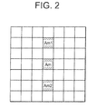
- the second determination unit 5b firstly extracts a pair of pixels Am1 and Am2 that are located above and below the defective pixel candidate Am and that have approximately the same color as the defective pixel candidate Am, and calculates the mean value ((Dm1 + Dm2) /2) of pixel data Dm1 and Dm2 of the extracted pixels Am1 and Am2. Then, when the difference ⁇ between the calculated mean value and the pixel data Dm of the defective pixel candidate Am is the third threshold value Th3 or greater ((Dm1 + Dm2)/2 - Dm ⁇ Th3), the second determination unit 5b determines that the defective pixel Ak is a white defect (see FIG. 2 ) .
- the second determination unit 5b firstly extracts the pair of pixels Am1 and Am2 that are located above and below the defective pixel candidate Am and that have approximately the same color as the defective pixel candidate Am. Then, the second determination unit 5b calculates the mean value of the pixel data Dm1 and Dm2 of the extracted pixels Am1 and Am2. Thereafter, when the difference ⁇ between the calculated mean value and the pixel data Dm of the defective pixel candidate Am is the fourth threshold value Th4 or less ((Dm1 + Dm2) /2 - Dm ⁇ Th4), the second determination unit 5b determines that the defective pixel Ak is a black defect. The second determination unit 5b outputs the determined defective pixel Ak to the defective pixel correction unit 5c. Note that a determination method employed by the second determination unit 5b is not limited to the example described above, and a known determination method may be employed as long as a highly accurate determination is possible.
- the second determination unit 5b firstly extracts the pair of pixels Am1 and Am2 that are located above and below the defective pixel candidate Am and that have approximately the same color as the defective pixel candidate Am. Then, the second determination unit 5b calculates the mean value of the pixel data Dm1 and Dm2 of the extracted pixels Am1 and Am2. However, instead of this, a mean value of pixel data Dn of the pixels An located to the left and right of or diagonally above and below the defective pixel candidate Am may be calculated. Further, the second determination unit 5b may firstly estimate a normal pixel based on a background pattern of an image, and then calculate a mean value of pixel data of the pixels around the defective pixel candidate Am among the estimated normal pixels.
- the defective pixel correction unit 5c performs correction of pixel data Dk of the defective pixel Ak determined by the second determination unit 5b (defective pixel correction step P3). For example, the defective pixel correction unit 5c substitutes the pixel data Dk of the defective pixel Ak with a mean value ((Dk1 + Dk2)/2 of pixel data Dk1 and Dk2 of a pair of pixels Ak1 and Ak2 that are located above and below the defective pixel Ak outputted from the second determination unit 5b and that have approximately the same color as the defective pixel Ak.
- a correction method of the defective pixel taken by the defective pixel correction unit 5c is not limited to the example described above, and a known correction method that enables high processing speed and processing accuracy may be employed.
- the defective pixel correction unit 5c corrects the pixel data Dk of all of the defective pixels Ak, and outputs the pixel data Dk to the memory unit 6 and the output unit 7.
- the defective pixel processing device 5 includes a central processing unit (CPU) that performs arithmetic processing or the like, a read only memory (ROM) that stores an arithmetic program or the like executed by the CPU, and a random access memory (RAM) that temporarily stores processing data or the like.
- the first determination unit 5a, the second determination unit 5b, and the defective pixel correction unit 5c are, for example, stored in the ROM and realized by the program executed by the CPU.
- the defective pixel processing device 5 includes a known image processing function other than the functions described above.
- the defective pixel processing device 5 performs image processing compliant with a picture signal specification such as color separation, white balance, and gamma correction as well as D/A conversion processing on the pixel data Dn outputted from all of the pixels An of the imaging device 3 via the A/D conversion unit 4. Then, the defective pixel processing device 5 converts the resultant pixel data Dn to a video signal of an appropriate format, and outputs the video signal to the output unit 7.
- the memory unit 6 sequentially stores the pixel data Dn of all of the pixels An including the pixel data Dk of the defective pixel Ak corrected by the defective pixel correction unit 5c.
- the memory unit 6 is configured of, for example, a nonvolatile memory, i.e., an EEPROM, a backup RAM, or the like.
- the output unit 7 outputs, as a taken image, the pixel data Dn of all of the pixels An including the pixel data Dk of the defective pixel Ak corrected by the defective pixel correction unit 5c.
- the output unit 7 is configured of an arbitrary display device, e.g., a liquid crystal display device, an organic EL display device, or the like.
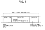
- FIG. 3 is a view schematically showing a processing content for one pixel of the imaging device 3 described above.
- the processing for one pixel An includes the first determination step P1, the second determination step P2, and/or the defective pixel correction step P3.
- the determination processing can be performed speedily as compared with the second determination step P2.
- the second determination step P2 is the comparison between the pixel data Dm of the defective pixel candidate Am and the pixel data Dmn of the pixels Amn around the defective pixel candidate Am as described above, the determination processing can be performed accurately as compared with the first determination step P1. In this manner, the defective pixel candidates Am are first narrowed down speedily by the first determination step P1 of high speed, and then the final defective pixel Ak is accurately determined from the narrowed down defective pixel candidates Am by the second determination step P2.
- a conventional defective pixel processing device may take a lot of time to perform the processing since a comparison needs to be performed between pixel data outputted from all pixels of an imaging device and pixel data of pixels therearound, for example. Instead, if the processing is performed only by simply comparing the pixel data of each pixel of the imaging device with a threshold value, high-speed processing is possible. In this case, however, another problem arises that a normal pixel may be erroneously detected as a defective pixel when the threshold value is set strict, whereas, a defective pixel may fail to be detected when the threshold value is set loose. Thus, the detection accuracy may decrease.
- the defective pixel processing device 5 includes: the first determination unit 5a that compares the pixel data Dn of each pixel An outputted from the imaging device 3 with the first and second threshold values Th1 and Th2 so as to determine whether or not each pixel An is the defective pixel candidate Am; and the second determination unit 5b that compares the pixel data Dm of the defective pixel candidate Am determined by the first determination unit 5a with the pixel data Dmn of the pixels Amn around the defective pixel candidate Am so as to determine whether or not the defective pixel candidate Am is the defective pixel Ak.
- the first determination unit 5a which simply compares the pixel data Dn of each pixel An with the first and second threshold values Th1 and Th2 and thus is capable of performing the determination processing speedily, narrows down the defective pixel candidates Am from all of the pixels An.
- the first determination step P1 the pixels of a large part of all of the pixels An are excluded, as normal pixels, from objects of both the subsequent second determination step P2 and defective pixel correction step P3 that require processing time, as shown in FIG. 4 , for example.
- the overall processing time can be shortened considerably, and the processing speed can be increased.
- the second determination unit 5b which performs the comparison between the pixel data Dm of the defective pixel candidate Am and the pixel data Dmn of the pixels Amn around the defective pixel candidate Am and thus is capable of performing the determination processing accurately, determines the final defective pixel Ak with high accuracy from the narrowed down defective pixel candidates Am.
- the first determination unit 5a which is capable of performing the determination processing speedily, effectively narrows down the defective pixel candidates Am from all of the pixels An, and moreover, the second determination unit 5b, which is capable of performing the determination processing accurately, determines the final defective pixel Ak accurately from the narrowed down defective pixel candidates Am.
- the determination processing of the defective pixel Ak can be performed accurately while the determination processing of the defective pixel candidates Am can be performed speedily. In other words, the defective pixel Ak can be determined speedily and accurately.
- FIGS. 5 and 6 are flowcharts each showing one example of the processing flow of the defective pixel processing device 5 according to one embodiment of the present invention.
- the defective pixel processing device 5 performs one-pixel processing on the pixel data Dn outputted from each pixel An of the imaging device 3 (step S100).
- the one-pixel processing includes the first determination step P1, the second determination step P2, and/or the defective pixel correction step P3. Then, upon judging that the one-pixel processing is finished for the pixel data Dn of all of the pixels An (YES in step S110), the defective pixel processing device 5 ends this defective pixel processing.
- the imaging device 3 outputs the pixel data Dn of each pixel An to the first determination unit 5a via the A/D conversion unit 4 (step S101).
- the first determination unit 5a determines whether or not the pixel data Dn of each pixel An of the imaging device 3 outputted from the A/D conversion unit 4 is within an acceptable value range (Th2 ⁇ Dn ⁇ Th1) that is less than the first threshold value Th1 and greater than the second threshold value Th2 (step S102).
- the first determination unit 5a determines that the pixel An is the defective pixel candidate Am, and proceeds to the next second determination step P2. Accordingly, the defective pixel candidates Am can be narrowed down speedily from all of the pixels An.
- the first determination unit 5a ends the one-pixel processing. Accordingly, a normal pixel within the acceptable value range is excluded from objects of the subsequent second determination step P2 and defective pixel correction step P3 that require processing time. Thus, the overall processing time can be reduced considerably, and the processing speed can be increased.
- the second determination unit 5b determines whether or not the calculated difference ⁇ is within an acceptable value range (Th4 ⁇ ⁇ ⁇ Th3) that is less than the third threshold value Th3 and greater than the fourth threshold value Th4 (step S105).
- the second determination unit 5b determines that the defective pixel candidate Am is the defective pixel Ak, and proceeds to the next defective pixel correction step P3. Accordingly, the final defective pixel. Ak is determined accurately from the defective pixel candidates Am narrowed down by the first determination unit 5a.
- the second determination unit 5b ends the one-pixel processing.
- the defective pixel correction unit 5c substitutes the pixel data Dk of the defective pixel Ak with the mean value ((Dk1 + Dk2)/2) of the pixel data Dk1 and Dk2 of the pair of pixels Ak1 and Ak2 that are located above and below the defective pixel Ak outputted from the second determination unit 5b and that have approximately the same color as the defective pixel Ak (step S106). Then, the defective pixel correction unit 5c ends the one-pixel processing.
- the defective pixel processing device 5 includes the first determination unit 5a that compares the pixel data Dn of each pixel An outputted from the imaging device 3 with the first and second threshold values Th1 and Th2 so as to determine whether or not each pixel An is the defective pixel candidate Am and the second determination unit 5b that compares the pixel data Dm of the defective pixel candidate Am determined by the first determination unit 5a with the pixel data Dmn of the pixels Amn around the defective pixel candidate Am so as to determine whether or not the defective pixel candidate Am is the defective pixel Ak. Accordingly, the defective pixel Ak can be determined speedily and accurately.
- the defective pixel processing device 5 can not only correct a white defect and a black defect of the imaging device 3 at the time of factory shipment of the camera apparatus 1 but also correct in real time a white defect and a black defect of the imaging device 3 caused during imaging or after imaging by the camera apparatus 1.
- the defective pixel processing device 5 is highly user-friendly. Further, since the defective pixel Ak can be determined speedily and accurately as described above with a simple configuration, the use of the device leads to a cost reduction.
Landscapes
- Engineering & Computer Science (AREA)
- Multimedia (AREA)
- Signal Processing (AREA)
- Physics & Mathematics (AREA)
- General Physics & Mathematics (AREA)
- Theoretical Computer Science (AREA)
- Transforming Light Signals Into Electric Signals (AREA)
Abstract
Description
- The present invention relates to a defective pixel processing device and a defective pixel processing method, and more specifically relates to a defective pixel processing device and a defective pixel processing method in which: on the basis of pixel data of each pixel outputted from an imaging device, whether or not each pixel is a defective pixel candidate is determined, and whether or not the determined defective pixel candidate is a defective pixel is further determined.
- Conventionally, a defective pixel detecting method has been known in which: pieces of pixel data outputted from neighboring pixels located around a predetermined pixel are extracted; a maximum value, a mean value, and a minimum value of the pieces of pixel data are calculated; then a comparison is performed to find out which of these values the value of each piece of the pixel data is closest to; and whether or not the predetermined pixel is a defective pixel is determined (for example, see Japanese Patent Application Publication No.
2006-229626 - However, the conventional pixel data detecting method requires much processing time since the foregoing comparison processing needs to be performed on the neighboring pixels of all of the predetermined pixels. Instead of this detection method, another method may be employed in which a defective pixel is determined by simply comparing all of the predetermined pixels with a threshold value. In this case, however, another problem arises that a normal pixel may be erroneously detected as a defective pixel when the threshold value is set strict, whereas, a defective pixel can fail to be detected when the threshold value is set loose. Thus, the detection accuracy may decrease.
- One aspect of the present Invention provides a defective pixel processing device including: first determination means that compares pixel data of each of pixels outputted from an imaging device with a threshold value so as to determine whether or not each of the pixels is a defective pixel candidate; and second determination means that compares the pixel data of the defective pixel candidate determined by the first determination means with the pixel data of the pixels around the defective pixel candidate so as to determine whether or not the defective pixel candidate is a defective pixel. According to this one aspect, the first determination means, which is capable of performing determination processing speedily, determines the defective pixel candidate, and then the second determination means, which is capable of performing determination processing accurately, determines the defective pixel from the narrowed down defective pixel candidates. Accordingly, the defective pixel can be determined speedily and accurately.
- Another aspect of the present invention may be a defective pixel processing method including: a first determination step of comparing pixel data of each of pixels outputted from an imaging device with a threshold value so as to determine whether or not each of the pixels is a defective pixel candidate; and a second determination step of comparing the pixel data of the defective pixel candidate determined in the first determination step with the pixel data of the pixels around the defective pixel candidate so as to determine whether or not the defective pixel candidate is a defective pixel.
- According to the present invention, the defective pixel can be determined speedily and accurately.
-
-
FIG. 1 is a block diagram schematically showing a system configuration of a camera apparatus embedded with a defective pixel processing device according to one embodiment of the present invention. -
FIG. 2 is a view showing positions of pixels of the same color above and below a defective pixel candidate. -
FIG. 3 is a view schematically showing a processing content for one pixel of an imaging device. -
FIG. 4 is a view showing one example of a processing content for all pixels of the imaging device. -
FIG. 5 is a flowchart showing one example of a processing flow of the defective pixel processing device according to one embodiment of the present invention. -
FIG. 6 is a flowchart showing one example of a processing flow of the defective pixel processing device according to one embodiment of the present invention. - Hereinafter, one embodiment will be described as a preferred embodiment for carrying out the present invention with reference to the accompanying drawings.
FIG. 1 is a block diagram schematically showing a system configuration of a camera apparatus embedded with a defective pixel processing device according to one embodiment of the present invention. - A camera apparatus 1 according to this embodiment includes an imaging opticalsystem2, an
imaging device 3, an A/D conversion unit 4, a defectivepixel processing device 5, amemory unit 6, and anoutput unit 7, and is capable of imaging a subject such as a material object. - The imaging
optical system 2 mainly includes a lensoptical system 2a configured of lenses and a light-blocking mechanism 2b, such as an aperture or a shutter, arranged in front of the lensoptical system 2a to block light from a subject. - As the
imaging device 3, a charge coupled device (CCD) or a complementary metal oxide semiconductor (CMOS) device is used, for example. Theimaging device 3 is configured of pixels A1 to An. Incident light from a subject which has passed through the light-blocking mechanism 2b and the lensoptical system 2a of the imagingoptical system 2 forms an image on pixels An of theimaging device 3. Each pixel An of theimaging device 3 performs photoelectric conversion on the incident light and outputs pixel data (for example, brightness value) Dn to the A/D conversion unit 4. - The A/
D conversion unit 4 converts the analog pixel data Dn outputted from each pixel An of theimaging device 3 to digital pixel data Dn, and outputs the digital pixel data Dn to the defectivepixel processing device 5. - The defective
pixel processing device 5 includes afirst determination unit 5a, asecond determination unit 5b, and a defectivepixel correction unit 5c. - The
first determination unit 5a compares the pixels data Dn of all pixels An of theimaging device 3 outputted from the A/D conversion unit 4 with a threshold value Th, and then determines whether or not each pixel An is a defective pixel candidate Am (first determination step P1). - For example, when the pixel date Dn of each pixel An of the
imaging device 3 outputted from the A/D conversion unit 4 is a first threshold value Th1 or greater (Dn ≥ Th1), thefirst determination unit 5a determines that the defective pixel candidate Am may be a white defect. When the pixel data Dn of each pixel An of theimaging device 3 outputted from the A/D conversion unit 4 is a second threshold value Th2 or less (Dn ≤ Th2), thefirst determination unit 5a determines that the defective pixel candidate Am may be a black defect. Note that a determination method employed by thefirst determination unit 5a is not limited to the example described above, and a known determination method may be employed. - As the first threshold value Th1, a value at which the pixel data may be a white defect is obtained by experiment in advance and is stored in the
memory unit 6. In a similar manner, as the second threshold value Th2, a value at which the pixel data may be a black defect is obtained by experiment in advance and is stored in thememory unit 6. - Here, the white defect refers to a defective pixel that appears as a white dot of high brightness when a bypass voltage that is always constant is added to an imaging output in accordance with an incident light for example. On the other hand, the black defect refers to a defective pixel that appears as a black dot of low brightness due to low photoelectric sensitivity, for example. The
first determination unit 5a outputs the determined defective pixel candidate Am to thesecond determination unit 5b. - The
second determination unit 5b compares pixel data Dm of the defective pixel candidates Am outputted from thefirst determination unit 5a with pixel data Dmn of pixels Amn around the defective pixel candidates Am, and then determines whether or not the defective pixel candidate Am is a defective pixel Ak (second determination step P2). - For example, when a difference δ between a mean value of the pixel data Dmn of the pixels Amn around the defective pixel candidate Am and the pixel data Dm of the defective pixel candidate Am is a third threshold value Th3 or greater, the
second determination unit 5b determines that the defective pixel Ak is a white defect. On the other hand, when the difference δ between the mean value of the pixel data Dmn of the pixels Amn around the defective pixel candidate Am and the pixel data Dm of the defective pixel candidate Am is a fourth threshold value Th4 or less, thesecond determination unit 5b determines that the defective pixel Ak is a black defect. - More specifically, the
second determination unit 5b firstly extracts a pair of pixels Am1 and Am2 that are located above and below the defective pixel candidate Am and that have approximately the same color as the defective pixel candidate Am, and calculates the mean value ((Dm1 + Dm2) /2) of pixel data Dm1 and Dm2 of the extracted pixels Am1 and Am2. Then, when the difference δ between the calculated mean value and the pixel data Dm of the defective pixel candidate Am is the third threshold value Th3 or greater ((Dm1 + Dm2)/2 - Dm ≥ Th3), thesecond determination unit 5b determines that the defective pixel Ak is a white defect (seeFIG. 2 ) . - In a similar manner, the
second determination unit 5b firstly extracts the pair of pixels Am1 and Am2 that are located above and below the defective pixel candidate Am and that have approximately the same color as the defective pixel candidate Am. Then, thesecond determination unit 5b calculates the mean value of the pixel data Dm1 and Dm2 of the extracted pixels Am1 and Am2. Thereafter, when the difference δ between the calculated mean value and the pixel data Dm of the defective pixel candidate Am is the fourth threshold value Th4 or less ((Dm1 + Dm2) /2 - Dm ≤ Th4), thesecond determination unit 5b determines that the defective pixel Ak is a black defect. Thesecond determination unit 5b outputs the determined defective pixel Ak to the defectivepixel correction unit 5c. Note that a determination method employed by thesecond determination unit 5b is not limited to the example described above, and a known determination method may be employed as long as a highly accurate determination is possible. - For example, the
second determination unit 5b firstly extracts the pair of pixels Am1 and Am2 that are located above and below the defective pixel candidate Am and that have approximately the same color as the defective pixel candidate Am. Then, thesecond determination unit 5b calculates the mean value of the pixel data Dm1 and Dm2 of the extracted pixels Am1 and Am2. However, instead of this, a mean value of pixel data Dn of the pixels An located to the left and right of or diagonally above and below the defective pixel candidate Am may be calculated. Further, thesecond determination unit 5b may firstly estimate a normal pixel based on a background pattern of an image, and then calculate a mean value of pixel data of the pixels around the defective pixel candidate Am among the estimated normal pixels. - The defective
pixel correction unit 5c performs correction of pixel data Dk of the defective pixel Ak determined by thesecond determination unit 5b (defective pixel correction step P3). For example, the defectivepixel correction unit 5c substitutes the pixel data Dk of the defective pixel Ak with a mean value ((Dk1 + Dk2)/2 of pixel data Dk1 and Dk2 of a pair of pixels Ak1 and Ak2 that are located above and below the defective pixel Ak outputted from thesecond determination unit 5b and that have approximately the same color as the defective pixel Ak. - Note that a correction method of the defective pixel taken by the defective
pixel correction unit 5c is not limited to the example described above, and a known correction method that enables high processing speed and processing accuracy may be employed. As described above, the defectivepixel correction unit 5c corrects the pixel data Dk of all of the defective pixels Ak, and outputs the pixel data Dk to thememory unit 6 and theoutput unit 7. - As a main hardware configuration, the defective
pixel processing device 5 includes a central processing unit (CPU) that performs arithmetic processing or the like, a read only memory (ROM) that stores an arithmetic program or the like executed by the CPU, and a random access memory (RAM) that temporarily stores processing data or the like. Thefirst determination unit 5a, thesecond determination unit 5b, and the defectivepixel correction unit 5c are, for example, stored in the ROM and realized by the program executed by the CPU. - Further, the defective
pixel processing device 5 includes a known image processing function other than the functions described above. For example, the defectivepixel processing device 5 performs image processing compliant with a picture signal specification such as color separation, white balance, and gamma correction as well as D/A conversion processing on the pixel data Dn outputted from all of the pixels An of theimaging device 3 via the A/D conversion unit 4. Then, the defectivepixel processing device 5 converts the resultant pixel data Dn to a video signal of an appropriate format, and outputs the video signal to theoutput unit 7. - The
memory unit 6 sequentially stores the pixel data Dn of all of the pixels An including the pixel data Dk of the defective pixel Ak corrected by the defectivepixel correction unit 5c. Thememory unit 6 is configured of, for example, a nonvolatile memory, i.e., an EEPROM, a backup RAM, or the like. - The
output unit 7 outputs, as a taken image, the pixel data Dn of all of the pixels An including the pixel data Dk of the defective pixel Ak corrected by the defectivepixel correction unit 5c. Theoutput unit 7 is configured of an arbitrary display device, e.g., a liquid crystal display device, an organic EL display device, or the like. -
FIG. 3 is a view schematically showing a processing content for one pixel of theimaging device 3 described above. As shown inFIG. 3 , the processing for one pixel An includes the first determination step P1, the second determination step P2, and/or the defective pixel correction step P3. - Additionally, since the first determination step P1 is the comparison between the pixel data Dn of each pixel An and the first and second threshold values and Th2 as described above, the determination processing can be performed speedily as compared with the second determination step P2. On the other hand, since the second determination step P2 is the comparison between the pixel data Dm of the defective pixel candidate Am and the pixel data Dmn of the pixels Amn around the defective pixel candidate Am as described above, the determination processing can be performed accurately as compared with the first determination step P1. In this manner, the defective pixel candidates Am are first narrowed down speedily by the first determination step P1 of high speed, and then the final defective pixel Ak is accurately determined from the narrowed down defective pixel candidates Am by the second determination step P2.
- In contrast, a conventional defective pixel processing device may take a lot of time to perform the processing since a comparison needs to be performed between pixel data outputted from all pixels of an imaging device and pixel data of pixels therearound, for example. Instead, if the processing is performed only by simply comparing the pixel data of each pixel of the imaging device with a threshold value, high-speed processing is possible. In this case, however, another problem arises that a normal pixel may be erroneously detected as a defective pixel when the threshold value is set strict, whereas, a defective pixel may fail to be detected when the threshold value is set loose. Thus, the detection accuracy may decrease.
- To deal with this problem, the defective
pixel processing device 5 according to this embodiment includes: thefirst determination unit 5a that compares the pixel data Dn of each pixel An outputted from theimaging device 3 with the first and second threshold values Th1 and Th2 so as to determine whether or not each pixel An is the defective pixel candidate Am; and thesecond determination unit 5b that compares the pixel data Dm of the defective pixel candidate Am determined by thefirst determination unit 5a with the pixel data Dmn of the pixels Amn around the defective pixel candidate Am so as to determine whether or not the defective pixel candidate Am is the defective pixel Ak. - Accordingly, the
first determination unit 5a, which simply compares the pixel data Dn of each pixel An with the first and second threshold values Th1 and Th2 and thus is capable of performing the determination processing speedily, narrows down the defective pixel candidates Am from all of the pixels An. By this first determination step P1, the pixels of a large part of all of the pixels An are excluded, as normal pixels, from objects of both the subsequent second determination step P2 and defective pixel correction step P3 that require processing time, as shown inFIG. 4 , for example. Thus, the overall processing time can be shortened considerably, and the processing speed can be increased. Further, thesecond determination unit 5b, which performs the comparison between the pixel data Dm of the defective pixel candidate Am and the pixel data Dmn of the pixels Amn around the defective pixel candidate Am and thus is capable of performing the determination processing accurately, determines the final defective pixel Ak with high accuracy from the narrowed down defective pixel candidates Am. - In this manner, the
first determination unit 5a, which is capable of performing the determination processing speedily, effectively narrows down the defective pixel candidates Am from all of the pixels An, and moreover, thesecond determination unit 5b, which is capable of performing the determination processing accurately, determines the final defective pixel Ak accurately from the narrowed down defective pixel candidates Am. Thus, the determination processing of the defective pixel Ak can be performed accurately while the determination processing of the defective pixel candidates Am can be performed speedily. In other words, the defective pixel Ak can be determined speedily and accurately. - Next, a processing flow of the defective
pixel processing device 5 according to this embodiment described above will be described in detail.FIGS. 5 and6 are flowcharts each showing one example of the processing flow of the defectivepixel processing device 5 according to one embodiment of the present invention. - As shown in
FIG. 5 , the defectivepixel processing device 5 performs one-pixel processing on the pixel data Dn outputted from each pixel An of the imaging device 3 (step S100). Here the one-pixel processing includes the first determination step P1, the second determination step P2, and/or the defective pixel correction step P3. Then, upon judging that the one-pixel processing is finished for the pixel data Dn of all of the pixels An (YES in step S110), the defectivepixel processing device 5 ends this defective pixel processing. - Next, the one-pixel processing of the defective
pixel processing device 5 described above will be described in detail. As shown inFIG. 6 , theimaging device 3 outputs the pixel data Dn of each pixel An to thefirst determination unit 5a via the A/D conversion unit 4 (step S101). - In the first determination step P1, the
first determination unit 5a determines whether or not the pixel data Dn of each pixel An of theimaging device 3 outputted from the A/D conversion unit 4 is within an acceptable value range (Th2 < Dn < Th1) that is less than the first threshold value Th1 and greater than the second threshold value Th2 (step S102). - Upon determining that the pixel data Dn of each pixel An of the
imaging device 3 is not within the acceptable value range (Dn ≤ Th2 or Dn ≤ Th1) (NO in step S102), thefirst determination unit 5a determines that the pixel An is the defective pixel candidate Am, and proceeds to the next second determination step P2. Accordingly, the defective pixel candidates Am can be narrowed down speedily from all of the pixels An. - On the other hand, upon determining that the pixel data Dn of each pixel An of the
imaging device 3 is within the acceptable value range (YES in step 102), thefirst determination unit 5a ends the one-pixel processing. Accordingly, a normal pixel within the acceptable value range is excluded from objects of the subsequent second determination step P2 and defective pixel correction step P3 that require processing time. Thus, the overall processing time can be reduced considerably, and the processing speed can be increased. - In the second determination step P2, the
second determination unit 5b extracts the pair of pixels Am1 and Am2 that are located above and below the defective pixel candidate Am and that have approximately the same color as the defective pixel candidate Am. Then, thesecond determination unit 5b calculates the mean value ((Dm1 + Dm2) /2) of the pixel data Dm1 and Dm2 of the extracted pixels Am1 and Am2 (step S103). Also, thesecond determination unit 5b calculates the difference δ (δ = (Dm1 + Dm2)/2 - Dm) between the calculated mean value and the pixel data Dm of the defective pixel candidate Am (step S104). - The
second determination unit 5b determines whether or not the calculated difference δ is within an acceptable value range (Th4 < δ < Th3) that is less than the third threshold value Th3 and greater than the fourth threshold value Th4 (step S105). - Upon determining that the calculated difference δ is not within the acceptable value range (Dn ≤ Th4 or Dn ≥ Th3) (NO in step S105), the
second determination unit 5b determines that the defective pixel candidate Am is the defective pixel Ak, and proceeds to the next defective pixel correction step P3. Accordingly, the final defective pixel. Ak is determined accurately from the defective pixel candidates Am narrowed down by thefirst determination unit 5a. - On the other hand, upon determining that the calculated difference δ is within the acceptable value range (YES in step S105), the
second determination unit 5b ends the one-pixel processing. - In the defective pixel correction step P3, the defective
pixel correction unit 5c substitutes the pixel data Dk of the defective pixel Ak with the mean value ((Dk1 + Dk2)/2) of the pixel data Dk1 and Dk2 of the pair of pixels Ak1 and Ak2 that are located above and below the defective pixel Ak outputted from thesecond determination unit 5b and that have approximately the same color as the defective pixel Ak (step S106). Then, the defectivepixel correction unit 5c ends the one-pixel processing. - As described above, the defective
pixel processing device 5 according to this embodiment includes thefirst determination unit 5a that compares the pixel data Dn of each pixel An outputted from theimaging device 3 with the first and second threshold values Th1 and Th2 so as to determine whether or not each pixel An is the defective pixel candidate Am and thesecond determination unit 5b that compares the pixel data Dm of the defective pixel candidate Am determined by thefirst determination unit 5a with the pixel data Dmn of the pixels Amn around the defective pixel candidate Am so as to determine whether or not the defective pixel candidate Am is the defective pixel Ak. Accordingly, the defective pixel Ak can be determined speedily and accurately. - The defective
pixel processing device 5 according to this embodiment can not only correct a white defect and a black defect of theimaging device 3 at the time of factory shipment of the camera apparatus 1 but also correct in real time a white defect and a black defect of theimaging device 3 caused during imaging or after imaging by the camera apparatus 1. Thus, the defectivepixel processing device 5 is highly user-friendly. Further, since the defective pixel Ak can be determined speedily and accurately as described above with a simple configuration, the use of the device leads to a cost reduction. - Although the inventions has been described above in connection with several preferred embodiments thereof, it will be appreciated by those skilled in the art that those embodiments are provided solely for illustrating the invention, and should not be relied upon to construe the appended claims in a limiting sense.
Claims (7)
- A defective pixel processing device comprising:first determination means that determines whether or not each of pixels outputted from an imaging device is a defective pixel candidate by comparing pixel data of said each of pixels with a threshold value; andsecond determination means that determines whether or not said defective pixel candidate determined by said first determination means is a defective pixel by comparing pixel data of said defective pixel candidate with pixel data of some pixels around said defective pixel candidate.
- The defective pixel processing device according to claim 1, wherein said first determination means determines that said defective pixel candidate may be a white defect when said pixel data takes a first threshold value or greater, and determines that said defective pixel candidate may be a black defect when said pixel data takes a second threshold value or less.
- The defective pixel processing device according to claim 2, wherein said second determination means determines that said defective pixel is a white defect when a difference between a mean value of pixel data of said some pixels around said defective pixel candidate and pixel data of said defective pixel candidate has a third threshold value or greater, and determines that said defective pixel is a black defect when said difference between said mean value of pixel data of said some pixels around said defective pixel candidate and pixel data of said defective pixel candidate has a fourth threshold value or less.
- The defective pixel processing device according to claim 3, wherein said second determination means extracts two pixels that are located above and below said defective pixel candidate and that have a color approximately identical to said defective pixel candidate, and calculates a mean value of pixel data of said extracted pixels.
- The defective pixel processing device according to any of claims 1 to 4, further comprising defective pixel correction means that corrects pixel data of said defective pixel determined by said second determination means.
- The defective pixel processing device according to claim 5, wherein said defective pixel correction means substitutes pixel data of said defective pixel with a mean value of pixel data of said some pixels around said defective pixel.
- A defective pixel processing method comprising:a first determination step of determining whether or not each of pixels outputted from an imaging device is a defective pixel candidate by comparing pixel data of said each pixels with a threshold value; anda second determination step of determining whether or not said defective pixel candidate determined in said first determination step is a defective pixel by comparing pixel data of said defective pixel candidate with pixel data of some pixels around said defective pixel candidate.
Applications Claiming Priority (1)
| Application Number | Priority Date | Filing Date | Title |
|---|---|---|---|
| JP2008152808A JP2009302722A (en) | 2008-06-11 | 2008-06-11 | Defective pixel processing device and defective pixel processing method |
Publications (2)
| Publication Number | Publication Date |
|---|---|
| EP2134076A2 true EP2134076A2 (en) | 2009-12-16 |
| EP2134076A3 EP2134076A3 (en) | 2012-11-21 |
Family
ID=40875148
Family Applications (1)
| Application Number | Title | Priority Date | Filing Date |
|---|---|---|---|
| EP09162332A Withdrawn EP2134076A3 (en) | 2008-06-11 | 2009-06-09 | Defective pixel processing device and defective pixel processing method |
Country Status (5)
| Country | Link |
|---|---|
| US (1) | US20090310849A1 (en) |
| EP (1) | EP2134076A3 (en) |
| JP (1) | JP2009302722A (en) |
| KR (1) | KR101056978B1 (en) |
| TW (1) | TW201011280A (en) |
Families Citing this family (10)
| Publication number | Priority date | Publication date | Assignee | Title |
|---|---|---|---|---|
| US9294690B1 (en) * | 2008-04-10 | 2016-03-22 | Cyan Systems, Inc. | System and method for using filtering and pixel correlation to increase sensitivity in image sensors |
| JP2013038504A (en) * | 2011-08-04 | 2013-02-21 | Sony Corp | Imaging device, image processing method and program |
| JP2013050538A (en) | 2011-08-30 | 2013-03-14 | Sony Corp | Display device and electronic apparatus |
| JP2013168793A (en) * | 2012-02-15 | 2013-08-29 | Toshiba Corp | Image processing device |
| JP5968025B2 (en) * | 2012-04-11 | 2016-08-10 | キヤノン株式会社 | IMAGING DEVICE AND IMAGING DEVICE CONTROL METHOD |
| JP6071333B2 (en) | 2012-08-27 | 2017-02-01 | キヤノン株式会社 | Image processing apparatus, method and program, and imaging apparatus having image processing apparatus |
| JP6291940B2 (en) * | 2014-03-20 | 2018-03-14 | 株式会社ソシオネクスト | Defective pixel correction device, imaging device, and defective pixel correction method |
| DE102018122048A1 (en) * | 2017-09-11 | 2019-03-14 | Vuereal Inc. | REPAIR TECHNOLOGIES FOR MICRO-LED DEVICES AND ARRAYS |
| JP6503524B1 (en) * | 2017-10-05 | 2019-04-17 | オリンパス株式会社 | Processing device, endoscope, endoscope system, image processing method and program |
| KR20240114118A (en) * | 2023-01-16 | 2024-07-23 | 에스케이하이닉스 주식회사 | Image processing device and image processing method |
Citations (1)
| Publication number | Priority date | Publication date | Assignee | Title |
|---|---|---|---|---|
| JP2006229626A (en) | 2005-02-17 | 2006-08-31 | Fuji Photo Film Co Ltd | Defective pixel detecting method |
Family Cites Families (14)
| Publication number | Priority date | Publication date | Assignee | Title |
|---|---|---|---|---|
| US5537669A (en) * | 1993-09-30 | 1996-07-16 | Kla Instruments Corporation | Inspection method and apparatus for the inspection of either random or repeating patterns |
| JP3785520B2 (en) * | 1997-03-19 | 2006-06-14 | コニカミノルタホールディングス株式会社 | Electronic camera |
| JP2006174497A (en) * | 1999-10-27 | 2006-06-29 | Sanyo Electric Co Ltd | Image signal processing device |
| JP3773773B2 (en) * | 1999-10-27 | 2006-05-10 | 三洋電機株式会社 | Image signal processing apparatus and pixel defect detection method |
| JP2002281391A (en) * | 2001-03-16 | 2002-09-27 | Olympus Optical Co Ltd | Imaging system |
| JP3912672B2 (en) * | 2002-07-05 | 2007-05-09 | ソニー株式会社 | Solid-state imaging device and pixel defect inspection method thereof |
| JP4194336B2 (en) * | 2002-07-25 | 2008-12-10 | 富士通マイクロエレクトロニクス株式会社 | Semiconductor integrated circuit, defective pixel correction method, and image processor |
| JP4288954B2 (en) | 2003-02-06 | 2009-07-01 | ソニー株式会社 | Defect detection circuit and defect detection method |
| JP2006026234A (en) * | 2004-07-20 | 2006-02-02 | Olympus Corp | In vivo imaging apparatus and in vivo imaging system |
| JP2006166194A (en) * | 2004-12-09 | 2006-06-22 | Sony Corp | Pixel defect detection circuit and pixel defect detection method |
| JP4745816B2 (en) * | 2005-12-20 | 2011-08-10 | 富士通セミコンダクター株式会社 | Image processing circuit and image processing method |
| JP5043400B2 (en) * | 2006-11-07 | 2012-10-10 | キヤノン株式会社 | Imaging apparatus and control method thereof |
| JP2008131165A (en) * | 2006-11-17 | 2008-06-05 | Rohm Co Ltd | Defective pixel detection device, electronic device, and defective pixel detection program |
| KR100793920B1 (en) * | 2006-11-27 | 2008-01-16 | 삼성전기주식회사 | Real-time bad pixel detection and correction device and method |
-
2008
- 2008-06-11 JP JP2008152808A patent/JP2009302722A/en active Pending
-
2009
- 2009-06-02 US US12/457,152 patent/US20090310849A1/en not_active Abandoned
- 2009-06-04 TW TW098118584A patent/TW201011280A/en unknown
- 2009-06-09 EP EP09162332A patent/EP2134076A3/en not_active Withdrawn
- 2009-06-10 KR KR1020090051376A patent/KR101056978B1/en not_active Expired - Fee Related
Patent Citations (1)
| Publication number | Priority date | Publication date | Assignee | Title |
|---|---|---|---|---|
| JP2006229626A (en) | 2005-02-17 | 2006-08-31 | Fuji Photo Film Co Ltd | Defective pixel detecting method |
Also Published As
| Publication number | Publication date |
|---|---|
| US20090310849A1 (en) | 2009-12-17 |
| KR101056978B1 (en) | 2011-08-16 |
| KR20090129353A (en) | 2009-12-16 |
| JP2009302722A (en) | 2009-12-24 |
| EP2134076A3 (en) | 2012-11-21 |
| TW201011280A (en) | 2010-03-16 |
Similar Documents
| Publication | Publication Date | Title |
|---|---|---|
| US20090310849A1 (en) | Defective pixel processing device and defective pixel processing method | |
| US6625318B1 (en) | Robust sequential approach in detecting defective pixels within an image sensor | |
| US8682068B2 (en) | Image processing apparatus, image processing method, and program | |
| US10348989B2 (en) | Image processing device, image processing method, and image processing system | |
| US20140043506A1 (en) | Method, apparatus and system providing adjustment of pixel defect map | |
| JP7208379B2 (en) | Calibration method | |
| US9438832B2 (en) | Image processing apparatus and image processing method | |
| US10108878B2 (en) | Image processing apparatus, image processing method, and storage medium for tone control of each object region in an image | |
| US9161001B2 (en) | Image capturing apparatus that suppresses color deviation resulting from noise due to temperature and exposure time | |
| US9432601B2 (en) | Defective pixel correcting apparatus, imaging apparatus, and method of correcting defective pixel | |
| CN108029185A (en) | Illuminance acquisition device, lighting control system and program | |
| KR101553707B1 (en) | Image stain detection method for camera module defect determination | |
| CN102572274A (en) | Image signal processing apparatus and image signal processing method | |
| CN108965749A (en) | Defect pixel detection and means for correcting and method based on texture recognition | |
| JP4534825B2 (en) | Defect inspection method and defect inspection apparatus | |
| JP2018007083A (en) | Image processing apparatus | |
| JP6561479B2 (en) | Imaging device capable of color shading correction | |
| JP2009017158A (en) | Camera inspection device | |
| JP6348883B2 (en) | Image capturing apparatus, image capturing method, and computer program | |
| JP4921058B2 (en) | Imaging apparatus and control method thereof | |
| KR102419799B1 (en) | Backlight Determination and Improvement Apparatus and Method between Smartphone Front Ambient Light Sensor and Rear Camera Sensor Using Artificial Object Detection | |
| KR20110044961A (en) | Defective Pixel Processing Devices and Defective Pixel Processing Methods | |
| KR102198748B1 (en) | Method for detecting soft defective pixels in infrared camera for detection of acquired bad pixels | |
| US20060279646A1 (en) | Pixel defect detection method for solid-state image pickup device | |
| JP2006229626A (en) | Defective pixel detecting method |
Legal Events
| Date | Code | Title | Description |
|---|---|---|---|
| PUAI | Public reference made under article 153(3) epc to a published international application that has entered the european phase |
Free format text: ORIGINAL CODE: 0009012 |
|
| AK | Designated contracting states |
Kind code of ref document: A2 Designated state(s): AT BE BG CH CY CZ DE DK EE ES FI FR GB GR HR HU IE IS IT LI LT LU LV MC MK MT NL NO PL PT RO SE SI SK TR |
|
| RAP1 | Party data changed (applicant data changed or rights of an application transferred) |
Owner name: RENESAS ELECTRONICS CORPORATION |
|
| PUAL | Search report despatched |
Free format text: ORIGINAL CODE: 0009013 |
|
| AK | Designated contracting states |
Kind code of ref document: A3 Designated state(s): AT BE BG CH CY CZ DE DK EE ES FI FR GB GR HR HU IE IS IT LI LT LU LV MC MK MT NL NO PL PT RO SE SI SK TR |
|
| RIC1 | Information provided on ipc code assigned before grant |
Ipc: H04N 5/217 20110101AFI20121016BHEP |
|
| STAA | Information on the status of an ep patent application or granted ep patent |
Free format text: STATUS: THE APPLICATION IS DEEMED TO BE WITHDRAWN |
|
| 18D | Application deemed to be withdrawn |
Effective date: 20130522 |